JP4129106B2 - Semiconductor device - Google Patents
Semiconductor device Download PDFInfo
- Publication number
- JP4129106B2 JP4129106B2 JP30530399A JP30530399A JP4129106B2 JP 4129106 B2 JP4129106 B2 JP 4129106B2 JP 30530399 A JP30530399 A JP 30530399A JP 30530399 A JP30530399 A JP 30530399A JP 4129106 B2 JP4129106 B2 JP 4129106B2
- Authority
- JP
- Japan
- Prior art keywords
- layer
- impurity concentration
- semiconductor layer
- semiconductor substrate
- type semiconductor
- Prior art date
- Legal status (The legal status is an assumption and is not a legal conclusion. Google has not performed a legal analysis and makes no representation as to the accuracy of the status listed.)
- Expired - Fee Related
Links
- 239000004065 semiconductor Substances 0.000 title claims description 87
- 239000012535 impurity Substances 0.000 claims description 96
- 239000000758 substrate Substances 0.000 claims description 39
- 230000007423 decrease Effects 0.000 claims description 13
- 229910052751 metal Inorganic materials 0.000 claims description 7
- 239000002184 metal Substances 0.000 claims description 7
- 238000013459 approach Methods 0.000 claims description 2
- 239000007787 solid Substances 0.000 claims description 2
- 230000002441 reversible effect Effects 0.000 description 32
- 238000011084 recovery Methods 0.000 description 17
- 238000009792 diffusion process Methods 0.000 description 15
- 230000010355 oscillation Effects 0.000 description 10
- 238000010438 heat treatment Methods 0.000 description 8
- 239000000969 carrier Substances 0.000 description 6
- 230000005684 electric field Effects 0.000 description 5
- OAICVXFJPJFONN-UHFFFAOYSA-N Phosphorus Chemical compound [P] OAICVXFJPJFONN-UHFFFAOYSA-N 0.000 description 4
- 230000015572 biosynthetic process Effects 0.000 description 4
- 238000000034 method Methods 0.000 description 4
- 229910052698 phosphorus Inorganic materials 0.000 description 4
- 239000011574 phosphorus Substances 0.000 description 4
- 230000006798 recombination Effects 0.000 description 3
- 238000005215 recombination Methods 0.000 description 3
- 229910052710 silicon Inorganic materials 0.000 description 3
- 239000010703 silicon Substances 0.000 description 3
- ZOXJGFHDIHLPTG-UHFFFAOYSA-N Boron Chemical compound [B] ZOXJGFHDIHLPTG-UHFFFAOYSA-N 0.000 description 2
- GYHNNYVSQQEPJS-UHFFFAOYSA-N Gallium Chemical compound [Ga] GYHNNYVSQQEPJS-UHFFFAOYSA-N 0.000 description 2
- 229910052785 arsenic Inorganic materials 0.000 description 2
- RQNWIZPPADIBDY-UHFFFAOYSA-N arsenic atom Chemical compound [As] RQNWIZPPADIBDY-UHFFFAOYSA-N 0.000 description 2
- 229910052796 boron Inorganic materials 0.000 description 2
- 238000007796 conventional method Methods 0.000 description 2
- 230000000694 effects Effects 0.000 description 2
- 238000010894 electron beam technology Methods 0.000 description 2
- 229910052733 gallium Inorganic materials 0.000 description 2
- 229910001385 heavy metal Inorganic materials 0.000 description 2
- 238000005468 ion implantation Methods 0.000 description 2
- 230000007257 malfunction Effects 0.000 description 2
- 238000005259 measurement Methods 0.000 description 2
- 230000002093 peripheral effect Effects 0.000 description 2
- 238000004088 simulation Methods 0.000 description 2
- 230000002123 temporal effect Effects 0.000 description 2
- AAEQXEDPVFIFDK-UHFFFAOYSA-N 3-(4-fluorobenzoyl)-2-(2-methylpropanoyl)-n,3-diphenyloxirane-2-carboxamide Chemical compound C=1C=CC=CC=1NC(=O)C1(C(=O)C(C)C)OC1(C=1C=CC=CC=1)C(=O)C1=CC=C(F)C=C1 AAEQXEDPVFIFDK-UHFFFAOYSA-N 0.000 description 1
- 238000009825 accumulation Methods 0.000 description 1
- 230000002411 adverse Effects 0.000 description 1
- 229910052782 aluminium Inorganic materials 0.000 description 1
- XAGFODPZIPBFFR-UHFFFAOYSA-N aluminium Chemical compound [Al] XAGFODPZIPBFFR-UHFFFAOYSA-N 0.000 description 1
- 238000010586 diagram Methods 0.000 description 1
- 238000004519 manufacturing process Methods 0.000 description 1
- 238000012986 modification Methods 0.000 description 1
- 230000004048 modification Effects 0.000 description 1
- 230000033764 rhythmic process Effects 0.000 description 1
Images


Classifications
-
- H—ELECTRICITY
- H01—ELECTRIC ELEMENTS
- H01L—SEMICONDUCTOR DEVICES NOT COVERED BY CLASS H10
- H01L29/00—Semiconductor devices adapted for rectifying, amplifying, oscillating or switching, or capacitors or resistors with at least one potential-jump barrier or surface barrier, e.g. PN junction depletion layer or carrier concentration layer; Details of semiconductor bodies or of electrodes thereof ; Multistep manufacturing processes therefor
- H01L29/66—Types of semiconductor device ; Multistep manufacturing processes therefor
- H01L29/86—Types of semiconductor device ; Multistep manufacturing processes therefor controllable only by variation of the electric current supplied, or only the electric potential applied, to one or more of the electrodes carrying the current to be rectified, amplified, oscillated or switched
- H01L29/861—Diodes
- H01L29/868—PIN diodes
-
- H—ELECTRICITY
- H01—ELECTRIC ELEMENTS
- H01L—SEMICONDUCTOR DEVICES NOT COVERED BY CLASS H10
- H01L29/00—Semiconductor devices adapted for rectifying, amplifying, oscillating or switching, or capacitors or resistors with at least one potential-jump barrier or surface barrier, e.g. PN junction depletion layer or carrier concentration layer; Details of semiconductor bodies or of electrodes thereof ; Multistep manufacturing processes therefor
- H01L29/02—Semiconductor bodies ; Multistep manufacturing processes therefor
- H01L29/36—Semiconductor bodies ; Multistep manufacturing processes therefor characterised by the concentration or distribution of impurities in the bulk material
Landscapes
- Engineering & Computer Science (AREA)
- Microelectronics & Electronic Packaging (AREA)
- Power Engineering (AREA)
- Physics & Mathematics (AREA)
- Ceramic Engineering (AREA)
- Condensed Matter Physics & Semiconductors (AREA)
- General Physics & Mathematics (AREA)
- Computer Hardware Design (AREA)
- Thyristors (AREA)
- Bipolar Transistors (AREA)
Description
【0001】
【発明の属する技術分野】
本発明は、pin構造を有する半導体装置、例えばダイオード、トランジスタ、サイリスタに関する。
【0002】
【従来の技術】
図15は従来のpinダイオードの構造を示し、同図(a)は断面図、同図(b)は不純物濃度プロファイルである。例えばシリコンを主成分とするn-型半導体基板601は、その一主面側(図中左側)にp層602を、他の主面側(図中右側)にn+層603を、それぞれ備えている。p層602は例えばボロンやガリウムを、n+層603は例えば燐を、それぞれ不純物として採用し、熱処理を行って所定の深さまで拡散して得ることができる。p層602及びn+層603にはそれぞれn-型半導体基板601と反対側に、電気抵抗の小さい金属から成るアノード電極604、カソード電極605が設けられている。
【0003】
n-型半導体基板601の不純物はほぼ均一に分布しており、不純物濃度勾配は非常に小さい。またp層602及び及びn+層603は、その形成がn-型半導体基板601の2つの主面に対する不純物拡散で行われるので、いずれの不純物濃度も、n-型半導体基板601に近づくほど減少する不純物濃度勾配を有している。例えばn+層603の不純物濃度勾配は、約4×1018cm-4である。ここで不純物濃度勾配は、n+層603における不純物濃度の最大値の90%である第1の濃度を有する位置から、最大値の50%である第2の濃度を有する位置までの距離で、第1の濃度と第2の濃度の差を除した値を採用している。
【0004】
一般にpn接合を有するダイオードに対して、外部回路の瞬間的な切替えによって、順方向に電流が流れている状態から逆バイアスを加えようとすると、過渡的にある期間だけ大きな逆電流が流れる。これはダイオードには少数キャリア蓄積現象があって、電流が一旦零になっても、直ちには逆方向に回復しないことによる。この逆電流は接合近傍に過剰キャリアとして残っていた小数キャリアがある濃度以下に減少して、空乏層が確立されるまで続く。
【0005】
空乏層が確立すると、これが逆電圧を支え始め、空乏層の広がりに対応して逆電圧が徐々に増加すると共に逆電流が徐々に減少する。そして素子電圧が逆バイアスに印加された電圧に定常的に等しくなって逆回復動作が完了する。逆回復動作において流れる逆電流は、逆バイアス値と外部回路のインダクタンスで決まる電流減少率で減少する。
【0006】
図15に示されたダイオードでは、p層602とn-型半導体基板601とが形成するpn接合近傍で、プロトン照射等によりキャリア再結合の中心が形成され、pn接合近傍のライフタイムを局部的に短く制御することで順電圧を低く、且つ逆回復電流が小さく、di/dt耐量の高い特性を図っている。またn-型半導体基板601は、全体に重金属の拡散や電子線照射等が施され、キャリアのライフタイムが短くなるように制御されている。
【0007】
【発明が解決しようとする課題】
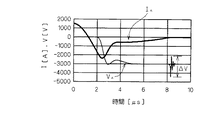
しかしながら逆バイアス電圧が高い場合、逆回復動作の完了時近傍で、ダイオードの印加電圧が急激に振動し、周辺の電気機器の誤動作をもたらすようなノイズを発生させるという問題がある。図16は図15に示されたダイオードの逆回復動作前後の電圧VA、電流IAの時間変化を示すグラフであり、外部回路によって順バイアスから逆バイアスへと切り替えられた時刻を零としている。切り替え後約8μsにおいて、ダイオードの電流が定常的に零となり始め、その直後に2000Vを越える振幅ΔVの電圧振動が生じていることがわかる。
【0008】
このような電圧振動はダイオードと外部回路が形成するLCR直列回路の共振によって生じると考えられる。このLCR直列回路は、ダイオードの空乏層と過剰キャリアをパラメータにした容量成分Cと、ダイオードに対する印加電圧と洩れ電流及び過剰キャリアの再結合電流をパラメータにした抵抗成分Rと、外部回路のインダクタンス成分Lとによって形成される。
【0009】
ダイオードの容量成分Cと抵抗成分Rは時間的に変化する。特に抵抗成分Rは、空乏層外にある過剰キャリアが消滅すると急激に変化する。よってLCR回路の共振条件に達し、図16に示されたように電圧が振動すると考えられる。又、空乏層がn+層603に到達すると容量成分Cが急激に変化し、これがトリガーとなって電圧振動を発生させる場合もある。
【0010】
このような電圧振動はダイオードに限らず、スイッチング速度の速いGCT(gate controlled turn-off)サイリスタなどでも、ターンオフ動作での電圧上昇時に生じうる。かかる電圧振動は、周辺の電気機器の誤動作をもたらすようなノイズの原因になるという問題がある。
【0011】
本発明は上記のような問題を解決するためになされたもので、逆回復動作時やターンオフ動作時に印加電圧に振動の発生が少ない半導体装置を提供することを目的とする。
【0012】
なお、逆回復時の波形を改善する為に半導体層と濃度とを制御する技術が、例えば特開昭62−115880号公報に開示されている。
【0013】
【課題を解決するための手段】
この発明のうち請求項1にかかるものは、第1導電型の第1半導体層と、第2導電型の第2半導体層と、前記第1半導体層と前記第2半導体層の間に介在して前記第2半導体層よりも不純物濃度の低い前記第2導電型の半導体基板とを備える半導体装置であって、前記第2半導体層の不純物濃度は前記半導体基板に近づくにつれて減少し、前記第2半導体層における前記不純物濃度の最大値の90%から50%へと減少する不純物濃度勾配が、1×10 18 cm -4 以上2×1018cm-4以下であり、前記第2半導体層の前記不純物濃度の前記最大値は1×10 15 cm -3 以上5×1015cm-3以下であることを特徴とする。
【0015】
この発明のうち請求項2にかかるものは、請求項1記載の半導体装置であって、前記半導体基板と共に前記第2半導体層を挟む前記第2導電型の第3の半導体層と、前記第2半導体層と共に前記第3半導体層を挟む金属電極とを更に備え、前記第3半導体層の前記金属電極側の表面不純物濃度が前記第3半導体層における当該不純物の最大固溶度以下であって5×1017cm-3以上であることを特徴とする。
【0019】
【発明の実施の形態】
実施の形態1.
図1は本発明の実施の形態1にかかるpinダイオードの構造を示し、同図(a)は断面図、同図(b)は不純物濃度プロファイルである。例えばシリコンを主成分とするn-型半導体基板101は、その一主面側(図中左側)にp層102を、他の主面側(図中右側)にn+層103を、それぞれ備えている。p層102は例えばボロンやガリウムを、n+層103は例えば燐を、それぞれ不純物として採用し、熱処理を行って所定の深さまで拡散して得ることができる。p層102及びn+層103にはそれぞれn-型半導体基板101と反対側に、電気抵抗の小さい金属から成るアノード電極104、カソード電極105が設けられている。
【0020】
p層102とn-型半導体基板101とが形成するpn接合近傍で、プロトン照射等によりキャリア再結合の中心が形成され、pn接合近傍のライフタイムを局部的に短く制御することで順電圧を低く、且つ逆回復電流が小さく、di/dt耐量の高い特性を図っている。またn-型半導体基板101は、全体に重金属の拡散や電子線照射等が施され、キャリアのライフタイムが短くなるように制御されている。
【0021】
n-型半導体基板101の不純物はほぼ均一に分布しており、不純物濃度勾配は非常に小さい。またp層102及び及びn+層103は、その形成がn-型半導体基板101の2つの主面に対する不純物拡散で行われるので、いずれの不純物濃度も、n-型半導体基板101に近づくほど減少する不純物濃度勾配を有している。
【0022】
しかし、図15に示されたダイオードとは異なり、n+層103の不純物濃度勾配は、2×1018cm-4以下に設定される。
【0023】
図2及び図3は、図1に示されたダイオードの逆回復動作前後の電圧VA、電流IAの時間変化を示すグラフであり、外部回路によって順バイアスから逆バイアスへと切り替えられた時刻を零としている。図2、図3はそれぞれn+層103の不純物濃度勾配が2×1018cm-4、9×1017cm-4に設定された場合を示しており、アノード電極104とカソード電極105との間の距離、n+層103への不純物の総導入量並びにp層102の厚さ及び不純物プロファイルは図16に示された場合と揃えている。
【0024】
図2、図3共に切り替え後約8μsにおいて、ダイオードの電流が定常的に零となり始め、その直後に電圧振動が生じている。しかし図2ではその振幅ΔVが数百V程度であって、図16に示された場合と比較して約1/5と大幅に抑えられている。また図3に示された場合では更に振幅ΔVが抑制されている。振幅ΔVは500V以下ならば外部回路がノイズによる影響を受け難いので、n+層103の不純物濃度勾配は、2×1018cm-4以下に設定されることが望ましい。
【0025】
図4はn+層103の不純物濃度勾配と逆回復動作時の電圧振動の振幅ΔVとの関係を示したグラフであり、×印は実測値を示す。n+層103の不純物濃度勾配を緩やかにすることで、逆回復動作時の電圧振動が軽減されるのが分る。これは逆回復動作時、pn接合から伸びる空乏層がn+層103に到達した場合、n+層103の不純物濃度勾配が小さいほど、空乏層の拡大が急激には停止し難いことによると考えられる。
【0026】
また、n+層103の形成においては、通常、燐や砒素などをn-型半導体基板101に対してイオン注入もしくは1000℃程度の熱処理により付着させた後に、1100℃以上の高温での熱処理により所定の深さまで拡散していく。よって緩やかな不純物濃度勾配を得るためには不純物を導入した後の熱処理時間を長く採る必要がある。この故に、n+層103への不純物の総導入量が変わらず、p層102及びn+層103を形成する前のn-型半導体基板101の厚さ及びp層102の厚さも固定されれば、n+層103の厚さは不純物濃度勾配が小さいほど厚くなる。従ってp層102及びn+層103を形成した後のn-型半導体基板101の厚さは、不純物濃度勾配が緩やかな程、薄くなる。よってp層102及びn+層103を形成する前のn-型半導体基板101の厚さにほぼ等しいアノード電極104とカソード電極105との間の距離と、n+層103への不純物の総導入量並びにp層102の厚さ及び不純物プロファイルとを揃えれば、不純物濃度勾配が小さいほどn-型半導体基板101が薄くなり、空乏層がn+層103へ到達する時間が早くなる。このこともn+層103の不純物濃度勾配を緩やかにすることで逆回復動作時の電圧振動が軽減される間接的な原因であると考えられる。
【0027】
実施の形態2.
図5は図15(b)、図1(b)に対応したpinダイオードの不純物濃度プロファイルである。図中のグラフ101a,101bはn-型半導体基板101の、グラフ102a,102bはp層102の、103a,103bはn+層103の、それぞれの不純物濃度プロファイルを示している。
【0028】
グラフ101a,102a,103aと、グラフ101b,102b,103bとはそれぞれ別個に構成されたpinダイオードの不純物濃度プロファイルを示している。そしてn+層103の内でn-型半導体基板101から最も遠い位置での表面不純物濃度は、前者及び後者のダイオードのそれぞれにおいてN2,N1(<N2)に設定されている。
【0029】
上述のようにn+層103の形成においては、通常、燐や砒素などをn-型半導体基板101に対してイオン注入もしくは1000℃程度の熱処理により付着させた後に、1100℃以上の高温での熱処理により所定の深さまで拡散していく。従って、あるn+層103の不純物濃度勾配を得る場合、高い表面不純物濃度N2を有するn+層103を備えたダイオードよりも、低い表面不純物濃度N1を有するn+層103を備えたダイオードの方が、n+層103の厚さは薄くなる。従って、n+層103を短時間で形成するためには、その表面不純物濃度を小さくする事が望ましい。
【0030】
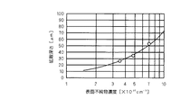
勿論、上述の傾向は、実施の形態1にかかるpinダイオードについても当てはまる。図6はn+層103の表面不純物濃度とn+層103の厚さ、即ち拡散深さとの関係を示すグラフであり、n+層103の不純物濃度勾配が2×1018cm-4に設定された場合を示している。図中○印は実測値を示す。表面不純物濃度が5×1015cm-3の場合の拡散深さは約40μmであるのに対し、表面不純物濃度1×16cm-3の場合では、拡散深さが約75μm必要である。拡散に必要な熱処理の時間は、拡散温度を1250℃とした場合、深さ40μmの拡散においては約25時間であるのに対し、深さ75μmの拡散においては約85時間である。作業者の生活リズムが1日、即ち24時間であることに鑑みれば、拡散時間はほぼ24時間程度にする事が望ましい。従って実施の形態1にかかるダイオードのようにn+層103の不純物濃度勾配が2×1018cm-4以下に設定された場合には、n+層103の表面不純物濃度は5×1015cm-3以下とし、拡散深さを40μm以下にすることが望ましい。
【0031】
なお、図7にn+層103の表面不純物濃度とスイッチング1回当たりの逆回復損失との関係もグラフとして示した。図中○印は実測値を示す。このようにn+層103の表面不純物濃度を低減することは、損失の抑制という観点からも望ましい。
【0032】
実施の形態3.
図8はpinダイオードにおいてn型半導体のカソード電極と接触する位置における不純物濃度、即ち表面不純物濃度と、そのダイオードのオン電圧との関係を示すグラフであり、図中●印は実測値を示す。n型半導体はシリコンを主成分とし、カソード電極はアルミを主成分とする場合が示されている。カソード電極に接触するn型半導体の表面不純物濃度が5×1017cm-3以上であればほぼオン電圧は3.0Vで一定となるのに対し、表面不純物濃度が5×1017cm-3未満であれば、表面不純物濃度の低下と共にオン電圧は急激に上昇する。これはカソード電極とこれに接触するn型半導体との間でのオーミックコンタクトが良好に採れるか否かの差に起因すると考えられる。従って、カソード電極に接触するn型半導体の表面不純物濃度は5×1017cm-3以上とし、良好なオーミックコンタクトを得ることが望ましい。
【0033】
しかし、実施の形態2で説明した5×1015cm-3以下という低い表面不純物濃度を有するn+層103に対してカソード電極105を直接に接触させると、良好なオーミックコンタクトが採れにくい。
【0034】
図9は本発明の実施の形態3にかかるpinダイオードの構造を示す断面図である。本発明の実施の形態1にかかるpinダイオード(図1(a)参照)に対して、n+層103とカソード電極105との間にn++層106を介在させた構造を有している。従って、n+層103の不純物濃度の内、n-型半導体基板101から最も遠い、従ってn++層106に最も近い側での値、即ちn+層103の表面不純物濃度を5×1015cm-3以下に設定しつつも、n++層106の表面不純物濃度を5×1017cm-3以上に設定することにより、n+層103の不純物濃度勾配を容易に2×1018cm-4以下に設定し、かつカソード電極105との良好なオーミックコンタクトを得ることができる。従って、逆回復動作が完了した後の電圧振幅は小さく、かつオン電圧が小さなpinダイオードを実現することができる。
【0035】
実施の形態4.
図10は本実施の形態を説明する図であり、図10(a)は図15(b)、図1(b)に対応したpinダイオードの不純物濃度プロファイルを示し、グラフ101c,102c,103cはそれぞれn-型半導体基板101、p層102、n+層103の不純物濃度プロファイルを示している。また図10(b)は逆バイアスを印加した定格電圧保持時のpinダイオードの各位置における電界強度プロファイルを示し、特にグラフE1は図10(a)と位置を整合させて示している。
【0036】
逆バイアス印加時のpinダイオードではn-型半導体基板101とp層102との間のpn接合から伸びた空乏層がn+層103にまで達しており、空乏層中において電界強度E1が大きくなっている。図10では空乏層は領域A、領域B、領域Cに跨って広がる。
【0037】
領域Bはn-型半導体基板101全体に広がり、領域Aはn-型半導体基板101と接触している位置からp層102へと部分的に進入しており、領域Dはn-型半導体基板101と接触している位置からn+層103へと部分的に進入している。そして領域Aにおける不純物量(以下、これにも符号Aを付記する)は、領域Bにおける不純物濃度(以下、これにも符号Bを付記する)と領域Dにおける不純物量(以下、これにも符号Dを付記する)との和以下になる。そして領域Aのn-型半導体基板101から遠い方の端は、不純物量Aとグラフ102cとによって、また領域Dのn-型半導体基板101から遠い方の端は、不純物量Dとグラフ103cとによって、それぞれ決定されることになる。
【0038】
安価な製造コストを実現するため、さほど微細加工プロセスを用いずに製造する大電力素子では微細な異物等が付着しても定格耐圧の低下が発生しないことが望まれる。そのための工夫として、p層102は100μm程度と、他の種類の素子に比べ、極めて厚く形成される。このように形成した素子では定格電圧保持時には、不純物量Aはp層102における不純物量の総和の、不純物量Dはn+層103における不純物量の、いずれも1/2程度となる。
【0039】
図10(b)においてグラフE1,E2は、不純物量Bの不純物量Aに対する比B/Aがそれぞれ1,2/3の場合の電界強度を示している。後者は前者よりも電界強度が屈曲する位置がp層102側に近く、pinダイオードの厚さを薄くすることができるので、オン電圧を小さくすることができる。
【0040】
図11は比B/Aと、オン電圧との関係のシミュレーション結果を示すグラフであり、B/A=1/3,2/3,3/3の値でオン電圧をシミュレーションした。B/A≦2/3ではオン電圧は比B/Aによらずにほぼ3Vの一定値を採るが、B/A>2/3ではオン電圧は比B/Aの上昇と共に急上昇する。よって比B/Aは2/3以下に設定することが望ましい。
【0041】
図12は不純物量Dの不純物量Aに対する比D/Aと、漏れ電流との関係のシミュレーション結果を示すグラフであり、比B/Aは2/3に設定している。D/A=1/3,1/2,2/2,3/2の値で漏れ電流をシミュレーションした。漏れ電流は、D/A≧2/2においてD/Aの増大に伴って急激に減少するので、比D/Aは1以上に設定することが望ましい。更には、一般に漏れ電流が10mA以下であればデバイス動作上の悪影響が無視できるので、D/A≧3/2とすることがより望ましい。
【0042】
実施の形態の変形.
上記各実施の形態ではpin構造のダイオードを例示して説明したが、pin構造を有した他の半導体素子についても適用することができる。
【0043】
図13はpin構造を有するトランジスタの構造を示す断面図である。当該トランジスタはp層402と、n+層403と、p層402及びn+層403に挟まれたn-層401と、n-層401と共にn+層403を挟むp+層404と、n+層403と共にn-層401を挟む電極405と、n-層401と共にp層402を挟む電極406と、n+層403と共にp+層404を挟む電極407とを備えている。電極405,406,407はそれぞれベース電極、エミッタ電極、コレクタ電極として機能する。
【0044】
当該トランジスタは、そのp層402、n-層401、n+層403において、pin構造を有しており、実施の形態1乃至実施の形態4に示された技術を適用し、ターンオフ時の電圧振動を抑制することができる。
【0045】
図14はpin構造を有するGCTサイリスタの構造を示す断面図である。当該GCTサイリスタは、p層502と、n+層503と、p層502及びn+層503に挟まれたn-層501と、n-層501と共にn+層503を挟むp+層504と、n-層501と共にp層502を挟むn層505と、p層502と共にn層505を挟む電極506と、n-層501と共にp層502を挟む電極507と、n+層503と共にp+層504を挟む電極508とを備えている。電極506,507,508はそれぞれカソード電極、ゲート電極、アノード電極として機能する。当該サイリスタは、そのp層502、n-層501、n+層503においてpin構造を有しており、実施の形態1乃至実施の形態4に示された技術を適用し、逆回復動作時の電圧振動を抑制することができる。
【0046】
【発明の効果】
この発明のうち請求項1にかかる半導体装置によれば、第2半導体層の不純物濃度勾配が緩やかであるので、第1半導体層と半導体基板とが作るpn接合を有するダイオードの逆回復動作時や、あるいは当該pn接合を有するトランジスタやGCTサイリスタのターンオフ動作時の空乏層の急激な広がりを抑制する。従って上記動作時の不要な電圧変動の発生、即ちノイズの発生を抑制することができる。また上記不純物濃度勾配を容易に得ることができる。
【0048】
この発明のうち請求項2にかかる半導体装置によれば、第2半導体層の不純物濃度の最大値を抑制してその不純物濃度勾配を容易に良好にしつつも、不純物濃度の高い第3半導体層が介在することにより、金属電極と第2半導体層との良好なオーミックコンタクトを得ることができる。
【図面の簡単な説明】
【図1】 この発明の実施の形態1にかかるダイオードの構造を示す断面図及び濃度プロファイルである。
【図2】 この発明の実施の形態1にかかるダイオードの動作を示すグラフである。
【図3】 この発明の実施の形態1にかかるダイオードの動作を示すグラフである。
【図4】 この発明の実施の形態1を説明するグラフである。
【図5】 この発明の実施の形態2を説明する濃度プロファイルである。
【図6】 この発明の実施の形態2を説明するグラフである。
【図7】 この発明の実施の形態2を説明するグラフである。
【図8】 この発明の実施の形態3を説明するグラフである。
【図9】 この発明の実施の形態3にかかるダイオードの構造を示す断面図である。
【図10】 この発明の実施の形態4を説明する濃度プロファイル及び電界強度プロファイルである。
【図11】 この発明の実施の形態4を説明するグラフである。
【図12】 この発明の実施の形態4を説明するグラフである。
【図13】 この発明の変形の構造を示す断面図である。
【図14】 この発明の変形の構造を示す断面図である。
【図15】 従来の技術にかかるダイオードの構造を示す断面図及び濃度プロファイルである。
【図16】 従来の技術にかかるダイオードの動作を示すグラフである。
【符号の説明】
101 n-型半導体基板、401,501 n-層、102,402,502p層、103,403,503 n+層、106 n++層、A,B,D 領域及び不純物量。[0001]
BACKGROUND OF THE INVENTION
The present invention relates to a semiconductor device having a pin structure, such as a diode, a transistor, and a thyristor.
[0002]
[Prior art]
15A and 15B show the structure of a conventional pin diode. FIG. 15A is a cross-sectional view and FIG. 15B is an impurity concentration profile. For example, an n −
[0003]
The impurities of the n −
[0004]
In general, when a reverse bias is applied to a diode having a pn junction from a state in which a current flows in the forward direction by instantaneous switching of an external circuit, a large reverse current flows transiently for a certain period. This is because the diode has a minority carrier accumulation phenomenon and does not immediately recover in the reverse direction once the current becomes zero. This reverse current continues until the fractional carriers remaining as excess carriers near the junction are reduced below a certain concentration and a depletion layer is established.
[0005]
When the depletion layer is established, this starts to support the reverse voltage, and the reverse voltage gradually increases and the reverse current gradually decreases in accordance with the spread of the depletion layer. Then, the element voltage is constantly equal to the voltage applied to the reverse bias, and the reverse recovery operation is completed. The reverse current that flows in the reverse recovery operation decreases at a current decrease rate determined by the reverse bias value and the inductance of the external circuit.
[0006]
In the diode shown in FIG. 15, the center of carrier recombination is formed near the pn junction formed by the
[0007]
[Problems to be solved by the invention]
However, when the reverse bias voltage is high, there is a problem that the applied voltage of the diode abruptly vibrates in the vicinity of the completion of the reverse recovery operation, thereby generating noise that causes malfunction of peripheral electrical equipment. FIG. 16 is a graph showing temporal changes in the voltage V A and the current I A before and after the reverse recovery operation of the diode shown in FIG. 15, and the time when switching from the forward bias to the reverse bias by the external circuit is zero. . It can be seen that at about 8 μs after switching, the diode current starts to constantly become zero, and immediately after that, voltage oscillation of amplitude ΔV exceeding 2000 V occurs.
[0008]
Such voltage oscillation is considered to be caused by resonance of the LCR series circuit formed by the diode and the external circuit. This LCR series circuit includes a capacitance component C that uses the depletion layer and excess carriers of the diode as parameters, a resistance component R that uses the applied voltage, leakage current, and excess carrier recombination current as parameters, and an inductance component of the external circuit. And L.
[0009]
The capacitance component C and the resistance component R of the diode change with time. In particular, the resistance component R changes abruptly when excess carriers outside the depletion layer disappear. Therefore, it is considered that the resonance condition of the LCR circuit is reached and the voltage oscillates as shown in FIG. Further, when the depletion layer reaches the n + layer 603, the capacitance component C changes abruptly, and this may trigger a voltage oscillation.
[0010]
Such a voltage oscillation is not limited to the diode, but may occur when the voltage is increased in the turn-off operation even in a GCT (gate controlled turn-off) thyristor having a high switching speed. Such voltage oscillation has a problem of causing noise that causes malfunction of peripheral electrical devices.
[0011]
The present invention has been made to solve the above-described problems, and an object of the present invention is to provide a semiconductor device in which the applied voltage generates less vibration during the reverse recovery operation and the turn-off operation.
[0012]
A technique for controlling the semiconductor layer and the concentration in order to improve the waveform at the time of reverse recovery is disclosed in, for example, Japanese Patent Application Laid-Open No. 62-115880.
[0013]
[Means for Solving the Problems]
According to a first aspect of the present invention, there is provided a first semiconductor layer of a first conductivity type, a second semiconductor layer of a second conductivity type, and interposed between the first semiconductor layer and the second semiconductor layer. A semiconductor substrate having a second conductivity type semiconductor substrate having an impurity concentration lower than that of the second semiconductor layer, wherein the impurity concentration of the second semiconductor layer decreases as the semiconductor substrate approaches, The impurity concentration gradient that decreases from 90% to 50% of the maximum value of the impurity concentration in the semiconductor layer is 1 × 10 18 cm −4 or more and 2 × 10 18 cm −4 or less, and the second semiconductor layer has the above-mentioned The maximum value of the impurity concentration is 1 × 10 15 cm −3 or more and 5 × 10 15 cm −3 or less.
[0015]
According to a second aspect of the present invention, there is provided the semiconductor device according to the first aspect, wherein the second conductive type third semiconductor layer sandwiching the second semiconductor layer together with the semiconductor substrate, and the second A metal electrode sandwiching the third semiconductor layer together with the semiconductor layer, and the surface impurity concentration of the third semiconductor layer on the metal electrode side is less than or equal to the maximum solid solubility of the impurity in the third semiconductor layer, × 10 17 cm -3 or more
[0019]
DETAILED DESCRIPTION OF THE INVENTION
Embodiment 1 FIG.
1A and 1B show the structure of a pin diode according to a first embodiment of the present invention, where FIG. 1A is a cross-sectional view and FIG. 1B is an impurity concentration profile. For example, an n −
[0020]
In the vicinity of the pn junction formed by the
[0021]
Impurities of the n −
[0022]
However, unlike the diode shown in FIG. 15, the impurity concentration gradient of the n + layer 103 is set to 2 × 10 18 cm −4 or less.
[0023]
2 and 3 are graphs showing temporal changes in the voltage V A and the current I A before and after the reverse recovery operation of the diode shown in FIG. 1, and the time when the external circuit switches from the forward bias to the reverse bias. Is zero. 2 and 3 show cases where the impurity concentration gradient of the n + layer 103 is set to 2 × 10 18 cm −4 and 9 × 10 17 cm −4 , respectively. The distance between them, the total amount of impurities introduced into the n + layer 103, the thickness of the
[0024]
In both FIGS. 2 and 3, at about 8 μs after switching, the current of the diode starts to constantly become zero, and voltage oscillation occurs immediately after that. However, in FIG. 2, the amplitude ΔV is about several hundreds V, which is significantly suppressed to about 1/5 as compared with the case shown in FIG. In the case shown in FIG. 3, the amplitude ΔV is further suppressed. If the amplitude ΔV is 500 V or less, the external circuit is not easily affected by noise, so the impurity concentration gradient of the n + layer 103 is desirably set to 2 × 10 18 cm −4 or less.
[0025]
FIG. 4 is a graph showing the relationship between the impurity concentration gradient of the n + layer 103 and the amplitude ΔV of the voltage oscillation during the reverse recovery operation. It can be seen that voltage oscillation during the reverse recovery operation is reduced by making the impurity concentration gradient of the n + layer 103 gentle. This is considered to be due to the fact that when the depletion layer extending from the pn junction reaches the n + layer 103 during the reverse recovery operation, the depletion layer does not stop expanding more rapidly as the impurity concentration gradient of the n + layer 103 is smaller. It is done.
[0026]
In forming the n + layer 103, phosphorus, arsenic or the like is usually deposited on the n −
[0027]
FIG. 5 is an impurity concentration profile of the pin diode corresponding to FIGS. 15 (b) and 1 (b). In the drawing,
[0028]
[0029]
As described above, in the formation of the n + layer 103, phosphorus, arsenic, or the like is usually deposited on the n −
[0030]
Of course, the above-mentioned tendency is also applied to the pin diode according to the first embodiment. Figure 6 is the thickness of the surface impurity concentration and the n + layer 103 of the n + layer 103, that is, a graph showing the relationship between the diffusion depth, the impurity concentration gradient of the n + layer 103 is set to 2 × 10 18 cm -4 Shows the case. In the figure, ○ marks indicate actual measurement values. When the surface impurity concentration is 5 × 10 15 cm −3 , the diffusion depth is about 40 μm, whereas when the surface impurity concentration is 1 × 16 cm −3 , the diffusion depth is about 75 μm. When the diffusion temperature is 1250 ° C., the heat treatment time required for the diffusion is about 25 hours for the diffusion at a depth of 40 μm, and about 85 hours for the diffusion at a depth of 75 μm. Considering that the life rhythm of the worker is one day, that is, 24 hours, it is desirable that the diffusion time is about 24 hours. Therefore, when the impurity concentration gradient of the n + layer 103 like a diode according to the first embodiment is set to 2 × 10 18 cm -4 or less, the surface impurity concentration of 5 × 10 the n + layer 103 15 cm -3 or less and the diffusion depth is preferably 40 μm or less.
[0031]
FIG. 7 also shows a graph of the relationship between the surface impurity concentration of the n + layer 103 and the reverse recovery loss per switching. In the figure, ○ marks indicate actual measurement values. Thus, reducing the surface impurity concentration of the n + layer 103 is desirable also from the viewpoint of suppressing loss.
[0032]
FIG. 8 is a graph showing the relationship between the impurity concentration at the position in contact with the cathode electrode of the n-type semiconductor in the pin diode, that is, the surface impurity concentration, and the ON voltage of the diode. The case where the n-type semiconductor is mainly composed of silicon and the cathode electrode is mainly composed of aluminum is shown. If the surface impurity concentration of the n-type semiconductor in contact with the cathode electrode is 5 × 10 17 cm −3 or more, the on-state voltage is almost constant at 3.0 V, whereas the surface impurity concentration is 5 × 10 17 cm −3. If it is less than that, the on-state voltage increases rapidly as the surface impurity concentration decreases. This is considered to be caused by the difference in whether or not the ohmic contact between the cathode electrode and the n-type semiconductor in contact with the cathode electrode can be satisfactorily taken. Therefore, it is desirable to obtain a good ohmic contact by setting the surface impurity concentration of the n-type semiconductor in contact with the cathode electrode to 5 × 10 17 cm −3 or more.
[0033]
However, when the
[0034]
FIG. 9 is a sectional view showing the structure of a pin diode according to the third embodiment of the present invention. The pin diode according to the first embodiment of the present invention (see FIG. 1A) has a structure in which an n ++ layer 106 is interposed between an n + layer 103 and a
[0035]
FIG. 10 is a diagram for explaining the present embodiment. FIG. 10 (a) shows the impurity concentration profile of the pin diode corresponding to FIGS. 15 (b) and 1 (b), and
[0036]
In the pin diode when reverse bias is applied, the depletion layer extending from the pn junction between the n −
[0037]
Region B extends over the entire n −
[0038]
In order to realize an inexpensive manufacturing cost, it is desired that a high power element manufactured without using a microfabrication process does not cause a decrease in rated withstand voltage even if fine foreign matters adhere. As a device for that purpose, the
[0039]
In FIG. 10B, graphs E1 and E2 indicate the electric field strengths when the ratio B / A of the impurity amount B to the impurity amount A is 1/3, respectively. In the latter, the position where the electric field strength is bent is closer to the p-
[0040]
FIG. 11 is a graph showing a simulation result of the relationship between the ratio B / A and the on-voltage. The on-voltage was simulated with values of B / A = 1/3, 2/3, and 3/3. When B / A ≦ 2/3, the on-state voltage takes a constant value of about 3 V regardless of the ratio B / A. However, when B / A> 2/3, the on-state voltage increases rapidly as the ratio B / A increases. Therefore, the ratio B / A is desirably set to 2/3 or less.
[0041]
FIG. 12 is a graph showing a simulation result of the relationship between the ratio D / A of the impurity amount D to the impurity amount A and the leakage current, and the ratio B / A is set to 2/3. The leakage current was simulated with values of D / A = 1/3, 1/2, 2/2, and 3/2. Since the leakage current rapidly decreases as D / A increases when D / A ≧ 2/2, the ratio D / A is desirably set to 1 or more. Furthermore, since the adverse effect on device operation can generally be ignored if the leakage current is 10 mA or less, it is more desirable that D / A ≧ 3/2.
[0042]
Modification of the embodiment.
In each of the above embodiments, a pin structure diode has been described as an example. However, the present invention can also be applied to other semiconductor elements having a pin structure.
[0043]
FIG. 13 is a cross-sectional view illustrating a structure of a transistor having a pin structure. The transistor includes
[0044]
The transistor has a pin structure in the
[0045]
FIG. 14 is a sectional view showing the structure of a GCT thyristor having a pin structure. The GCT thyristor includes
[0046]
【The invention's effect】
According to the semiconductor device of the first aspect of the present invention, since the impurity concentration gradient of the second semiconductor layer is gentle, during the reverse recovery operation of the diode having the pn junction formed by the first semiconductor layer and the semiconductor substrate, Alternatively, the rapid expansion of the depletion layer during the turn-off operation of the transistor having the pn junction or the GCT thyristor is suppressed. Therefore, it is possible to suppress the occurrence of unnecessary voltage fluctuations during the operation, that is, the generation of noise. Moreover, the impurity concentration gradient can be easily obtained.
[0048]
According to the semiconductor device of the second aspect of the present invention, the third semiconductor layer having a high impurity concentration can be obtained while suppressing the maximum value of the impurity concentration of the second semiconductor layer to easily improve the impurity concentration gradient. By interposing, a good ohmic contact between the metal electrode and the second semiconductor layer can be obtained.
[Brief description of the drawings]
FIG. 1 is a cross-sectional view and a concentration profile showing a structure of a diode according to a first embodiment of the present invention.
FIG. 2 is a graph showing the operation of the diode according to the first embodiment of the present invention;
FIG. 3 is a graph showing the operation of the diode according to the first embodiment of the present invention;
FIG. 4 is a graph illustrating Embodiment 1 of the present invention.
FIG. 5 is a density
FIG. 6 is a
FIG. 7 is a
FIG. 8 is a
FIG. 9 is a sectional view showing a structure of a diode according to a third embodiment of the present invention.
FIG. 10 shows a concentration profile and an electric field strength profile for explaining the fourth embodiment of the present invention.
FIG. 11 is a
FIG. 12 is a
FIG. 13 is a cross-sectional view showing a modified structure of the present invention.
FIG. 14 is a cross-sectional view showing a modified structure of the present invention.
FIG. 15 is a cross-sectional view and a concentration profile showing a structure of a diode according to a conventional technique.
FIG. 16 is a graph showing the operation of a diode according to a conventional technique.
[Explanation of symbols]
101 n − type semiconductor substrate, 401, 501 n − layer, 102, 402, 502p layer, 103, 403, 503 n + layer, 106 n ++ layer, A, B, D region and impurity amount.
Claims (2)
前記第2半導体層の不純物濃度は前記半導体基板に近づくにつれて減少し、前記第2半導体層における前記不純物濃度の最大値の90%から50%へと減少する不純物濃度勾配が、1×10 18 cm -4 以上2×1018cm-4以下であり、前記第2半導体層の前記不純物濃度の前記最大値は1×10 15 cm -3 以上5×1015cm-3以下であることを特徴とする半導体装置。An impurity concentration lower than that of the second semiconductor layer is interposed between the first semiconductor layer of the first conductivity type, the second semiconductor layer of the second conductivity type, and the first semiconductor layer and the second semiconductor layer. A semiconductor substrate of the second conductivity type,
The impurity concentration of the second semiconductor layer decreases as it approaches the semiconductor substrate, and an impurity concentration gradient that decreases from 90% to 50% of the maximum value of the impurity concentration in the second semiconductor layer is 1 × 10 18 cm. -4 or more and 2 × 10 18 cm −4 or less, and the maximum value of the impurity concentration of the second semiconductor layer is 1 × 10 15 cm −3 or more and 5 × 10 15 cm −3 or less. Semiconductor device.
前記第2半導体層と共に前記第3半導体層を挟む金属電極と
を更に備え、
前記第3半導体層の前記金属電極側の表面不純物濃度が前記第3半導体層における当該不純物の最大固溶度以下であって5×1017cm-3以上であることを特徴とする請求項1記載の半導体装置。A third semiconductor layer of the second conductivity type sandwiching the second semiconductor layer together with the semiconductor substrate;
A metal electrode sandwiching the third semiconductor layer together with the second semiconductor layer,
The surface impurity concentration of the third semiconductor layer on the metal electrode side is not more than the maximum solid solubility of the impurity in the third semiconductor layer and not less than 5 × 10 17 cm −3. The semiconductor device described.
Priority Applications (4)
| Application Number | Priority Date | Filing Date | Title |
|---|---|---|---|
| JP30530399A JP4129106B2 (en) | 1999-10-27 | 1999-10-27 | Semiconductor device |
| US09/544,290 US6614087B1 (en) | 1999-10-27 | 2000-04-06 | Semiconductor device |
| DE60041030T DE60041030D1 (en) | 1999-10-27 | 2000-06-29 | Semiconductor device |
| EP00113802A EP1096576B1 (en) | 1999-10-27 | 2000-06-29 | Semiconductor device |
Applications Claiming Priority (1)
| Application Number | Priority Date | Filing Date | Title |
|---|---|---|---|
| JP30530399A JP4129106B2 (en) | 1999-10-27 | 1999-10-27 | Semiconductor device |
Related Child Applications (1)
| Application Number | Title | Priority Date | Filing Date |
|---|---|---|---|
| JP2006060754A Division JP2006157057A (en) | 2006-03-07 | 2006-03-07 | Semiconductor device |
Publications (3)
| Publication Number | Publication Date |
|---|---|
| JP2001127308A JP2001127308A (en) | 2001-05-11 |
| JP2001127308A5 JP2001127308A5 (en) | 2005-07-14 |
| JP4129106B2 true JP4129106B2 (en) | 2008-08-06 |
Family
ID=17943486
Family Applications (1)
| Application Number | Title | Priority Date | Filing Date |
|---|---|---|---|
| JP30530399A Expired - Fee Related JP4129106B2 (en) | 1999-10-27 | 1999-10-27 | Semiconductor device |
Country Status (4)
| Country | Link |
|---|---|
| US (1) | US6614087B1 (en) |
| EP (1) | EP1096576B1 (en) |
| JP (1) | JP4129106B2 (en) |
| DE (1) | DE60041030D1 (en) |
Families Citing this family (10)
| Publication number | Priority date | Publication date | Assignee | Title |
|---|---|---|---|---|
| JP5272299B2 (en) * | 2005-11-10 | 2013-08-28 | 富士電機株式会社 | Semiconductor device and manufacturing method thereof |
| WO2007055352A1 (en) | 2005-11-14 | 2007-05-18 | Fuji Electric Device Technology Co., Ltd. | Semiconductor device and method for manufacturing same |
| DE102007028316B3 (en) | 2007-06-20 | 2008-10-30 | Semikron Elektronik Gmbh & Co. Kg | Semiconductor device with buffer layer and method for its production |
| WO2014199465A1 (en) * | 2013-06-12 | 2014-12-18 | 三菱電機株式会社 | Semiconductor apparatus |
| JP2016195271A (en) * | 2016-07-04 | 2016-11-17 | 三菱電機株式会社 | Semiconductor device |
| JP7243956B2 (en) * | 2018-03-23 | 2023-03-22 | 新電元工業株式会社 | Semiconductor device, method for manufacturing semiconductor device, and power conversion circuit |
| CN110504167A (en) * | 2018-05-17 | 2019-11-26 | 上海先进半导体制造股份有限公司 | Insulated gate bipolar transistor and its manufacturing method |
| DE102018213633A1 (en) | 2018-08-13 | 2020-02-13 | Infineon Technologies Ag | Semiconductor device |
| DE102018213635B4 (en) * | 2018-08-13 | 2020-11-05 | Infineon Technologies Ag | Semiconductor device |
| DE102021000610A1 (en) * | 2021-02-08 | 2022-08-11 | 3-5 Power Electronics GmbH | Stacked III-V semiconductor diode |
Family Cites Families (11)
| Publication number | Priority date | Publication date | Assignee | Title |
|---|---|---|---|---|
| FR2252652B1 (en) | 1973-11-28 | 1977-06-10 | Silec Semi Conducteurs | |
| US4101920A (en) | 1975-01-29 | 1978-07-18 | Sony Corporation | Green light emitting diode |
| US4038106A (en) | 1975-04-30 | 1977-07-26 | Rca Corporation | Four-layer trapatt diode and method for making same |
| JPS5942989B2 (en) * | 1977-01-24 | 1984-10-18 | 株式会社日立製作所 | High voltage semiconductor device and its manufacturing method |
| DE3531631A1 (en) * | 1985-09-05 | 1987-03-05 | Licentia Gmbh | ASYMMETRIC THYRISTOR AND METHOD FOR THE PRODUCTION THEREOF |
| EP0283788A1 (en) | 1987-03-09 | 1988-09-28 | Siemens Aktiengesellschaft | Turn off semiconductor power device |
| US4980315A (en) | 1988-07-18 | 1990-12-25 | General Instrument Corporation | Method of making a passivated P-N junction in mesa semiconductor structure |
| FR2638892B1 (en) | 1988-11-09 | 1992-12-24 | Sgs Thomson Microelectronics | METHOD FOR MODULATING THE QUANTITY OF GOLD DIFFUSED IN A SILICON SUBSTRATE AND RAPID DIODE OBTAINED BY THIS PROCESS |
| JP3994443B2 (en) | 1995-05-18 | 2007-10-17 | 三菱電機株式会社 | Diode and manufacturing method thereof |
| JPH09252153A (en) * | 1996-01-09 | 1997-09-22 | Japan Energy Corp | Gunn diode |
| DE19713962C1 (en) * | 1997-04-04 | 1998-07-02 | Siemens Ag | Power diode with charge coupling zones for freewheeling diode or voltage boundary controller |
-
1999
- 1999-10-27 JP JP30530399A patent/JP4129106B2/en not_active Expired - Fee Related
-
2000
- 2000-04-06 US US09/544,290 patent/US6614087B1/en not_active Expired - Lifetime
- 2000-06-29 EP EP00113802A patent/EP1096576B1/en not_active Expired - Lifetime
- 2000-06-29 DE DE60041030T patent/DE60041030D1/en not_active Expired - Lifetime
Also Published As
| Publication number | Publication date |
|---|---|
| EP1096576B1 (en) | 2008-12-10 |
| EP1096576A1 (en) | 2001-05-02 |
| DE60041030D1 (en) | 2009-01-22 |
| US6614087B1 (en) | 2003-09-02 |
| JP2001127308A (en) | 2001-05-11 |
Similar Documents
| Publication | Publication Date | Title |
|---|---|---|
| JP5374883B2 (en) | Semiconductor device and manufacturing method thereof | |
| US9263529B2 (en) | Semiconductor device with vertically inhomogeneous heavy metal doping profile | |
| JP3906076B2 (en) | Semiconductor device | |
| US7768101B2 (en) | Semiconductor device having an insulated gate bipolar transistor and a free wheel diode | |
| JP6676988B2 (en) | Semiconductor device | |
| US8829519B2 (en) | Semiconductor device | |
| JPH09121052A (en) | Semiconductor device and fabrication thereof | |
| WO2015072064A1 (en) | Insulated gate bipolar transistor and method for manufacturing same | |
| JP2000323488A (en) | Diode and manufacture thereof | |
| JP4653273B2 (en) | Semiconductor device and manufacturing method thereof | |
| JP4129106B2 (en) | Semiconductor device | |
| US9209027B1 (en) | Adjusting the charge carrier lifetime in a bipolar semiconductor device | |
| JP2020077720A (en) | Silicon carbide semiconductor device and method of manufacturing silicon carbide semiconductor device | |
| JP4123913B2 (en) | Manufacturing method of semiconductor device | |
| JPH07226405A (en) | Manufacture of semiconductor device | |
| JP2016015392A (en) | Semiconductor device and power conversion system using the same | |
| US9349799B2 (en) | Adjusting the charge carrier lifetime in a bipolar semiconductor device | |
| JP2002261281A (en) | Manufacturing method of insulated gate bipolar transistor | |
| JP2851026B2 (en) | High speed diode | |
| JP2006245475A (en) | Semiconductor device and its manufacturing method | |
| JP3673334B2 (en) | Semiconductor diode | |
| JP2008263217A (en) | Semiconductor device | |
| US6218683B1 (en) | Diode | |
| JP2004088012A (en) | Diode | |
| JP2006157057A (en) | Semiconductor device |
Legal Events
| Date | Code | Title | Description |
|---|---|---|---|
| A521 | Written amendment |
Free format text: JAPANESE INTERMEDIATE CODE: A523 Effective date: 20041124 |
|
| A621 | Written request for application examination |
Free format text: JAPANESE INTERMEDIATE CODE: A621 Effective date: 20041124 |
|
| A977 | Report on retrieval |
Free format text: JAPANESE INTERMEDIATE CODE: A971007 Effective date: 20060118 |
|
| A131 | Notification of reasons for refusal |
Free format text: JAPANESE INTERMEDIATE CODE: A131 Effective date: 20060124 |
|
| A521 | Written amendment |
Free format text: JAPANESE INTERMEDIATE CODE: A523 Effective date: 20060307 |
|
| A131 | Notification of reasons for refusal |
Free format text: JAPANESE INTERMEDIATE CODE: A131 Effective date: 20070612 |
|
| A521 | Written amendment |
Free format text: JAPANESE INTERMEDIATE CODE: A523 Effective date: 20070809 |
|
| RD04 | Notification of resignation of power of attorney |
Free format text: JAPANESE INTERMEDIATE CODE: A7424 Effective date: 20070809 |
|
| TRDD | Decision of grant or rejection written | ||
| A01 | Written decision to grant a patent or to grant a registration (utility model) |
Free format text: JAPANESE INTERMEDIATE CODE: A01 Effective date: 20080430 |
|
| A01 | Written decision to grant a patent or to grant a registration (utility model) |
Free format text: JAPANESE INTERMEDIATE CODE: A01 |
|
| A61 | First payment of annual fees (during grant procedure) |
Free format text: JAPANESE INTERMEDIATE CODE: A61 Effective date: 20080516 |
|
| FPAY | Renewal fee payment (event date is renewal date of database) |
Free format text: PAYMENT UNTIL: 20110523 Year of fee payment: 3 |
|
| R150 | Certificate of patent or registration of utility model |
Ref document number: 4129106 Country of ref document: JP Free format text: JAPANESE INTERMEDIATE CODE: R150 Free format text: JAPANESE INTERMEDIATE CODE: R150 |
|
| FPAY | Renewal fee payment (event date is renewal date of database) |
Free format text: PAYMENT UNTIL: 20110523 Year of fee payment: 3 |
|
| FPAY | Renewal fee payment (event date is renewal date of database) |
Free format text: PAYMENT UNTIL: 20120523 Year of fee payment: 4 |
|
| FPAY | Renewal fee payment (event date is renewal date of database) |
Free format text: PAYMENT UNTIL: 20120523 Year of fee payment: 4 |
|
| FPAY | Renewal fee payment (event date is renewal date of database) |
Free format text: PAYMENT UNTIL: 20130523 Year of fee payment: 5 |
|
| FPAY | Renewal fee payment (event date is renewal date of database) |
Free format text: PAYMENT UNTIL: 20140523 Year of fee payment: 6 |
|
| R250 | Receipt of annual fees |
Free format text: JAPANESE INTERMEDIATE CODE: R250 |
|
| R250 | Receipt of annual fees |
Free format text: JAPANESE INTERMEDIATE CODE: R250 |
|
| R250 | Receipt of annual fees |
Free format text: JAPANESE INTERMEDIATE CODE: R250 |
|
| LAPS | Cancellation because of no payment of annual fees |