JP4119608B2 - Sealed package and method for packaging electronic circuit module - Google Patents
Sealed package and method for packaging electronic circuit module Download PDFInfo
- Publication number
- JP4119608B2 JP4119608B2 JP2000544170A JP2000544170A JP4119608B2 JP 4119608 B2 JP4119608 B2 JP 4119608B2 JP 2000544170 A JP2000544170 A JP 2000544170A JP 2000544170 A JP2000544170 A JP 2000544170A JP 4119608 B2 JP4119608 B2 JP 4119608B2
- Authority
- JP
- Japan
- Prior art keywords
- chamber
- circuit module
- package
- compare
- disposed
- Prior art date
- Legal status (The legal status is an assumption and is not a legal conclusion. Google has not performed a legal analysis and makes no representation as to the accuracy of the status listed.)
- Expired - Fee Related
Links
Images


Classifications
-
- H—ELECTRICITY
- H05—ELECTRIC TECHNIQUES NOT OTHERWISE PROVIDED FOR
- H05K—PRINTED CIRCUITS; CASINGS OR CONSTRUCTIONAL DETAILS OF ELECTRIC APPARATUS; MANUFACTURE OF ASSEMBLAGES OF ELECTRICAL COMPONENTS
- H05K5/00—Casings, cabinets or drawers for electric apparatus
- H05K5/06—Hermetically-sealed casings
- H05K5/064—Hermetically-sealed casings sealed by potting, e.g. waterproof resin poured in a rigid casing
-
- B—PERFORMING OPERATIONS; TRANSPORTING
- B60—VEHICLES IN GENERAL
- B60C—VEHICLE TYRES; TYRE INFLATION; TYRE CHANGING; CONNECTING VALVES TO INFLATABLE ELASTIC BODIES IN GENERAL; DEVICES OR ARRANGEMENTS RELATED TO TYRES
- B60C23/00—Devices for measuring, signalling, controlling, or distributing tyre pressure or temperature, specially adapted for mounting on vehicles; Arrangement of tyre inflating devices on vehicles, e.g. of pumps or of tanks; Tyre cooling arrangements
- B60C23/02—Signalling devices actuated by tyre pressure
- B60C23/04—Signalling devices actuated by tyre pressure mounted on the wheel or tyre
- B60C23/0491—Constructional details of means for attaching the control device
- B60C23/0493—Constructional details of means for attaching the control device for attachment on the tyre
-
- G—PHYSICS
- G06—COMPUTING; CALCULATING OR COUNTING
- G06K—GRAPHICAL DATA READING; PRESENTATION OF DATA; RECORD CARRIERS; HANDLING RECORD CARRIERS
- G06K19/00—Record carriers for use with machines and with at least a part designed to carry digital markings
- G06K19/04—Record carriers for use with machines and with at least a part designed to carry digital markings characterised by the shape
- G06K19/041—Constructional details
-
- G—PHYSICS
- G06—COMPUTING; CALCULATING OR COUNTING
- G06K—GRAPHICAL DATA READING; PRESENTATION OF DATA; RECORD CARRIERS; HANDLING RECORD CARRIERS
- G06K19/00—Record carriers for use with machines and with at least a part designed to carry digital markings
- G06K19/06—Record carriers for use with machines and with at least a part designed to carry digital markings characterised by the kind of the digital marking, e.g. shape, nature, code
- G06K19/067—Record carriers with conductive marks, printed circuits or semiconductor circuit elements, e.g. credit or identity cards also with resonating or responding marks without active components
- G06K19/07—Record carriers with conductive marks, printed circuits or semiconductor circuit elements, e.g. credit or identity cards also with resonating or responding marks without active components with integrated circuit chips
- G06K19/077—Constructional details, e.g. mounting of circuits in the carrier
- G06K19/07749—Constructional details, e.g. mounting of circuits in the carrier the record carrier being capable of non-contact communication, e.g. constructional details of the antenna of a non-contact smart card
- G06K19/07758—Constructional details, e.g. mounting of circuits in the carrier the record carrier being capable of non-contact communication, e.g. constructional details of the antenna of a non-contact smart card arrangements for adhering the record carrier to further objects or living beings, functioning as an identification tag
- G06K19/07764—Constructional details, e.g. mounting of circuits in the carrier the record carrier being capable of non-contact communication, e.g. constructional details of the antenna of a non-contact smart card arrangements for adhering the record carrier to further objects or living beings, functioning as an identification tag the adhering arrangement making the record carrier attachable to a tire
-
- H—ELECTRICITY
- H05—ELECTRIC TECHNIQUES NOT OTHERWISE PROVIDED FOR
- H05K—PRINTED CIRCUITS; CASINGS OR CONSTRUCTIONAL DETAILS OF ELECTRIC APPARATUS; MANUFACTURE OF ASSEMBLAGES OF ELECTRICAL COMPONENTS
- H05K3/00—Apparatus or processes for manufacturing printed circuits
- H05K3/22—Secondary treatment of printed circuits
- H05K3/28—Applying non-metallic protective coatings
- H05K3/284—Applying non-metallic protective coatings for encapsulating mounted components
-
- H—ELECTRICITY
- H01—ELECTRIC ELEMENTS
- H01L—SEMICONDUCTOR DEVICES NOT COVERED BY CLASS H10
- H01L2224/00—Indexing scheme for arrangements for connecting or disconnecting semiconductor or solid-state bodies and methods related thereto as covered by H01L24/00
- H01L2224/01—Means for bonding being attached to, or being formed on, the surface to be connected, e.g. chip-to-package, die-attach, "first-level" interconnects; Manufacturing methods related thereto
- H01L2224/02—Bonding areas; Manufacturing methods related thereto
- H01L2224/04—Structure, shape, material or disposition of the bonding areas prior to the connecting process
- H01L2224/05—Structure, shape, material or disposition of the bonding areas prior to the connecting process of an individual bonding area
- H01L2224/0554—External layer
- H01L2224/0555—Shape
- H01L2224/05552—Shape in top view
- H01L2224/05554—Shape in top view being square
-
- H—ELECTRICITY
- H01—ELECTRIC ELEMENTS
- H01L—SEMICONDUCTOR DEVICES NOT COVERED BY CLASS H10
- H01L2224/00—Indexing scheme for arrangements for connecting or disconnecting semiconductor or solid-state bodies and methods related thereto as covered by H01L24/00
- H01L2224/01—Means for bonding being attached to, or being formed on, the surface to be connected, e.g. chip-to-package, die-attach, "first-level" interconnects; Manufacturing methods related thereto
- H01L2224/26—Layer connectors, e.g. plate connectors, solder or adhesive layers; Manufacturing methods related thereto
- H01L2224/31—Structure, shape, material or disposition of the layer connectors after the connecting process
- H01L2224/32—Structure, shape, material or disposition of the layer connectors after the connecting process of an individual layer connector
- H01L2224/321—Disposition
- H01L2224/32151—Disposition the layer connector connecting between a semiconductor or solid-state body and an item not being a semiconductor or solid-state body, e.g. chip-to-substrate, chip-to-passive
- H01L2224/32221—Disposition the layer connector connecting between a semiconductor or solid-state body and an item not being a semiconductor or solid-state body, e.g. chip-to-substrate, chip-to-passive the body and the item being stacked
- H01L2224/32225—Disposition the layer connector connecting between a semiconductor or solid-state body and an item not being a semiconductor or solid-state body, e.g. chip-to-substrate, chip-to-passive the body and the item being stacked the item being non-metallic, e.g. insulating substrate with or without metallisation
-
- H—ELECTRICITY
- H01—ELECTRIC ELEMENTS
- H01L—SEMICONDUCTOR DEVICES NOT COVERED BY CLASS H10
- H01L2224/00—Indexing scheme for arrangements for connecting or disconnecting semiconductor or solid-state bodies and methods related thereto as covered by H01L24/00
- H01L2224/01—Means for bonding being attached to, or being formed on, the surface to be connected, e.g. chip-to-package, die-attach, "first-level" interconnects; Manufacturing methods related thereto
- H01L2224/42—Wire connectors; Manufacturing methods related thereto
- H01L2224/47—Structure, shape, material or disposition of the wire connectors after the connecting process
- H01L2224/48—Structure, shape, material or disposition of the wire connectors after the connecting process of an individual wire connector
- H01L2224/4805—Shape
- H01L2224/4809—Loop shape
- H01L2224/48091—Arched
-
- H—ELECTRICITY
- H01—ELECTRIC ELEMENTS
- H01L—SEMICONDUCTOR DEVICES NOT COVERED BY CLASS H10
- H01L2224/00—Indexing scheme for arrangements for connecting or disconnecting semiconductor or solid-state bodies and methods related thereto as covered by H01L24/00
- H01L2224/73—Means for bonding being of different types provided for in two or more of groups H01L2224/10, H01L2224/18, H01L2224/26, H01L2224/34, H01L2224/42, H01L2224/50, H01L2224/63, H01L2224/71
- H01L2224/732—Location after the connecting process
- H01L2224/73251—Location after the connecting process on different surfaces
- H01L2224/73265—Layer and wire connectors
-
- H—ELECTRICITY
- H01—ELECTRIC ELEMENTS
- H01L—SEMICONDUCTOR DEVICES NOT COVERED BY CLASS H10
- H01L2924/00—Indexing scheme for arrangements or methods for connecting or disconnecting semiconductor or solid-state bodies as covered by H01L24/00
- H01L2924/01—Chemical elements
- H01L2924/0102—Calcium [Ca]
-
- H—ELECTRICITY
- H01—ELECTRIC ELEMENTS
- H01L—SEMICONDUCTOR DEVICES NOT COVERED BY CLASS H10
- H01L2924/00—Indexing scheme for arrangements or methods for connecting or disconnecting semiconductor or solid-state bodies as covered by H01L24/00
- H01L2924/01—Chemical elements
- H01L2924/01021—Scandium [Sc]
-
- H—ELECTRICITY
- H01—ELECTRIC ELEMENTS
- H01L—SEMICONDUCTOR DEVICES NOT COVERED BY CLASS H10
- H01L2924/00—Indexing scheme for arrangements or methods for connecting or disconnecting semiconductor or solid-state bodies as covered by H01L24/00
- H01L2924/01—Chemical elements
- H01L2924/01039—Yttrium [Y]
-
- H—ELECTRICITY
- H01—ELECTRIC ELEMENTS
- H01L—SEMICONDUCTOR DEVICES NOT COVERED BY CLASS H10
- H01L2924/00—Indexing scheme for arrangements or methods for connecting or disconnecting semiconductor or solid-state bodies as covered by H01L24/00
- H01L2924/01—Chemical elements
- H01L2924/01079—Gold [Au]
-
- H—ELECTRICITY
- H01—ELECTRIC ELEMENTS
- H01L—SEMICONDUCTOR DEVICES NOT COVERED BY CLASS H10
- H01L2924/00—Indexing scheme for arrangements or methods for connecting or disconnecting semiconductor or solid-state bodies as covered by H01L24/00
- H01L2924/01—Chemical elements
- H01L2924/01087—Francium [Fr]
-
- H—ELECTRICITY
- H01—ELECTRIC ELEMENTS
- H01L—SEMICONDUCTOR DEVICES NOT COVERED BY CLASS H10
- H01L2924/00—Indexing scheme for arrangements or methods for connecting or disconnecting semiconductor or solid-state bodies as covered by H01L24/00
- H01L2924/15—Details of package parts other than the semiconductor or other solid state devices to be connected
- H01L2924/151—Die mounting substrate
- H01L2924/1515—Shape
- H01L2924/15153—Shape the die mounting substrate comprising a recess for hosting the device
-
- H—ELECTRICITY
- H01—ELECTRIC ELEMENTS
- H01L—SEMICONDUCTOR DEVICES NOT COVERED BY CLASS H10
- H01L2924/00—Indexing scheme for arrangements or methods for connecting or disconnecting semiconductor or solid-state bodies as covered by H01L24/00
- H01L2924/15—Details of package parts other than the semiconductor or other solid state devices to be connected
- H01L2924/151—Die mounting substrate
- H01L2924/15165—Monolayer substrate
-
- H—ELECTRICITY
- H01—ELECTRIC ELEMENTS
- H01L—SEMICONDUCTOR DEVICES NOT COVERED BY CLASS H10
- H01L2924/00—Indexing scheme for arrangements or methods for connecting or disconnecting semiconductor or solid-state bodies as covered by H01L24/00
- H01L2924/15—Details of package parts other than the semiconductor or other solid state devices to be connected
- H01L2924/151—Die mounting substrate
- H01L2924/1517—Multilayer substrate
- H01L2924/15192—Resurf arrangement of the internal vias
-
- H—ELECTRICITY
- H01—ELECTRIC ELEMENTS
- H01L—SEMICONDUCTOR DEVICES NOT COVERED BY CLASS H10
- H01L2924/00—Indexing scheme for arrangements or methods for connecting or disconnecting semiconductor or solid-state bodies as covered by H01L24/00
- H01L2924/19—Details of hybrid assemblies other than the semiconductor or other solid state devices to be connected
- H01L2924/1901—Structure
- H01L2924/1904—Component type
- H01L2924/19041—Component type being a capacitor
-
- H—ELECTRICITY
- H01—ELECTRIC ELEMENTS
- H01L—SEMICONDUCTOR DEVICES NOT COVERED BY CLASS H10
- H01L2924/00—Indexing scheme for arrangements or methods for connecting or disconnecting semiconductor or solid-state bodies as covered by H01L24/00
- H01L2924/30—Technical effects
- H01L2924/301—Electrical effects
- H01L2924/3011—Impedance
-
- H—ELECTRICITY
- H01—ELECTRIC ELEMENTS
- H01L—SEMICONDUCTOR DEVICES NOT COVERED BY CLASS H10
- H01L2924/00—Indexing scheme for arrangements or methods for connecting or disconnecting semiconductor or solid-state bodies as covered by H01L24/00
- H01L2924/30—Technical effects
- H01L2924/301—Electrical effects
- H01L2924/3025—Electromagnetic shielding
-
- H—ELECTRICITY
- H05—ELECTRIC TECHNIQUES NOT OTHERWISE PROVIDED FOR
- H05K—PRINTED CIRCUITS; CASINGS OR CONSTRUCTIONAL DETAILS OF ELECTRIC APPARATUS; MANUFACTURE OF ASSEMBLAGES OF ELECTRICAL COMPONENTS
- H05K2201/00—Indexing scheme relating to printed circuits covered by H05K1/00
- H05K2201/10—Details of components or other objects attached to or integrated in a printed circuit board
- H05K2201/10613—Details of electrical connections of non-printed components, e.g. special leads
- H05K2201/10954—Other details of electrical connections
- H05K2201/10977—Encapsulated connections
-
- H—ELECTRICITY
- H05—ELECTRIC TECHNIQUES NOT OTHERWISE PROVIDED FOR
- H05K—PRINTED CIRCUITS; CASINGS OR CONSTRUCTIONAL DETAILS OF ELECTRIC APPARATUS; MANUFACTURE OF ASSEMBLAGES OF ELECTRICAL COMPONENTS
- H05K2203/00—Indexing scheme relating to apparatus or processes for manufacturing printed circuits covered by H05K3/00
- H05K2203/13—Moulding and encapsulation; Deposition techniques; Protective layers
- H05K2203/1305—Moulding and encapsulation
- H05K2203/1316—Moulded encapsulation of mounted components
-
- H—ELECTRICITY
- H05—ELECTRIC TECHNIQUES NOT OTHERWISE PROVIDED FOR
- H05K—PRINTED CIRCUITS; CASINGS OR CONSTRUCTIONAL DETAILS OF ELECTRIC APPARATUS; MANUFACTURE OF ASSEMBLAGES OF ELECTRICAL COMPONENTS
- H05K2203/00—Indexing scheme relating to apparatus or processes for manufacturing printed circuits covered by H05K3/00
- H05K2203/13—Moulding and encapsulation; Deposition techniques; Protective layers
- H05K2203/1305—Moulding and encapsulation
- H05K2203/1322—Encapsulation comprising more than one layer
Landscapes
- Engineering & Computer Science (AREA)
- Microelectronics & Electronic Packaging (AREA)
- Physics & Mathematics (AREA)
- General Physics & Mathematics (AREA)
- Theoretical Computer Science (AREA)
- Mechanical Engineering (AREA)
- Computer Hardware Design (AREA)
- Manufacturing & Machinery (AREA)
- Structures Or Materials For Encapsulating Or Coating Semiconductor Devices Or Solid State Devices (AREA)
- Casings For Electric Apparatus (AREA)
Description
【0001】
発明の技術分野
本発明は、電子部品の相互接続およびパッケージングに関し、特に、センサを備える、かつ過酷な環境に配設されることがある回路モジュールに関する。
【0002】
発明の背景
本明細書では、「回路モジュール」という用語は、電子部品が取り付けられたプリント配線板(PCB)などの相互接続基板を指す。PCBは多層基板であり、絶縁材料の層と導電材料の層とが交互に設けられている。導電層の導電材料は、信号をPCB上のある位置からPCB上の別の位置に送る導電「線」または「トレース」を有するようにパターン形成される。多重導電層の場合、通常、これらの層のうちの少なくとも1つがPCBの表面(たとえば、「頂」面)上に配設される。また、PCBの頂面上の導電層は、(i)PCBに取り付けられた電子部品のリード線を接続するか、あるいは(ii)ソケットなどの外部機器に接続される端子として働く「パッド」を有するように、パターン化されることがある。このように、PCBに取り付けられる電子部品は、PCBの頂面上のパッドおよびPCBの導電トレースを介して互いに接続することがある。
【0003】
回路モジュールに組み込まれることのある電子部品の例としては、
(a)集積回路(IC)デバイスなどの「能動」電子部品など、
(b)抵抗器、キャパシタ、インダクタ(変圧器を含む)などの「受動」電子部品など、
(c)スイッチ、リレーなど
(d)センサ、トランスデューサなどがある。
【0004】
回路モジュールに組み込まれる電子部品は、「パッケージング」、あるいは「むき出し」(パッケージングしない)にされる。
【0005】
「パッケージングされた電子部品」の例として、複数の細長い導電部材「フィンガ」を有するリードフレームに取り付けられて電気的に接続され、プラスチックで被覆成形された半導体メモリ装置(例えば、ダイナミック・ランダム・アクセス・メモリ、すなわちDRAMチップ)が挙げられる。リードフレームフィンガの外側の部分は、成形されたプラスチック本体から外側に延びて(突き出して)おり、相互接続基板(PCB)上の導電パッドに接続することができる。このように、プラスチックでパッケージングされた複数のDRAMをPCBに取り付けて接続し、それによってメモリモジュールを形成することができる。コンピュータシステムの「マザーボード」等の他の相互接続基板上に取り付けられたソケットにこのメモリモジュールを差し込むことができ、この場合メモリモジュールの一方または両方の表面上に配設された導電パッドは、ソケット内の弾性接触部材と電気的に接触する。
【0006】
「むき出しの電子部品」の例には、相互接続基板に(「ダイ・アタッチ」接着剤を使用して)接着され、半導体デバイス上のパッドと相互接続基板上のパッドとの間に延びている細線に電気的に接続された半導体デバイスがある。電子部品およびワイヤを保護するために、電子部品および細線の上に少量の「グロブトップ」エポキシなどを塗ることが知られている。
【0007】
半導体デバイスにこのような接続をもたらす公知の技法に「ワイヤボンディング」がある。典型的なワイヤボンディング技法は、
a.微細な(たとえば、直径1ミル)金(または金合金)製ボンドワイヤを、相互接続基板またはそれに取り付けられた電子部品の端子(パッド)の上方に配置されたキャピラリを通して送り込み、
b.圧力と熱との組合せまたは超音波振動を使用してボンドワイヤの端部を端子に接合(たとえば、溶接)し、
c.ボンドワイヤがキャピラリから「引き出される」ようにキャピラリを引き込み、それによってボンドワイヤにある程度の弛みを形成し、
d.相互接続基板(または逆にキャピラリ)を移動させ、それによって、キャピラリを電子部品または相互接続基板上の他方の端子(パッド)の上方に配置し、
e.ボンドワイヤの中間部を、この他方の端子に結合し、
f.ボンドワイヤを切断し、それによって、電子部品上の端子(パッド)と相互接続基板上の端子(パッド)との間に延びるボンドワイヤの「ループ」を得ることを含む。
【0008】
本発明は、前述の技法のうちの多くを利用して、電子回路モジュールおよび部品をパッケージングする新規の技法を生み出す。本発明の説明に進む前に、電子パッケージングの、ある他の関連する態様を理解しておく必要がある。
【0009】
電子部品および回路モジュールを据え付け(たとえば、システムへの組込み)のために出荷する前に、それらの電子部品および回路モジュールを設計仕様通りに作動することを保証するために、テストするか、あるいはより広い意味では試験的に作動させる必要があることが少なくない。これには、較正し又はパーソナル化することができ、かつその必要がある電子部品および回路モジュールの場合、電子部品および回路モジュールを較正またはパーソナル化することが含まれる。
【0010】
プラスチックが被覆成形されており、成形されたプラスチック本体からリードフレームフィンガの外側部分が突き出しているDRAM装置の例に戻って説明すると、リードフレームフィンガの、パッケージ本体から突き出ている部分との「一時的な」電気的接続を、ピン、ニードルなどを使用して行うことによって、DRAM装置をテストすることができる。電子部品の端子(この例では、リードフレームフィンガの突出部分)との一時的な電気的接続を行うのに適したピンの例として、一般に、外側部分から突き出る内側部分と、内側部分をそれが延ばされた位置に押し付けるように維持するばねとを有するピンである、いわゆる「ポゴ」ピンが挙げられる。あるいは、PCBに取り付けられて接続された、プラスチックでパッケージングされた複数のDRAMメモリ装置を有するメモリモジュールの場合、テストシステムのテストソケットにモジュールを差し込み、テストソケットがPCBと一時的に電気的接続し、PCBに取り付けられた部品にPCBの導電トレースを介して「アクセス」させることによって、モジュール全体をテストすることができる。
【0011】
パッケージングされた回路モジュールをパーソナル化または較正する場合にも同様に、広い意味で、モジュールの突出端子にアクセスされる。たとえば、モジュールは、モジュールの外部端子に信号を供給することによってプログラムすることのできる不揮発性メモリ(NVM)部品を有することがある。あるいは、たとえば、モジュールの一部でありモジュールの外部からアクセスすることのできるDIPスイッチなどのパーソナル化部品によって、モジュールをプログラムすることができる。
【0012】
これに対して、最終形態において、回路モジュールの外側から突き出る端子がなく、あるいはその外側からパーソナル化部品にアクセスできず、場合によっては電源接続部(たとえば、バッテリー端子)にもアクセスできないパッケージングされた回路モジュールの場合を考える。問題はこのモジュールをどのように試験作動させるかである。最終形態において試験作動させるか、あるいはパーソナル化することができるという本来の能力が欠けているこのようなパッケージングされた回路モジュールの例には、パッケージングされた回路モジュールの外部の周囲環境にさらされるセンサ(たとえば、温度センサ)を除いて、その電子部品を周囲環境から絶縁するために完全に密閉されたトランスポンダモジュールがある。
【0013】
以下の説明で明白なように、本発明は、少なくとも2つのチャンバ(キャビティ)を有する電子モジュールおよび部品を封止するパッケージに関する発明である。
欧州特許出願公開明細書第0289439号は密閉箱の単一のチャンバを開示しており、そのチャンバは、第1の回路モジュールを覆って部分的に充填され、それによって「第1のチャンバ」を封止し、そのチャンバの、充填されていない残りの部分を「第2のチャンバ」としてそのままにしている。第2の回路モジュールが第1の充填物の頂部の上に配置され、その次に、第2のチャンバが第2の回路モジュールを覆う第2の充填物で満たされる。回路モジュールと外部コネクタとの間の適切な内部接続は、第1および第2の充填物内に埋め込まれた導体によってなされ、これによって両チャンバ間が通じている。
【0014】
米国特許第5239126号(Sony,1993年)は、導電基板と、上側遮蔽チャンバおよび下側遮蔽チャンバをそれぞれ形成する上側遮蔽ケースおよび下側遮蔽ケースとを備える高周波数回路パッケージを開示している。高周波数回路は、上側チャンバおよび下側チャンバ内の導電基板の上面および下面にそれぞれ取り付けられている。この特許は、引用によって本明細書に全体的に組み込まれ、2つのチャンバを有する電子パッケージの例として引用されている。
3つの遮蔽されたチャンバを備えた同様のパッケージが、電子部品を外部の電磁場から遮蔽するための構造を開示する米国特許第5504659号に記載されている。外側のハウジングが、「汚染された」空間を「清浄な」空間から隔て、デバイスの部品を自ら遮蔽するようにする単一のプリント回路基板を保持している。その図2では、汚染された空間(24)が一方のチャンバを形成し、かつハウジングが遮蔽仕切り壁を形成しており、その遮蔽仕切り壁は、第2のチャンバを形成する清浄な空間(28)を区分けし、その遮蔽仕切り壁を通って管路がチャンバ間を接続するようになっている。プリント回路基板はまた、2つの第1のチャンバを、ハウジング中のプリント回路基板の他方の側上で第3の清浄な空間から遮蔽するのに利用される。
【0015】
米国特許第5627406号(Pace,1997年)は、引用によって本明細書に全体的に組み込まれており、電子パッケージングモジュールを開示している。混成回路(310)は、ベースを形成し、その表面上に隆起部(330)と金属パッド(331)とを有している。半導体デバイス(340)および他の部品(341)が隆起部およびパッドに接合されている。半導体デバイスおよび他の部品用の開口部を有する金属フレームまたはセラミックフレーム(350)がベースの表面上に配設され、半導体デバイスおよび他の部品の周りにはめ込まれている。フレームの開口部内部にはめ込まれたプラグ(370)が半導体デバイスの背部に接触しており、モジュールを密閉するようにフレームに接合されている。このパッケージングモジュールは封止モジュールではないが、各キャビティ内に電子部品が配設された、並置された2つの(あるいは3つ以上の)キャビティ(すなわちチャンバ)を有するパッケージを例示するものとして参照されている。
【0016】
場合によっては、回路モジュールは、「過酷な」環境に配設されることが意図され、回路モジュールの電子部品を環境から隔離することが望ましい。回路モジュールのこのような用途の例として、乗物の空気入りタイヤ内に配設されるRFトランスポンダが挙げられる。たとえば、共通の所有者を有する米国特許第5218861号に記載され、引用によって本明細書に全体的に組み込まれている「集積回路トランスポンダおよび圧力トランスデューサを有する空気入りタイヤ」を参照されたい。
【0017】
発明の目的
本発明の目的は、添付の特許請求の範囲のうちの1つまたは2以上の請求項に定義されており、したがって、以下の副次的な目的のうちの1つまたは2以上を実現するように構成することのできる、改良された電子モジュールと、改良された電子モジュールをパッケージングする方法とを提供することである。
【0018】
したがって、本発明の目的は、電子回路モジュールをパッケージングする改良された方法を提供することである。
【0019】
本発明の他の目的は、改良された電子モジュールパッケージを提供することである。
【0020】
本発明の他の目的は、ある電子回路モジュールを封止(ポッティング)し、次に試験作動させる(たとえば、較正する)ことができるようにパッケージングし、次にパッケージ内に配設された他の電子部品を別個にポッティングする方法を提供することである。
【0021】
発明の概要
本発明によれば、電子部品を封止するパッケージは少なくとも2つのチャンバ(キャビティ)を有している。これらのチャンバは、チャンバと、チャンバ内に配設された電子部品およびモジュールとが、封止材料(ポッティング化合物)を少なくとも部分的に充填できるように頂部が開口している。チャンバは、熱硬化性エポキシ、ポリフェニレンスルファイド、Ryton(商標)などのプラスチック材料から射出成形プロセスによって成形するのが適切である。
【0022】
本発明の一態様によれば、リードフレームはパッケージ内に配設されており、一方のチャンバから他方のチャンバ内に延びる細長い導電素子(リードフレームフィンガ)を有している。このように、一方のチャンバ内に配設された電子部品またはモジュールを、他方のチャンバ内に配設された電子モジュールまたは部品と相互に接続することができる。
【0023】
本発明の一態様によれば、チャンバには別々に(個別に)封止材料を充填することができる。これにより、たとえば、一方のチャンバ内に配設されかつリードフレームの、そのキャビティ内の部分に接続されている電子モジュールを封止材料を用いてポッティングし、次に外部機器(たとえば、テスト装置)からリードフレームフィンガの、他方のチャンバ内に延びている部分まで(たとえば、「ポゴピン」を用いて」)電気的な接続を行うことによって、電気的に試験作動させる(たとえば、較正またはパーソナル化する)ことができる。したがって、一方のチャンバ内のポッティング済みモジュールを、他方のチャンバ内に電子部品を配設した状態で試験作動させることも、あるいは他方のチャンバ内に電子部品を配設していない状態で試験作動させることもできる。ポッティング済みモジュールを試験作動させた後、他方のチャンバおよび他方のチャンバ内に配設された電子部品を、既に試験作動させポッティングしたモジュールに「影響を与える」ことなくポッティングすることができる。
【0024】
本発明の実施態様では、2つのチャンバのうちの外側のチャンバが内側のチャンバを囲んでいる。この実施態様には、一方のチャンバが他方のチャンバを囲み、後者のチャンバがさらに別のチャンバを囲むことが含まれる。
【0025】
本発明の他の実施態様では、1つのチャンバが他のチャンバに隣接している。これには、他のチャンバの両側のそれぞれに1つずつ合計2つのチャンバが隣接するか、三角形のチャンバの各辺に1つずつ合計3つのチャンバが隣接するか、長方形のチャンバの各辺に1つずつ合計4つのチャンバが隣接するなど、他のチャンバに複数のチャンバが隣接することが含まれる。
【0026】
本発明の一態様によれば、一方のチャンバの側壁が他方のチャンバよりも高い。このように、より高い側壁を有するチャンバには、封止材料が近傍のチャンバにあふれ出すおそれを最小限に抑えつつ、例えば、封止材料を十分に充填することができる。
【0027】
本発明の一態様によれば、リードフレームの一部は、パッケージの外壁を通ってパッケージの外部に延びている。
【0028】
本発明の他の態様によれば、パッケージの外部にある部品との接続を行うための開口部をパッケージの外面(外壁)に設けることができる。
【0029】
パッケージの代表的な応用例では、パッケージ内に含まれ(かつポッティングされ)ている電子モジュールおよび部品が、RFトランスポンダおよび圧力センサを有しており、パッケージアセンブリ全体を空気入りタイヤ内に取り付けることができる。
【0030】
本発明の他の目的、特徴、および利点は、以下の説明から明らかになろう。
【0031】
図面の簡単な説明
添付の図面に例が示されている本発明の好ましい実施形態を詳しく参照する。図面は例示的なものであり、限定するものではない。
【0032】
図を明瞭にするために、選択された図面内のある要素は、一定の縮尺では描かれていない。
【0033】
各図面にわたる類似の要素は多くの場合、類似の参照符号で参照される。たとえば、ある図(または実施形態)の要素199は多くの点で、他の図(または実施形態)の要素299に類似している。それぞれの異なる図または実施形態内の類似の要素の間にこのような関係がある場合、その関係は、適宜、特許請求の範囲および要約書を含め、明細書全体にわたって明らかになろう。
【0034】
場合によっては、類似の要素を単一の図面内の類似の符号を用いて参照し得る。たとえば、複数の要素199は、199a,199b,199cなどとして参照し得る。
【0035】
本明細書で示されている断面図は、「スライス」または「近視的」断面図の形態をしており、図を明瞭にするために、真正な断面図では見えるある背景線が省略されている。
【0036】
本発明の好ましい実施形態の構造、動作、および利点は、以下の説明を添付の図面と共に検討したときにさらに明らかになろう。
【0037】
発明の詳細な説明
図1Aおよび図1Bは、本発明の封止パッケージアセンブリ100の実施形態を示している。この実施形態および後述の実施形態において、図面およびそれに伴う説明は、電子モジュールおよび部品をパッケージングする技法も例示している。たとえば、図1Aおよび図1Bに示されている技法では一般に、開口端部を有するコップ状容器(封止パッケージ)104内に回路モジュール102が配置(配設)され、したがって、「グロブトップ」エポキシなどのポッティング化合物を回路モジュール102に封止することができ、それによって過酷な環境に配設されることによる悪影響から回路モジュール102を保護することができる。なお、このような封止に関して、以下の説明においては「カプセル詰め」とも表現する。
【0038】
カプセル詰めパッケージ104は一般に、図示されているように、円形の周囲を有する円板に構成することのできる概ね平面状のベース部106を有している。ベース部106は、内面(フロア)106aおよび外面106bを有している。外側側壁108が、ベース部106の内面106aの周囲から(図1Bで最もよくわかるように)上向きに延びている。内側側壁110が、ベース部106の内面106aの、ベース部106の周囲内にある位置から(図1Bで最もよくわかるように)上向きに延びている。
【0039】
ベース部106は、円板の構成である場合、全外径「D」を有する。外側側壁108は、直径「D」および高さ「H」を有する筒状リングの形をしているのが適切である。内側側壁110は、外側側壁108の直径「D」よりも小さな直径「d」(すなわち、D>d)と、外側側壁108の高さと同等な(概ね等しい)高さ「H」とを有する筒状リングの形をしており、外側側壁108に対して概ね同心状であるのが適切である。このように、2つのチャンバ(キャビティ、ウェル)、すなわち、外側環状チャンバ112および内側筒状チャンバ114が形成され、内側側壁110と外側側壁108との間の空間はそれぞれの円周の周りで概ね一定である(すなわち、D−d)。チャンバ112とチャンバ114は共に、ベースおよび側壁を有し、以下に詳しく説明するようにカプセル詰め材料を充填できるように頂部で開口している。
【0040】
図1Aに最もよく示されているように、内側側壁110は、完全に筒状ではなく、内側側壁110の円周のほぼ4分の1(90度)にわたる平坦部116を弦のように備えることができる。この場合、図示されているように、内側側壁と外側側壁との間の空間は、内側側壁110の平坦部116の領域の方が大きい。以下に詳しく説明するように、内側側壁110に平坦部116を備えることによって、カプセル詰めパッケージ104の有用性(用途)が増す。
【0041】
カプセル詰めパッケージ104は、射出成形プロセスにより、熱硬化性エポキシ、ポリフェニレンスルファイド、Ryton(商標)などのプラスチック材料から公知の技法を使用して形成するのが適切であり、ベース部106、外側側壁108、および内側側壁110はすべて同じ厚さを有することができる。カプセル化パッケージ104の(ミリメートル「mm」単位で表された)例示的な寸法は、以下のとおりである。
(a)ベース部106(および外側側壁108)の直径「D」は25.0mmから50.0mmの範囲であり、たとえば32.0mmである。
(b)内側側壁110の直径「d」は10.0mmから40.0mmの範囲であり、たとえば20.0mmである。
(c)内側側壁108および外側側壁110の高さ「H」はそれぞれ、3.0mmから6.0mmの範囲であり、たとえば5.0mmである。
(d)ベース部106、外側側壁108、および内側側壁110の厚さは、1.0mmから2.0mmの範囲であり、たとえば1.5mmである。
【0042】
本発明のカプセル詰めパッケージ104が、すぐ上に記載した寸法に限られないことが、明確に理解されなければならない。カプセル詰めパッケージ104は、前述のものより大きくても、あるいは小さくてもよい。
【0043】
外側側壁108および内側側壁110がそれぞれ同じ高さを有することも必須ではない。たとえば、外側側壁108が内側側壁210より短くてもよく、その逆についても同様である。
【0044】
本発明のカプセル詰めパッケージ104は、円板状の構成を持つベース部106を有することにも限られない。ベース部106の構成は、長方形、三角形、台形などでもよい。
【0045】
本発明のカプセル詰めパッケージ104が熱可塑性材料で形成されることも必須ではない。絶縁材料および導電材料を含め、他の材料を使用することができる。たとえば、一方が他方よりも小さな直径を有し、ベース部で互いに点溶接された、2つの打ち抜かれた金属製コップで容易に形成することができる。しかし、一般に、カプセル詰めパッケージを導電材料(たとえば、スチール)で作る場合、カプセル詰めパッケージの内面上に絶縁材料(たとえば、パリレン)の層を配設することが一般に好ましい。
【0046】
一般に、カプセル詰めパッケージ104は、以下に詳しく説明するように、外側チャンバ112および内側チャンバ114に、それぞれ、ポッティング化合物、あるいは2つの異なるポッティング化合物を別々に充填できるように、2つの側壁108および110を有している。
【0047】
回路モジュール102は、カプセル詰めパッケージ104の内側チャンバ114内に配設されており、接着剤118などの適切な方法で(図1Bに最もよく示されている)、ベース部106の内面(フロア)106aに取り付けられている。適切な接着剤18はエポキシである。
【0048】
回路モジュール102は、厚さが20ミルであり175℃を超えるガラス転移温度を有する強化エポキシ積層などのプリント回路基板(PCB)のような相互接続基板120を有するのが適切であるが、必ずしもそうである必要はない。PCBの適切で好ましい材料は、12840 Bradley Avenue,Sylmar,CA91342のWestinghouse Electric CorporationのCopper Laminates Divisionから市販されている「高性能」FR−4エポキシ積層,グレード65M90として入手することができる。
【0049】
図1Aに最もよく示されているように、電子部品122がPCB120の前面(図1Bの上部)上に配設され(取り付けられ)ている。この説明では、電子部品122は圧力センサであり、電子部品120は、内側チャンバ114を充填するポッティング化合物で覆われないことが望ましい。この目的のために、筒状の「ダム」124(たとえば、プラスチック製シリンダ)が、PCB120の表面に垂直に(かつカプセル詰めパッケージ104のベース部106の内面106aに垂直に)なるような向きにされ、内側側壁110の上縁部(図1Bにおける上部)と概ね同一平面を形成する位置まで延びている電子部品122の周りに配設されている。
【0050】
電子部品122は、任意の適切な方法でPCB120に接続されている。公知のように、PCBは、少なくとも1つの導電トレース層がPCBの表面上にある、PCBに取り付けられた様々な電子部品同士の間で信号を経路指定する1つまたは2以上の導電トレース層を通常備えており、他の(外部)電子部品および/またはシステムに接続することのできる導電パッド(端子)を備えていることが多い。この場合、PCB120は複数の(多数のうちの8つが示されている)パッド126を備えているように示されている。図を明瞭にするために、PCBの表面上の導電トレースは省略されており、他の1つの(すなわち、電子部品122以外の)電子部品128のみがPCB120に取り付けられているように示されている。本発明の当業者には、追加の電子部品(不図示)をPCB120に取り付け、かつ様々な機能および目的を有する様々な電子回路を形成するように互いに相互接続することができることが理解されよう。
【0051】
図1Aおよび図1Bは、カプセル詰めパッケージ104内のベース部106の内面106a上に配設され、複数の(多数のうちの8つが示されている)細長いリードフレーム「フィンガ」(導電リボン状素子)130a..130hを有する、全体的に参照符号「130」で指定されたリードフレーム部品を示している。各リードフレームフィンガ130(a..h)は、どちらか(または両方)がリードフレームフィンガ130の中央部より広い(幅広い)(あるいはそうでなくてもよい)、向かい合う2つの端部を有している。リードフレームフィンガ130の外端部は外側チャンバ114内にあり、リードフレームフィンガ130の内端部は内側チャンバ112内にあり、リードフレーム130は、したがって、外側チャンバ112内から内側側壁110を通って内側チャンバ114内に延びている。
【0052】
リードフレームが、細長い「フィンガ」の形だけでなく、様々な導体パターンのうちの任意のパターンを有することは、本発明の範囲である。リードフレームの導電経路のうちで互いに交差する経路がないことが好ましい。交差を必要とする複雑な相互接続が必要である場合、リードフレーム部品の代わりに多層相互接続基板を使用することができる。
【0053】
図1Bに最もよく示されているように、リードフレームは、カプセル詰めパッケージ104内の、好ましくは底部106の内面(フロア)106a上に直接成形するのが適切である。一般に、カプセル詰めパッケージ104を成形するプロセスでは、カプトンなどの絶縁材料の薄い(たとえば、0.005インチ)層または膜(不図示)によって、個々のリードフレームフィンガ130a..130hを互いに所定の位置に保持する(すなわち、安定化する)ことができる。あるいは、リードフレームフィンガ130a..130hは、リードフレームの、成形後に形成することができる他の部分(不図示)によって、互いに所定の位置に保持される。
【0054】
この実施形態、および以下に説明する(たとえば、図4Aおよび図9Aに示されている)他の実施形態において、リードフレーム部品(130)の一部(たとえば、リードフレームフィンガ)が、パッケージ(104)を成形するためにリードフレーム部品の周りに金型(不図示)をクランプ止めしている間、リードフレームを所定の位置に保持(クランプ止め)できるように、パッケージ104の外側側壁(108)を通って延びてもよいことが理解されなければならない。
【0055】
図1Bに最もよく示されているように、PCB120のパッド126は、従来型のワイヤボンディング機器を使用してボンドワイヤ132とリードフレームフィンガとPCBパッドとの間で熱圧着ウェッジボンドまたは熱圧着ボールボンドを行うことにより、ボンドワイヤ132などの任意の適切な手段によってリードフレームフィンガ(図1Bにはリードフレームフィンガ130bおよび130fのみが示されている)のそれぞれの内端部に電気的に接続するのが適切である。ボンドワイヤ132の適切な材料には、直径が0.7ミルから3.0ミルのワイヤの形をした金およびその合金が含まれる。
【0056】
本発明の例示的な応用例では、回路モジュール102はRFトランスポンダであり、電子部品122は圧力センサ部品であり、電子部品128は集積回路であり、カプセル詰めパッケージ104は(トランスポンダおよび圧力センサと共に)、外部の読取機/呼掛け機またはタイヤの上に乗っている車両の運転手にタイヤの圧力情報を与えるように空気入りタイヤ内に取り付けられている。
【0057】
回路モジュール102が、圧力センサ122を有するRFトランスポンダであり、カプセル詰めパッケージ102が空気入りタイヤ内に取り付けられているような、ある応用では、(i)回路モジュール102をその部品の少なくとも一部を過酷な周囲の環境(たとえば、湿気、埃など)から保護するためにカプセル詰めすること、および、(ii)回路モジュール102を空気入りタイヤ内に取り付ける前に回路モジュール102を較正およびパーソナル化することが望ましい。
【0058】
本発明者は、前述のような、試作品のRFトランスポンダを構築し、圧力センサ122をカプセル詰め材料(ポッティング化合物)と直接接触しないように遮蔽した場合でも、カプセル詰め材料が硬化する際に、望ましくない応力を圧力センサ122に加え、カプセル詰め前の較正を狂わせるおそれがあることを発見した。
【0059】
したがって、本発明の主要な目的は、回路モジュール102を部分的にカプセル詰めし、次に回路モジュール102を較正し、次に回路モジュール102のカプセル詰めを完了する技法を提供することである。カプセル詰めパッケージング104内の回路モジュール102のカプセル詰めについて、以下に詳しく説明する。
【0060】
代替実施形態
外側環状チャンバ112内に概ね筒状の内側チャンバ114を有するカプセル詰めパッケージ104について、以下に説明する。内側チャンバと外側チャンバが共に長方形であってよいことは、本発明の範囲内である。
【0061】
図2Aは、本発明の、カプセル詰めパッケージアセンブリ200の代替実施形態を示している。前述の実施形態100と同様に、この実施形態200では一般に、開口端部を有するコップ状の容器(カプセル詰めパッケージ)204(104と比較されたい)内に回路モジュール202(102と比較されたい)が配置され、それによって、回路モジュール202にポッティング化合物をカプセル詰めし、回路モジュール202を環境から保護することができる。
【0062】
一般に、図2Aに最もよく示されているように、前述の実施形態のカプセル詰めパッケージ104とこの実施形態のカプセル詰めパッケージ204との間の主要な違いは、この実施形態では、外側側壁208(108と比較されたい)および内側側壁210(110と比較されたい)が平面図で円形(あるいは概ね円形)ではなく長方形であることである。
【0063】
図2Bに最もよく示されているように、前述の実施形態のカプセル詰めパッケージ104とこの実施形態のカプセル詰めパッケージ204との間の他の違いは、この実施形態では、電子部品222(122と比較されたい)の周りに配設されたダム224(124と比較されたい)が側壁208および210の高さ「H’」よりも距離「h1」だけ高い位置まで延びるように有利に作られていることである。
【0064】
前述の実施形態と同様に、この実施形態でも、カプセル詰めパッケージ204は、(図2Aに最もよく示されているように)内面(フロア)206a(106aと比較されたい)および外面206b(106bと比較されたい)を有する長方形の形状に構成することのできる概ね平面状のベース部206(106と比較されたい)を有している。外側側壁208(108と比較されたい)は、ベース部206の内面206aの周囲から(図2Bに最もよく示されているように)上向きに延びている。内側側壁210(110と比較されたい)は、ベース部206の内面206aの、ベース部206の周囲内にある位置から(図2Bに最もよく示されているように)上向きに延びている。
【0065】
ベース部206は、長方形の構成であり、ベース長さ寸法「B」およびベース幅寸法「W」を有している。長さ「B」は幅「W」に等しくても、あるいは等しくなくてもよい。外側側壁208は、高さ「H’」を有する長方形リングの形をしているのが適切である。内側側壁210は、外側側壁208のベース長さ寸法「B」よりも小さなベース長さ寸法「b」(B>b)と、外側側壁208の幅寸法「W」よりも小さな幅寸法「w」(W>w)とを有する長方形リングの形をしており、外側側壁208の高さに概ね等しい高さ「H’」を有するのが適切である。このように、2つのチャンバ、すなわち外側チャンバ212(112と比較されたい)および内側チャンバ214(114と比較されたい)が形成されている。
【0066】
前述の実施形態と同様に、この実施形態において、カプセル詰めパッケージ204は、成形プロセスによって熱可塑性材料で形成するのが適切であり、ベース部206、外側側壁208、および内側側壁210はすべて同じ厚さを有していてもよい。カプセル詰めパッケージ204の例示的な寸法は以下のとおりである。
(a)ベース部206(および外側側壁208)の直径「B」は25.0mmから50.0mmの範囲であり、たとえば32.0mmである。
(b)内側側壁110の直径「b」は20.0mmから40.0mmの範囲であり、たとえば25.0mmである。
(c)ベース部206(および外側側壁208)のベース幅寸法「W」は25.0mmから50.0mmの範囲であり、たとえば32.0mmである。
(d)内側側壁210の幅寸法「d」は20.0mmから40.0mmの範囲であり、たとえば25.0mmである。
(e)内側側壁208および外側側壁210の高さ「H」はそれぞれ、3.0mmから6.0mmの範囲であり、たとえば5.0mmである。
(f)ベース部206、外側側壁208、および内側側壁210の厚さは、1.0mmから2.0mmの範囲であり、たとえば1.5mmである。
【0067】
前述の実施形態と同様に、本発明のカプセル化パッケージ204は、すぐ上に記載した寸法に限られないことが、明確に理解されなければならない。カプセル詰めパッケージ204は前述のものより大きくても、あるいは小さくてもよい。
【0068】
前述の実施形態と同様に、外側側壁208および内側側壁210がそれぞれ同じ高さを有することも必須ではない。たとえば、外側側壁208が内側側壁210より短くてもよく、その逆についても同様である。
【0069】
前述の実施形態と同様に、本発明のカプセル詰めパッケージ204を熱可塑性材料で形成することも必須ではない。
【0070】
一般に、カプセル詰めパッケージ204は、以下に詳しく説明するように、外側チャンバ212および内側チャンバ214にそれぞれ、ポッティング化合物、あるいは2つの異なるポッティング化合物を別々に充填できるように、2つの側壁208および210を有している。
【0071】
前述の実施形態と同様に、回路モジュール202は、カプセル詰めパッケージ204の内側チャンバ214内に配設されており、適切な接着剤218(118と比較されたい)を用いて(図2に最もよく示されているように)ベース部206の内面206aに取り付けられている。
【0072】
前述の実施形態と同様に、回路モジュール202は、電子部品222(122と比較されたい)および他の電子部品228(128と比較されたい)が前面上に配設されたPCB相互接続基板220(120と比較されたい)を有することができ、電子部品222は、内側チャンバ214にポッティング化合物が充填されたときにセンサが覆われるのを防止するダム224(124と比較されたい)に囲まれた圧力センサであってもよい。
【0073】
前述の実施形態と同様に、PCB220のパッド226(126と比較されたい)は、内側チャンバ214内から内側側壁210を通って外側チャンバ212内へ延びる複数の細長いリードフレーム「フィンガ」230a..230h(130a..130hと比較されたい)の内端部にボンドワイヤ232(132と比較されたい)を用いて接続されている。
【0074】
前述の実施形態と同様に、回路モジュール202はRFトランスポンダであってもよく、電子部品222は圧力センサ部品であってもよく、電子部品228は集積回路であってもよく、カプセル詰めパッケージ204は空気入りタイヤ内に取り付けられていてもよい。
【0075】
代替実施形態
上記では、同じ高さ(H,H’)の内側側壁(110,210)および外側側壁(108,208)を有するカプセル詰めパッケージ(104および204)について説明した。カプセル詰めパッケージの内側側壁および外側側壁が互いに異なる高さを有することができることは、本発明の範囲内である。
【0076】
図3は、円形(104と比較されたい)でも、あるいは長方形(204と比較されたい)でもよいカプセル詰めパッケージ304を含んでいるカプセル詰めパッケージアセンブリ300(100,200と比較されたい)の他の代替実施形態を断面図で示している。この実施形態で図示されている主要な違いは、内側側壁310(110,210と比較されたい)が外側側壁308(108,208と比較されたい)の高さ「H”」よりも距離「h2」だけ大きい高さまで延びていることである。言い換えれば、この実施形態の特徴は、側壁310がベース部306の内面306aから側壁308よりも遠くまで延びていることである。他のすべての点で、カプセル詰めパッケージ304は、前述のカプセル詰めパッケージ104および204に類似しており、内面306a(106a,206aと比較されたい)および外面306b(106b,206bと比較されたい)を有する概ね平面状のベース部306(106,206と比較されたい)を有している。外側側壁308は、ベース部306の内面306aの周囲から上向きに延びている。内側側壁310は、ベース部306の内面306aの、ベース部306の周囲内にある位置から上向きに延びている。このように、2つのチャンバ、すなわち、以下に詳しく説明するように、各々にポッティング化合物を別々に充填することができる、外側チャンバ312(112,212と比較されたい)および内側チャンバ314(114,214と比較されたい)が形成されている。
【0077】
前述の実施形態(100,200)と同様に、PCB相互接続基板320(120,220と比較されたい)を有する回路モジュールは、適切な接着剤318(118,218と比較されたい)を用いてベース部306の内面306aに取り付けられている。PCB相互接続基板320は、その前面上に配設され、ダム324(124,224と比較されたい)に囲まれている電子部品(不図示、122,222と比較されたい)を有し、その前面上に取り付けられた他の電子部品328(128,228と比較されたい)を有している。PCB320上の導電パッド326(126,226と比較されたい)は、2つのリードフレーム「フィンガ」330bおよび330fのみが図示されており、内側チャンバ314内から内側側壁310を通って外側チャンバ312内に延びている、複数の細長いリードフレーム「フィンガ」(130a..130h,230a..230hと比較されたい)の内端部に、ボンドワイヤ332(132,232と比較されたい)を用いて接続されている。
【0078】
前述の実施形態(100,200)と同様に、回路モジュール302はRFトランスポンダであってもよく、電子部品322は圧力センサ部品であってもよく、電子部品328は集積回路であってもよく、カプセル詰めパッケージ304は空気入りタイヤ内に取り付けられていてもよい。
【0079】
前述の実施形態(100,200)と同様に、この実施形態300において、カプセル詰めパッケージ304は、成形プロセスによって熱可塑性材料で形成するのが適切であり、ベース部306、外側側壁308、および内側側壁310はすべて同じ厚さを有することができる。カプセル詰めパッケージ304は、以下のように前述のカプセル詰めパッケージ104および204の寸法と同等な(概ね等しい)寸法を有することができる。
(a)外側側壁308の高さ「H”」は外側側壁108の高さ「H」または外側側壁208の高さ「H’」に概ね等しい。
(b)ベース部306(および外側側壁308)の横断寸法(たとえば、直径)は、外側側壁108の寸法「D」または外側側壁208の寸法「B」または「W」に概ね等しい。
(c)内側側壁310の横断寸法(たとえば、直径)は、内側側壁110の寸法「d」または内側側壁210の寸法「b」または「w」に概ね等しい。
(d)内側側壁310は、外側側壁308の高さ「H」よりも大きな、0.2 mmから0.6mmの範囲、たとえば0.4mmの距離「h2」だけ延びている。
【0080】
前述の実施形態と同様に、カプセル詰めパッケージ304が、すぐ上に記載された寸法に限られないことが明確に理解されなければならない。カプセル詰めパッケージ304は、前述のものより大きくても、あるいは小さくてもよい。また、内側側壁310は外側側壁308よりも高く示されているが、外側側壁308が内側側壁310より高いことも本発明の範囲内である。
【0081】
代替実施形態
上記では、2つのチャンバ、すなわち、内側チャンバ(それぞれ、114,214,314)を囲む外側チャンバ(それぞれ、112,212,312)を有するカプセル詰めパッケージング(104,204,304)について説明した。互いに隣接する2つ(または3以上)のチャンバを有することも、本発明の範囲内である。
【0082】
図4は、本発明のカプセル詰めパッケージアセンブリ400の、さらに他の実施形態を示している。前述の実施形態100,200,300と同様に、この実施形態400は一般に、開口端部を有するコップ状の容器(カプセル詰めパッケージ)404内に回路モジュール402を配置し、それによって、回路モジュール402にポッティング化合物をカプセル詰めし、回路モジュール402を環境から保護することができることを含んでいる。
【0083】
この実施形態400は、内側チャンバ414(214と比較されたい)が長方形として示されている点で実施形態200に類似しているが、他の形状(たとえば、円形、台形、三角形など)を有することができる。
【0084】
この実施形態400は、内側チャンバ(113,214,314)を囲む単一の外側チャンバ(112,212,312)ではなく、少なくとも1つの外側チャンバ412aまたは412bが内側チャンバ414に隣接して配設されるように示されている点で、前述の実施形態100,200,および300とは異なる。この図において、2つの外側チャンバ412aおよび412bは、内側チャンバ414の両側に配設されるように示されている。内側チャンバの他の側面に追加の外側チャンバ(不図示)を配設できることも本発明の範囲内である。たとえば、三角形の内側チャンバは、1つの外側チャンバが内側チャンバの3つの側にそれぞれ隣接して配設される、3つの外側チャンバを有することができる。あるいは、(図示されている)長方形の内側チャンバは、1つの外側チャンバが内側チャンバの4つの側面のそれぞれに隣接して配設される、4つの外側チャンバを有することができる。
【0085】
カプセル詰めパッケージ404は、内面406a(106a,206a,306aと比較されたい)および外面406b(106b,206b,306bと比較されたい)を有する概ね平面状のベース部406(106,206,306と比較されたい)を有している点で、前述のカプセル詰めパッケージ104,204,および304に類似している。外側側壁408(108,208,308と比較されたい)が、ベース部406の内面406aの周囲から上向きに延びている。第1の内側側壁410aが、ベース部406の内面406aの、ベース部406の周囲内にある第1の位置から上向きに延びており、第2の内側側壁410bが、ベース部406の内面406aの、ベース部406の周囲内にある第2の位置から上向きに延びている。より詳細には、外側側壁408は長方形であり、4つの側408a,408b,408c、および408dを有し、全幅寸法「X」および全長寸法「Y」(寸法「B」および「W」と比較されたい)を有している。
【0086】
第1の内側側壁410aは、外側側壁408の1つの側面408aから内側に距離「x1」だけ離れた位置に配設されており、外側側壁408の隣接する側面408bと、外側側壁408の側面408bに対向する外側側壁408の他の隣接する側面408dとの間に延びており、それによって、幅寸法「x1」および長さ寸法「Y」を有する第1の外側チャンバ412aを形成している。
【0087】
第2の内側側壁410bは、外側側壁408の側408aに対向する外側側壁408の側面408cから内側に距離「x2」だけ離れた位置に配設されており、外側側壁408の隣接する側面408bと、外側側壁408の側面408bに対向する外側側壁408の他の隣接する側面408dとの間に延びており、それによって、幅寸法「x2」および長さ寸法「Y」を有する第2の外側チャンバ412bを形成している。
【0088】
第1および第2の内側チャンバ410aおよび410bは内側チャンバ414の2つの側面を形成しており、内側チャンバ414の他の2つの側面は、外側側壁408の側面408bおよび408dの中央部によって形成されており、したがって、幅寸法「x」および長さ寸法「Y」を有する内側チャンバ414が形成されている。図示されているように、外側側壁408の全幅寸法「X」は、それぞれ、第1の外側チャンバ412a、第2の外側チャンバ412b、および内側チャンバ414の幅寸法「x1」、「x2」、および「x」の和に等しいことが明白である(X=x1+x2+x)。
【0089】
このように、3つのチャンバ、すなわち、各々が電子部品またはモジュールを含んでおり、各々が別々にポッティング化合物を充填することができる、2つの外側チャンバ412aおよび412b(112,212,312と比較されたい)、および内側チャンバ414(114,214,314と比較されたい)が形成される。
【0090】
前述の実施形態(100,200,300)と同様に、PCB相互接続基板420(120,220,320と比較されたい)を有する回路モジュールは、適切な接着剤418(118,218,318と比較されたい)を用いてベース部406の内面406aに取り付けられている。PCB相互接続基板420は、その前面上に配設され、ダム424(124,224,324と比較されたい)に囲まれている電子部品422(122,222と比較されたい)を有し、その前面上に取り付けられた他の電子部品428(128,228,328と比較されたい)を有している。PCB420上の導電パッド426(126,226,326と比較されたい)は、複数の細長いリードフレーム「フィンガ」408a..408h(130a..130h,230a..230hと比較されたい)の内端部に、ボンドワイヤ432(132,232,332と比較されたい)で接続されている。リードフレームフィンガ430a..430dの第1の部分は、内側チャンバ414内から第1の内側側壁412aを通って第1の外側チャンバ412a内に延びている。リードフレームフィンガ430e..430hの第2の部分は、内側チャンバ414内から第2の内側側壁412bを通って第2の外側チャンバ412b内に延びている。
【0091】
1つの外側チャンバのみが内側チャンバに隣接している場合(より正しく言えば、並列する2つのチャンバには「内側」も「外側」もないので、これは「第2の」チャンバに隣接する「第1の」チャンバとみなされる)、すべてのリードフレームフィンガが1つのチャンバ内から、並列する2つのチャンバを分離する側壁を通って、第2のチャンバ内に延びることは本発明の範囲内である。あるいは、いくつかのリードフレームフィンガは、第1または第2のチャンバ内からカプセル詰めパッケージの外壁を越えた位置まで延びることができる。
【0092】
前述の実施形態(100,200,300)と同様に、回路モジュール402はRFトランスポンダであってもよく、電子部品422は圧力センサ部品であってもよく、電子部品428は集積回路であってもよく、カプセル詰めパッケージ404は空気入りタイヤ内に取り付けられていてもよい。
【0093】
前述の実施形態(100,200,300)と同様に、この実施形態400において、カプセル詰めパッケージ404は、成形プロセスによって熱可塑性材料で形成するのが適切であり、ベース部406、外側側壁408、および内側側壁410aおよび410bはすべて同じ厚さを有していてもよい。カプセル詰めパッケージ404は、以下のように、前述のカプセル詰めパッケージ104,204,および304の寸法と同等な(概ね等しい)寸法を有していてもよい。
(a)内側側壁および外側側壁の高さは、外側側壁108の高さ「H」または外側側壁208の高さ「H’」または外側側壁308の高さ「H”」に概ね等しい。
(b)内側チャンバ414の寸法「x」および「y」は、内側チャンバ114の寸法「d」、または内側チャンバ214の内側寸法「b」および「w」、または内側チャンバ314の内側寸法「d”」に概ね等しい。
(c)寸法「x1」は寸法「X」の概ね4分の1よりも大きくなく、寸法「x2」は同様に寸法「X」の概ね4分の1よりも大きくなく、寸法「x1」は寸法「x2」に概ね等しい。
【0094】
前述の実施形態と同様に、カプセル詰めパッケージ404が、すぐ上に記載された寸法に限られないことが明確に理解されなければならない。カプセル詰めパッケージ404およびその各部は、前述のものより大きくても、あるいは小さくてもよい。
【0095】
前述の実施形態と同様に、外側側壁408および内側側壁410a/bがそれぞれ同じ高さを有することも必須ではない。
【0096】
2つ(または3つ以上)の別々の、結合可能なチャンバ
本明細書には、カプセル詰めパッケージの2つまたは3つ以上のチャンバが1つのユニット構造として形成される、いくつかの実施形態が記載されている。カプセル詰めパッケージの2つ(または3つ以上)のチャンバを別々に形成し、次に互いに結合して単一のカプセル詰めパッケージを形成することは、本発明の範囲内である。
【0097】
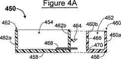
図4Aは、2つの別々のチャンバ452(たとえば、412bと比較されたい)および454(たとえば、414と比較されたい)を有するカプセル詰めパッケージアセンブリ450(たとえば、400と比較されたい)を示している。各チャンバ452および454は、それぞれ、ベース部456および458を有している(たとえば、406と比較されたい)。この説明では、ベース部456および458は正方形である。
【0098】
チャンバ452は、そのベース部456の周囲から(図に示されているように)上向きに延びている側壁460を有している。「スライス」型の断面図であるこの図には、側壁の4つの部分のうちの2つが示されており、460aおよび460bが付されている。図から明白であるように、2つのチャンバ452および454が互いに結合されるとき、側壁部460aは「外側」側壁部の機能を果たし、側壁部460aは「内側」側壁部の機能を果たす。
【0099】
同様に、チャンバ454は、そのベース部458の周囲から(図に示されているように)上向きに延びている側壁462を有している。この図には、側壁の4つの部分のうちの2つが示されており、462aおよび462bが付されている。図から明白であるように、2つのチャンバ462および464が互いに結合されるとき、側壁部462aは「外側」側壁部の機能を果たし、側壁部462aは「内側」側壁部の機能を果たす。
【0100】
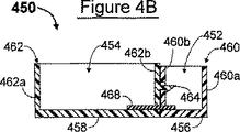
図4Aは、チャンバ454の内側側壁部462bからチャンバ452の方向に(図では左に向かって)突き出る複数の細長い部材464であってよく、遠位端にかえしまたは歯止めが形成されるように示されているものの代表的な例を示している。細長い部材464は、チャンバ454と一体に形成する(たとえば、チャンバ454と共に成形する)ことが好ましい。開口部(穴)466が、チャンバ452の内側側壁部460bの、細長い部材464の位置に対応する位置に形成されている。このように、2つのチャンバ452および454が互いに結合されると、図4Bに示されているように、細長い部材464が開口部466を通って突き出て、それによって、チャンバ452の内側側壁460bがチャンバ454の内側側壁462bに密接して(当接して)配設された状態で、2つのチャンバ452および454が互いにしっかりと固定される。チャンバ452とチャンバ454が互いに結合されたとき、それらのベース部456および458の外面が、それぞれ、互いに同一平面になることが好ましい。
【0101】
図4Aはまた、チャンバ454内に成形された複数のリードフレームフィンガ468であってよく、かつ前述のように、チャンバ454の外側側壁462bを通って延びているものの代表的な例を示している。開口部(穴)470が、チャンバ452の内側側壁部460bの、リードフレームフィンガ468の位置に対応する位置に形成されている。このように、2つのチャンバ452および454が互いに接合されると、図4Bに示されているように、リードフレームフィンガ468が開口部470を通って突き出てチャンバ452内に入る。
【0102】
図4Aおよび図4Bの図は、図を明確にするために、カプセル詰めパッケージのチャンバ内のモジュールや部品が省略されていることが理解されなければならない。上記で図3に関して説明したように、チャンバ454がチャンバ452よりも高い側壁を有するように示されていることが認識されよう。
【0103】
前述のように2つのチャンバ452および454を互いに結合した後、2つのチャンバには個別にポッティング化合物(不図示)が充填される。チャンバ454が少なくとも開口部(466)の高さまで充填された場合、ポッティング化合物が細長い部材464の遠位端をチャンバ454内の所定の位置にしっかりと固定し、それによって、2つのチャンバが互いに分離されるのを防止するように働くことは明白である。
【0104】
2つのチャンバを互いに組み立てる前に、チャンバ452および454の側壁460aおよび462bの一方または両方の上に接着剤(不図示)を配置しておくことは、本発明の範囲内である。
【0105】
細長い部材464は、チャンバ454と一体に形成されているように示されている。これは一般に、2つのチャンバ452および454が互いに組み立てられた後、チャンバ452にカプセル詰め材料(後述)が充填される前にチャンバ454にカプセル詰め材料が充填される場合に好ましい。しかし、細長い部材464がチャンバ452の側壁460bと一体に形成され、開口部466がチャンバ464の側壁462bに形成されることは、本発明の範囲内である。
【0106】
外側チャンバへの部品の追加
前述のように、回路モジュール(102,202,302,402)はRFトランスポンダであってもよい。このような装置は通常、外部の読取機と通信する、以下に例を詳しく説明するアンテナを必要とする。
【0107】
図5Aおよび図5Bは、本発明のカプセル詰めパッケージアセンブリ500の応用例の一実施形態の平面図および側面図をそれぞれ示している。この応用例では、上記で図1Aおよび図1Bのカプセル詰めパッケージアセンブリ100に関して説明した種類のカプセル詰めパッケージ504について説明する。この実施形態では、追加の部品550が、カプセル詰めパッケージ504(104と比較されたい)の外側チャンバ512(112と比較されたい)内に配設されている。
【0108】
前述の実施形態(100)と同様に、この実施形態500において、カプセル詰めパッケージ504は、内面506a(106aと比較されたい)および外面506b(106bと比較されたい)を有する概ね平面状のベース部506(106と比較されたい)を有するのが適切である。外側側壁508(108と比較されたい)が、ベース部506の内面506aの周囲から(図5Bに最もよく示されているように)上向きに延びている。内側側壁510(110と比較されたい)が、ベース部506の内面506aの、ベース部506の周囲内にある位置から(図5Bに最もよく示されているように)上向きに延びている。このように、以下に詳しく説明するように、ポッティング化合物または2つの異なるポッティング化合物を別々に充填することのできる外側チャンバ512(112と比較されたい)および内側チャンバ514(114と比較されたい)の2つのチャンバが形成されている。
【0109】
前述の実施形態と同様に、回路モジュール502(102と比較されたい)は、カプセル詰めパッケージ504の内側チャンバ514内に配設され、適切な接着剤518(118と比較されたい)を用いて(図5Bに最もよく示されているように)ベース部506の内面506aに取り付けられている。
【0110】
前述の実施形態と同様に、回路モジュール502は、電子部品522(122と比較されたい)および他の電子部品528(128と比較されたい)が前面上に配設されたPCB相互接続基板520(120と比較されたい)を有しており、電子部品522は、内側チャンバ514にポッティング化合物が充填されたときにセンサが覆われるのを防止するためのダム524(124と比較されたい)に囲まれた圧力センサであってもよい。
【0111】
前述の実施形態と同様に、PCB520のパッド526(126と比較されたい)は、内側チャンバ514内から内側側壁510を通って外側チャンバ512内へ延びる複数の細長いリードフレーム「フィンガ」530a..530h(130a..130hと比較されたい)の内端部にボンドワイヤ532(132と比較されたい)を用いて接続されている。
【0112】
前述の実施形態と同様に、回路モジュール502はRFトランスポンダであってもよく、電子部品522は圧力センサ部品であってもよく、電子部品528は集積回路であってもよく、カプセル詰めパッケージ504は空気入りタイヤ内に取り付けられていてもよい。
【0113】
外側チャンバ512内に配設される追加の部品550は、コイルアンテナ、言い換えると、2つの自由端552および554を有し、いくつかの巻き、およびいくつかの層を任意に有するコイルとして巻かれた、ある長さの絶縁(たとえば、エナメル被覆された)線で形成されたアンテナであるのが適切である。図5Aに最もよく示されているように、アンテナ線550の2つの自由端552および554は、それぞれ、2つのリードフレームフィンガ530eおよび530fの、外側チャンバ512内に露出された部分に接続されているように示されている。これらは単なるはんだ接続であってもよい。あるいは(不図示)、リードフレームフィンガ530eおよび530fの露出された部分は、それぞれ、アンテナ線の自由端552および554を機械的に「捕捉する」ノッチなどを備えることができる。
【0114】
外部部品との接続
前述の実施形態500では、カプセル詰めパッケージ504の外側チャンバ512内に配設されたアンテナ550を有するRFトランスポンダである電子装置について説明した。パッケージの外部の部品については説明していない。
【0115】
図6A,図6B,および図6Cは、RFトランスポンダである電子装置が、カプセル詰めパッケージの外部にあるアンテナ部品650(550と比較されたい)を有する応用例を示している。
【0116】
前述の実施形態(500)と同様に、この実施形態600において、カプセル詰めパッケージ604は、内面606a(506aと比較されたい)および外面606b(506bと比較されたい)を有する概ね平面状のベース部606(506と比較されたい)を有するのが適切である。外側側壁608(508と比較されたい)が、ベース部606の内面606aの周囲から(図6Bに最もよく示されているように)上向きに延びている。内側側壁610(110と比較されたい)が、ベース部606の内面606aの、ベース部606の周囲内にある位置から(図6Bに最もよく示されているように)上向きに延びている。このように、以下に詳しく説明するように、ポッティング化合物または2つの異なるポッティング化合物を別々に充填することのできる外側チャンバ612(512と比較されたい)および内側チャンバ614(514と比較されたい)の2つのチャンバが形成されている。
【0117】
前述の実施形態と同様に、回路モジュール602(502と比較されたい)は、カプセル詰めパッケージ604の内側チャンバ614内に配設され、適切な接着剤618(518と比較されたい)を用いて(図6Bに最もよく示されているように)ベース部606の内面606aに取り付けられている。
【0118】
前述の実施形態と同様に、回路モジュール602は、電子部品622(522と比較されたい)および他の電子部品628(528と比較されたい)が前面上に配設されたPCB相互接続基板620(520と比較されたい)を有しており、電子部品622は、内側チャンバ614にポッティング化合物が充填されたときにセンサが覆われるのを防止するためのダム624(524と比較されたい)に囲まれた圧力センサであってもよい。
【0119】
前述の実施形態と同様に、PCB620のパッド626(526と比較されたい)は、内側チャンバ614内から内側側壁610を通って外側チャンバ612内へ延びる複数の細長いリードフレーム「フィンガ」630a..630h(530a..530hと比較されたい)の内端部にボンドワイヤ632(532と比較されたい)を用いて接続されている。
【0120】
さらに、図6Aに最もよく示されているように、2つの別々のパッド(端子)630iおよび630jが示されている。これらのパッド630iおよび630jはリードフレーム全体のうちの一部として形成するのが適切である。これらのパッド630iおよび630jの機能について以下に詳しく論じる。
【0121】
前述の実施形態と同様に、回路モジュール602はRFトランスポンダであってもよく、電子部品622は圧力センサ部品であってもよく、電子部品628は集積回路であってもよく、カプセル詰めパッケージ604は空気入りタイヤ内に取り付けられていてもよい。
【0122】
アンテナ部品650は、パッケージ604の外部にあり、2つの自由端652および654を有する、ある長さのワイヤとして形成されている。あるいは、アンテナ部品650は、別々な長さを持つ2本のワイヤ(652および654)を有するダイポール型アンテナであってもよい。
【0123】
図6Cに最もよく示されているように、外部アンテナ部品650の自由端652および654は、パッケージ604の外側側壁608の開口部656および658をそれぞれ通過し、これにより、パッケージ604の外側チャンバ612内の端子630iおよび630jにそれぞれ取り付けられることができる。
【0124】
外側チャンバ612内に追加の部品660が任意に配設され、この部品660は、それぞれ2つのリードフレームフィンガ630eおよび630fに取り付けられた(例えば、はんだ付けされた)2本の一次リード線662および664を有し、かつ、それぞれ2つの追加の端子630iおよび630jに取り付けられた(例えば、はんだ付けされた)2本の二次リード線666および668を有するインピーダンス整合トランスフォーマであるのが適切である。
【0125】
前述の実施形態(500)と同様に、あるリードフレームフィンガ(たとえば、630eおよび630f)および追加の端子(630iおよび630j)は、それらに取り付けられる様々なワイヤを機械的に「捕捉する」ノッチなどを備えることができる。
【0126】
2段階のポッティングプロセス
前述のように、本発明のカプセル詰めパッケージアセンブリ(100,200,300,400,500,600)は、各チャンバにポッティング化合物または2つの異なるポッティング化合物を充填することのできる、2つ(または3つ以上)の異なるチャンバを有している。
【0127】
図7A〜図7Dは、カプセル詰めパッケージアセンブリ700(100と比較されたい)のチャンバ712(112と比較されたい)および714(114と比較されたい)にポッティング化合物を充填する技法700を示している。
【0128】
図7Aは、内面(フロア)706a(106aと比較されたい)および外面706b(106bと比較されたい)を有する概ね平面状のベース部706(106と比較されたい)を有する例示的なカプセル詰めパッケージ704(104と比較されたい)を示している。外側側壁708(108と比較されたい)が、ベース部706の内面706aの周囲から上向きに延びている。内側側壁710(110と比較されたい)が、ベース部706の内面706aの、ベース部706の周囲内にある位置から上向きに延びている。このように、内側チャンバ714(114と比較されたい)が外側チャンバ712(112と比較されたい)内に形成されている。
【0129】
回路モジュール702(102と比較されたい)は、ダム構造724(124と比較されたい)に囲まれた部品722(点線で示されている。122と比較されたい)と、PCBの表面上に取り付けられた他の部品728(128を参照されたい)とを有するPCB720(120と比較されたい)を有している。回路モジュール702は、適切な接着剤718(118と比較されたい)を用いて、ベース部706の内面706a上に配置されている。
【0130】
リードフレームもベース部706の内面706a上に配設されており、リードフレームは、内側チャンバ714から内側側壁710を通って外側チャンバ712内へ延びるリードフレームフィンガ730b(130bと比較されたい)および730f(130fと比較されたい)を有している。この図(図1Bと比較されたい)には、複数のリードフレームフィンガのうちの、この2つのみが示されている。選択されたパッド726が、前述のように、ボンドワイヤ732(132と比較されたい)を用いて、選択されたリードフレームフィンガに接続されている。
【0131】
図7Bに示されているように、カプセル詰めパッケージ704内に配設された電子部品をカプセル詰めする第1のステップでは、リードフレームフィンガ(730bおよび730f)の、内側チャンバ714内の部分、プリント配線板720、ワイヤ726を完全に覆い、さらに任意で部品728を完全に覆うのに十分であるが、内側チャンバ714を外側チャンバ712から分離する内側側壁710を超えて「あふれる」ほど多くはない量のポッティング化合物(カプセル詰め材料)715を、少なくとも部分的に内側チャンバ714に充填する。この図では、ポッティング材料715は、(中央部が上向きに湾曲し縁部が下向きに湾曲する)「正」メニスカスを有するように示されている。(中央部が下向きに湾曲し縁部が上向きに湾曲する)「負」メニスカスを有するポッティング化合物を使用して内側キャビティ714内に回路モジュール702をカプセル詰めできることは、本発明の範囲内である。任意に、内側キャビティ714にポッティング化合物を充填する前または後に、ダム構造124にシリコンゲル725を充填してもよい。
【0132】
ポッティング化合物715が硬化するにつれて、ポッティング化合物は収縮し、ポッティング化合物自体によってカプセル詰めされることはないが、カプセル詰め材料が収縮する際の応力を受ける他の部品(すなわち、PCB720)に取り付けられた部品722を含むカプセル詰め部品に物理的な応力を加えることができる。収縮によって生成される力は小さいが、圧力センサなどの応力検知部品(722)の性能に悪影響を及ぼす(あるいは、少なくとも応答をスキューまたはオフセットさせる)可能性がある。ポッティング化合物715が十分な時間にわたって硬化されると、ポッティング化合物715によってカプセル詰めされる部品に対してポッティング化合物715によって加えられるあらゆる応力が一様になり(すなわち、一定になり)、内側チャンバ714内の圧力検知部品に対して一定の作用を示す。
【0133】
図7Cに示されている次のステップでは、回路モジュール702の部品を以下のように電気的に試験作動(たとえば、較正)させることができる。例えば「ポゴ」ピン742および744をそれぞれ用いて、外部機器(不図示)から選択されたリードフレームフィンガ730xおよび730y(これらは図7Aに示されているフィンガ730bおよび730fではないので、この図ではこのように示されている)まで一時的に電気的に接続することができる。このようにして、回路モジュール702に電力を投入することができ、カプセル詰め回路モジュール702の部品を試験作動(たとえば、較正)させることができる。図示されていないが、カプセル詰め回路モジュールに電力を投入してモジュールを試験作動させる前または後に、外側チャンバ712内に追加の部品(たとえば、アンテナ550を参照されたい)を取り付け(リードフレームフィンガを介して)回路モジュール702に接続することができることが理解されなければならない。
【0134】
図7Dに示されている最終カプセル詰めステップでは、リードフレームフィンガ(730bおよび730f)の、内側チャンバ714内の部分、プリント配線板720、ワイヤ726を完全に覆い、さらに任意で、外側チャンバ712内に取り付けられた部品750(550と比較されたい)を完全に覆うのに十分であるが、内側チャンバ714を外側チャンバ712から分離する内側側壁710を超えて「あふれる」ほど多くはない量のポッティング化合物(カプセル詰め材料)713を、少なくとも部分的に内側チャンバ712に充填する。この図では、ポッティング材料713は、「正」メニスカスを有するように示されているが、「負」メニスカスを有していてもよい。
【0135】
ポッティング化合物713および715は、互いに同じ化合物であっても、あるいは異なる化合物であってもよい。
【0136】
カプセル詰めパッケージアセンブリの他の実施形態
図8Aおよび図8Bは、本発明のカプセル詰めパッケージアセンブリ800のさらに他の実施形態を示しており、この実施形態は、カプセル詰めパッケージ804(404と比較されたい)が、内側チャンバ(たとえば、114,214,314)を囲む外側チャンバ(たとえば、112,212,312)ではなく、並置された2つのチャンバ812および814(412aまたは412b、および414とそれぞれ比較されたい)を有するという点で、図4に関して記載されたカプセル詰めパッケージアセンブリ400に類似している。カプセル詰めパッケージアセンブリ800は、図を明確にするために、カプセル詰め材料を省略して示されており、2つのチャンバ812および814に前述のようにポッティング化合物を充填できることを理解されたい。
【0137】
カプセル詰めパッケージ804は、概ね平面状のベース部806(406と比較されたい)を有するという点で、前述のカプセル詰めパッケージに類似している。ベース部806は、内面806aおよび外面806bを有している。外側側壁808(408と比較されたい)が、ベース部806の周囲から上向きに延びている。内側側壁810がベース部806から上向きに延びており、2つのチャンバ812および814を形成すると共にこれらのチャンバを互いに分離している。第1のチャンバ812は幅寸法「x1」および長さ寸法「Y」を有している。第2のチャンバ814は幅寸法「x2」および長さ寸法「Y」を有している。
【0138】
第1の回路モジュール802(402と比較されたい)が、第1のチャンバ814内に配設されており、プリント配線板(PCB)820(120と比較されたい)に取り付けられた2つの電子部品828aおよび828bを有するように示されている。
【0139】
第2の回路モジュール803(802と比較されたい)が、第2のチャンバ812内に配設されており、プリント配線板(PCB)821(820と比較されたい)に取り付けられた2つの電子部品822および828cを有するように示されている。
【0140】
リードフレームフィンガの第1の部分830a..830dは、第2のチャンバ814内から外側側壁808を通ってカプセル詰めパッケージ804の外部まで延びており、リードフレームフィンガの第2の部分830e..830hは、第2のチャンバ814内から内側側壁810を通って第1のチャンバ812内に延びている。
【0141】
前述の実施形態と同様に、第1のPCB相互接続基板820を有する第1の回路モジュール802が第1のチャンバ814内に取り付けられており、PCB相互接続基板820は、その前面上に取り付けられた電子部品828aおよび828bを有していてもよい。PCB820上の導電パッド826(426と比較されたい)は、複数の細長いリードフレーム「フィンガ」830a..830h(430a..430hと比較されたい)の内側端部に、ボンドワイヤ832(432と比較されたい)を用いて接続されている。
【0142】
この実施形態では、第2のPCB相互接続基板821を有する第2の回路モジュール803が第2のチャンバ812内に取り付けられており、PCB相互接続基板821は、その前面上に取り付けられた1つまたは2つ以上の電子部品824および828cを有していてもよい。PCB821上の導電パッド827(826と比較されたい)は、複数の細長いリードフレーム「フィンガ」830e..830hの内側端部に、ボンドワイヤ833(832と比較されたい)を用いて接続されている。
【0143】
前述の実施形態と同様に、回路モジュール802はRFトランスポンダであってもよく、電子部品822は圧力センサ部品であってもよく、電子部品828aおよび828bは集積回路であってもよく、カプセル詰めパッケージ804は空気入りタイヤ内に取り付けられていてもよい。
【0144】
前述の実施形態と同様に、この実施形態において、カプセル詰めパッケージ804は成形プロセスによって熱可塑性材料で形成するのが適切であり、ベース部806、外側側壁808、および内側側壁810はすべて同じ厚さを有していてもよい。カプセル詰めパッケージ804は、以下のように、前述のカプセル詰めパッケージ104,204,および304の寸法と同等な(概ね等しい)寸法を有することが可能である。
(a)内側側壁808および外側側壁810の高さは外側側壁108の高さ「H」または外側側壁208の高さ「H’」または外側側壁308の高さ「H”」に概ね等しい。
(b)第1のチャンバ814の寸法「x2」および「Y」は、内側チャンバ114の寸法「d」、または内側チャンバ214の内側寸法「b」および「w」、または内側チャンバ314の内側寸法「d”」に概ね等しい。
(c)第2のチャンバ812の寸法「x1」は、寸法「x2」の概ね2分の1である。
【0145】
前述の実施形態と同様に、カプセル詰めパッケージ804は、すぐ上に記載された寸法に限られないことが明確に理解されなければならない。カプセル詰めパッケージ804およびその各部は、前述のものより大きくても、あるいは小さくてもよい。
【0146】
前述の実施形態と同様に、外側側壁808および内側側壁810がそれぞれ同じ高さを有することは必須ではない。
【0147】
カプセル詰めパッケージアセンブリの他の実施形態
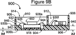
図9Aおよび図9Bは、本発明のカプセル詰めパッケージアセンブリ900のさらに他の実施形態を示しており、この実施形態は、カプセル詰めパッケージ904(804と比較されたい)が、並置された2つのチャンバ912および914(812および814と比較されたい)を有するという点で、前述のカプセル詰めパッケージアセンブリ800に類似している。カプセル詰めパッケージアセンブリ900は、図を明確にするために、カプセル詰め材料を省略して示されており、2つのチャンバ912および914に前述のようにポッティング化合物を充填できることを理解されたい。
【0148】
カプセル詰めパッケージ904は、概ね平面状のベース部906(806と比較されたい)を有するという点で、前述のカプセル詰めパッケージに類似している。ベース部906は、内面906aおよび外面906bを有している。図9Bに最もよく示され、以下に詳しく説明するように、ベース部906は、チャンバ914の部分よりもチャンバ912の部分の方が厚い。
【0149】
外側側壁908(808と比較されたい)が、ベース部906の周囲から上向きに延びている。内側側壁910(810と比較されたい)が、ベース部906から上向きに延びており、2つのチャンバ912および914を形成すると共にこれらのチャンバを互いに分離している。第1のチャンバ912は幅寸法「x1」および長さ寸法「Y」を有している。第2のチャンバ914は幅寸法「x2」および長さ寸法「Y」を有している。これらの寸法は、カプセル詰めパッケージアセンブリ800の前述の実施形態に関して記載された寸法に類似しているのが適切である。
【0150】
第1の回路モジュール902(802と比較されたい)が、第1のチャンバ914内に配設されており、プリント配線板(PCB)920(820と比較されたい)に取り付けられた2つの電子部品928aおよび928b(828aおよび828bと比較されたい)を有するように示されている。
【0151】
リードフレームフィンガの第1の部分930a..930dは、第2のチャンバ914内から外側側壁908を通ってカプセル詰めパッケージ904の外部まで延びており、リードフレームフィンガの第2の部分930e..930hは、第2のチャンバ914内から内側側壁910を通って第1のチャンバ912内に延びている。
【0152】
前述の実施形態と同様に、第1のPCB相互接続基板920を有する第1の回路モジュール902が第1のチャンバ914内に取り付けられており、PCB相互接続基板920は、その前面上に取り付けられた電子部品928aおよび928bを有していてもよい。PCB920上の導電パッド926(826と比較されたい)は、複数の細長いリードフレーム「フィンガ」930a..930fの内側端部にボンドワイヤ932(832と比較されたい)を用いて接続されている。
【0153】
この実施形態では、電子部品922(回路モジュール803と比較されたい)が第2のチャンバ912内に配設されて(取り付けられて)いる。電子部品922上の導電パッド927(827と比較されたい)は、複数の細長いリードフレーム「フィンガ」930e..930fの内側端部にボンドワイヤ933(833と比較されたい)を用いて接続されている。
【0154】
前述の実施形態と同様に、回路モジュール902はRFトランスポンダであってもよく、電子部品922は圧力センサ部品であってもよく、電子部品928aおよび928bは集積回路であってもよく、カプセル詰めパッケージ904は空気入りタイヤ内に取り付けられていてもよい。
【0155】
前述の実施形態と同様に、この実施形態において、カプセル詰めパッケージ904は成形プロセスによって熱可塑性材料で形成するのが適切であり、カプセル詰めパッケージ904は大部分が前述のカプセル詰めパッケージの寸法と同等な(概ね等しい)寸法を有していてもよい。
【0156】
たとえば、内側側壁908および外側側壁910の高さは、外側側壁108の高さ「H」または外側側壁208の高さ「H’」または外側側壁308の高さ「H”」に概ね等しくてもよい。しかしながら、図9Bに最もよく示されているように、内側側壁910と、外側側壁908の、内側側壁910と共にチャンバ912に結合された部分908a,908b,および908cとは、外側側壁908の残りの部分908d,908e,および908fよりも高いことが好ましい。
【0157】
第1のチャンバ914の寸法「x2」および「Y」は、内側チャンバ114の寸法「d」、または内側チャンバ214の内側寸法「b」および「w」、または内側チャンバ314の内側寸法「d”」に概ね等しく、たとえば約5.1mmであってもよい。
【0158】
第2のチャンバ912の寸法「x1」は寸法「x2」の概ね2分の1であり、たとえば約10.6mmであってもよい。寸法「X」(X=x1+x2)は約15.7mmであるのが適切である。
【0159】
前述の実施形態と同様に、カプセル詰めパッケージ904は、すぐ上に記載された寸法に限られないことが明確に理解されなければならない。カプセル詰めパッケージ904およびその各部は、前述のものより大きくても、あるいは小さくてもよい。
【0160】
前述のように、ベース部906は、チャンバ914の部分よりもチャンバ912の部分の方が厚い。より詳しくは、図9Bに最もよく示されているように、ベース部906の外面906bは、前述の実施形態と同様に概ね平面状である。
【0161】
この実施形態では、電子部品922が取り付けられたチャンバ912内のベース部の内面940は、ベース部906の外面906bより距離「h3」だけ上に位置している。チャンバ914内のベース部の内面は、電子モジュール902が取り付けられる領域でありベース部906の外面906bより距離「h4」だけ上に位置している中央領域942を有している。距離「h3」は距離「h4」よりも大きい(h3>h4)。
【0162】
チャンバ914内のベース部の内面は階段状になっており、したがって、中央領域942の外側の領域944はベース部906の外面906bより距離「h3」だけ上に位置している。このように、内側側壁910を通って延びるリードフレームフィンガ(たとえば、930f)は、チャンバ914の内面部944およびチャンバ912の内面940上の平面に位置している。同様に、中央領域942の外側に位置する、チャンバ内のベース部の内面の他の部分も、ベース部906の外面906bより距離「h3」だけ上に位置するように階段状にすることができる。この例では、チャンバ914内のベース部の内面の部分946は、ベース部906の外面906bより距離「h3」だけ上に位置するように階段状になっている。このように、すべてのリードフレームフィンガを互いに同一平面に配置することができる。
【0163】
図9Bに最もよく示されているように、これは、電子部品922が電子モジュール902よりも高い位置に配設されることをもたらす。重要な点として、チャンバ912内のベース部の厚さを厚くすると、その上に取り付けられる電子部品922のための全体的により剛性の高いベースが形成される。電子部品922が、前述のような圧力センサである場合、圧力センサを比較的剛性のベースに取り付けることが有益であることは明白である。
【0164】
図9Aおよび図9Bはまた、一部のリードフレーム、この場合はリードフレームフィンガ930a..930dがパッケージの外部まで延びることができ、それによってリードフレームを金型内に支持できるという、上記に簡単に説明した概念を示している。この例では、パッケージの外部まで延びない他のリードフレームフィンガ930eおよび930fを、その下に位置する絶縁膜(不図示)、またはリードフレーム自体の一部を形成し、後でリードフレームから削り取ることのできる金属製ウェブまたはブリッジ(やはり不図示)によって、リードフレームフィンガ930a..930dと共に支持することができる。本発明の当業者には、リードフレームを金型内に支持する必要があることと、そのために使用できる多数の方法とが容易に理解されよう。このための技法は応用例ごとに異なるので、本発明の説明においてそのような技法についてさらに詳しく説明する必要はない。
【0165】
カプセル詰めパッケージアセンブリの更なるパッケージング
図9Cおよび図9Dは、本発明の例示的なカプセル詰めパッケージアセンブリ900をさらにパッケージングする技法を示している。カプセル詰めパッケージアセンブリ900は、図を明確にするために、カプセル詰め材料を省略して示されており、アセンブリの2つのチャンバ(912および914)に前述のようにポッティング化合物を充填できることを理解されたい。
【0166】
追加のカプセル詰めパッケージ954は、概ね平面状のベース部956を有する簡素なコップ状構造の形をしている。ベース部956は、直径「P」を有する円形であり、内面956aおよび外面956bを有するのが適切である。高さ「Q」を有する環状側壁958が、ベース部956の周囲から上向きに延びている。このように、筒状チャンバ960が形成されている。側壁の高さ「Q」は、カプセル詰めパッケージ904の側壁の高さと等しいか、あるいはそれよりも高いか、あるいは(好ましくは)それよりも低い。
【0167】
図示されているように、カプセル詰めパッケージ(904)のベース部(906)の外面(906b)が追加のカプセル詰めパッケージ954のベース部956の内面に接触して配設された状態で、カプセル詰めパッケージアセンブリ900全体がチャンバ912内に配設されている。シアノアクリレート(「スーパーグルー」)などの適切な接着剤962を使用して、カプセル詰めパッケージアセンブリ900を追加のカプセル詰めパッケージ954に接合することができる。
【0168】
追加のカプセル詰めパッケージ954の適切な寸法は以下のとおりである。
・ベース部956bの直径「P」は25.0mmから60.0mmの範囲であり、たとえば約32.0mmである。
・側壁958の高さ「Q」は0.3mmから8.0mmの範囲であり、たとえば約4.0mmである。
・側壁958の厚さ「t」は0.3mmから2.0mmの範囲であり、たとえば約1.0mmである。
【0169】
前述の実施形態と同様に、追加のカプセル詰めパッケージ954は、すぐ上に記載された寸法に限られないことが明確に理解されなければならない。カプセル詰めパッケージアセンブリ900が追加のカプセル詰めパッケージ954内に収まる限り、追加のカプセル詰めパッケージ954およびその各部は、前述のものより大きくても、あるいは小さくてもよい。追加のカプセル詰めパッケージ954は、前述のカプセル詰めパッケージ(たとえば、104)と同じ材料で成形するのが適切である。
【0170】
カプセル詰めパッケージアセンブリの例示的な使用法
図10Aおよび図10Bは、本発明のカプセル詰めパッケージアセンブリの様々な実施形態の例示的な使用法を示している。前述のように、本発明のカプセル詰めパッケージアセンブリの例示的な用途は、電子部品(たとえば、122)が圧力センサ部品であり、カプセル詰めパッケージ(たとえば、104)が、外部の読取機/呼掛け応答機またはタイヤの上に乗っている車両の運転手にタイヤの圧力情報を与えるために空気入りタイヤ内に取り付けられる場合に、RFトランスポンダである回路モジュール(たとえば、102)を収容することである。
【0171】
図10Aは、前述の実施形態のカプセル詰めパッケージアセンブリ(カプセル詰めされた他のパッケージ954を含め、100,200,300,400,450,500,600,700,800,または900)のうちのいずれであってもよい、カプセル詰めパッケージアセンブリ1000を示している。パッケージアセンブリ1000は、シート同士の間から気泡を除去するように押し付けられかつ縁部の周りで密封された、ゴムシートのような2枚の薄いシート1002および1004の間に「挟まれる」ように示されている。接着剤1006が、シート1002の(図における)上面上に配置されている。このように、「サンドイッチ」パッチ1010内のカプセル詰めされたトランスポンダ装置は、空気入りタイヤの内面に取り付けることができるようになっている。トランスポンダ装置を「サンドイッチ」パッチ内に配設する方法は公知であり、本質的に本発明の一部を構成しない。
【0172】
図10Bは、空気入りタイヤ1012内の内面上に取り付けられた図10Aのサンドイッチパッチ1010を示している。アンテナ1024を有するワンド1022を持つ外部の読取機/呼掛け応答機を使用して、空気入りタイヤ1012内に配設されたトランスポンダ回路をポーリングし(回路に呼び掛けし)、トランスポンダ回路から検索されたデータを液晶ディスプレイ(LCD)パネルなどの適切なリードアウト1026上に表示するのが適切である。外部機器を使用してトランスポンダ装置と対話することは公知であり、本質的に本発明の一部を構成しない。
【0173】
本発明をその実施形態と組み合わせて説明したが、上記の説明を考慮して当業者に多数の代替形態、修正形態、および変形形態が明らかになることは明白である。したがって、添付の請求の範囲の趣旨および範囲内のそのようなすべての代替形態、修正形態、および変形形態を包含することが意図されている。
【0174】
たとえば、前述の様々な実施形態に記載された様々な特徴のうちの選択された特徴を「組み合わせかつ整合させ」て、このような特徴を組み込んださらに他の実施形態を生み出すことができる。たとえば、図3の実施形態のカプセル詰めパッケージング(304)のより高い内側側壁(310)の特徴は、図5の実施形態のカプセル詰めパッケージ504の追加の部品(550)の特徴と組み合わせることができる。
【図面の簡単な説明】
【図1A】 本発明の封止パッケージアセンブリの実施形態の平面図である。
【図1B】 本発明による、図1Aの封止パッケージアセンブリの、図1Aの1B−1B線で切断した側断面図である。
【図2A】 本発明の封止パッケージアセンブリの代替実施形態の平面図である。
【図2B】 本発明の図2Aに示されている封止パッケージアセンブリの代替実施形態の側断面図である。
【図3】 本発明の封止パッケージアセンブリの代替実施形態の側断面図である。
【図4】 本発明の封止パッケージアセンブリの代替実施形態の平面図である。
【図4A】 本発明の封止パッケージアセンブリの代替実施形態の分解側断面図である。
【図4B】 本発明による、図4Aの封止パッケージアセンブリの代替実施形態の組立て後の側断面図である。
【図5A】 パッケージの外側チャンバ内に追加の電子部品が配設された、図1Aに示されている実施形態に類似している、本発明の封止パッケージングアセンブリの実施形態の平面図である。
【図5B】 本発明による、図5Aの封止パッケージアセンブリの、図5Aの5B−5B線で切断した側断面図である。
【図6A】 追加の電子部品がパッケージの外部に配設され、かつパッケージ内にある回路モジュールに接続されている、図5Aに示されている実施形態に類似している、本発明の封止パッケージアセンブリの実施形態の平面図である。
【図6B】 本発明による、図6Aの封止パッケージアセンブリの、図6Aの6B−6B線で切断した側断面図である。
【図6C】 本発明による、図6Aの封止パッケージアセンブリの、図6Aの6C−6C線で切断した側断面図である。
【図7A】 本発明の封止パッケージアセンブリのチャンバにポッティング化合物を充填する技法を示す断面図である。
【図7B】 本発明の封止パッケージアセンブリのチャンバにポッティング化合物を充填する技法を示す断面図である。
【図7C】 本発明の封止パッケージアセンブリのチャンバにポッティング化合物を充填する技法を示す断面図である。
【図7D】 本発明の封止パッケージアセンブリのチャンバにポッティング化合物を充填する技法を示す断面図である。
【図8A】 本発明の封止パッケージアセンブリの代替実施形態の平面図である。
【図8B】 本発明による、図8Aの封止パッケージアセンブリの、図8Aの8B−8B線で切断した側断面図である。
【図9A】 本発明の封止パッケージアセンブリの代替実施形態の平面図である。
【図9B】 本発明による、図9Aの封止パッケージアセンブリの、図9Aの9B−9B線で切断した側断面図である。
【図9C】 本発明の封止パッケージアセンブリをさらにパッケージングする技法を示す平面図である。
【図9D】 本発明による、図9Cの封止パッケージアセンブリの、図9Cの9D−9D線で切断した側断面図である。
【図10A】 本発明の封止パッケージアセンブリを、空気入りタイヤなどの監視される物体に組み付けられるようにする技法を示す側断面図である。
【図10B】 本発明による、空気入りタイヤなどの監視される物体に組み付けられた、本発明の封止パッケージアセンブリの概略図である。[0001]
TECHNICAL FIELD OF THE INVENTION
The present invention relates to the interconnection and packaging of electronic components, and more particularly to circuit modules that include sensors and may be disposed in harsh environments.
[0002]
Background of the Invention
As used herein, the term “circuit module” refers to an interconnect substrate such as a printed wiring board (PCB) to which electronic components are attached. PCB is a multi-layer substrate in which insulating material layers and conductive material layers are alternately provided. The conductive material of the conductive layer is patterned to have conductive “lines” or “traces” that carry signals from one location on the PCB to another location on the PCB. In the case of multiple conductive layers, typically at least one of these layers is disposed on the surface of the PCB (eg, the “top” surface). The conductive layer on the top surface of the PCB has (i) a “pad” that serves as a terminal connected to an external device such as a socket, or (ii) a lead wire of an electronic component attached to the PCB. It may be patterned to have. Thus, electronic components attached to the PCB may connect to each other through pads on the top surface of the PCB and conductive traces on the PCB.
[0003]
Examples of electronic components that may be incorporated into circuit modules include:
(A) "active" electronic components such as integrated circuit (IC) devices, etc.
(B) "passive" electronic components such as resistors, capacitors, inductors (including transformers), etc.
(C) Switches, relays, etc.
(D) There are sensors, transducers, and the like.
[0004]
The electronic components incorporated in the circuit module are “packaged” or “bare” (not packaged).
[0005]
As an example of a “packaged electronic component”, a semiconductor memory device (for example, a dynamic random semiconductor device) attached to and electrically connected to a lead frame having a plurality of elongated conductive members “fingers” and coated with plastic. Access memory, or DRAM chip). The outer portion of the lead frame fingers extends outward (projects) from the molded plastic body and can be connected to conductive pads on the interconnect substrate (PCB). In this way, a plurality of DRAMs packaged in plastic can be attached and connected to the PCB, thereby forming a memory module. This memory module can be plugged into a socket mounted on another interconnect substrate such as a “motherboard” of a computer system, in which case the conductive pads disposed on one or both surfaces of the memory module are sockets It is in electrical contact with the elastic contact member inside.
[0006]
Examples of “bare electronics” are bonded to an interconnect substrate (using a “die attach” adhesive) and extend between a pad on a semiconductor device and a pad on the interconnect substrate There is a semiconductor device electrically connected to a thin wire. To protect electronic components and wires, it is known to apply a small amount of “glob top” epoxy or the like over the electronic components and thin wires.
[0007]
A known technique for providing such a connection to a semiconductor device is “wire bonding”. Typical wire bonding techniques are:
a. A fine (eg, 1 mil diameter) gold (or gold alloy) bond wire is fed through a capillary located above the terminals (pads) of the interconnect substrate or electronic components attached thereto,
b. Bond (eg, weld) the end of the bond wire to the terminal using a combination of pressure and heat or ultrasonic vibration;
c. Pull the capillary so that the bond wire is "drawn" from the capillary, thereby forming some slack in the bond wire,
d. Moving the interconnect substrate (or conversely the capillary), thereby placing the capillary above the other terminal (pad) on the electronic component or interconnect substrate;
e. Join the middle part of the bond wire to this other terminal,
f. Cutting the bond wire, thereby obtaining a “loop” of bond wires extending between terminals (pads) on the electronic component and terminals (pads) on the interconnect substrate.
[0008]
The present invention utilizes many of the techniques described above to create new techniques for packaging electronic circuit modules and components. Before proceeding with the description of the present invention, it is necessary to understand certain other relevant aspects of electronic packaging.
[0009]
Before shipping electronic components and circuit modules for installation (eg, integration into a system), test or more to ensure that the electronic components and circuit modules operate as designed In a broad sense, it is often necessary to operate on a trial basis. This includes calibrating or personalizing electronic components and circuit modules in the case of electronic components and circuit modules that can and need to be calibrated.
[0010]
Returning to the example of the DRAM device in which the plastic is coated and the outer portion of the lead frame finger protrudes from the molded plastic body, the “temporary” relationship between the lead frame finger and the portion protruding from the package body will be described. The DRAM device can be tested by making a “typical” electrical connection using pins, needles, and the like. As an example of a pin suitable for making a temporary electrical connection with a terminal of an electronic component (in this example, a protruding portion of a lead frame finger), generally an inner portion protruding from the outer portion and an inner portion are A so-called “pogo” pin is a pin that has a spring that keeps it pressed against the extended position. Alternatively, in the case of a memory module having a plurality of DRAM memory devices packaged in plastic attached and connected to a PCB, the module is inserted into a test socket of the test system, and the test socket is temporarily electrically connected to the PCB. The entire module can then be tested by “accessing” the components attached to the PCB through the PCB's conductive traces.
[0011]
Similarly, when projecting a packaged circuit module, the protruding terminals of the module are accessed in a broad sense. For example, a module may have non-volatile memory (NVM) components that can be programmed by supplying signals to the external terminals of the module. Alternatively, the module can be programmed with a personalized component such as, for example, a DIP switch that is part of the module and accessible from outside the module.
[0012]
On the other hand, in the final form, there is no terminal protruding from the outside of the circuit module, or the personalized parts cannot be accessed from the outside, and in some cases, the power supply connection (for example, the battery terminal) cannot be accessed. Consider the case of a circuit module. The question is how to test this module. Examples of such packaged circuit modules that lack the inherent ability to be tested and personalized in the final configuration include exposure to the ambient environment outside the packaged circuit module. With the exception of sensors (eg, temperature sensors), there are transponder modules that are completely sealed to insulate their electronic components from the surrounding environment.
[0013]
As will be apparent from the following description, the present invention provides an electronic module and component having at least two chambers (cavities).SealingIt is invention regarding the package to do.
EP-A-0 289 439 discloses a single chamber of a closed box, which is partially filled over a first circuit module, thereby defining a “first chamber”.SealingAnd the chamber,The remaining unfilled portion is left as the “second chamber”. The second circuit module is the top of the first fillingPartThe second chamber is then filled with a second filling covering the second circuit module. Appropriate internal connections between the circuit module and the external connector are made by conductors embedded in the first and second fillings, thereby providing communication between the chambers.
[0014]
US Pat. No. 5,239,126(Sony, 1993) discloses a high frequency circuit package comprising a conductive substrate and an upper shielding case and a lower shielding case forming an upper shielding chamber and a lower shielding chamber, respectively. High frequency circuits are attached to the upper and lower surfaces of the conductive substrate in the upper and lower chambers, respectively. This patent is incorporated herein by reference in its entirety and is cited as an example of an electronic package having two chambers.
A similar package with three shielded chambers discloses a structure for shielding electronic components from external electromagnetic fields.US Pat. No. 5,504,659It is described in. The outer housing holds a single printed circuit board that separates the “contaminated” space from the “clean” space and shields the components of the device itself. In FIG. 2, the contaminated space (24) forms one chamber and the housing forms a shielding partition wall, which is a clean space (28) forming a second chamber. ), And a pipe line connects the chambers through the shielding partition wall. The printed circuit board is also utilized to shield the two first chambers from the third clean space on the other side of the printed circuit board in the housing.
[0015]
US Pat. No. 5,627,406 (Pace, 1997), which is incorporated herein by reference in its entirety, discloses an electronic packaging module. The hybrid circuit (310) forms a base and has ridges (330) and metal pads (331) on its surface. Semiconductor device (340) and other components (341) are bonded to the ridges and pads. A metal or ceramic frame (350) having openings for semiconductor devices and other components is disposed on the surface of the base and is fitted around the semiconductor devices and other components. A plug (370) fitted inside the opening of the frame is in contact with the back of the semiconductor device, and is joined to the frame so as to seal the module. This packaging moduleSealingReference is made by way of example to a package that is not a module but has two (or more) juxtaposed cavities (ie, chambers) with electronic components disposed within each cavity.
[0016]
In some cases, the circuit module is intended to be placed in a “harsh” environment, and it is desirable to isolate the electronic components of the circuit module from the environment. An example of such an application of a circuit module is an RF transponder disposed in a vehicle pneumatic tire. See, for example, “Pneumatic Tires with Integrated Circuit Transponders and Pressure Transducers” described in commonly owned US Pat. No. 5,218,861, which is incorporated herein by reference in its entirety.
[0017]
Object of the invention
The object of the present invention is defined in one or more of the appended claims and, therefore, achieves one or more of the following sub-objects. An improved electronic module that can be configured and a method for packaging the improved electronic module.
[0018]
Accordingly, it is an object of the present invention to provide an improved method for packaging electronic circuit modules.
[0019]
Another object of the present invention is to provide an improved electronic module package.
[0020]
Another object of the present invention is to provide an electronic circuit module.Sealing(Potting) and then packaging so that it can be tested (eg, calibrated) and then providing a separate potting method for other electronic components disposed within the package. .
[0021]
Summary of the Invention
According to the present invention, an electronic component isSealingThe package to be provided has at least two chambers (cavities). These chambers include a chamber and electronic components and modules disposed in the chamber.SealingThe top is open so that the material (potting compound) can be at least partially filled. The chamber is suitably molded by an injection molding process from a plastic material such as thermosetting epoxy, polyphenylene sulfide, Ryton ™.
[0022]
According to one aspect of the invention, the lead frame is disposed in a package and has elongated conductive elements (lead frame fingers) that extend from one chamber into the other chamber. In this way, an electronic component or module disposed in one chamber can be interconnected with an electronic module or component disposed in the other chamber.
[0023]
According to one aspect of the invention, the chambers are separately (individually)SealingThe material can be filled. Thus, for example, an electronic module disposed in one chamber and connected to a portion of the lead frame in the cavity.SealingPotting with material and then making an electrical connection from an external device (eg, test equipment) to a portion of the leadframe finger that extends into the other chamber (eg, using “pogo pins”) Can be electrically tested (eg, calibrated or personalized). Therefore, the potted module in one chamber can be tested and operated with electronic components in the other chamber, or can be tested without electronic components in the other chamber. You can also. After test activation of the potted module, the other chamber and the electronic components disposed in the other chamber can be potted without “influencing” the already test activated and potted module.
[0024]
In an embodiment of the invention, the outer chamber of the two chambers surrounds the inner chamber. This embodiment includes one chamber surrounding the other chamber and the latter chamber further surrounding another chamber.
[0025]
In other embodiments of the invention, one chamber is adjacent to another chamber. This can be a total of two chambers, one on each side of the other chamber, a total of three chambers, one on each side of the triangular chamber, or a side of the rectangular chamber. Multiple chambers are adjacent to other chambers, including a total of four chambers one at a time.
[0026]
According to one aspect of the invention, the sidewall of one chamberButHigher than the other chamber. Thus, for chambers with higher side walls,SealingWhile minimizing the risk of material overflowing to nearby chambers, for exampleSealingThe material can be fully filled.
[0027]
According to one aspect of the present invention, a portion of the lead frame extends outside the package through the outer wall of the package.
[0028]
According to another aspect of the present invention, an opening for connecting to a component outside the package can be provided on the outer surface (outer wall) of the package.
[0029]
In a typical package application, the electronic modules and components contained (and potted) in the package have an RF transponder and a pressure sensor so that the entire package assembly can be mounted in a pneumatic tire. it can.
[0030]
Other objects, features and advantages of the present invention will become apparent from the following description.
[0031]
Brief Description of Drawings
Reference will now be made in detail to the preferred embodiments of the invention, examples of which are illustrated in the accompanying drawings. The drawings are exemplary and not limiting.
[0032]
For clarity of illustration, certain elements in selected drawings mayScaleIs not drawn.
[0033]
Similar elements throughout the drawings are often referred to by similar reference numerals. For example, element 199 in one figure (or embodiment) is similar in many respects to element 299 in another figure (or embodiment). Where there is such a relationship between similar elements in each different figure or embodiment, that relationship will become apparent throughout the specification, including the claims and abstract as appropriate.
[0034]
In some cases, similar elements may be referred to with similar reference numerals in a single drawing. For example, the plurality of elements 199 may be referred to as 199a, 199b, 199c, etc.
[0035]
The cross-sectional views shown herein are in the form of “slices” or “myopic” cross-sectional views, with certain background lines visible in the true cross-sectional view omitted for clarity. Yes.
[0036]
The structure, operation, and advantages of preferred embodiments of the present invention will become more apparent when the following description is considered in conjunction with the accompanying drawings.
[0037]
Detailed Description of the Invention
1A and 1B illustrate the present invention.SealingAn embodiment of a
[0038]
The encapsulating
[0039]
When the
[0040]
As best shown in FIG. 1A, the
[0041]
The encapsulating
(A) The diameter “D” of the base portion 106 (and the outer side wall 108) is25.0mmFrom50.0mmFor example,32.0mmIt is.
(B) The diameter “d” of the
(C) The heights “H” of the
(D) The thickness of the
[0042]
It should be clearly understood that the encapsulating
[0043]
It is not essential that the
[0044]
The capsule-packing
[0045]
It is not essential that the encapsulated
[0046]
In general, the encapsulating
[0047]
The
[0048]
The
[0049]
As best shown in FIG. 1A, an
[0050]
[0051]
1A and 1B show a plurality of (eight of which are shown) elongated leadframe “fingers” (conductive ribbon-like elements) disposed on the
[0052]
It is within the scope of the present invention for the lead frame to have any of a variety of conductor patterns as well as elongated “finger” shapes. It is preferable that there are no paths crossing each other among the conductive paths of the lead frame. If complex interconnections that require crossing are required, multilayer interconnect substrates can be used instead of leadframe components.
[0053]
As best shown in FIG. 1B, the lead frame is suitably molded directly in the encapsulated
[0054]
In this embodiment, and other embodiments described below (eg, shown in FIGS. 4A and 9A), a portion of the leadframe component (130) (eg, the leadframe finger) may be packaged (104). ) So that the lead frame can be held in place (clamped) while the mold (not shown) is clamped around the lead frame part to mold the It should be understood that it may extend through.
[0055]
As best shown in FIG. 1B, the
[0056]
In the exemplary application of the present invention,
[0057]
In certain applications, where the
[0058]
Even if the inventor constructs a prototype RF transponder as described above and shields the
[0059]
Accordingly, a primary object of the present invention is to provide a technique for partially encapsulating the
[0060]
Alternative embodiments
The encapsulating
[0061]
FIG. 2A illustrates an alternative embodiment of the encapsulated
[0062]
In general, as best shown in FIG. 2A, the main difference between the encapsulating
[0063]
As best shown in FIG. 2B, other differences between the encapsulating
[0064]
Similar to the previous embodiment, in this embodiment, the encapsulated
[0065]
The
[0066]
Similar to the previous embodiment, in this embodiment, the encapsulating
(A) The diameter “B” of the base portion 206 (and the outer side wall 208) is25.0mmFrom50.0mmFor example,32.0mmIt is.
(B) The diameter “b” of the
(C) The base width dimension “W” of the base portion 206 (and the outer side wall 208) is25.0mmFrom50.0mmFor example,32.0mmIt is.
(D) The width dimension “d” of the
(E) The heights “H” of the
(F) The thicknesses of the
[0067]
As with the previous embodiment, it should be clearly understood that the encapsulated
[0068]
Similar to the previous embodiment, it is not essential that the
[0069]
Similar to the previous embodiment, the capsule package of the present invention204It is not essential to form a thermoplastic material.
[0070]
In general, the encapsulating
[0071]
Similar to the previous embodiment, the
[0072]
Similar to the previous embodiment,
[0073]
Similar to the previous embodiment, the pads 226 (compare 126) of the
[0074]
Similar to the previous embodiment,
[0075]
Alternative embodiments
The above has described the encapsulated packages (104 and 204) having the same height (H, H ') inner side walls (110, 210) and outer side walls (108, 208). It is within the scope of the present invention that the inner and outer sidewalls of the encapsulated package can have different heights.
[0076]
FIG. 3 shows another encapsulation package assembly 300 (compare 100, 200) that includes a
[0077]
Similar to the previous embodiment (100, 200), a circuit module having a PCB interconnect substrate 320 (compare 120, 220) is used with a suitable adhesive 318 (compare 118, 218). It is attached to the
[0078]
Similar to the previous embodiment (100, 200), the circuit module 302 may be an RF transponder, the electronic component 322 may be a pressure sensor component, the
[0079]
Similar to the previous embodiment (100, 200), in this
(A) The height “H” of the
(B) The transverse dimension (eg, diameter) of the base portion 306 (and the outer sidewall 308) is approximately equal to the dimension “D” of the
(C) The transverse dimension (eg, diameter) of the
(D) the
[0080]
As with the previous embodiment, it should be clearly understood that the encapsulating
[0081]
Alternative embodiments
The above has described a capsule packaging (104, 204, 304) having two chambers, an outer chamber (112, 212, 312 respectively) surrounding an inner chamber (114, 214, 314, respectively). It is within the scope of the invention to have two (or more) chambers adjacent to each other.
[0082]
FIG. 4 illustrates yet another embodiment of the encapsulating
[0083]
This
[0084]
In this
[0085]
The encapsulating
[0086]
The first
[0087]
The second
[0088]
The first and second
[0089]
Thus, three chambers are compared, i.e., two outer chambers 412a and 412b (112, 212, 312), each containing electronic components or modules, each of which can be separately filled with potting compounds. ), And the inner chamber 414 (compare 114, 214, 314).
[0090]
Similar to the previous embodiment (100, 200, 300), the PCB interconnect substrate420The circuit module having (compare 120, 220, 320) is attached to the inner surface 406a of the base 406 using a suitable adhesive 418 (compare 118, 218, 318).
[0091]
If only one outer chamber is adjacent to the inner chamber (more precisely, this is adjacent to the “second” chamber since the two chambers in parallel have neither “inner” nor “outer” It is within the scope of the present invention that all lead frame fingers extend into the second chamber from within one chamber, through the side walls separating the two chambers in parallel. is there. Alternatively, some lead frame fingers can extend from within the first or second chamber to a position beyond the outer wall of the encapsulated package.
[0092]
Similar to the previous embodiment (100, 200, 300), the circuit module402May be an RF transponder, an electronic component422May be pressure sensor components, electronic components428May be an integrated circuit, encapsulated package404May be mounted in a pneumatic tire.
[0093]
Similar to the previous embodiment (100, 200, 300), in this
(A) The height of the inner and outer sidewalls is approximately equal to the height “H” of the
(B) The dimensions “x” and “y” of the inner chamber 414 are the dimensions “d” of the
(C) The dimension “x1” is not greater than approximately one quarter of the dimension “X”, the dimension “x2” is similarly not approximately greater than one quarter of the dimension “X”, and the dimension “x1” is It is approximately equal to the dimension “x2”.
[0094]
As with the previous embodiment, it should be clearly understood that the encapsulating
[0095]
Similar to the previous embodiment, it is not essential that the
[0096]
2 (or more) separate, connectable chambers
Described herein are several embodiments in which two or more chambers of an encapsulated package are formed as a single unit structure. It is within the scope of the present invention to form two (or more) chambers of the encapsulated package separately and then combine together to form a single encapsulated package.
[0097]
FIG. 4A shows a capsule package assembly 450 (eg, compare to 400) having two separate chambers 452 (eg, compare to 412b) and 454 (eg, compare to 414). . Each
[0098]
The
[0099]
Similarly, the
[0100]
FIG. 4A may be a plurality of
[0101]
FIG. 4A also shows a representative example of a plurality of
[0102]
It should be understood that the illustrations of FIGS. 4A and 4B omit modules and components within the chamber of the encapsulated package for clarity of illustration. It will be appreciated that
[0103]
After the two
[0104]
It is within the scope of the present invention to place an adhesive (not shown) on one or both sidewalls 460a and 462b of
[0105]
The
[0106]
Adding parts to the outer chamber
As described above, the circuit modules (102, 202, 302, 402) may be RF transponders. Such devices typically require an antenna that communicates with an external reader, which will be described in detail below.
[0107]
5A and 5B show a top view and a side view, respectively, of one embodiment of an application of the encapsulating
[0108]
Similar to the previous embodiment (100), in this
[0109]
Similar to the previous embodiment, the circuit module 502 (compare 102) is disposed in the
[0110]
Similar to the previous embodiment,
[0111]
Similar to the previous embodiment, the pad 526 (compared to 126) of the
[0112]
Similar to the previous embodiment,
[0113]
An
[0114]
Connection with external parts
The
[0115]
6A, 6B, and 6C show an application where an electronic device that is an RF transponder has an antenna component 650 (compare 550) that is external to the encapsulated package.
[0116]
Similar to the previous embodiment (500), in this
[0117]
Similar to the previous embodiment, the circuit module 602 (compare 502) is disposed in the
[0118]
Similar to the previous embodiment,
[0119]
Similar to the previous embodiment, the pad 626 of PCB 620 (compare 526) has a plurality of elongated leadframes “finger” 630a .. 630h that extend from within the
[0120]
Further, as best shown in FIG. 6A, two separate pads (terminals) 630i and 630j are shown. These
[0121]
Similar to the previous embodiment,
[0122]
The
[0123]
As best shown in FIG. 6C, the free ends 652 and 654 of the
[0124]
An
[0125]
Similar to the previous embodiment (500), certain leadframe fingers (eg, 630e and 630f) and additional terminals (630i and 630j) may notch to mechanically “capture” the various wires attached to them, etc. Can be provided.
[0126]
Two-step potting process
As mentioned above, the encapsulating package assembly (100, 200, 300, 400, 500, 600) of the present invention has two (or three) capable of filling each chamber with a potting compound or two different potting compounds. Have more than one) different chambers.
[0127]
7A-7D illustrate a
[0128]
FIG. 7A shows an inner surface (floor) 706a (compare 106a) and an outer surface.706bAn exemplary encapsulation package 704 (compare 104) is shown having a generally planar base 706 (compare 106) with (compare 106b). An outer side wall 708 (compare 108) extends upwardly from around the
[0129]
A circuit module 702 (compare 102) is mounted on the surface of the PCB with a part 722 (shown in dotted lines, compare 122) surrounded by a dam structure 724 (compared with 124). Other parts 728 (128PCB 720 (see 120). The circuit module 702 is disposed on the
[0130]
A lead frame is also disposed on the
[0131]
As shown in FIG. 7B, in the first step of encapsulating the electronic components disposed in the encapsulating
[0132]
As the
[0133]
In the next step shown in FIG. 7C, the components of the circuit module 702 can be electrically tested (eg, calibrated) as follows. For example, using “pogo” pins 742 and 744, respectively,
[0134]
In the final encapsulation step shown in FIG. 7D, the leadframe fingers (730b and 730f) completely cover portions within the
[0135]
Potting compounds 713 and 715 may be the same compound or different compounds.
[0136]
Other embodiments of capsule packaging assembly
8A and 8B illustrate yet another embodiment of the encapsulating
[0137]
The encapsulating
[0138]
A first circuit module 802 (to be compared with 402) is disposed in a
[0139]
A second circuit module 803 (to be compared with 802) is disposed in the
[0140]
Lead frame finger
[0141]
Similar to the previous embodiment, a first circuit module 802 having a first
[0142]
In this embodiment, a
[0143]
Similar to the previous embodiment, circuit module 802 may be an RF transponder,
[0144]
Similar to the previous embodiment, in this embodiment, the encapsulating
(A) The height of the
(B) The dimensions “x2” and “Y” of the
(C) The dimension “x1” of the
[0145]
As with the previous embodiment, it should be clearly understood that the encapsulating
[0146]
Similar to the previous embodiment, it is not essential that the
[0147]
Other embodiments of capsule packaging assembly
9A and 9B illustrate the capsule packaging assembly of the present invention.900This embodiment shows that the encapsulated package 904 (compare 804) has two
[0148]
The
[0149]
An outer sidewall 908 (compare 808) extends upward from the periphery of the
[0150]
A first circuit module 902 (compare 802) is disposed in the
[0151]
Lead frame finger
[0152]
Similar to the previous embodiment, a
[0153]
In this embodiment, an electronic component 922 (to be compared with the circuit module 803) is disposed (attached) in the
[0154]
Similar to the previous embodiment,
[0155]
Similar to the previous embodiment, in this embodiment, the encapsulating
[0156]
For example, the height of the
[0157]
The dimensions “x2” and “Y” of the
[0158]
The dimension “x1” of the
[0159]
As with the previous embodiment, it should be clearly understood that the encapsulating
[0160]
As described above, the
[0161]
In this embodiment, the
[0162]
The inner surface of the base portion in the
[0163]
As best shown in FIG. 9B, this results in the
[0164]
9A and 9B are also simplified as described above, in which some lead frames, in this case
[0165]
Further packaging of encapsulated package assemblies
9C and 9D illustrate a technique for further packaging the exemplary encapsulated
[0166]
The
[0167]
As shown, the capsule packing package (904) base portion (906) outer surface (906b) is disposed in contact with the inner surface of the
[0168]
Appropriate dimensions for the
・ The diameter “P” of the
・ The height "Q" of the
・ Thickness “t” of the
[0169]
As with the previous embodiment, it should be clearly understood that the
[0170]
Exemplary usage of encapsulated package assembly
10A and 10B illustrate exemplary usage of various embodiments of the encapsulated package assembly of the present invention. As previously mentioned, exemplary applications of the encapsulated package assembly of the present invention include electronic components (eg, 122) being pressure sensor components and encapsulated packages (eg, 104) being external reader / interrogators. To accommodate a circuit module (eg, 102) that is an RF transponder when mounted in a pneumatic tire to provide tire pressure information to a driver or vehicle driver riding on the tire. .
[0171]
FIG. 10A illustrates any of the encapsulated package assemblies of the previous embodiments (100, 200, 300, 400, 450, 500, 600, 700, 800, or 900, including other encapsulated packages 954). FIG. 9 shows a
[0172]
FIG. 10B shows the sandwich patch of FIG. 10A mounted on the inner surface within the pneumatic tire 1012.1010Is shown. An external reader / interrogator with a
[0173]
While the invention has been described in conjunction with its embodiments, it is evident that many alternatives, modifications and variations will become apparent to those skilled in the art in view of the above description. Accordingly, it is intended to embrace all such alternatives, modifications and variations that fall within the spirit and scope of the appended claims.
[0174]
For example, selected features of the various features described in the various embodiments described above can be “combined and matched” to produce yet other embodiments that incorporate such features. For example, the features of the higher inner sidewall (310) of the capsule packaging (304) of the embodiment of FIG. 3 may be combined with the features of the additional part (550) of the
[Brief description of the drawings]
FIG. 1A of the present inventionSealingFIG. 6 is a plan view of an embodiment of a package assembly.
FIG. 1B, according to the present invention,Of the sealed package assembly of FIG.1B-1B in FIG. 1ADisconnectedIt is a sectional side view.
FIG. 2A of the present inventionSealingFIG. 6 is a plan view of an alternative embodiment of a package assembly.
2B is shown in FIG. 2A of the present inventionSealingFIG. 6 is a side cross-sectional view of an alternative embodiment of a package assembly.
FIG. 3 of the present inventionSealingFIG. 6 is a side cross-sectional view of an alternative embodiment of a package assembly.
FIG. 4 of the present inventionSealingFIG. 6 is a plan view of an alternative embodiment of a package assembly.
FIG. 4A of the present inventionSealingFIG. 6 is an exploded side cross-sectional view of an alternative embodiment of a package assembly.
FIG. 4B is an illustration of FIG.SealingFIG. 6 is a side cross-sectional view after assembly of an alternative embodiment of a package assembly.
FIG. 5A is similar to the embodiment shown in FIG. 1A, with additional electronic components disposed in the outer chamber of the package.SealingFIG. 3 is a plan view of an embodiment of a packaging assembly.
FIG. 5B, according to the inventionOf the sealed package assembly of FIG.5B-5B in FIG. 5ADisconnectedIt is a sectional side view.
6A is similar to the embodiment shown in FIG. 5A, with additional electronic components disposed on the exterior of the package and connected to circuit modules within the package.SealingFIG. 6 is a plan view of an embodiment of a package assembly.
6B, according to the present invention,Of the sealed package assembly of FIG.6B-6B in FIG. 6ADisconnectedIt is a sectional side view.
FIG. 6C, according to the inventionOf the sealed package assembly of FIG.6C-6C in FIG. 6ADisconnectedIt is a sectional side view.
FIG. 7A of the present inventionSealingTechniques for filling a chamber of a package assembly with a potting compoundIndicateIt is sectional drawing.
FIG. 7B.SealingTechniques for filling a chamber of a package assembly with a potting compoundIndicateIt is sectional drawing.
FIG. 7C.SealingTechniques for filling a chamber of a package assembly with a potting compoundIndicateIt is sectional drawing.
FIG. 7D of the present inventionSealingTechniques for filling a chamber of a package assembly with a potting compoundIndicateIt is sectional drawing.
FIG. 8A shows the present invention.SealingFIG. 6 is a plan view of an alternative embodiment of a package assembly.
FIG. 8B, according to the present inventionOf the sealed package assembly of FIG.8B-8B in FIG. 8ADisconnectedIt is a sectional side view.
FIG. 9A of the present inventionSealingFIG. 6 is a plan view of an alternative embodiment of a package assembly.
FIG. 9B, according to the invention9A of the sealed package assembly of FIG.9B-9B in FIG. 9ADisconnectedIt is a sectional side view.
FIG. 9C shows the present invention.SealingTechniques for further packaging of package assembliesIndicateIt is a top view.
FIG. 9D, according to the present invention,Of the sealed package assembly of FIG.9D-9D in FIG. 9CDisconnectedIt is a sectional side view.
FIG. 10A shows the present invention.SealingA technique that allows a package assembly to be assembled to a monitored object, such as a pneumatic tireIndicateIt is a sectional side view.
FIG. 10B shows an embodiment of the present invention assembled to a monitored object, such as a pneumatic tire, according to the present invention.SealingFIG. 3 is a schematic view of a package assembly.
Claims (2)
それぞれの少なくとも一部が、前記第1のチャンバ内に配置された一方の端部と、前記第2のチャンバ内に配置された他方の端部とを有する複数の細長い導電素子を、前記封止パッケージ内に設けることと、
回路モジュールを前記第1のチャンバ内に配置することと、
前記回路モジュールを、前記細長い導電素子の前記少なくとも一部の前記一方の端部に接続することと、
前記回路モジュールの少なくとも1つの電子部品が第1の封止材料によって覆われるのを防ぐために、前記第1のチャンバに第1の封止材料を充填する前に、筒状のダムを当該電子部品の周りに設けることと、
前記第1のチャンバに前記第1の封止材料を少なくとも部分的に充填することと、
前記第1のチャンバに前記第1の封止材料を少なくとも部分的に充填した後であって前記第2のチャンバに第2の封止材料を充填する前に、外部機器から、前記細長い導電素子の少なくとも前記第2のチャンバ内に配置された部分への一時的な電気接続を形成し、前記第1のチャンバ内の前記回路モジュールを電気的に作動させることと、
前記第2のチャンバに前記第2の封止材料を少なくとも部分的に充填することと、
を含む、回路モジュールを封止する方法。Providing a sealed package having a first chamber and a second chamber;
A plurality of elongate conductive elements, each having at least a portion disposed within the first chamber and a second end disposed within the second chamber, each of which is sealed Providing in the package;
Placing a circuit module in the first chamber;
Connecting the circuit module to the one end of the at least part of the elongated conductive element;
At least one electronic component in order to avoid being covered by the first sealing material, the first prior to filling the first sealing material in the chamber, the electronic component of the tubular dam of the circuit module Providing around
At least partially filling the first chamber with the first sealing material;
The elongated conductive element from an external device after at least partially filling the first chamber with the first sealing material and before filling the second chamber with the second sealing material Forming a temporary electrical connection to at least a portion disposed in the second chamber and electrically actuating the circuit module in the first chamber;
At least partially filling the second chamber with the second sealing material;
A method of sealing a circuit module, comprising:
前記ベースの前記内面上に配置され、封止材料でポッティングした後に作動させなければならない回路モジュールと、
前記回路モジュールを取り囲むとともに該回路モジュールの上方で開口するように前記ベースの前記内面から延び、第1のチャンバを形成している第1の側壁と、
前記ベースの前記内面から延び、前記第1のチャンバから独立しており頂部で開口している第2のチャンバを形成している第2の側壁と、
前記回路モジュールの少なくとも1つの電子部品が前記封止材料によって覆われるのを防ぐために、当該電子部品の周りに配設されている筒状のダムと、
前記回路モジュールの電気接続を形成する複数の細長い導電素子であって、前記細長い導電素子のそれぞれの少なくとも一部が、前記第1のチャンバ内に配置された一方の端部と、前記第2のチャンバ内に配置された他方の端部とを有しており、それによって、前記回路モジュールが前記細長い導電素子の前記少なくとも一部の前記一方の端部に接続され、外部機器から、前記細長い導電素子の少なくとも前記第2のチャンバ内に配置された部分への一時的な電気接続を形成可能であり、それによって、前記第2のチャンバに前記封止材料を充填する前に前記第1のチャンバ内の前記回路モジュールを電気的に作動可能である、複数の細長い導電素子と、
前記第1のチャンバへの充填後であって前記第2のチャンバへの充填前に前記回路モジュールを作動させることを含む封止プロセス中の異なる段階で、前記第1のチャンバと前記第2のチャンバに個々に順次充填される封止用化合物と、
を有している、回路モジュールを封止する封止パッケージ。A base having an inner surface and an outer surface facing the inner surface;
A circuit module disposed on the inner surface of the base and which must be activated after potting with a sealing material;
A first sidewall surrounding the circuit module and extending from the inner surface of the base to open above the circuit module and forming a first chamber;
A second sidewall forming a second chamber extending from the inner surface of the base and independent of the first chamber and opening at the top ;
To avoid at least one electronic component of the circuit module from being covered by the sealing material, a cylindrical dam is disposed around the electronic component,
A plurality of elongate conductive elements forming electrical connections of the circuit module, each of the elongate conductive elements having at least one end disposed in the first chamber; and the second The circuit module is connected to the one end of the at least a portion of the elongate conductive element, and from an external device, the elongate conductive element has a second end disposed in the chamber. A temporary electrical connection can be made to at least a portion of the element disposed within the second chamber, whereby the first chamber is filled before the second chamber is filled with the sealing material. A plurality of elongated conductive elements capable of electrically actuating said circuit module within;
The first chamber and the second chamber at different stages during a sealing process comprising operating the circuit module after filling the first chamber and before filling the second chamber. A sealing compound that is individually filled into the chamber sequentially;
A sealed package for sealing a circuit module.
Applications Claiming Priority (1)
| Application Number | Priority Date | Filing Date | Title |
|---|---|---|---|
| PCT/US1998/007578 WO1999053740A1 (en) | 1998-04-14 | 1998-04-14 | Encapsulation package and method of packaging an electronic circuit module |
Publications (3)
| Publication Number | Publication Date |
|---|---|
| JP2002511664A JP2002511664A (en) | 2002-04-16 |
| JP2002511664A5 JP2002511664A5 (en) | 2005-12-22 |
| JP4119608B2 true JP4119608B2 (en) | 2008-07-16 |
Family
ID=22266846
Family Applications (1)
| Application Number | Title | Priority Date | Filing Date |
|---|---|---|---|
| JP2000544170A Expired - Fee Related JP4119608B2 (en) | 1998-04-14 | 1998-04-14 | Sealed package and method for packaging electronic circuit module |
Country Status (7)
| Country | Link |
|---|---|
| EP (1) | EP1078559B1 (en) |
| JP (1) | JP4119608B2 (en) |
| AU (1) | AU7120198A (en) |
| CA (1) | CA2324325A1 (en) |
| DE (1) | DE69804254T2 (en) |
| WO (1) | WO1999053740A1 (en) |
| ZA (1) | ZA992492B (en) |
Families Citing this family (28)
| Publication number | Priority date | Publication date | Assignee | Title |
|---|---|---|---|---|
| US5971046A (en) | 1997-09-17 | 1999-10-26 | Bridgestone/Firestone, Inc. | Method and apparatus for bonding an active tag to a patch and a tire |
| US6030478A (en) | 1998-02-10 | 2000-02-29 | Bridgestone/Firestone, Inc. | Method and apparatus for removably inserting an electric tire tag into a tire |
| WO2000007834A2 (en) | 1998-08-03 | 2000-02-17 | The Goodyear Tire & Rubber Company | Mounting transponders in pneumatic tires |
| US6244104B1 (en) | 1998-12-04 | 2001-06-12 | Bridgestone/Firestone Research, Inc. | Method for preparing an innerliner of a pneumatic tire for the quick bonding of an electronic monitoring device |
| US6208244B1 (en) | 1999-04-29 | 2001-03-27 | Bridgestone/Firestone Research, Inc. | Combination monitoring device and patch for a pneumatic tire and method of installing the same with a coupled antenna |
| US6919799B2 (en) | 1999-04-29 | 2005-07-19 | Bridgestone/Firestone North American Tire, Llc | Monitoring device and tire combination |
| US6688353B1 (en) | 2000-03-31 | 2004-02-10 | Bridgestone/Firestone North American Tire, Llc | Attachment patch for mounting an electronic monitoring device to the inside of a pneumatic tire |
| US6580363B1 (en) * | 2000-06-30 | 2003-06-17 | Bridgestone/Firestone North American Tire, Llc | Method of encapsulating an electronic tire tag |
| ATE543669T1 (en) * | 2000-07-26 | 2012-02-15 | Bridgestone Americas Tire | ELECTRONIC TIRE HANDLING SYSTEM |
| EP1430563A4 (en) * | 2001-01-06 | 2005-02-09 | Telisar Corp | An integrated antenna system |
| US20040016487A1 (en) | 2002-07-24 | 2004-01-29 | Johnson David Allan | Coupled transponder and antenna system and method |
| US6868358B2 (en) | 2002-07-24 | 2005-03-15 | The Goodyear Tire & Rubber Company | Method for processing information in a tire pressure monitoring system |
| JP4183032B2 (en) | 2002-08-30 | 2008-11-19 | 横浜ゴム株式会社 | Pneumatic tire equipped with a film-like electronic device and method for attaching the film-like electronic device |
| US7019711B2 (en) | 2002-12-16 | 2006-03-28 | The Goodyear Tire & Rubber Company | Coupled transponder and antenna system and method |
| DE10340551A1 (en) * | 2003-09-01 | 2005-04-14 | Siemens Ag | Production of a sensor head for measuring rotation and angles of rotation, e.g. for vehicle wheel, comprises injecting an elastomer directly onto a component support, a sensor and part of a connecting cable |
| DE10352268A1 (en) * | 2003-11-08 | 2005-06-16 | Hirschmann Austria Gmbh | Sensor box in the chassis area of a vehicle |
| DE10355334B4 (en) * | 2003-11-27 | 2007-01-25 | Bizerba Gmbh & Co. Kg | encapsulation |
| DE102005059082A1 (en) * | 2005-12-10 | 2007-06-14 | Danfoss A/S | Method for potting electrical components and housing arrangement |
| WO2010024819A1 (en) * | 2008-08-29 | 2010-03-04 | Societe De Technologie Michelin | 1-d tire apparatus |
| FR2954669B1 (en) * | 2009-12-18 | 2012-03-16 | Michelin Soc Tech | METHOD FOR MANUFACTURING AN ELECTRONIC DEVICE FOR TIRES |
| US8870080B2 (en) | 2010-08-12 | 2014-10-28 | Féinics Amatech Teoranta | RFID antenna modules and methods |
| US8991712B2 (en) | 2010-08-12 | 2015-03-31 | Féinics Amatech Teoranta | Coupling in and to RFID smart cards |
| DE102010063048A1 (en) * | 2010-12-14 | 2012-06-21 | Robert Bosch Gmbh | Method for producing an electronic assembly with molded bodies |
| AU2012306568A1 (en) * | 2011-09-11 | 2014-03-20 | Feinics Amatech Teoranta | RFID antenna modules and methods of making |
| US9209046B2 (en) * | 2013-10-02 | 2015-12-08 | Taiwan Semiconductor Manufacturing Company Ltd. | Semiconductor device and manufacturing method thereof |
| DE102017200120A1 (en) * | 2017-01-05 | 2018-07-05 | Fraunhofer-Gesellschaft zur Förderung der angewandten Forschung e.V. | Electronic module with increased security against manipulation |
| WO2021025894A1 (en) * | 2019-08-05 | 2021-02-11 | Bridgestone Americas Tire Operations, Llc | Tire electronics assembly |
| CN116613622B (en) * | 2023-07-19 | 2024-04-05 | 青岛泰睿思微电子有限公司 | Double-groove light sensor packaging structure |
Family Cites Families (6)
| Publication number | Priority date | Publication date | Assignee | Title |
|---|---|---|---|---|
| FR2614494B1 (en) * | 1987-04-22 | 1989-07-07 | Power Compact | METHOD FOR ASSEMBLING POWER CIRCUITS AND CONTROL CIRCUITS ON SEVERAL LEVELS ON THE SAME MODULE AND MODULE THUS OBTAINED |
| JPH03212006A (en) * | 1990-01-17 | 1991-09-17 | Sony Corp | Package for high frequency circuit |
| JPH0817132B2 (en) * | 1991-02-25 | 1996-02-21 | アキュ グスタフソ | How to fix the winding to the electronic circuit |
| US5218861A (en) * | 1991-03-27 | 1993-06-15 | The Goodyear Tire & Rubber Company | Pneumatic tire having an integrated circuit transponder and pressure transducer |
| EP0804806A1 (en) * | 1994-12-22 | 1997-11-05 | Benedict G. Pace | Device for superheating steam |
| FR2733104B1 (en) * | 1995-04-12 | 1997-06-06 | Droz Francois | SMALL-DIMENSIONAL ANSWERING MACHINE AND METHOD FOR MANUFACTURING SUCH ANSWERING MACHINES |
-
1998
- 1998-04-14 JP JP2000544170A patent/JP4119608B2/en not_active Expired - Fee Related
- 1998-04-14 DE DE69804254T patent/DE69804254T2/en not_active Expired - Fee Related
- 1998-04-14 CA CA002324325A patent/CA2324325A1/en not_active Abandoned
- 1998-04-14 WO PCT/US1998/007578 patent/WO1999053740A1/en active IP Right Grant
- 1998-04-14 AU AU71201/98A patent/AU7120198A/en not_active Abandoned
- 1998-04-14 EP EP98918239A patent/EP1078559B1/en not_active Expired - Lifetime
-
1999
- 1999-03-31 ZA ZA9902492A patent/ZA992492B/en unknown
Also Published As
| Publication number | Publication date |
|---|---|
| EP1078559B1 (en) | 2002-03-13 |
| EP1078559A1 (en) | 2001-02-28 |
| JP2002511664A (en) | 2002-04-16 |
| WO1999053740A1 (en) | 1999-10-21 |
| DE69804254D1 (en) | 2002-04-18 |
| AU7120198A (en) | 1999-11-01 |
| ZA992492B (en) | 1999-10-05 |
| CA2324325A1 (en) | 1999-10-21 |
| DE69804254T2 (en) | 2002-10-02 |
Similar Documents
| Publication | Publication Date | Title |
|---|---|---|
| JP4119608B2 (en) | Sealed package and method for packaging electronic circuit module | |
| US6534711B1 (en) | Encapsulation package and method of packaging an electronic circuit module | |
| US8035208B2 (en) | Integrated circuit package | |
| US9986354B2 (en) | Pre-mold for a microphone assembly and method of producing the same | |
| US20100013067A9 (en) | Stress Mitigation in Packaged Microchips | |
| US20020172024A1 (en) | Method for encapsulating intermediate conductive elements connecting a semiconductor die to a substrate and semiconductor devices so packaged | |
| US11287344B2 (en) | Pressure sensor module having a sensor chip and passive devices within a housing | |
| CN110677793B (en) | Microphone packaging structure | |
| US20210047173A1 (en) | Semiconductor device | |
| US20220285249A1 (en) | Bottom package exposed die mems pressure sensor integrated circuit package design | |
| US7629660B2 (en) | Semiconductor sensor component including a sensor chip and methods for the manufacturing thereof | |
| US20080236307A1 (en) | Sensor apparatus | |
| US6201298B1 (en) | Semiconductor device using wiring tape | |
| US6713677B2 (en) | Housing assembly for an electronic device and method of packaging an electronic device | |
| US6166435A (en) | Flip-chip ball grid array package with a heat slug | |
| US7968807B2 (en) | Package having a plurality of mounting orientations | |
| KR940027140A (en) | Plastic molded circuit package | |
| US8174834B2 (en) | Molded housing used in force fit method | |
| CN112911490B (en) | Sensor packaging structure, manufacturing method thereof and electronic equipment | |
| CN112897451A (en) | Sensor packaging structure, manufacturing method thereof and electronic equipment | |
| US20070164404A1 (en) | Semiconductor package | |
| JP3495566B2 (en) | Semiconductor device | |
| CN117979811A (en) | Package structure and method for forming the same | |
| KR100900235B1 (en) | Semiconductor package and method of manufacturing the same | |
| CN113809031A (en) | Semiconductor device package having cap with integrated electrical leads |
Legal Events
| Date | Code | Title | Description |
|---|---|---|---|
| A521 | Request for written amendment filed |
Free format text: JAPANESE INTERMEDIATE CODE: A523 Effective date: 20050413 |
|
| A621 | Written request for application examination |
Free format text: JAPANESE INTERMEDIATE CODE: A621 Effective date: 20050413 |
|
| RD03 | Notification of appointment of power of attorney |
Free format text: JAPANESE INTERMEDIATE CODE: A7423 Effective date: 20050413 |
|
| A131 | Notification of reasons for refusal |
Free format text: JAPANESE INTERMEDIATE CODE: A131 Effective date: 20070530 |
|
| A521 | Request for written amendment filed |
Free format text: JAPANESE INTERMEDIATE CODE: A523 Effective date: 20070830 |
|
| A02 | Decision of refusal |
Free format text: JAPANESE INTERMEDIATE CODE: A02 Effective date: 20071107 |
|
| A521 | Request for written amendment filed |
Free format text: JAPANESE INTERMEDIATE CODE: A523 Effective date: 20080205 |
|
| A911 | Transfer to examiner for re-examination before appeal (zenchi) |
Free format text: JAPANESE INTERMEDIATE CODE: A911 Effective date: 20080307 |
|
| TRDD | Decision of grant or rejection written | ||
| A01 | Written decision to grant a patent or to grant a registration (utility model) |
Free format text: JAPANESE INTERMEDIATE CODE: A01 Effective date: 20080326 |
|
| A61 | First payment of annual fees (during grant procedure) |
Free format text: JAPANESE INTERMEDIATE CODE: A61 Effective date: 20080425 |
|
| R150 | Certificate of patent or registration of utility model |
Free format text: JAPANESE INTERMEDIATE CODE: R150 |
|
| FPAY | Renewal fee payment (event date is renewal date of database) |
Free format text: PAYMENT UNTIL: 20110502 Year of fee payment: 3 |
|
| FPAY | Renewal fee payment (event date is renewal date of database) |
Free format text: PAYMENT UNTIL: 20110502 Year of fee payment: 3 |
|
| FPAY | Renewal fee payment (event date is renewal date of database) |
Free format text: PAYMENT UNTIL: 20120502 Year of fee payment: 4 |
|
| LAPS | Cancellation because of no payment of annual fees |