JP4119084B2 - Method for manufacturing light emitting device - Google Patents
Method for manufacturing light emitting device Download PDFInfo
- Publication number
- JP4119084B2 JP4119084B2 JP2000364649A JP2000364649A JP4119084B2 JP 4119084 B2 JP4119084 B2 JP 4119084B2 JP 2000364649 A JP2000364649 A JP 2000364649A JP 2000364649 A JP2000364649 A JP 2000364649A JP 4119084 B2 JP4119084 B2 JP 4119084B2
- Authority
- JP
- Japan
- Prior art keywords
- light
- light emitting
- derivatives
- layer
- emitting element
- Prior art date
- Legal status (The legal status is an assumption and is not a legal conclusion. Google has not performed a legal analysis and makes no representation as to the accuracy of the status listed.)
- Expired - Lifetime
Links
Images

Landscapes
- Electroluminescent Light Sources (AREA)
Description
【0001】
【発明の属する技術分野】
本発明は、発光輝度及び発光効率に優れ、低コストで製造できる発光素子、並びにその製造方法に関する。
【0002】
【従来の技術】
有機物質を使用した有機発光素子は、固体発光型の安価な大面積フルカラー表示素子や書き込み光源アレイとしての用途が有望視されており、近年活発な研究開発が進められている。一般に有機発光素子は発光層を含む有機化合物層及び該有機化合物層を挟んだ一対の対向電極から構成される。このような有機発光素子に電圧を印加すると、有機化合物層に陰極から電子が注入され陽極から正孔が注入される。この電子と正孔が発光層において再結合し、エネルギー準位が伝導帯から価電子帯に戻る際にエネルギーを光として放出することにより発光が得られる。
【0003】
従来の有機発光素子は、駆動電圧が高く発光輝度及び発光効率が低いという問題を有している。近年、この問題を解決するための技術が種々報告されており、例えば有機化合物の蒸着により形成した有機薄膜を有する有機発光素子が知られている(アプライド フィジクス レターズ, 51巻, 913頁, 1987年)。この有機発光素子は電子輸送材料からなる電子輸送層と正孔輸送材料からなる正孔輸送層の積層二層構造を有し、単層型素子に比べて大幅に向上した発光特性を示す。正孔輸送材料としては低分子アミン化合物、電子輸送材料兼発光材料としては8-キノリノールのアルミニウム錯体(Alq)を用いており、発光色は緑色である。蒸着有機薄膜を有する有機発光素子はその後も数多く報告されている(マクロモレキュラリー シンポジウム, 125巻, 1頁, 1997年に記載の参考文献参照)が、このような有機発光素子は無機LED素子や蛍光管に比べると非常に発光効率が低く、このことが実用化に際し大きな問題となっている。
【0004】
従来の有機発光素子の殆どは有機発光材料の一重項励起子から得られる蛍光発光を利用したものである。単純な量子化学のメカニズムにおいては、励起子状態において蛍光発光が得られる一重項励起子と燐光発光が得られる三重項励起子の比は1対3である。即ち、蛍光発光を利用している限りは励起子の25%しか有効活用できず、蛍光発光素子の発光効率は低い。このような状況下、最近、イリジウムのフェニルピリジン錯体を用いた燐光発光素子が報告された(アプライド フィジクス レター, 75巻, 4頁, 1999年、ジャパニーズ ジャーナル オブ アプライド フィジクス, 38巻, L1502頁, 1999年等)。この燐光発光素子は従来の蛍光発光素子に比べて2〜3倍の発光効率を示すが、その発光効率は理論的な発光効率限界よりは低く、実用化のためには更なる発光効率向上が求められている。
【0005】
一方、有機発光素子の有機化合物層を形成する際には、蒸着法、スパッタ法、CVD、PVD、溶剤を用いた塗布法等の様々な方法が使用できるが、これらの方法の中で、製造工程の簡略化、製造コストの低減、加工性の改善、バックライトや照明光源等のフレキシブルな大面積素子への応用等の観点からは塗布法等の湿式製膜法が有利である。高分子化合物を湿式製膜法により製膜した有機発光素子は既に幾つか報告されており、該高分子化合物としては緑色発光を示すポリパラフェニレンビニレン(ネイチャー, 347巻, 539頁, 1990年)、赤橙色発光を示すポリ(3-アルキルチオフェン) (ジャパニーズ ジャーナル オブ アプライド フィジクス, 30巻, L1938頁, 1991年)、青色発光を示すポリアルキルフルオレン(ジャパニーズ ジャーナル オブ アプライド フィジクス、30巻, L1941頁, 1991年)等が提案されている。また、特開平2-223188号は低分子化合物をバインダー樹脂に分散させ、湿式塗布により製膜する方法を報告している。しかしながら、これら湿式製膜型素子はいずれも一重項励起子を利用したものであり、発光効率が低いという根本的な問題は残る。
【0006】
【発明が解決しようとする課題】
本発明の目的は、発光輝度及び発光効率に優れ、製造コストが低く、且つ大面積化が可能であるためにフルカラーディスプレイ、バックライト、照明光源等の面光源、プリンター等の光源アレイ等に有効に利用できる発光素子を提供することである。
【0007】
【課題を解決するための手段】
上記課題に鑑み鋭意研究の結果、本発明者は、三重項励起子を利用する燐光発光素子は、一重項励起子を利用する蛍光発光素子とは異なり酸素の影響を受けやすく、酸素により消光現象が引き起こされる事実を見出し、予め脱酸素処理した塗布液を用いて有機化合物層を製膜することにより、発光特性に優れた燐光発光素子が得られることを発見し、本発明に想到した。
【0008】
即ち、本発明の製造方法は基材、透明電極、発光層を含む一層以上の有機化合物層及び背面電極を有する発光素子を製造する方法であって、前記発光層が燐光発光性化合物を含有し、前記発光層を、加熱による脱酸素処理法、真空による脱酸素処理法、不活性ガスのバブリングによる脱酸素処理法、及び分離膜による脱酸素処理法から選ばれる少なくとも1種の方法で酸素ガス溶解濃度が 100ppm 以下に脱酸素処理した塗布液を用いた湿式製膜法により製膜することを特徴とする。本発明の製造方法によって得られる発光素子は発光輝度及び発光効率に優れているとともに、低コストで製造でき、また大面積化が可能であるためにフルカラーディスプレイ、バックライト、照明光源等の面光源、プリンター等の光源アレイ等に有効に利用できる。
【0010】
【発明の実施の形態】
本発明の製造方法によって得られる発光素子は基材上に透明電極、一層以上の有機化合物層及び背面電極を積層してなる。有機化合物層は発光層を含み、発光層は燐光発光性化合物を含有する。必要に応じて発光層以外の有機化合物層や保護層等を有していてもよい。本発明の製造方法においては、発光層を、脱酸素処理した塗布液を用いた湿式製膜法により製膜する。
【0011】
本発明の発光素子の構成は、基材上に透明電極/発光層/背面電極、透明電極/発光層/電子輸送層/背面電極、透明電極/正孔輸送層/発光層/電子輸送層/背面電極、透明電極/正孔輸送層/発光層/背面電極、透明電極/発光層/電子輸送層/電子注入層/背面電極、透明電極/正孔注入層/正孔輸送層/発光層/電子輸送層/電子注入層/背面電極等をこの順に積層した構成、これらを逆に積層した構成等であってよい。発光層は燐光発光性化合物を含有し、通常、透明電極から発光が取り出される。各層に用いる化合物の具体例については、例えば「月刊ディスプレイ」1998年10月号別冊の「有機ELディスプレイ」(テクノタイムズ社)等に記載されている。
【0012】
有機化合物層の形成位置は特に制限されず、発光素子の用途及び目的に応じて適宜選択することができるが、透明電極又は背面電極上に形成するのが好ましい。このとき有機化合物層は透明電極又は背面電極の全面又は一部に形成してよい。有機化合物層の形状、大きさ及び厚みも目的に応じて適宜選択することができる。
【0013】
有機化合物層は乾式製膜法又は湿式製膜法により製膜してよいが、湿式製膜法を用いると有機化合物層を容易に大面積化することができ、高輝度で発光効率に優れた発光素子が低コストで効率よく得られ、好ましい。乾式製膜法としては蒸着法、スパッタ法等が使用でき、湿式製膜法としてはディッピング法、スピンコート法、ディップコート法、キャスト法、ダイコート法、ロールコート法、バーコート法、グラビアコート法等が使用可能である。これらの製膜法は有機化合物層の材料に応じて適宜選択できる。湿式製膜法により製膜した場合は製膜した後に乾燥してよい。乾燥は塗布層が損傷しないように温度、圧力等の条件を選択して行う。
【0014】
本発明においては、発光層を、脱酸素処理した塗布液を用いた湿式製膜法により製膜する。塗布液を製膜前に脱酸素処理することにより、燐光発光素子の発光特性を著しく悪化させる酸素ガスを取り除くことができる。即ち、本発明では、予め脱酸素処理した塗布液を用いて発光層を湿式製膜することによって、発光層に残存する酸素量を大幅に低減させ、素子の発光輝度、発光効率及び耐久性を向上させることができる。
【0015】
上記塗布液は通常、有機化合物層の材料と、それを溶解又は分散するための溶剤からなる。溶剤は特に限定されず、有機化合物層に用いる材料に応じて選択すればよい。溶剤の具体例としては、ハロゲン系溶剤(クロロホルム、四塩化炭素、ジクロロメタン、1,2-ジクロロエタン、クロロベンゼン等)、ケトン系溶剤(アセトン、メチルエチルケトン、ジエチルケトン、n-プロピルメチルケトン、シクロヘキサノン等)、芳香族系溶剤(ベンゼン、トルエン、キシレン等)、エステル系溶剤(酢酸エチル、酢酸 n-プロピル、酢酸 n-ブチル、プロピオン酸メチル、プロピオン酸エチル、γ-ブチロラクトン、炭酸ジエチル等)、エーテル系溶剤(テトラヒドロフラン、ジオキサン等)、アミド系溶剤(ジメチルホルムアミド、ジメチルアセトアミド等)、ジメチルスルホキシド、水等が挙げられる。なお、塗布液中の溶剤に対する固形分量は特に制限はなく、塗布液の粘度も製膜方法に応じて任意に選択することができる。
【0016】
脱酸素処理の方法は、塗布液の劣化を引き起こさない方法であれば特に限定されず、加熱による脱酸素処理法、真空による脱酸素処理法、不活性ガスのバブリングによる脱酸素処理法、分離膜による脱酸素処理法等が使用できる。脱酸素処理は塗布液中の酸素ガス溶解濃度が100ppm以下となるように行えばよい。酸素ガス溶解濃度は50ppm以下とするのが好ましく、30ppm以下とするのがより好ましい。
【0017】
図1は真空ラインを用いた脱酸素処理を行うための装置の一例を示す概略図である。以下、図1を用いて真空ラインによる脱酸素処理の一実施形態を説明する。まず、塗布液2をフラスコ1に入れ、これをコック4を閉じた状態ですりあわせ部3を介して真空ライン9に連結させる。次にフラスコ1を液体窒素6の入ったジュワー瓶5に入れ、塗布液2を凝固させ、コック4及び7を開き真空ポンプ8により真空ライン9全体を真空にする。真空度が10-3mmHg程度よりも高真空となった後、コック4を閉じ、ジュワー瓶5を取り除いてフラスコ1を室温まで徐々に暖める。このとき塗布液に溶解していた酸素ガスが泡となって塗布液から除かれる。この操作を酸素ガスの泡が出なくなるまで数回繰り返すことにより、塗布液の脱酸素処理を行うことができる。脱酸素処理後は、コック7を窒素ライン10側に開け、窒素ガスで真空ライン全体を置換し、フラスコ1を取り外して栓をして保存すればよい。
【0018】
本発明の製造方法によって得られる発光素子は通常、その透明電極と背面電極との間に2〜40ボルト程度の直流電圧(交流成分を含んでもよい)又は直流電流を印加すると発光する。また、発光素子を駆動する際には、特開平2-148687号、同6-301355号、同5-29080号、同7-134558号、同8-234685号、同8-241047号、米国特許5828429号、同6023308号、日本特許第2784615号等に記載の駆動方法を利用することができる。以下、本発明の製造方法によって得られる発光素子をなす各要素について詳述するが、本発明はそれらにより限定されない。
【0019】
(A)基材
本発明で使用する基材は、ジルコニア安定化イットリウム(YSZ)、ガラス等の無機材料、ポリエチレンテレフタレート、ポリブチレンテレフタレート、ポリエチレンナフタレート等のポリエステルやポリスチレン、ポリカーボネート、ポリエーテルスルホン、ポリアリレート、アリルジグリコールカーボネート、ポリイミド、ポリシクロオレフィン、ノルボルネン樹脂、ポリ(クロロトリフルオロエチレン)、テフロン、ポリテトラフルオロエチレン−ポリエチレン共重合体等の高分子材料等からなるものであってよい。基材は単一材料で形成しても、2種以上の材料で形成してもよい。中でも、フレキシブルな発光素子を形成するためには高分子材料が好ましく、耐熱性、寸法安定性、耐溶剤性、電気絶縁性及び加工性に優れ、且つ低通気性及び低吸湿性であるポリエステル、ポリカーボネート、ポリエーテルスルホンや、ポリ(クロロトリフルオロエチレン)、テフロン、ポリテトラフルオロエチレン−ポリエチレン共重合体等のフッ素原子を含む高分子材料がより好ましい。
【0020】
基材の形状、構造、大きさ等は発光素子の用途及び目的に応じて適宜選択することができる。形状は板状とするのが一般的である。構造は単層構造であっても積層構造であってもよい。基材は無色透明であっても有色透明であってもよいが、発光層から発せられる光を散乱又は減衰させることがない点で無色透明であるのが好ましい。
【0021】
基材の電極側の面、電極と反対側の面又はその両方に透湿防止層(ガスバリア層)を設けてもよい。透湿防止層を構成する材料としては窒化ケイ素、酸化ケイ素等の無機物を用いるのが好ましい。透湿防止層は高周波スパッタリング法等により成膜できる。また、基材には必要に応じてハードコート層やアンダーコート層を設けてもよい。
【0022】
(B)透明電極
通常、透明電極は有機化合物層に正孔を供給する陽極としての機能を有するが、陰極として機能させることもでき、この場合背面電極を陽極として機能させる。以下、透明電極を陽極とする場合について説明する。
【0023】
透明電極の形状、構造、大きさ等は特に制限されず、発光素子の用途及び目的に応じて適宜選択することができる。透明電極を形成する材料としては、金属、合金、金属酸化物、電気伝導性化合物、これらの混合物等を用いることができ、好ましくは仕事関数が4eV以上の材料を用いる。具体例としては、アンチモンをドープした酸化スズ(ATO)、フッ素をドープした酸化スズ(FTO)、半導性金属酸化物(酸化スズ、酸化亜鉛、酸化インジウム、酸化インジウムスズ(ITO)、酸化亜鉛インジウム(IZO)等)、金属(金、銀、クロム、ニッケル等)、これら金属と導電性金属酸化物との混合物又は積層物、無機導電性物質(ヨウ化銅、硫化銅等)、有機導電性材料(ポリアニリン、ポリチオフェン、ポリピロール等)及びこれとITOとの積層物等が挙げられる。
【0024】
透明電極は印刷法、コーティング法等の湿式方法、真空蒸着法、スパッタリング法、イオンプレーティング法等の物理的方法、CVD、プラズマCVD法等の化学的方法等によって基材上に形成することができる。形成方法は透明電極材料との適性を考慮して適宜選択すればよい。例えば、透明電極の材料としてITOを用いる場合には、直流又は高周波スパッタ法、真空蒸着法、イオンプレーティング法等を用いればよい。また透明電極の材料として有機導電性材料を用いる場合には、湿式製膜法を用いてよい。
【0025】
透明電極のパターニングはフォトリソグラフィー等による化学的エッチング、レーザー等を用いた物理的エッチング等により行うことができる。また、マスクを用いた真空蒸着やスパッタリング、リフトオフ法、印刷法等によりパターニングしてもよい。
【0026】
透明電極の形成位置は発光素子の用途及び目的に応じて適宜選択してよいが、基材上に形成するのが好ましい。このとき透明電極は基材の表面全体に形成しても一部のみに形成してもよい。
【0027】
透明電極の厚みはその材料に応じて適宜選択すればよいが、通常10nm〜50μmであり、好ましくは50nm〜20μmである。透明電極の抵抗値は103Ω/□以下とするのが好ましく、102Ω/□以下とするのがより好ましい。透明電極は無色透明であっても有色透明であってもよい。透明電極側から発光を取り出すためには、その透過率は60%以上とするのが好ましく、70%以上とするのがより好ましい。透過率は分光光度計を用いた公知の方法に従って測定することができる。
【0028】
また、「透明導電膜の新展開」(沢田豊監修、シーエムシー刊、1999年)等に詳細に記載されている電極も本発明に適用できる。特に耐熱性の低いプラスチック基材を用いる場合は、透明電極材料としてITO又はIZOを使用し、150℃以下の低温で製膜するのが好ましい。
【0029】
(C)背面電極
通常、背面電極は有機化合物層に電子を注入する陰極としての機能を有するが、陽極として機能させることもでき、この場合上記透明電極を陰極として機能させる。以下、背面電極を陰極とする場合について説明する。
【0030】
背面電極の形状、構造、大きさ等は特に制限されず、発光素子の用途及び目的に応じて適宜選択することができる。背面電極を形成する材料としては、金属、合金、金属酸化物、電気伝導性化合物、これらの混合物等を用いることができ、好ましくは仕事関数が4.5eV以下の材料を用いる。具体例としては、アルカリ金属(Li、Na、K、Cs等)、アルカリ土類金属(Mg、Ca等)、金、銀、鉛、アルミニウム、ナトリウム−カリウム合金、リチウム−アルミニウム合金、マグネシウム−銀合金、インジウム、希土類金属(イッテルビウム等)等が挙げられる。これらは単独で使用してもよいが、安定性と電子注入性とを両立させるためには2種以上を併用するのが好ましい。これら材料の中で、電子注入性の観点からはアルカリ金属及びアルカリ土類金属が好ましく、保存安定性の観点からはアルミニウムを主体とする材料が好ましい。ここでアルミニウムを主体とする材料とは、アルミニウム単独、アルミニウムと0.01〜10質量%のアルカリ金属又はアルカリ土類金属との合金又は混合物を指す。背面電極の材料としては、特開平2-15595号、特開平5-121172号等に詳述されているものも使用できる。
【0031】
背面電極は印刷法、コーティング法等の湿式方法、真空蒸着法、スパッタリング法、イオンプレーティング法等の物理的方法、CVD、プラズマCVD法等の化学的方法等によって形成することができる。形成方法は背面電極材料との適性を考慮して適宜選択すればよい。例えば、背面電極の材料として2種以上の金属等を用いる場合には、その材料を同時又は順次にスパッタして形成できる。
【0032】
背面電極のパターニングはフォトリソグラフィー等による化学的エッチング、レーザー等を用いた物理的エッチング等により行うことができる。また、マスクを用いた真空蒸着やスパッタリング、リフトオフ法、印刷法等によりパターニングしてもよい。
【0033】
背面電極の形成位置は発光素子の用途及び目的に応じて適宜選択してよいが、有機化合物層上に形成するのが好ましい。このとき背面電極は有機化合物層の表面全体に形成しても一部のみに形成してもよい。また、背面電極と有機化合物層との間にアルカリ金属又はアルカリ土類金属のフッ化物等からなる誘電体層を0.1〜5nmの厚みで設置してもよい。誘電体層は真空蒸着法、スパッタリング法、イオンプレーティング法等により形成することができる。
【0034】
背面電極の厚みはその材料に応じて適宜選択すればよいが、通常10nm〜5μmであり、好ましくは50nm〜1μmである。背面電極は透明であっても不透明であってもよい。透明背面電極は、上述した材料の層を1〜10nmの厚みに薄く製膜し、更にITOやIZO等の透明導電性材料を積層して形成できる。
【0035】
(D)発光層
発光素子において、発光層は燐光発光性化合物を含有する。燐光発光性化合物は、三重項励起子から発光することができる化合物であれば特に限定されることはない。燐光発光性化合物としては、オルトメタル化錯体又はポルフィリン錯体を用いるのが好ましく、オルトメタル化錯体を用いるのがより好ましい。ポルフィリン錯体の中ではポルフィリン白金錯体が好ましい。燐光発光性化合物は単独で使用しても2種以上を併用してもよい。
【0036】
本発明でいうオルトメタル化錯体とは、山本明夫著「有機金属化学 基礎と応用」, 150頁及び232頁, 裳華房社(1982年)、H. Yersin著「Photochemistry and Photophysics of Coordination Compounds」, 71〜77頁及び135〜146頁, Springer-Verlag社(1987年)等に記載されている化合物群の総称である。オルトメタル化錯体を形成する配位子は特に限定されないが、2-フェニルピリジン誘導体、7,8-ベンゾキノリン誘導体、2-(2-チエニル)ピリジン誘導体、2-(1-ナフチル)ピリジン誘導体又は2-フェニルキノリン誘導体であるのが好ましい。これら誘導体は置換基を有してもよい。また、これらのオルトメタル化錯体形成に必須の配位子以外に他の配位子を有していてもよい。オルトメタル化錯体を形成する中心金属としては、遷移金属であればいずれも使用可能であり、本発明ではロジウム、白金、金、イリジウム、ルテニウム、パラジウム等を好ましく用いることができる。中でもイリジウムが特に好ましい。このようなオルトメタル化錯体を含む有機化合物層は、発光輝度及び発光効率に優れている。オルトメタル化錯体については、特願2000-254171号の段落番号0152〜0180にもその具体例が記載されている。
【0037】
本発明で用いるオルトメタル化錯体は、Inorg. Chem., 30, 1685, 1991、Inorg. Chem., 27, 3464, 1988、Inorg. Chem., 33, 545, 1994、Inorg. Chim. Acta, 181, 245, 1991、J. Organomet. Chem., 335, 293, 1987、J. Am. Chem. Soc., 107, 1431, 1985 等に記載の公知の手法で合成することができる。
【0038】
発光層中の燐光発光性化合物の含有量は特に制限されないが、例えば0.1〜70質量%であり、1〜20質量%であるのが好ましい。燐光発光性化合物の含有量が0.1質量%未満であるか、又は70質量%を超えると、その効果が十分に発揮されない場合がある。
【0039】
本発明において、発光層は必要に応じてホスト化合物、正孔輸送材料、電子輸送材料、電気的に不活性なポリマーバインダー等を含有してもよい。
【0040】
上記ホスト化合物とは、その励起状態から燐光発光性化合物へエネルギー移動が起こり、その結果、該燐光発光性化合物を発光させる化合物である。その具体例としては、カルバゾール誘導体、トリアゾール誘導体、オキサゾール誘導体、オキサジアゾール誘導体、イミダゾール誘導体、ポリアリールアルカン誘導体、ピラゾリン誘導体、ピラゾロン誘導体、フェニレンジアミン誘導体、アリールアミン誘導体、アミノ置換カルコン誘導体、スチリルアントラセン誘導体、フルオレノン誘導体、ヒドラゾン誘導体、スチルベン誘導体、シラザン誘導体、芳香族第三級アミン化合物、スチリルアミン化合物、芳香族ジメチリデン化合物、ポルフィリン化合物、アントラキノジメタン誘導体、アントロン誘導体、ジフェニルキノン誘導体、チオピランジオキシド誘導体、カルボジイミド誘導体、フルオレニリデンメタン誘導体、ジスチリルピラジン誘導体、ナフタレンペリレン等の複素環テトラカルボン酸無水物、フタロシアニン誘導体、8-キノリノール誘導体の金属錯体、メタルフタロシアニン、ベンゾオキサゾールやベンゾチアゾール等を配位子とする金属錯体、ポリシラン化合物、ポリ(N-ビニルカルバゾール)誘導体、アニリン共重合体、チオフェンオリゴマー、ポリチオフェン等の導電性高分子、ポリチオフェン誘導体、ポリフェニレン誘導体、ポリフェニレンビニレン誘導体、ポリフルオレン誘導体等が挙げられる。ホスト化合物は1種単独で使用しても2種以上を併用してもよい。
【0041】
正孔輸送材料は陽極から正孔を注入する機能、正孔を輸送する機能、及び陰極から注入された電子を障壁する機能のいずれかを有しているものであれば特に限定されず、低分子材料であっても高分子材料であってもよい。その具体例としては、カルバゾール誘導体、トリアゾール誘導体、オキサゾール誘導体、オキサジアゾール誘導体、イミダゾール誘導体、ポリアリールアルカン誘導体、ピラゾリン誘導体、ピラゾロン誘導体、フェニレンジアミン誘導体、アリールアミン誘導体、アミノ置換カルコン誘導体、スチリルアントラセン誘導体、フルオレノン誘導体、ヒドラゾン誘導体、スチルベン誘導体、シラザン誘導体、芳香族第三級アミン化合物、スチリルアミン化合物、芳香族ジメチリデン化合物、ポルフィリン化合物、ポリシラン化合物、ポリ(N-ビニルカルバゾール)誘導体、アニリン共重合体、チオフェンオリゴマー、ポリチオフェン等の導電性高分子、ポリチオフェン誘導体、ポリフェニレン誘導体、ポリフェニレンビニレン誘導体、ポリフルオレン誘導体等が挙げられる。これらは単独で使用しても2種以上を混合して使用してもよい。
【0042】
電子輸送材料は陰極から電子を注入する機能、電子を輸送する機能、及び陽極から注入された正孔を障壁する機能のいずれかを有しているものであれば特に限定されず、例えばトリアゾール誘導体、オキサゾール誘導体、オキサジアゾール誘導体、フルオレノン誘導体、アントラキノジメタン誘導体、アントロン誘導体、ジフェニルキノン誘導体、チオピランジオキシド誘導体、カルボジイミド誘導体、フルオレニリデンメタン誘導体、ジスチリルピラジン誘導体、ナフタレンペリレン等の複素環テトラカルボン酸無水物、フタロシアニン誘導体、8-キノリノール誘導体の金属錯体、メタロフタロシアニン、ベンゾオキサゾールやベンゾチアゾール等を配位子とする金属錯体、アニリン共重合体、チオフェンオリゴマー、ポリチオフェン等の導電性高分子、ポリチオフェン誘導体、ポリフェニレン誘導体、ポリフェニレンビニレン誘導体、ポリフルオレン誘導体等が使用可能である。
【0043】
ポリマーバインダーとしては、ポリ塩化ビニル、ポリカーボネート、ポリスチレン、ポリメチルメタクリレート、ポリブチルメタクリレート、ポリエステル、ポリスルホン、ポリフェニレンオキシド、ポリブタジエン、炭化水素樹脂、ケトン樹脂、フェノキシ樹脂、ポリアミド、エチルセルロース、酢酸ビニル、ABS樹脂、ポリウレタン、メラミン樹脂、不飽和ポリエステル、アルキド樹脂、エポキシ樹脂、シリコン樹脂、ポリビニルブチラール、ポリビニルアセタール等が使用可能である。ポリマーバインダーを含有する発光層は、湿式製膜法によって、容易に且つ大面積に塗布形成することができる。
【0044】
発光層の厚みは10〜200nmとするのが好ましく、20〜80nmとするのがより好ましい。厚みが200nmを超えると駆動電圧が上昇する場合があり、10nm未満であると発光素子が短絡する場合がある。
【0045】
(E)電子輸送層
発光素子は、必要に応じて上述した電子輸送材料からなる電子輸送層を有してよい。電子輸送層は上述のポリマーバインダーを含有してもよい。電子輸送層の厚みは10〜200nmとするのが好ましく、20〜80nmとするのがより好ましい。厚みが200nmを越えると駆動電圧が上昇する場合があり、10nm未満であると発光素子が短絡する場合がある。
【0046】
(F)正孔輸送層
発光素子は、必要に応じて上述した正孔輸送材料からなる正孔輸送層を有してよい。正孔輸送層は上述のポリマーバインダーを含有してもよい。正孔輸送層の厚みは10〜200nmとするのが好ましく、20〜80nmとするのがより好ましい。厚みが200nmを越えると駆動電圧が上昇する場合があり、10nm未満であると発光素子が短絡する場合がある。
【0047】
(G)その他
発光素子は、特開平7-85974号、同7-192866号、同8-22891号、同10-275682号、同10-106746号等に記載の保護層を有していてもよい。保護層は発光素子の最上面に形成する。ここで最上面とは、基材、透明電極、有機化合物層及び背面電極をこの順に積層する場合には背面電極の外側表面を指し、基材、背面電極、有機化合物層及び透明電極をこの順に積層する場合には透明電極の外側表面を指す。保護層の形状、大きさ、厚み等は特に限定されない。保護層をなす材料は、水分や酸素等の発光素子を劣化させ得るものが素子内に侵入又は透過するのを抑制する機能を有しているものであれば特に限定されず、酸化ケイ素、二酸化ケイ素、酸化ゲルマニウム、二酸化ゲルマニウム等が使用できる。
【0048】
保護層の形成方法は特に限定はなく、例えば真空蒸着法、スパッタリング法、反応性スパッタリング法、分子センエピタキシ法、クラスターイオンビーム法、イオンプレーティング法、プラズマ重合法、プラズマCVD法、レーザーCVD法、熱CVD法、コーティング法等が適用できる。
【0049】
また、発光素子には水分や酸素の侵入を防止するための封止層を設けるのが好ましい。封止層を形成する材料としては、テトラフルオロエチレンと少なくとも1種のコモノマーとの共重合体、共重合主鎖に環状構造を有する含フッ素共重合体、ポリエチレン、ポリプロピレン、ポリメチルメタクリレート、ポリイミド、ポリユリア、ポリテトラフルオロエチレン、ポリクロロトリフルオロエチレン、ポリジクロロジフルオロエチレン、クロロトリフルオロエチレン又はジクロロジフルオロエチレンと他のコモノマーとの共重合体、吸水率1%以上の吸水性物質、吸水率0.1%以下の防湿性物質、金属(In、Sn、Pb、Au、Cu、Ag、Al、Tl、Ni等)、金属酸化物(MgO、SiO、SiO2、Al2O3、GeO、NiO、CaO、BaO、Fe2O3、Y2O3、TiO2等)、金属フッ化物(MgF2、LiF、AlF3、CaF2等)、液状フッ素化炭素(パーフルオロアルカン、パーフルオロアミン、パーフルオロエーテル等)、該液状フッ素化炭素に水分や酸素の吸着剤を分散させたもの等が使用可能である。
【0050】
外部からの水分や酸素を遮断する目的で、発光素子を封止板、封止容器等により、封止剤を用いて封止するのが好ましい。封止板、封止容器等に用いる材料としては、ガラス、ステンレス、金属(アルミ等)、プラスチック(ポリ(クロロトリフルオロエチレン)、ポリエステル、ポリカーボネート等)、セラミック等が使用できる。封止剤としては紫外線硬化樹脂、熱硬化樹脂、二液型硬化樹脂等が使用可能である。
【0051】
さらに本発明においては、封止容器と発光素子の間の空間に水分吸収剤又は不活性液体を挿入してもよい。水分吸収剤は特に限定されず、具体例としては酸化バリウム、酸化ナトリウム、酸化カリウム、酸化カルシウム、硫酸ナトリウム、硫酸カルシウム、硫酸マグネシウム、五酸化リン、塩化カルシウム、塩化マグネシウム、塩化銅、フッ化セシウム、フッ化ニオブ、臭化カルシウム、臭化バナジウム、モレキュラーシーブ、ゼオライト、酸化マグネシウム等が挙げられる。不活性液体としてはパラフィン類、流動パラフィン類、フッ素系溶剤(パーフルオロアルカン、パーフルオロアミン、パーフルオロエーテル等)、塩素系溶剤、シリコーンオイル類等が使用可能である。
【0052】
【実施例】
以下、実施例により本発明をさらに詳細に説明するが、本発明はそれらに限定されるものではない。
【0053】
実施例1
厚み0.2mmのガラス板を2.5cm角に切断して基材を作製し、これを真空チャンバー内に導入した。この基板上に、SnO2含有率が10質量%であるITOターゲットを用いて、DCマグネトロンスパッタ(条件:基材温度100℃、酸素圧1×10⁻³Pa)により、ITO透明電極を形成した。透明電極の厚みは0.2μmとし、その表面抵抗は10Ω/□であった。
【0054】
透明電極を形成した基材を洗浄容器に入れIPA洗浄した後、UV−オゾン処理を30分間行った。続いてこの透明電極上にポリ(エチレンジオキシチオフェン)・ポリスチレンスルホン酸水分散物(BAYER社製、Baytron P:固形分1.3%)をスピンコートし、150℃で2時間真空乾燥して厚み100nmの正孔注入層を形成した。
【0055】
次に、ポリビニルカルバゾール(Mw=63000、アルドリッチ製、正孔輸送材料兼ホスト材料)、トリス(2-フェニルピリジン)イリジウム錯体(燐光発光材料)、及び2-(4-ビフェニリル)-5-(4-t-ブチルフェニル)-1,3,4-オキサジアゾール(PBD、電子輸送材料)を40:1:12の質量比でジクロロエタンに溶解し、塗布液を調製した。
【0056】
得られた塗布液を図1に示す装置を用いて脱酸素処理した。まず、塗布液2をフラスコ1に入れ、これをコック4を閉じた状態ですりあわせ部3を介して真空ライン9につなぎ合わせた。次にフラスコ1を液体窒素6の入ったジュワー瓶5に入れて塗布液2を凝固させ、コック4及び7を開き真空ポンプ8により真空ライン9全体を真空にした。真空度は10-4mmHgであった。その後、コック4を閉じ、ジュワー瓶5を取り除いてフラスコ1を室温まで徐々に暖め、塗布液に溶解していた酸素ガスを泡として除去した。この操作を5回繰り返し、酸素ガスの泡が出なくなったことを確認した。このとき塗布液の酸素ガス溶解濃度は30ppmであった。脱酸素処理後は、コック7を窒素ライン10側に開け、窒素ガスで真空ライン全体を置換し、フラスコ1を取り外して栓をして保存した。
【0057】
脱酸素処理した塗布液をスピンコーターを用いて上記正孔注入層の上に塗布し、室温で乾燥させて厚み100nmの発光層を形成した。更にこの発光層上にパターニングしたマスク(発光面積が5mm×5mmとなるマスク)を設置し、蒸着装置内でマグネシウム/銀合金(マグネシウム:銀=10:1(モル比))を0.25μm蒸着し、銀を0.3μm蒸着して背面電極を形成した。透明電極及び背面電極からアルミニウムのリード線を結線し、積層構造体を形成した。この積層構造体を窒素ガスで置換したグローブボックス内に入れ、ガラス製の封止容器で紫外線硬化型接着剤(長瀬チバ製、XNR5493)を用いて封止し、実施例1の発光素子を作成した。
【0058】
実施例2
発光層上に2,2',2''-(1,3,5-ベンゼントリイル)トリス[3-(2-メチルフェニル)-3H-イミダゾ[4,5-b]ピリジン]を1nm/秒の速度で蒸着して厚み0.024μmの電子輸送層を設け、その上に背面電極を設けたこと以外は実施例1と同様に、実施例2の発光素子を作成した。
【0059】
比較例1
塗布液の脱酸素処理を行わないこと以外は実施例1と同様に、比較例1の発光素子を作成した。
【0060】
発光輝度及び発光効率の評価
東洋テクニカ製ソースメジャーユニット2400型を用いて、上記のように得られた各発光素子に直流電圧を印加して発光させ、輝度を測定した。各発光素子の最高輝度Lmax、最高輝度Lmaxが得られるときの電圧Vmax、輝度200cd/m2で発光させたときの発光効率η200、輝度2000cd/m2で発光させたときの発光効率η2000(外部量子効率)を併せて表1に示す。
【0061】
【表1】
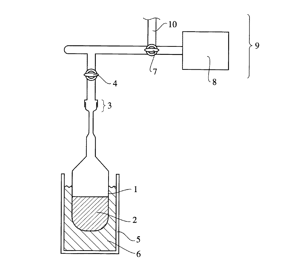
表1より、塗布液の脱酸素処理を行っていない比較例1の発光素子と比較して、本発明の製造方法によって得られる実施例1及び2の発光素子は優れた発光輝度及び発光効率を示すことがわかる。
【0063】
【発明の効果】
以上詳述したように、三重項励起子を有効に利用した本発明の製造方法によって得られる発光素子は、発光効率、発光輝度及び耐久性に優れ、製造コストが低く、且つ大面積化が可能であるためにフルカラーディスプレイ、バックライト、照明光源等の面光源、プリンター等の光源アレイ等に有効に利用できる。
【図面の簡単な説明】
【図1】 本発明で用いる塗布液の脱酸素処理を行うための装置の一例を示す概略図である。
【符号の説明】
1・・・フラスコ
2・・・塗布液
3・・・すりあわせ部
4・・・コック
5・・・ジュワー瓶
6・・・液体窒素
7・・・コック
8・・・真空ポンプ
9・・・真空ライン
10・・・窒素ライン[0001]
BACKGROUND OF THE INVENTION
The present invention relates to a light-emitting element that is excellent in light emission luminance and light emission efficiency and can be manufactured at low cost, and a method for manufacturing the same.
[0002]
[Prior art]
Organic light-emitting devices using organic materials are promising for use as solid light-emitting inexpensive large-area full-color display devices and writing light source arrays, and active research and development have been promoted in recent years. In general, an organic light emitting device is composed of an organic compound layer including a light emitting layer and a pair of counter electrodes sandwiching the organic compound layer. When a voltage is applied to such an organic light emitting device, electrons are injected from the cathode and holes are injected from the anode into the organic compound layer. The electrons and holes recombine in the light emitting layer, and light is emitted by releasing energy as light when the energy level returns from the conduction band to the valence band.
[0003]
Conventional organic light emitting devices have a problem of high driving voltage and low light emission luminance and light emission efficiency. In recent years, various techniques for solving this problem have been reported. For example, an organic light emitting device having an organic thin film formed by vapor deposition of an organic compound is known (Applied Physics Letters, 51, 913, 1987). ). This organic light-emitting device has a laminated two-layer structure of an electron transport layer made of an electron transport material and a hole transport layer made of a hole transport material, and exhibits significantly improved light emission characteristics as compared with a single layer type device. A low molecular amine compound is used as the hole transport material, and an aluminum complex (Alq) of 8-quinolinol is used as the electron transport material and light emitting material, and the emission color is green. Many organic light-emitting devices having a vapor-deposited organic thin film have been reported since then (see the references described in Macromolecular Symposium, Vol. 125,
[0004]
Most of the conventional organic light-emitting elements utilize fluorescence emitted from singlet excitons of organic light-emitting materials. In the mechanism of simple quantum chemistry, the ratio of singlet excitons capable of obtaining fluorescence in the exciton state and triplet excitons capable of obtaining phosphorescence is 1: 3. That is, as long as fluorescence emission is used, only 25% of excitons can be effectively used, and the emission efficiency of the fluorescence element is low. Under such circumstances, a phosphorescent light emitting device using a phenylpyridine complex of iridium was recently reported (Applied Physics Letter, 75, 4 pages, 1999, Japanese Journal of Applied Physics, 38, L1502, 1999). Year). This phosphorescent light-emitting device exhibits a
[0005]
On the other hand, when forming an organic compound layer of an organic light emitting device, various methods such as a vapor deposition method, a sputtering method, CVD, PVD, and a coating method using a solvent can be used. From the viewpoint of simplification of the process, reduction of manufacturing cost, improvement of workability, and application to flexible large-area elements such as a backlight and an illumination light source, a wet film forming method such as a coating method is advantageous. Several organic light-emitting devices in which a polymer compound is formed by a wet film-forming method have already been reported. As the polymer compound, polyparaphenylene vinylene that emits green light (Nature, 347, 539, 1990) , Poly (3-alkylthiophene) that emits red-orange light (Japanese Journal of Applied Physics, 30, L1938, 1991), Polyalkylfluorene that exhibits blue light emission (Japanese Journal of Applied Physics, 30, L1941, 1991). Japanese Patent Laid-Open No. 2-223188 reports a method of dispersing a low molecular compound in a binder resin and forming a film by wet coating. However, all these wet-type film-forming elements utilize singlet excitons, and the fundamental problem that the light emission efficiency is low remains.
[0006]
[Problems to be solved by the invention]
The object of the present invention is excellent in light emission luminance and light emission efficiency, low in manufacturing cost, and capable of increasing the area, and thus effective for surface light sources such as full-color displays, backlights and illumination light sources, and light source arrays such as printers. It is providing the light emitting element which can be utilized for.
[0007]
[Means for Solving the Problems]
As a result of diligent research in view of the above problems, the present inventors have found that phosphorescent light-emitting devices using triplet excitons are more susceptible to oxygen than fluorescent light-emitting devices using singlet excitons, and quenching phenomenon due to oxygen. The present inventors have found that a phosphorescent light emitting device having excellent light emitting characteristics can be obtained by forming an organic compound layer using a coating solution that has been deoxygenated in advance, and have arrived at the present invention.
[0008]
That is, the production method of the present invention is a substrate, a transparent electrode, a method of manufacturing a light emitting element that have a least one layer of the organic compound layer and the back electrode including a light emitting layer, the light-emitting layer containing a phosphorescent compound Then , the light emitting layer is subjected to oxygen deoxidation by at least one method selected from a deoxygenation method by heating, a deoxygenation method by vacuum, a deoxygenation method by bubbling of an inert gas, and a deoxygenation method by a separation membrane. gas dissolution concentration is characterized in that a film by a wet film-forming method using a coating solution deoxygenated to 100ppm or less. The light-emitting element obtained by the manufacturing method of the present invention is excellent in light emission luminance and light emission efficiency, can be manufactured at low cost, and can have a large area, so that it is a surface light source such as a full-color display, a backlight, and an illumination light source. It can be effectively used for light source arrays such as printers.
[0010]
DETAILED DESCRIPTION OF THE INVENTION
The light emitting device obtained by the production method of the present invention is formed by laminating a transparent electrode, one or more organic compound layers and a back electrode on a substrate. The organic compound layer includes a light emitting layer, and the light emitting layer contains a phosphorescent compound. You may have organic compound layers other than a light emitting layer, a protective layer, etc. as needed. In the production method of the present invention, a light emitting layer, forming a film by a wet film-forming method using deoxygenated coating solution.
[0011]
The structure of the light emitting device of the present invention is as follows: transparent electrode / light emitting layer / back electrode, transparent electrode / light emitting layer / electron transport layer / back electrode, transparent electrode / hole transport layer / light emitting layer / electron transport layer / Back electrode, transparent electrode / hole transport layer / light emitting layer / back electrode, transparent electrode / light emitting layer / electron transport layer / electron injection layer / back electrode, transparent electrode / hole injection layer / hole transport layer / light emitting layer / A configuration in which the electron transport layer / electron injection layer / back electrode and the like are stacked in this order, or a configuration in which these are stacked in reverse may be used. The light emitting layer contains a phosphorescent compound, and light is usually extracted from the transparent electrode. Specific examples of the compound used for each layer are described in, for example, “Monthly Display”, October 1998 issue “Organic EL Display” (Techno Times).
[0012]
The formation position of the organic compound layer is not particularly limited and can be appropriately selected depending on the use and purpose of the light-emitting element, but is preferably formed on the transparent electrode or the back electrode. At this time, the organic compound layer may be formed on the entire surface or a part of the transparent electrode or the back electrode. The shape, size and thickness of the organic compound layer can also be appropriately selected according to the purpose.
[0013]
The organic compound layer may be formed by a dry film forming method or a wet film forming method. However, when the wet film forming method is used, the organic compound layer can be easily increased in area, and has high luminance and excellent luminous efficiency. A light-emitting element is preferable because it can be efficiently obtained at low cost. Vapor deposition, sputtering, etc. can be used as dry film forming methods, and dipping method, spin coating method, dip coating method, casting method, die coating method, roll coating method, bar coating method, gravure coating method as wet film forming methods. Etc. can be used. These film forming methods can be appropriately selected according to the material of the organic compound layer. When the film is formed by a wet film forming method, it may be dried after the film is formed. Drying is performed by selecting conditions such as temperature and pressure so that the coating layer is not damaged.
[0014]
In the present invention, a light emitting layer, forming a film by a wet film-forming method using deoxygenated coating solution. By deoxidizing the coating solution before film formation, oxygen gas that significantly deteriorates the light emission characteristics of the phosphorescent light emitting element can be removed. That is, in the present invention, the amount of oxygen remaining in the light-emitting layer is greatly reduced by wet-forming the light-emitting layer using a coating solution that has been deoxygenated in advance, thereby improving the light-emitting luminance, light-emitting efficiency, and durability of the device. Can be improved.
[0015]
The coating solution usually comprises a material for the organic compound layer and a solvent for dissolving or dispersing it. A solvent is not specifically limited, What is necessary is just to select according to the material used for an organic compound layer. Specific examples of solvents include halogen solvents (chloroform, carbon tetrachloride, dichloromethane, 1,2-dichloroethane, chlorobenzene, etc.), ketone solvents (acetone, methyl ethyl ketone, diethyl ketone, n-propyl methyl ketone, cyclohexanone, etc.), Aromatic solvents (benzene, toluene, xylene, etc.), ester solvents (ethyl acetate, n-propyl acetate, n-butyl acetate, methyl propionate, ethyl propionate, γ-butyrolactone, diethyl carbonate, etc.), ether solvents (Tetrahydrofuran, dioxane, etc.), amide solvents (dimethylformamide, dimethylacetamide, etc.), dimethyl sulfoxide, water and the like. The solid content with respect to the solvent in the coating solution is not particularly limited, and the viscosity of the coating solution can be arbitrarily selected according to the film forming method.
[0016]
The deoxygenation method is not particularly limited as long as it does not cause deterioration of the coating solution. Deoxygenation method by heating, deoxygenation method by vacuum, deoxygenation method by bubbling of inert gas, separation membrane Can be used. The deoxygenation treatment may be performed so that the concentration of dissolved oxygen gas in the coating solution is 100 ppm or less. The dissolved oxygen gas concentration is preferably 50 ppm or less, and more preferably 30 ppm or less.
[0017]
FIG. 1 is a schematic view showing an example of an apparatus for performing deoxygenation using a vacuum line. Hereinafter, an embodiment of the deoxygenation process using a vacuum line will be described with reference to FIG. First, the
[0018]
The light emitting device obtained by the production method of the present invention usually emits light when a DC voltage (which may include an AC component) or a DC current of about 2 to 40 volts is applied between the transparent electrode and the back electrode. When driving a light emitting element, JP-A-2-148687, JP-A-6-301355, JP-A-5-29080, JP-A-7-34558, JP-A-8-234685, JP-A-8-241047, U.S. Patents The driving methods described in Japanese Patent Nos. 5828429, 6023308, and Japanese Patent No. 2784615 can be used. Hereinafter, although each element which comprises the light emitting element obtained by the manufacturing method of this invention is explained in full detail, this invention is not limited by them.
[0019]
(A) Base material The base material used in the present invention is an inorganic material such as zirconia stabilized yttrium (YSZ), glass, polyester such as polyethylene terephthalate, polybutylene terephthalate, polyethylene naphthalate, polystyrene, polycarbonate, polyethersulfone, It may be made of a polymer material such as polyarylate, allyl diglycol carbonate, polyimide, polycycloolefin, norbornene resin, poly (chlorotrifluoroethylene), Teflon, polytetrafluoroethylene-polyethylene copolymer, and the like. The substrate may be formed of a single material or two or more materials. Among these, in order to form a flexible light-emitting element, a polymer material is preferable, polyester having excellent heat resistance, dimensional stability, solvent resistance, electrical insulation and workability, and low air permeability and low moisture absorption, Polymer materials containing fluorine atoms such as polycarbonate, polyethersulfone, poly (chlorotrifluoroethylene), Teflon, and polytetrafluoroethylene-polyethylene copolymer are more preferable.
[0020]
The shape, structure, size, and the like of the substrate can be appropriately selected according to the use and purpose of the light emitting element. The shape is generally plate-like. The structure may be a single layer structure or a laminated structure. The substrate may be colorless and transparent or colored and transparent, but is preferably colorless and transparent in that it does not scatter or attenuate light emitted from the light emitting layer.
[0021]
A moisture permeation preventing layer (gas barrier layer) may be provided on the electrode-side surface of the substrate, the surface opposite to the electrode, or both. As a material constituting the moisture permeation preventing layer, it is preferable to use an inorganic material such as silicon nitride or silicon oxide. The moisture permeation preventing layer can be formed by a high frequency sputtering method or the like. Moreover, you may provide a hard-coat layer and an undercoat layer in a base material as needed.
[0022]
(B) Transparent electrode Normally, the transparent electrode functions as an anode for supplying holes to the organic compound layer, but it can also function as a cathode. In this case, the back electrode functions as an anode. Hereinafter, the case where a transparent electrode is used as an anode will be described.
[0023]
The shape, structure, size, and the like of the transparent electrode are not particularly limited, and can be appropriately selected according to the use and purpose of the light emitting element. As a material for forming the transparent electrode, a metal, an alloy, a metal oxide, an electrically conductive compound, a mixture thereof, or the like can be used, and a material having a work function of 4 eV or more is preferably used. Specific examples include tin oxide doped with antimony (ATO), tin oxide doped with fluorine (FTO), semiconductive metal oxides (tin oxide, zinc oxide, indium oxide, indium tin oxide (ITO), zinc oxide) Indium (IZO, etc.), metals (gold, silver, chromium, nickel, etc.), mixtures or laminates of these metals and conductive metal oxides, inorganic conductive substances (copper iodide, copper sulfide, etc.), organic conductivity Materials (polyaniline, polythiophene, polypyrrole, etc.) and laminates of this and ITO.
[0024]
The transparent electrode can be formed on the substrate by a wet method such as a printing method or a coating method, a physical method such as a vacuum deposition method, a sputtering method or an ion plating method, or a chemical method such as a CVD or plasma CVD method. it can. The formation method may be appropriately selected in consideration of suitability with the transparent electrode material. For example, when ITO is used as the material for the transparent electrode, a direct current or high frequency sputtering method, a vacuum deposition method, an ion plating method, or the like may be used. Further, when an organic conductive material is used as the material for the transparent electrode, a wet film forming method may be used.
[0025]
The patterning of the transparent electrode can be performed by chemical etching using photolithography, physical etching using a laser, or the like. Alternatively, patterning may be performed by vacuum deposition using a mask, sputtering, a lift-off method, a printing method, or the like.
[0026]
The formation position of the transparent electrode may be appropriately selected according to the use and purpose of the light-emitting element, but is preferably formed on the substrate. At this time, the transparent electrode may be formed on the entire surface of the substrate or only on a part thereof.
[0027]
The thickness of the transparent electrode may be appropriately selected according to the material, but is usually 10 nm to 50 μm, preferably 50 nm to 20 μm. The resistance value of the transparent electrode is preferably 10 3 Ω / □ or less, and more preferably 10 2 Ω / □ or less. The transparent electrode may be colorless and transparent or colored and transparent. In order to extract emitted light from the transparent electrode side, the transmittance is preferably 60% or more, and more preferably 70% or more. The transmittance can be measured according to a known method using a spectrophotometer.
[0028]
Electrodes described in detail in “New development of transparent conductive film” (supervised by Yutaka Sawada, published by CMC, 1999) can also be applied to the present invention. In particular, when using a plastic substrate having low heat resistance, it is preferable to use ITO or IZO as the transparent electrode material and to form a film at a low temperature of 150 ° C. or lower.
[0029]
(C) Back electrode Normally, the back electrode functions as a cathode for injecting electrons into the organic compound layer, but it can also function as an anode. In this case, the transparent electrode functions as a cathode. Hereinafter, a case where the back electrode is a cathode will be described.
[0030]
The shape, structure, size, and the like of the back electrode are not particularly limited, and can be appropriately selected according to the use and purpose of the light emitting element. As a material for forming the back electrode, a metal, an alloy, a metal oxide, an electrically conductive compound, a mixture thereof, or the like can be used, and a material having a work function of 4.5 eV or less is preferably used. Specific examples include alkali metals (Li, Na, K, Cs, etc.), alkaline earth metals (Mg, Ca, etc.), gold, silver, lead, aluminum, sodium-potassium alloy, lithium-aluminum alloy, magnesium-silver. Examples include alloys, indium, rare earth metals (ytterbium, etc.). These may be used alone, but in order to achieve both stability and electron injection properties, it is preferable to use two or more in combination. Among these materials, alkali metals and alkaline earth metals are preferable from the viewpoint of electron injecting property, and materials mainly composed of aluminum are preferable from the viewpoint of storage stability. Here, the material mainly composed of aluminum refers to aluminum alone, an alloy or a mixture of aluminum and 0.01 to 10% by mass of an alkali metal or alkaline earth metal. As materials for the back electrode, those described in detail in JP-A-2-15595, JP-A-5-121172 and the like can be used.
[0031]
The back electrode can be formed by a wet method such as a printing method or a coating method, a physical method such as a vacuum deposition method, a sputtering method or an ion plating method, or a chemical method such as a CVD or plasma CVD method. The formation method may be appropriately selected in consideration of suitability with the back electrode material. For example, when two or more metals are used as the back electrode material, the materials can be formed by sputtering simultaneously or sequentially.
[0032]
The back electrode can be patterned by chemical etching using photolithography or the like, physical etching using a laser, or the like. Alternatively, patterning may be performed by vacuum deposition using a mask, sputtering, a lift-off method, a printing method, or the like.
[0033]
The formation position of the back electrode may be appropriately selected according to the use and purpose of the light emitting element, but is preferably formed on the organic compound layer. At this time, the back electrode may be formed on the entire surface of the organic compound layer or only on a part thereof. Further, a dielectric layer made of an alkali metal or alkaline earth metal fluoride or the like may be provided between the back electrode and the organic compound layer with a thickness of 0.1 to 5 nm. The dielectric layer can be formed by a vacuum deposition method, a sputtering method, an ion plating method, or the like.
[0034]
The thickness of the back electrode may be appropriately selected depending on the material, but is usually 10 nm to 5 μm, preferably 50 nm to 1 μm. The back electrode may be transparent or opaque. The transparent back electrode can be formed by thinly forming the above-described material layer to a thickness of 1 to 10 nm and further laminating a transparent conductive material such as ITO or IZO.
[0035]
(D) Light emitting layer
In the light-emitting element , the light-emitting layer contains a phosphorescent compound. The phosphorescent compound is not particularly limited as long as it is a compound that can emit light from triplet excitons. As the phosphorescent compound, an orthometalated complex or a porphyrin complex is preferably used, and an orthometalated complex is more preferably used. Of the porphyrin complexes, a porphyrin platinum complex is preferred. The phosphorescent compounds may be used alone or in combination of two or more.
[0036]
The ortho-metalated complex referred to in the present invention is “Photometal and Photophysics of Coordination Compounds” written by Akio Yamamoto, “Basics and Applications of Organometallic Chemistry”, pages 150 and 232, Houbobo (1982), H. Yersin. 71-77 and 135-146, Springer-Verlag (1987), etc. The ligand forming the orthometalated complex is not particularly limited, but 2-phenylpyridine derivative, 7,8-benzoquinoline derivative, 2- (2-thienyl) pyridine derivative, 2- (1-naphthyl) pyridine derivative or A 2-phenylquinoline derivative is preferred. These derivatives may have a substituent. Moreover, you may have another ligand other than these essential ligands for ortho metalation complex formation. As the central metal forming the orthometalated complex, any transition metal can be used. In the present invention, rhodium, platinum, gold, iridium, ruthenium, palladium and the like can be preferably used. Of these, iridium is particularly preferred. An organic compound layer containing such an orthometalated complex is excellent in light emission luminance and light emission efficiency. Specific examples of the orthometalated complex are also described in paragraphs 0152 to 0180 of Japanese Patent Application No. 2000-254171.
[0037]
The orthometalated complexes used in the present invention are Inorg. Chem., 30, 1685, 1991, Inorg. Chem., 27, 3464, 1988, Inorg. Chem., 33, 545, 1994, Inorg. Chim. Acta, 181. , 245, 1991, J. Organomet. Chem., 335, 293, 1987, J. Am. Chem. Soc., 107, 1431, 1985, and the like.
[0038]
Although content in particular of the phosphorescence-emitting compound in a light emitting layer is not restrict | limited, For example, it is 0.1-70 mass%, and it is preferable that it is 1-20 mass%. If the content of the phosphorescent compound is less than 0.1% by mass or exceeds 70% by mass, the effect may not be sufficiently exhibited.
[0039]
In the present invention, the light emitting layer may contain a host compound, a hole transport material, an electron transport material, an electrically inactive polymer binder, and the like, if necessary.
[0040]
The host compound is a compound that causes energy transfer from the excited state to the phosphorescent compound, and as a result, causes the phosphorescent compound to emit light. Specific examples include carbazole derivatives, triazole derivatives, oxazole derivatives, oxadiazole derivatives, imidazole derivatives, polyarylalkane derivatives, pyrazoline derivatives, pyrazolone derivatives, phenylenediamine derivatives, arylamine derivatives, amino-substituted chalcone derivatives, styrylanthracene derivatives. , Fluorenone derivatives, hydrazone derivatives, stilbene derivatives, silazane derivatives, aromatic tertiary amine compounds, styrylamine compounds, aromatic dimethylidene compounds, porphyrin compounds, anthraquinodimethane derivatives, anthrone derivatives, diphenylquinone derivatives, thiopyran dioxide oxide Derivatives, carbodiimide derivatives, fluorenylidenemethane derivatives, distyrylpyrazine derivatives, and heterocyclic tetra Rubonic anhydride, phthalocyanine derivative, metal complex of 8-quinolinol derivative, metal phthalocyanine, metal complex having benzoxazole or benzothiazole as a ligand, polysilane compound, poly (N-vinylcarbazole) derivative, aniline copolymer , Conductive polymers such as thiophene oligomers and polythiophenes, polythiophene derivatives, polyphenylene derivatives, polyphenylene vinylene derivatives, polyfluorene derivatives, and the like. A host compound may be used individually by 1 type, or may use 2 or more types together.
[0041]
The hole transport material is not particularly limited as long as it has any of the function of injecting holes from the anode, the function of transporting holes, and the function of blocking electrons injected from the cathode. It may be a molecular material or a polymer material. Specific examples include carbazole derivatives, triazole derivatives, oxazole derivatives, oxadiazole derivatives, imidazole derivatives, polyarylalkane derivatives, pyrazoline derivatives, pyrazolone derivatives, phenylenediamine derivatives, arylamine derivatives, amino-substituted chalcone derivatives, styrylanthracene derivatives. Fluorenone derivatives, hydrazone derivatives, stilbene derivatives, silazane derivatives, aromatic tertiary amine compounds, styrylamine compounds, aromatic dimethylidene compounds, porphyrin compounds, polysilane compounds, poly (N-vinylcarbazole) derivatives, aniline copolymers, Conductive polymers such as thiophene oligomers and polythiophenes, polythiophene derivatives, polyphenylene derivatives, polyphenylene vinylene derivatives, polyfluorenes Derivatives and the like. These may be used alone or in combination of two or more.
[0042]
The electron transport material is not particularly limited as long as it has any of the function of injecting electrons from the cathode, the function of transporting electrons, and the function of blocking holes injected from the anode. For example, a triazole derivative , Oxazole derivatives, oxadiazole derivatives, fluorenone derivatives, anthraquinodimethane derivatives, anthrone derivatives, diphenylquinone derivatives, thiopyran dioxide derivatives, carbodiimide derivatives, fluorenylidenemethane derivatives, distyrylpyrazine derivatives, naphthaleneperylene, Ring tetracarboxylic acid anhydrides, phthalocyanine derivatives, metal complexes of 8-quinolinol derivatives, metal complexes with metallophthalocyanine, benzoxazole, benzothiazole, etc., aniline copolymers, thiophene oligomers, polythiophenes, etc. Conductive polymer, polythiophene derivatives, polyphenylene derivatives, polyphenylene vinylene derivatives, polyfluorene derivatives and the like can be used.
[0043]
Polymer binders include polyvinyl chloride, polycarbonate, polystyrene, polymethyl methacrylate, polybutyl methacrylate, polyester, polysulfone, polyphenylene oxide, polybutadiene, hydrocarbon resin, ketone resin, phenoxy resin, polyamide, ethyl cellulose, vinyl acetate, ABS resin, Polyurethane, melamine resin, unsaturated polyester, alkyd resin, epoxy resin, silicone resin, polyvinyl butyral, polyvinyl acetal, etc. can be used. The light emitting layer containing the polymer binder can be easily applied and formed in a large area by a wet film forming method.
[0044]
The thickness of the light emitting layer is preferably 10 to 200 nm, and more preferably 20 to 80 nm. When the thickness exceeds 200 nm, the driving voltage may increase, and when it is less than 10 nm, the light emitting element may be short-circuited.
[0045]
(E) Electron transport layer
The light emitting element may have an electron transport layer made of the above-described electron transport material as necessary. The electron transport layer may contain the polymer binder described above. The thickness of the electron transport layer is preferably 10 to 200 nm, and more preferably 20 to 80 nm. When the thickness exceeds 200 nm, the driving voltage may increase, and when it is less than 10 nm, the light emitting element may be short-circuited.
[0046]
(F) Hole transport layer
The light emitting element may have a hole transport layer made of the above-described hole transport material, if necessary. The hole transport layer may contain the polymer binder described above. The thickness of the hole transport layer is preferably 10 to 200 nm, and more preferably 20 to 80 nm. When the thickness exceeds 200 nm, the driving voltage may increase, and when it is less than 10 nm, the light emitting element may be short-circuited.
[0047]
(G) Other
The light emitting element may have a protective layer described in JP-A-7-85974, JP-A-7-192866, JP-A-8-22891, JP-A-10-275682, JP-A-10-106746, and the like. The protective layer is formed on the uppermost surface of the light emitting element. Here, the top surface refers to the outer surface of the back electrode when the base material, the transparent electrode, the organic compound layer, and the back electrode are laminated in this order, and the base material, the back electrode, the organic compound layer, and the transparent electrode in this order. When laminating, it refers to the outer surface of the transparent electrode. The shape, size, thickness and the like of the protective layer are not particularly limited. The material for forming the protective layer is not particularly limited as long as it has a function of suppressing intrusion or permeation of a light-emitting element such as moisture or oxygen into the element. Silicon, germanium oxide, germanium dioxide or the like can be used.
[0048]
The method for forming the protective layer is not particularly limited. For example, vacuum deposition method, sputtering method, reactive sputtering method, molecular sensing epitaxy method, cluster ion beam method, ion plating method, plasma polymerization method, plasma CVD method, laser CVD method Thermal CVD method, coating method, etc. can be applied.
[0049]
In addition, the light-emitting element is preferably provided with a sealing layer for preventing moisture and oxygen from entering. As a material for forming the sealing layer, a copolymer of tetrafluoroethylene and at least one comonomer, a fluorinated copolymer having a cyclic structure in the copolymer main chain, polyethylene, polypropylene, polymethyl methacrylate, polyimide, Polyurea, polytetrafluoroethylene, polychlorotrifluoroethylene, polydichlorodifluoroethylene, chlorotrifluoroethylene or a copolymer of dichlorodifluoroethylene and other comonomers, water-absorbing substance with a water absorption of 1% or more, water absorption of 0.1% The following moisture-proof materials, metals (In, Sn, Pb, Au, Cu, Ag, Al, Tl, Ni, etc.), metal oxides (MgO, SiO, SiO 2 , Al 2 O 3 , GeO, NiO, CaO, BaO, Fe 2 O 3, Y 2 O 3,
[0050]
In order to block moisture and oxygen from the outside, it is preferable to seal the light emitting element with a sealing plate, a sealing container, or the like using a sealing agent. As a material used for the sealing plate, the sealing container, etc., glass, stainless steel, metal (aluminum, etc.), plastic (poly (chlorotrifluoroethylene), polyester, polycarbonate, etc.), ceramic, etc. can be used. As the sealant, an ultraviolet curable resin, a thermosetting resin, a two-component curable resin, or the like can be used.
[0051]
Furthermore, in the present invention, a moisture absorbent or an inert liquid may be inserted into the space between the sealing container and the light emitting element. The moisture absorbent is not particularly limited, and specific examples include barium oxide, sodium oxide, potassium oxide, calcium oxide, sodium sulfate, calcium sulfate, magnesium sulfate, phosphorus pentoxide, calcium chloride, magnesium chloride, copper chloride, cesium fluoride. , Niobium fluoride, calcium bromide, vanadium bromide, molecular sieve, zeolite, magnesium oxide and the like. As the inert liquid, paraffins, liquid paraffins, fluorinated solvents (perfluoroalkane, perfluoroamine, perfluoroether, etc.), chlorinated solvents, silicone oils, and the like can be used.
[0052]
【Example】
EXAMPLES Hereinafter, although an Example demonstrates this invention further in detail, this invention is not limited to them.
[0053]
Example 1
A glass plate having a thickness of 0.2 mm was cut into 2.5 cm square to produce a substrate, which was introduced into a vacuum chamber. An ITO transparent electrode was formed on this substrate by DC magnetron sputtering (conditions: substrate temperature 100 ° C.,
[0054]
The substrate on which the transparent electrode was formed was placed in a cleaning container and subjected to IPA cleaning, and then UV-ozone treatment was performed for 30 minutes. Subsequently, poly (ethylenedioxythiophene) / polystyrenesulfonic acid aqueous dispersion (BAYER, Baytron P: 1.3% solid content) was spin-coated on the transparent electrode, and vacuum dried at 150 ° C. for 2 hours to a thickness of 100 nm. The hole injection layer was formed.
[0055]
Next, polyvinylcarbazole (Mw = 63000, manufactured by Aldrich, hole transport material and host material), tris (2-phenylpyridine) iridium complex (phosphorescent material), and 2- (4-biphenylyl) -5- (4 -t-Butylphenyl) -1,3,4-oxadiazole (PBD, electron transport material) was dissolved in dichloroethane at a mass ratio of 40: 1: 12 to prepare a coating solution.
[0056]
The obtained coating solution was deoxygenated using the apparatus shown in FIG. First, the
[0057]
The deoxygenated coating solution was applied onto the hole injection layer using a spin coater and dried at room temperature to form a light emitting layer having a thickness of 100 nm. Furthermore, a patterned mask (a mask with a light emitting area of 5 mm × 5 mm) is placed on the light emitting layer, and a magnesium / silver alloy (magnesium: silver = 10: 1 (molar ratio)) is deposited by 0.25 μm in a vapor deposition apparatus. Then, silver was deposited by 0.3 μm to form a back electrode. Aluminum lead wires were connected from the transparent electrode and the back electrode to form a laminated structure. The laminated structure is put in a glove box substituted with nitrogen gas, and sealed with a glass sealing container using an ultraviolet curable adhesive (XNR5493, manufactured by CHI Nagase) to produce the light emitting device of Example 1. did.
[0058]
Example 2
2,2 ', 2''-(1,3,5-Benzenetriyl) tris [3- (2-methylphenyl) -3H-imidazo [4,5-b] pyridine] on the light-emitting layer was 1 nm / The light emitting device of Example 2 was fabricated in the same manner as in Example 1 except that an electron transport layer having a thickness of 0.024 μm was provided by vapor deposition at a rate of 2 seconds, and a back electrode was provided thereon.
[0059]
Comparative Example 1
A light emitting device of Comparative Example 1 was prepared in the same manner as Example 1 except that the coating liquid was not subjected to deoxygenation treatment.
[0060]
Evaluation of light emission luminance and light emission efficiency Using a source measure unit type 2400 manufactured by Toyo Technica, a direct current voltage was applied to each light emitting element obtained as described above to emit light, and the luminance was measured. Maximum luminance L max, the maximum brightness voltage V max when L max is obtained, luminous efficiency eta 200 when light is emitted at luminance 200 cd / m 2 of each light-emitting element, light emission when light is emitted at a luminance 2000 cd / m 2 The efficiency η 2000 (external quantum efficiency) is also shown in Table 1.
[0061]
[Table 1]
From Table 1, the light emitting elements of Examples 1 and 2 obtained by the production method of the present invention have superior light emission luminance and light emission efficiency as compared with the light emitting element of Comparative Example 1 in which the coating liquid was not subjected to deoxygenation treatment. You can see that
[0063]
【The invention's effect】
As described above in detail, the light-emitting element obtained by the manufacturing method of the present invention that effectively uses triplet excitons is excellent in light emission efficiency, light emission luminance, and durability, has low manufacturing cost, and can have a large area. Therefore, it can be effectively used for a full-color display, a backlight, a surface light source such as an illumination light source, a light source array such as a printer, and the like.
[Brief description of the drawings]
FIG. 1 is a schematic view showing an example of an apparatus for performing a deoxygenation treatment of a coating solution used in the present invention.
[Explanation of symbols]
DESCRIPTION OF
10 ... Nitrogen line
Claims (3)
Priority Applications (1)
| Application Number | Priority Date | Filing Date | Title |
|---|---|---|---|
| JP2000364649A JP4119084B2 (en) | 2000-11-30 | 2000-11-30 | Method for manufacturing light emitting device |
Applications Claiming Priority (1)
| Application Number | Priority Date | Filing Date | Title |
|---|---|---|---|
| JP2000364649A JP4119084B2 (en) | 2000-11-30 | 2000-11-30 | Method for manufacturing light emitting device |
Publications (3)
| Publication Number | Publication Date |
|---|---|
| JP2002170677A JP2002170677A (en) | 2002-06-14 |
| JP2002170677A5 JP2002170677A5 (en) | 2005-11-04 |
| JP4119084B2 true JP4119084B2 (en) | 2008-07-16 |
Family
ID=18835553
Family Applications (1)
| Application Number | Title | Priority Date | Filing Date |
|---|---|---|---|
| JP2000364649A Expired - Lifetime JP4119084B2 (en) | 2000-11-30 | 2000-11-30 | Method for manufacturing light emitting device |
Country Status (1)
| Country | Link |
|---|---|
| JP (1) | JP4119084B2 (en) |
Families Citing this family (4)
| Publication number | Priority date | Publication date | Assignee | Title |
|---|---|---|---|---|
| JP4195411B2 (en) | 2004-04-12 | 2008-12-10 | セイコーエプソン株式会社 | Method for manufacturing organic electroluminescence device |
| DE102005022903A1 (en) * | 2005-05-18 | 2006-11-23 | Merck Patent Gmbh | Solutions of organic semiconductors |
| US20140020760A1 (en) * | 2011-02-28 | 2014-01-23 | Sumitomo Chemical Company, Limited | Method of producing organic photoelectric conversion device |
| JP6380692B2 (en) | 2016-01-28 | 2018-08-29 | 住友化学株式会社 | Membrane manufacturing method |
-
2000
- 2000-11-30 JP JP2000364649A patent/JP4119084B2/en not_active Expired - Lifetime
Also Published As
| Publication number | Publication date |
|---|---|
| JP2002170677A (en) | 2002-06-14 |
Similar Documents
| Publication | Publication Date | Title |
|---|---|---|
| JP3942017B2 (en) | Light emitting element | |
| JP4112800B2 (en) | Light emitting device and manufacturing method thereof | |
| US6853013B2 (en) | Light-emitting element and method of producing the same | |
| JP4040249B2 (en) | Light emitting element | |
| JP4010845B2 (en) | Light emitting element | |
| US20040164671A1 (en) | Organic light emitting diode | |
| JP2004296219A (en) | Light emitting element | |
| JP2004055333A (en) | Coating liquid for light emitting element and manufacturing method of light emitting element | |
| JP4578642B2 (en) | Organic light emitting device | |
| JP2003133080A (en) | Light emitting element | |
| JP2002246172A (en) | Light-emitting element and manufacturing method for the same | |
| JP4119084B2 (en) | Method for manufacturing light emitting device | |
| JP2002246184A (en) | Light-emitting element | |
| KR100998460B1 (en) | Organic electroluminescent element | |
| JP2002050482A (en) | Organic light emission element | |
| JP5473705B2 (en) | Organic electroluminescent device and method for producing organic electroluminescent device | |
| JP2002180040A (en) | Luminescent device | |
| US7749616B2 (en) | Organic electroluminescent element and display device using the same | |
| JP2002175882A (en) | Luminous element | |
| JP4307793B2 (en) | Method for manufacturing light emitting device | |
| JP2005100767A (en) | Organic electroluminescent element | |
| JP4112799B2 (en) | Light emitting device and manufacturing method thereof | |
| JP2002170676A (en) | Luminescent element and its manufacturing method | |
| JP2002175881A (en) | Light emitting element | |
| JP2003100448A (en) | Light emitting element |
Legal Events
| Date | Code | Title | Description |
|---|---|---|---|
| A521 | Request for written amendment filed |
Free format text: JAPANESE INTERMEDIATE CODE: A523 Effective date: 20050913 |
|
| A621 | Written request for application examination |
Free format text: JAPANESE INTERMEDIATE CODE: A621 Effective date: 20050913 |
|
| A131 | Notification of reasons for refusal |
Free format text: JAPANESE INTERMEDIATE CODE: A131 Effective date: 20060712 |
|
| A521 | Request for written amendment filed |
Free format text: JAPANESE INTERMEDIATE CODE: A523 Effective date: 20060911 |
|
| A02 | Decision of refusal |
Free format text: JAPANESE INTERMEDIATE CODE: A02 Effective date: 20061122 |
|
| A711 | Notification of change in applicant |
Free format text: JAPANESE INTERMEDIATE CODE: A712 Effective date: 20061207 |
|
| A521 | Request for written amendment filed |
Free format text: JAPANESE INTERMEDIATE CODE: A523 Effective date: 20061222 |
|
| A911 | Transfer to examiner for re-examination before appeal (zenchi) |
Free format text: JAPANESE INTERMEDIATE CODE: A911 Effective date: 20070130 |
|
| A521 | Request for written amendment filed |
Free format text: JAPANESE INTERMEDIATE CODE: A523 Effective date: 20070322 |
|
| A911 | Transfer to examiner for re-examination before appeal (zenchi) |
Free format text: JAPANESE INTERMEDIATE CODE: A911 Effective date: 20070327 |
|
| A521 | Request for written amendment filed |
Free format text: JAPANESE INTERMEDIATE CODE: A821 Effective date: 20070322 |
|
| A912 | Re-examination (zenchi) completed and case transferred to appeal board |
Free format text: JAPANESE INTERMEDIATE CODE: A912 Effective date: 20070427 |
|
| A521 | Request for written amendment filed |
Free format text: JAPANESE INTERMEDIATE CODE: A523 Effective date: 20080325 |
|
| A61 | First payment of annual fees (during grant procedure) |
Free format text: JAPANESE INTERMEDIATE CODE: A61 Effective date: 20080424 |
|
| R150 | Certificate of patent or registration of utility model |
Free format text: JAPANESE INTERMEDIATE CODE: R150 Ref document number: 4119084 Country of ref document: JP Free format text: JAPANESE INTERMEDIATE CODE: R150 |
|
| FPAY | Renewal fee payment (event date is renewal date of database) |
Free format text: PAYMENT UNTIL: 20110502 Year of fee payment: 3 |
|
| FPAY | Renewal fee payment (event date is renewal date of database) |
Free format text: PAYMENT UNTIL: 20110502 Year of fee payment: 3 |
|
| FPAY | Renewal fee payment (event date is renewal date of database) |
Free format text: PAYMENT UNTIL: 20120502 Year of fee payment: 4 |
|
| R250 | Receipt of annual fees |
Free format text: JAPANESE INTERMEDIATE CODE: R250 |
|
| FPAY | Renewal fee payment (event date is renewal date of database) |
Free format text: PAYMENT UNTIL: 20130502 Year of fee payment: 5 |
|
| R250 | Receipt of annual fees |
Free format text: JAPANESE INTERMEDIATE CODE: R250 |
|
| S111 | Request for change of ownership or part of ownership |
Free format text: JAPANESE INTERMEDIATE CODE: R313113 |
|
| FPAY | Renewal fee payment (event date is renewal date of database) |
Free format text: PAYMENT UNTIL: 20130502 Year of fee payment: 5 |
|
| R350 | Written notification of registration of transfer |
Free format text: JAPANESE INTERMEDIATE CODE: R350 |
|
| R250 | Receipt of annual fees |
Free format text: JAPANESE INTERMEDIATE CODE: R250 |
|
| R250 | Receipt of annual fees |
Free format text: JAPANESE INTERMEDIATE CODE: R250 |
|
| R250 | Receipt of annual fees |
Free format text: JAPANESE INTERMEDIATE CODE: R250 |
|
| R250 | Receipt of annual fees |
Free format text: JAPANESE INTERMEDIATE CODE: R250 |
|
| R250 | Receipt of annual fees |
Free format text: JAPANESE INTERMEDIATE CODE: R250 |
|
| R250 | Receipt of annual fees |
Free format text: JAPANESE INTERMEDIATE CODE: R250 |
|
| R250 | Receipt of annual fees |
Free format text: JAPANESE INTERMEDIATE CODE: R250 |
|
| R250 | Receipt of annual fees |
Free format text: JAPANESE INTERMEDIATE CODE: R250 |
|
| EXPY | Cancellation because of completion of term |