JP4116301B2 - Plasma display device - Google Patents
Plasma display device Download PDFInfo
- Publication number
- JP4116301B2 JP4116301B2 JP2002035552A JP2002035552A JP4116301B2 JP 4116301 B2 JP4116301 B2 JP 4116301B2 JP 2002035552 A JP2002035552 A JP 2002035552A JP 2002035552 A JP2002035552 A JP 2002035552A JP 4116301 B2 JP4116301 B2 JP 4116301B2
- Authority
- JP
- Japan
- Prior art keywords
- capacitance
- node
- transistor
- resonance
- wiring
- Prior art date
- Legal status (The legal status is an assumption and is not a legal conclusion. Google has not performed a legal analysis and makes no representation as to the accuracy of the status listed.)
- Expired - Fee Related
Links
- 239000003990 capacitor Substances 0.000 claims description 138
- 238000011084 recovery Methods 0.000 claims description 60
- 230000005855 radiation Effects 0.000 description 29
- 238000010586 diagram Methods 0.000 description 20
- 230000003071 parasitic effect Effects 0.000 description 16
- 102100039169 [Pyruvate dehydrogenase [acetyl-transferring]]-phosphatase 1, mitochondrial Human genes 0.000 description 10
- 101710126534 [Pyruvate dehydrogenase [acetyl-transferring]]-phosphatase 1, mitochondrial Proteins 0.000 description 10
- 230000000694 effects Effects 0.000 description 5
- 230000005670 electromagnetic radiation Effects 0.000 description 3
- 230000005669 field effect Effects 0.000 description 3
- 230000000737 periodic effect Effects 0.000 description 2
- 230000001681 protective effect Effects 0.000 description 2
- 230000002441 reversible effect Effects 0.000 description 2
- 230000000630 rising effect Effects 0.000 description 2
- 102100039167 [Pyruvate dehydrogenase [acetyl-transferring]]-phosphatase 2, mitochondrial Human genes 0.000 description 1
- 101710106699 [Pyruvate dehydrogenase [acetyl-transferring]]-phosphatase 2, mitochondrial Proteins 0.000 description 1
- 230000002411 adverse Effects 0.000 description 1
- 239000013256 coordination polymer Substances 0.000 description 1
- 238000007599 discharging Methods 0.000 description 1
- 238000005401 electroluminescence Methods 0.000 description 1
- 239000004973 liquid crystal related substance Substances 0.000 description 1
- 239000000463 material Substances 0.000 description 1
- 229920006395 saturated elastomer Polymers 0.000 description 1
Images


Classifications
-
- G—PHYSICS
- G09—EDUCATION; CRYPTOGRAPHY; DISPLAY; ADVERTISING; SEALS
- G09G—ARRANGEMENTS OR CIRCUITS FOR CONTROL OF INDICATING DEVICES USING STATIC MEANS TO PRESENT VARIABLE INFORMATION
- G09G3/00—Control arrangements or circuits, of interest only in connection with visual indicators other than cathode-ray tubes
- G09G3/20—Control arrangements or circuits, of interest only in connection with visual indicators other than cathode-ray tubes for presentation of an assembly of a number of characters, e.g. a page, by composing the assembly by combination of individual elements arranged in a matrix no fixed position being assigned to or needed to be assigned to the individual characters or partial characters
- G09G3/22—Control arrangements or circuits, of interest only in connection with visual indicators other than cathode-ray tubes for presentation of an assembly of a number of characters, e.g. a page, by composing the assembly by combination of individual elements arranged in a matrix no fixed position being assigned to or needed to be assigned to the individual characters or partial characters using controlled light sources
- G09G3/28—Control arrangements or circuits, of interest only in connection with visual indicators other than cathode-ray tubes for presentation of an assembly of a number of characters, e.g. a page, by composing the assembly by combination of individual elements arranged in a matrix no fixed position being assigned to or needed to be assigned to the individual characters or partial characters using controlled light sources using luminous gas-discharge panels, e.g. plasma panels
- G09G3/288—Control arrangements or circuits, of interest only in connection with visual indicators other than cathode-ray tubes for presentation of an assembly of a number of characters, e.g. a page, by composing the assembly by combination of individual elements arranged in a matrix no fixed position being assigned to or needed to be assigned to the individual characters or partial characters using controlled light sources using luminous gas-discharge panels, e.g. plasma panels using AC panels
- G09G3/296—Driving circuits for producing the waveforms applied to the driving electrodes
- G09G3/2965—Driving circuits for producing the waveforms applied to the driving electrodes using inductors for energy recovery
-
- G—PHYSICS
- G09—EDUCATION; CRYPTOGRAPHY; DISPLAY; ADVERTISING; SEALS
- G09G—ARRANGEMENTS OR CIRCUITS FOR CONTROL OF INDICATING DEVICES USING STATIC MEANS TO PRESENT VARIABLE INFORMATION
- G09G3/00—Control arrangements or circuits, of interest only in connection with visual indicators other than cathode-ray tubes
- G09G3/20—Control arrangements or circuits, of interest only in connection with visual indicators other than cathode-ray tubes for presentation of an assembly of a number of characters, e.g. a page, by composing the assembly by combination of individual elements arranged in a matrix no fixed position being assigned to or needed to be assigned to the individual characters or partial characters
- G09G3/22—Control arrangements or circuits, of interest only in connection with visual indicators other than cathode-ray tubes for presentation of an assembly of a number of characters, e.g. a page, by composing the assembly by combination of individual elements arranged in a matrix no fixed position being assigned to or needed to be assigned to the individual characters or partial characters using controlled light sources
- G09G3/28—Control arrangements or circuits, of interest only in connection with visual indicators other than cathode-ray tubes for presentation of an assembly of a number of characters, e.g. a page, by composing the assembly by combination of individual elements arranged in a matrix no fixed position being assigned to or needed to be assigned to the individual characters or partial characters using controlled light sources using luminous gas-discharge panels, e.g. plasma panels
- G09G3/288—Control arrangements or circuits, of interest only in connection with visual indicators other than cathode-ray tubes for presentation of an assembly of a number of characters, e.g. a page, by composing the assembly by combination of individual elements arranged in a matrix no fixed position being assigned to or needed to be assigned to the individual characters or partial characters using controlled light sources using luminous gas-discharge panels, e.g. plasma panels using AC panels
- G09G3/291—Control arrangements or circuits, of interest only in connection with visual indicators other than cathode-ray tubes for presentation of an assembly of a number of characters, e.g. a page, by composing the assembly by combination of individual elements arranged in a matrix no fixed position being assigned to or needed to be assigned to the individual characters or partial characters using controlled light sources using luminous gas-discharge panels, e.g. plasma panels using AC panels controlling the gas discharge to control a cell condition, e.g. by means of specific pulse shapes
- G09G3/292—Control arrangements or circuits, of interest only in connection with visual indicators other than cathode-ray tubes for presentation of an assembly of a number of characters, e.g. a page, by composing the assembly by combination of individual elements arranged in a matrix no fixed position being assigned to or needed to be assigned to the individual characters or partial characters using controlled light sources using luminous gas-discharge panels, e.g. plasma panels using AC panels controlling the gas discharge to control a cell condition, e.g. by means of specific pulse shapes for reset discharge, priming discharge or erase discharge occurring in a phase other than addressing
- G09G3/2927—Details of initialising
-
- G—PHYSICS
- G09—EDUCATION; CRYPTOGRAPHY; DISPLAY; ADVERTISING; SEALS
- G09G—ARRANGEMENTS OR CIRCUITS FOR CONTROL OF INDICATING DEVICES USING STATIC MEANS TO PRESENT VARIABLE INFORMATION
- G09G3/00—Control arrangements or circuits, of interest only in connection with visual indicators other than cathode-ray tubes
- G09G3/20—Control arrangements or circuits, of interest only in connection with visual indicators other than cathode-ray tubes for presentation of an assembly of a number of characters, e.g. a page, by composing the assembly by combination of individual elements arranged in a matrix no fixed position being assigned to or needed to be assigned to the individual characters or partial characters
- G09G3/22—Control arrangements or circuits, of interest only in connection with visual indicators other than cathode-ray tubes for presentation of an assembly of a number of characters, e.g. a page, by composing the assembly by combination of individual elements arranged in a matrix no fixed position being assigned to or needed to be assigned to the individual characters or partial characters using controlled light sources
- G09G3/28—Control arrangements or circuits, of interest only in connection with visual indicators other than cathode-ray tubes for presentation of an assembly of a number of characters, e.g. a page, by composing the assembly by combination of individual elements arranged in a matrix no fixed position being assigned to or needed to be assigned to the individual characters or partial characters using controlled light sources using luminous gas-discharge panels, e.g. plasma panels
- G09G3/288—Control arrangements or circuits, of interest only in connection with visual indicators other than cathode-ray tubes for presentation of an assembly of a number of characters, e.g. a page, by composing the assembly by combination of individual elements arranged in a matrix no fixed position being assigned to or needed to be assigned to the individual characters or partial characters using controlled light sources using luminous gas-discharge panels, e.g. plasma panels using AC panels
- G09G3/291—Control arrangements or circuits, of interest only in connection with visual indicators other than cathode-ray tubes for presentation of an assembly of a number of characters, e.g. a page, by composing the assembly by combination of individual elements arranged in a matrix no fixed position being assigned to or needed to be assigned to the individual characters or partial characters using controlled light sources using luminous gas-discharge panels, e.g. plasma panels using AC panels controlling the gas discharge to control a cell condition, e.g. by means of specific pulse shapes
- G09G3/294—Control arrangements or circuits, of interest only in connection with visual indicators other than cathode-ray tubes for presentation of an assembly of a number of characters, e.g. a page, by composing the assembly by combination of individual elements arranged in a matrix no fixed position being assigned to or needed to be assigned to the individual characters or partial characters using controlled light sources using luminous gas-discharge panels, e.g. plasma panels using AC panels controlling the gas discharge to control a cell condition, e.g. by means of specific pulse shapes for lighting or sustain discharge
- G09G3/2942—Control arrangements or circuits, of interest only in connection with visual indicators other than cathode-ray tubes for presentation of an assembly of a number of characters, e.g. a page, by composing the assembly by combination of individual elements arranged in a matrix no fixed position being assigned to or needed to be assigned to the individual characters or partial characters using controlled light sources using luminous gas-discharge panels, e.g. plasma panels using AC panels controlling the gas discharge to control a cell condition, e.g. by means of specific pulse shapes for lighting or sustain discharge with special waveforms to increase luminous efficiency
-
- G—PHYSICS
- G09—EDUCATION; CRYPTOGRAPHY; DISPLAY; ADVERTISING; SEALS
- G09G—ARRANGEMENTS OR CIRCUITS FOR CONTROL OF INDICATING DEVICES USING STATIC MEANS TO PRESENT VARIABLE INFORMATION
- G09G2310/00—Command of the display device
- G09G2310/06—Details of flat display driving waveforms
- G09G2310/066—Waveforms comprising a gently increasing or decreasing portion, e.g. ramp
-
- G—PHYSICS
- G09—EDUCATION; CRYPTOGRAPHY; DISPLAY; ADVERTISING; SEALS
- G09G—ARRANGEMENTS OR CIRCUITS FOR CONTROL OF INDICATING DEVICES USING STATIC MEANS TO PRESENT VARIABLE INFORMATION
- G09G2330/00—Aspects of power supply; Aspects of display protection and defect management
- G09G2330/02—Details of power systems and of start or stop of display operation
- G09G2330/021—Power management, e.g. power saving
- G09G2330/023—Power management, e.g. power saving using energy recovery or conservation
- G09G2330/024—Power management, e.g. power saving using energy recovery or conservation with inductors, other than in the electrode driving circuitry of plasma displays
-
- G—PHYSICS
- G09—EDUCATION; CRYPTOGRAPHY; DISPLAY; ADVERTISING; SEALS
- G09G—ARRANGEMENTS OR CIRCUITS FOR CONTROL OF INDICATING DEVICES USING STATIC MEANS TO PRESENT VARIABLE INFORMATION
- G09G2330/00—Aspects of power supply; Aspects of display protection and defect management
- G09G2330/06—Handling electromagnetic interferences [EMI], covering emitted as well as received electromagnetic radiation
Landscapes
- Engineering & Computer Science (AREA)
- Physics & Mathematics (AREA)
- Power Engineering (AREA)
- Plasma & Fusion (AREA)
- Computer Hardware Design (AREA)
- General Physics & Mathematics (AREA)
- Theoretical Computer Science (AREA)
- Transforming Electric Information Into Light Information (AREA)
- Control Of Indicators Other Than Cathode Ray Tubes (AREA)
- Control Of Gas Discharge Display Tubes (AREA)
- Dc-Dc Converters (AREA)
- Electronic Switches (AREA)
Description
【0001】
【発明の属する技術分野】
本発明は、駆動パルスにより容量性負荷を駆動するための駆動回路を用いたプラズマディスプレイ装置に関するものである。
【0002】
【従来の技術】
容量性負荷を駆動する従来の駆動回路としては、例えば、プラズマディスプレイパネルのサステイン電極を駆動するサステインドライバが知られている。
【0003】
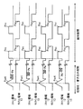
図13は、従来のサステインドライバの構成を示す回路図である。図13に示すように、サステインドライバ400は、回収コンデンサC11、回収コイルL11、スイッチSW11,SW12,SW21,SW22およびダイオードD11,D12を含む。
【0004】
スイッチSW11は、電源端子V4とノードN11との間に接続され、スイッチSW12は、ノードN11と接地端子との間に接続されている。電源端子V4には、電圧Vsusが印加される。ノードN11は、例えば480本のサステイン電極に接続され、図13では、複数のサステイン電極と接地端子との間の全容量に相当するパネル容量Cpが示されている。
【0005】
回収コンデンサC11は、ノードN13と接地端子との間に接続されている。ノードN13とノードN12との間にスイッチSW21およびダイオードD11が直列に接続され、ノードN12とノードN13との間にダイオードD12およびスイッチSW22が直列に接続されている。回収コイルL11は、ノードN12とノードN11との間に接続されている。
【0006】
図14は、図13のサステインドライバ400の維持期間の動作を示すタイミング図である。図14には、図13のノードN11の電圧およびスイッチSW21,SW11,SW22,SW12の動作が示される。
【0007】
まず、期間Taにおいて、スイッチSW21がオンし、スイッチSW12がオフする。このとき、スイッチSW11,SW22はオフしている。これにより、回収コイルL11およびパネル容量CpによるLC共振により、ノードN11の電圧が緩やかに上昇する。次に、期間Tbにおいて、スイッチSW21がオフし、スイッチSW11がオンする。これにより、ノードN11の電圧が急激に上昇し、期間TcではノードN11の電圧がVsusに固定される。
【0008】
次に、期間Tdでは、スイッチSW11がオフし、スイッチSW22がオンする。これにより、回収コイルL11およびパネル容量CpによるLC共振により、ノードN11の電圧が緩やかに降下する。その後、期間Teにおいて、スイッチSW22がオフし、スイッチSW12がオンする。これにより、ノードN11の電圧が急激に降下し、接地電位に固定される。上記の動作を維持期間において繰り返し行うことにより、複数のサステイン電極に周期的な維持パルスPsuが印加される。
【0009】
上記のように、維持パルスPsuの立ち上がり部分および立ち下がり部分は、スイッチSW21またはスイッチSW22の動作による期間Ta,TdのLC共振部とスイッチSW11またはスイッチSW12のオン動作による期間Tb,Teのエッジ部e1,e2とで構成されている。
【0010】
【発明が解決しようとする課題】
上記のスイッチSW11,SW12,SW21,SW22は、通常、スイッチング素子であるFET(電界効果型トランジスタ)により構成され、各FETは寄生容量としてドレイン・ソース間に容量を有し、各FETに接続される配線は、インダクタンス成分を有している。このため、スイッチSW11等がオフからオンへ変化するときに、ドレイン・ソース間の容量と配線のインダクタンス成分とによりLC共振が発生し、このLC共振により不要な電磁波が輻射される。
【0011】
また、上記の各ダイオードD11,D12も、寄生容量としてアノード・カソード間に容量を有し、各ダイオードに接続される配線も、インダクタンス成分を有している。このため、スイッチSW11等がオフからオンへ変化するときに、アノード・カソード間の容量と配線のインダクタンス成分とによりLC共振が発生し、このLC共振により不要な電磁波が輻射される。
【0012】
さらに、各FETのドレイン・ソース間の容量および各ダイオードのアノード・カソード間の容量と各配線のインダクタンス成分とが小さいため、LC共振の共振周波数が高くなり、発生する電磁波の周波数も高くなる。一方、電気用品取締法による不要輻射の規格では、30MHz以上の高周波の電磁波に対する限度値が定められている。したがって、このような高周波の電磁波の輻射は、他の電子機器に電磁的な悪影響を及ぼす恐れがあるため、この不要な高周波の電磁波の輻射を抑制することが望まれる。
【0013】
本発明の目的は、不要な高周波の電磁波の輻射を抑制することができる駆動回路を用いたプラズマディスプレイ装置を提供することである。
【0014】
【課題を解決するための手段】
(1)第1の発明
第1の発明に係るプラズマディスプレイ装置は、プラズマディスプレイパネルの容量性負荷に電荷を供給する回収コンデンサと、第1の電圧源に接続される第1のスイッチング手段と、第1のスイッチング手段とプラズマディスプレイとの間に接続される配線手段と、第1のスイッチング手段に並列に接続され、第1の電圧源と配線手段とを接続する第1の容量性素子と、第2の電圧源と配線手段とに接続される第2のスイッチング手段と、第2のスイッチング手段に並列に接続され、第2の電圧源と配線手段とを接続する第2の容量性素子と、回収コンデンサに接続される第3のスイッチング手段と、第3のスイッチング手段と配線手段との間に接続されるインダクタンス素子とを備え、第3のスイッチング手段をオンすることにより、配線手段の電位が上昇してピーク電圧から下がり始めた後に、第1のスイッチング手段をオンすることにより、配線手段の電位を第1の電圧源の電位とする構成としたものである。
【0015】
本発明に係るプラズマディスプレイ装置においては、インダクタンス素子と容量性負荷とのLC共振により駆動パルスを立ち上げまたは立ち下げることができるとともに、第1のスイッチング手段および配線手段を介してプラズマディスプレイパネルの容量性負荷に第1の電圧源の電位を供給することにより駆動パルスを立ち上げ、第2のスイッチング手段および配線手段を介してプラズマディスプレイパネルの容量性負荷に第2の電圧源の電位を供給することにより駆動パルスを立ち下げることができる。また、回収コンデンサにより容量性負荷から電荷を回収することができるので、駆動回路の消費電力を低減することができる。
【0016】
また、第1のスイッチング手段に第1の容量性素子が接続され、第2のスイッチング手段に第2の容量性素子が接続されている。それにより、LC共振経路における容量が大きくなり、第1および第2のスイッチング手段および配線手段によるLC共振の共振周波数を低減することができるので、不要な高周波の電磁波の輻射を抑制することができる。
【0017】
(2)第2の発明
第2の発明に係るプラズマディスプレイ装置は、プラズマディスプレイパネルの容量性負荷に電荷を供給する回収コンデンサと、第1の電圧源に接続される第1のスイッチング手段と、第1のスイッチング手段とプラズマディスプレイとの間に接続される配線手段と、第2の電圧源と配線手段とに接続される第2のスイッチング手段と、回収コンデンサに接続される第3のスイッチング手段と、第3のスイッチング手段と配線手段との間に接続されるインダクタンス素子と、第3のスイッチング手段に並列に接続され、回収コンデンサとインダクタンス素子とを接続する容量性素子とを備え、第3のスイッチング手段をオンすることにより、配線手段の電位が上昇してピーク電圧から下がり始めた後に、第1のスイッチング手段をオンすることにより、配線手段の電位を第1の電圧源の電位とする構成としたものである。
【0018】
本発明に係るプラズマディスプレイ装置においては、インダクタンス素子と容量性負荷とのLC共振により駆動パルスを立ち上げまたは立ち下げることができるとともに、第1のスイッチング手段および配線手段を介してプラズマディスプレイパネルの容量性負荷に第1の電圧源の電位を供給することにより駆動パルスを立ち上げ、第2のスイッチング手段および配線手段を介してプラズマディスプレイパネルの容量性負荷に第2の電圧源の電位を供給することにより駆動パルスを立ち下げることができる。また、回収コンデンサにより容量性負荷から電荷を回収することができるので、駆動回路の消費電力を低減することができる。
【0019】
また、第3のスイッチング手段に容量性素子が接続されている。それにより、LC共振経路における容量が大きくなり、第1および第2のスイッチング手段および配線手段によるLC共振の共振周波数を低減することができるので、不要な高周波の電磁波の輻射を抑制することができる。
【0044】
【発明の実施の形態】
以下、本発明による駆動回路の一例として、プラズマディスプレイ装置に用いられるサステインドライバについて説明する。なお、本発明の駆動回路は、容量性負荷を駆動するものであれば、他の装置にも同様に適用することができ、たとえば、プラズマディスプレイパネル、液晶ディスプレイ、エレクトロルミネッセンスディスプレイ等の表示装置の駆動回路に適用できる。また、本発明の駆動回路をプラズマディスプレイパネルに用いる場合は、AC型、DC型等のいずれのプラズマディスプレイパネルの駆動回路にも適用でき、アドレス電極、サステイン電極およびスキャン電極のいずれの駆動回路にも適用できるが、サステイン電極およびスキャン電極の駆動回路に好適に用いることができる。
【0045】
図1は、本発明の第1の実施の形態によるサステインドライバを用いたプラズマディスプレイ装置の構成を示すブロック図である。
【0046】
図1のプラズマディスプレイ装置は、PDP(プラズマディスプレイパネル)1、データドライバ2、スキャンドライバ3、複数のスキャンドライバIC(回路)3aおよびサステインドライバ4を含む。
【0047】
PDP1は、複数のアドレス電極(データ電極)11、複数のスキャン電極(走査電極)12および複数のサステイン電極(維持電極)13を含む。複数のアドレス電極11は、画面の垂直方向に配列され、複数のスキャン電極12および複数のサステイン電極13は、画面の水平方向に配列されている。また、複数のサステイン電極13は、共通に接続されている。アドレス電極11、スキャン電極12およびサステイン電極13の各交点には、放電セルが形成され、各放電セルが画面上の画素を構成する。
【0048】
データドライバ2は、PDP1の複数のアドレス電極11に接続されている。複数のスキャンドライバIC3aは、スキャンドライバ3に接続されている。各スキャンドライバIC3aには、PDP1の複数のスキャン電極12が接続されている。サステインドライバ4は、PDP1の複数のサステイン電極13に接続されている。
【0049】
データドライバ2は、書き込み期間において、画像データに応じてPDP1の該当するアドレス電極11に書き込みパルスを印加する。複数のスキャンドライバIC3aは、スキャンドライバ3により駆動され、書き込み期間において、シフトパルスSHを垂直走査方向にシフトしつつPDP1の複数のスキャン電極12に書き込みパルスを順に印加する。これにより、該当する放電セルにおいてアドレス放電が行われる。
【0050】
また、複数のスキャンドライバIC3aは、維持期間において、周期的な維持パルスをPDP1の複数のスキャン電極12に印加する。一方、サステインドライバ4は、維持期間において、PDP1の複数のサステイン電極13にスキャン電極12の維持パルスに対して180°位相のずれた維持パルスを同時に印加する。これにより、該当する放電セルにおいて維持放電が行われる。
【0051】
図2は、図1のPDP1におけるスキャン電極12およびサステイン電極13の駆動電圧の一例を示すタイミング図である。
【0052】
初期化および書き込み期間には、複数のスキャン電極12に初期化パルス(セットアップパルス)Psetが同時に印加される。その後、複数のスキャン電極12に書き込みパルスPwが順に印加される。これにより、PDP1の該当する放電セルにおいてアドレス放電が起こる。
【0053】
次に、維持期間において、複数のスキャン電極12に維持パルスPscが周期的に印加され、複数のサステイン電極13に維持パルスPsuが周期的に印加される。維持パルスPsuの位相は、維持パルスPscの位相に対して180°ずれている。これにより、アドレス放電に続いて維持放電が起こる。
【0054】
次に、図1に示すサステインドライバ4について説明する。図3は、図1に示すサステインドライバ4の構成を示す回路図である。
【0055】
図3のサステインドライバ4は、スイッチング素子であるnチャネル型のFET(電界効果型トランジスタ、以下トランジスタと称す)Q1〜Q4、コンデンサC1,C2、回収コンデンサCr、回収コイルLおよびダイオードD1,D2を含む。
【0056】
トランジスタQ1は、一端が電源端子V1に接続され、他端が配線L1を介してノードN1に接続され、ゲートには制御信号S1が入力される。トランジスタQ1は、寄生容量としてドレイン・ソース間の容量CP1を有し、トランジスタQ1のドレイン・ソース間には、コンデンサC1が並列に接続される。電源端子V1には、電圧Vsusが印加される。
【0057】
トランジスタQ2は、一端が配線L2を介してノードN1に接続され、他端が接地端子に接続され、ゲートには制御信号S2が入力される。トランジスタQ2は、寄生容量としてドレイン・ソース間の容量CP2を有し、トランジスタQ2のドレイン・ソース間には、コンデンサC2が並列に接続される。
【0058】
ノードN1は、例えば480本のサステイン電極13に接続されているが、図3では、複数のサステイン電極13と接地端子との間の全容量に相当するパネル容量Cpが示されている。
【0059】
回収コンデンサCrは、ノードN3と接地端子との間に接続されている。トランジスタQ3およびダイオードD1は、ノードN3とノードN2との間に直列に接続されている。ダイオードD2およびトランジスタQ4は、ノードN2とノードN3との間に直列に接続されている。トランジスタQ3のゲートには、制御信号S3が入力され、トランジスタQ4のゲートには制御信号S4が入力される。回収コイルLはノードN2とノードN1との間に接続されている。
【0060】
本実施の形態では、トランジスタQ1,Q2が電気素子、スイッチング手段および維持パルス用スイッチング手段に相当し、配線L1,L2が配線手段に相当し、コンデンサC1,C2が周波数低減手段に相当し、電源端子V1および接地端子が電圧源に相当する。また、トランジスタQ1が第1のスイッチング手段に相当し、トランジスタQ2が第2のスイッチング手段に相当し、配線L1が第1の配線手段に相当し、配線L2が第2の配線手段に相当し、コンデンサC1が第1の容量性素子に相当し、コンデンサC2が第2の容量性素子に相当し、電源端子V1が第1の電圧源に相当し、接地端子が第2の電圧源に相当する。
【0061】
次に、上記のように構成されたサステインドライバ4の維持期間の動作について説明する。
【0062】
まず、制御信号S2がローレベルになりトランジスタQ2がオフし、制御信号S3がハイレベルになりトランジスタQ3がオンする。このとき、制御信号S1はローレベルにありトランジスタQ1はオフし、制御信号S4はローレベルにありトランジスタQ4はオフしている。したがって、回収コンデンサCrがトランジスタQ3およびダイオードD1を介して回収コイルLに接続され、回収コイルLおよびパネル容量CpによるLC共振によりノードN1の電圧が滑らかに上昇する。このとき、回収コンデンサCrの電荷がトランジスタQ3、ダイオードD1および回収コイルLを介してパネル容量Cpへ放出される。
【0063】
また、このとき、トランジスタQ3、ダイオードD1および回収コイルLを介して流れる電流は、パネル容量Cpに流入するだけでなく、配線L1を介してトランジスタQ1のドレイン・ソース間の容量CP1およびコンデンサC1を流れるとともに、配線L2を介してトランジスタQ2のドレイン・ソース間の容量CP2およびコンデンサC2にも流れる。このため、配線L1,L2の各インダクタンス成分とトランジスタQ1,Q2の各ドレイン・ソース間の容量CP1,CP2およびコンデンサC1,C2によりLC共振が発生する。
【0064】
しかしながら、本実施の形態では、このLC共振に寄与する容量は、ドレイン・ソース間の容量CP1,CP2とコンデンサC1,C2とをそれぞれ加算した容量となるため、その共振周波数はドレイン・ソース間の容量CP1,CP2のみによる共振周波数よりも低減される。具体的には、LC共振の共振周波数が30MHz未満になるように、各コンデンサC1,C2の容量を各トランジスタQ1,Q2のドレイン・ソース間の容量CP1,CP2に対して、例えば約5〜10倍に設定している。
【0065】
ここで、一例として、2000pFのコンデンサをFETのドレイン・ソース間に並列に接続した場合のドレイン・ソース間の容量とドレイン・ソース間の電圧との関係について説明する。図4は、2000pFのコンデンサをFETに並列に接続した場合と接続しない場合のドレイン・ソース間の容量Cds(pF)とドレイン・ソース間の電圧Vds(V)との関係を示す図である。図4では、FETのドレイン・ソース間にコンデンサを接続していない場合を破線で示し、2000pFのコンデンサを並列に接続した場合を実線で示している。
【0066】
図4に示すように、2000pFのコンデンサがFETのドレイン・ソース間に並列に接続されると、接続しない場合に比べてドレイン・ソース間の容量Cdsが増加することがわかる。本実施の形態の場合、図3に示すトランジスタQ1,Q2のドレイン・ソース間の電圧Vdsが約200Vであるので、2000pFのコンデンサを各トランジスタQ1,Q2のドレイン・ソース間に並列に接続することにより、各トランジスタQ1,Q2のドレイン・ソース間の容量Cdsがコンデンサを接続しない場合に対して約10倍程度増加することがわかる。
【0067】
上記のように、トランジスタQ1,Q2のドレイン・ソース間にコンデンサC1,C2を並列に接続することにより、トランジスタQ3がオフからオンへ変化したときに発生する、配線L1,L2のインダクタンス成分とトランジスタQ1,Q2のドレイン・ソース間の容量CP1,CP2およびコンデンサC1,C2とによるLC共振の共振周波数が30MHz未満となり、30MHz以上の不要な電磁波の輻射が抑制される。
【0068】
次に、制御信号S1がハイレベルになりトランジスタQ1がオンし、制御信号S3がローレベルになりトランジスタQ3がオフする。したがって、ノードN1が電源端子V1に接続され、ノードN1の電圧が急激に上昇し、電圧Vsusに固定される。
【0069】
このとき、電源端子V1からトランジスタQ1を介して流れる電流は、パネル容量Cpに流入するだけでなく、配線L1,L2を介してトランジスタQ2のドレイン・ソース間の容量CP2およびコンデンサC2にも流入する。このため、配線L1,L2のインダクタンス成分とトランジスタQ2のドレイン・ソース間の容量CP2およびコンデンサC2によりLC共振が発生する。
【0070】
この場合も、上記と同様に、このLC共振に寄与する容量がドレイン・ソース間の容量CP2とコンデンサC2とを加算した容量となるので、トランジスタQ1がオフからオンへ変化したときに発生する、配線L1,L2のインダクタンス成分とトランジスタQ2のドレイン・ソース間の容量CP2およびコンデンサC2によるLC共振の共振周波数が30MHz未満となり、30MHz以上の不要な電磁波の輻射が抑制される。
【0071】
次に、制御信号S1がローレベルになりトランジスタQ1がオフし、制御信号S4がハイレベルになりトランジスタQ4がオンする。したがって、回収コンデンサCrがダイオードD2およびトランジスタQ4を介して回収コイルLに接続され、回収コイルLおよびパネル容量CpによるLC共振によりノードN1の電圧が緩やかに降下する。このとき、パネル容量Cpに蓄えられた電荷は、回収コイルL、ダイオードD2およびトランジスタQ4を介して回収コンデンサCrに蓄えられ、電荷の回収が行われる。
【0072】
また、このとき、パネル容量Cpから流れる電流は、回収コイルL、ダイオードD2およびトランジスタQ4を介して回収コンデンサCrへ流入するだけでなく、配線L1,L2を介してトランジスタQ1,Q2のドレイン・ソース間の容量CP1,CP2およびコンデンサC1,C2へも流れる。このため、配線L1,L2のインダクタンス成分とトランジスタQ1,Q2のドレイン・ソース間の容量CP1,CP2およびコンデンサC1,C2によりLC共振が発生する。
【0073】
この場合も、上記と同様に、このLC共振に寄与する容量がドレイン・ソース間の容量CP1,CP2とコンデンサC1,C2とをそれぞれ加算した容量となるので、トランジスタQ4がオフからオンへ変化したときに発生する、配線L1,L2のインダクタンス成分とトランジスタQ1,Q2のドレイン・ソース間の容量CP1,CP2およびコンデンサC1,C2によるLC共振の共振周波数が30MHz未満となり、30MHz以上の不要な電磁波の輻射が抑制される。
【0074】
次に、制御信号S2がハイレベルになりトランジスタQ2がオンし、制御信号S4がローレベルになりトランジスタQ4がオフする。したがって、ノードN1が接地端子に接続され、ノードN1の電圧が急激に降下し、接地電位に固定される。
【0075】
このとき、トランジスタQ2を介して接地端子へ流れる電流は、パネル容量Cpから流入するだけでなく、配線L1,L2を介してトランジスタQ1のドレイン・ソース間の容量CP1およびコンデンサC1からも流入する。このため、配線L1,L2のインダクタンス成分とトランジスタQ1のドレイン・ソース間の容量CP1およびコンデンサC1によりLC共振が発生する。
【0076】
この場合も、上記と同様に、このLC共振に寄与する容量がドレイン・ソース間の容量CP1とコンデンサC1とを加算した容量となるので、トランジスタQ2がオフからオンへ変化したときに発生する、配線L1,L2のインダクタンス成分とトランジスタQ1のドレイン・ソース間の容量CP1およびコンデンサC1によるLC共振の共振周波数も、30MHz未満となり、30MHz以上の不要な電磁波の輻射が抑制される。
【0077】
上記の動作を維持期間において繰り返し行うことにより、図14に示す従来の維持パルスPsuと同様の波形を有する維持パルスPsuが複数のサステイン電極13に周期的に印加されるとともに、30MHz以上の不要な電磁波の輻射が抑制される。
【0078】
次に、上記のようにトランジスタQ1,Q2にコンデンサC1,C2を並列に接続した場合の電磁波の輻射レベルの低減効果について説明する。図5は、図1に示すプラズマディスプレイ装置から放出される電磁波の輻射レベルと周波数との関係を示す図である。図5では、コンデンサC1,C2をトランジスタQ1,Q2のドレイン・ソース間に並列に接続した場合を実線で示し、コンデンサC1,C2を接続していない場合を破線で示す。
【0079】
図5に示すように、コンデンサC1,C2を接続していない場合、電磁波の輻射レベルは30MHzより高い周波数f0でピークを取り、30MHz以上の電磁波の輻射レベルが高くなっていることがわかる。一方、コンデンサC1,C2をトランジスタQ1,Q2のドレイン・ソース間に並列に接続した場合、共振周波数がf0からf1へ低減され、30MHzより低い周波数f1でピークを取るようになる。したがって、30MHz以上の電磁波の輻射レベルが十分に低減され、30MHz以上の不要な電磁波の輻射を十分に抑制できることがわかる。
【0080】
上記のように、本実施の形態では、コンデンサC1,C2がトランジスタQ1,Q2のドレイン・ソース間に並列に接続されているので、トランジスタQ1〜Q4がオフからオンへ変化したときに発生するLC共振の共振周波数を30MHz未満の低い周波数へ移動させることができる。したがって、30MHz以上の高周波の電磁波の輻射を抑制することができる。
【0081】
次に、図1に示すサステインドライバ4として用いられる他のサステインドライバについて説明する。図6は、本発明の第2の実施の形態によるサステインドライバの構成を示す回路図である。
【0082】
図6に示すサステインドライバ4aと図3に示すサステインドライバ4とで異なる点は、コンデンサC1,C2が省略され、トランジスタQ3,Q4に並列に接続されるコンデンサC3,C4が付加された点であり、その他の点は図3に示すサステインドライバ4と同様であるので、同一部分には同一符号を付し、以下詳細な説明を省略する。
【0083】
図6に示すように、コンデンサC3は、トランジスタQ3のドレイン・ソース間に並列に接続され、コンデンサC4は、トランジスタQ4のドレイン・ソース間に並列に接続される。トランジスタQ3の一端は、配線L3を介してノードN3に接続され、トランジスタQ4の一端は、配線L4を介してノードN3に接続されている。なお、配線L3および配線L4は、トランジスタQ3およびトランジスタQ4のドレイン・ソース間の配線全体を指している。トランジスタQ3は、寄生容量としてドレイン・ソース間の容量CP3を有し、トランジスタQ4は、寄生容量としてドレイン・ソース間の容量CP4を有する。ダイオードD1は、寄生容量としてアノード・カソード間の容量CP5を有し、ダイオードD2は、寄生容量としてアノード・カソード間の容量CP6を有する。
【0084】
本実施の形態では、トランジスタQ3,Q4が電気素子、スイッチング手段および維持パルス用スイッチング手段に相当し、配線L3,L4が配線手段に相当し、コンデンサC3,C4が周波数低減手段に相当し、回収コイルLがインダクタンス素子に相当し、回収コンデンサCrが回収用容量性素子に相当し、ダイオードD1,D2が一方向性導通素子、トランジスタQ3,Q4がスイッチング素子に相当する。
【0085】
次に、上記のように構成されたサステインドライバ4aの維持期間の動作について説明する。図7は、図6に示すサステインドライバ4aの維持期間の動作を説明するためのタイミング図である。図7には、トランジスタQ1〜Q4に入力される制御信号S1〜S4およびノードN1〜N3の各電圧が示される。なお、図6に示すサステインドライバ4aの基本的な動作は、図3に示すサステインドライバ4と同様であるので、LC共振の発生メカニズム等の異なる点についてのみ以下詳細に説明する。
【0086】
まず、トランジスタQ4のドレイン・ソース間の容量CP4および配線L4のインダクタンス成分によるLC共振は、トランジスタQ4がオフ状態にあり、かつ、トランジスタQ4のドレイン・ソース間に急激な電圧変化が生じる場合に発生する。具体的には、図7に示す時刻t1,t2においてドレイン・ソース間の容量CP4および配線L4のインダクタンス成分によるLC共振が発生する。
【0087】
時刻t1の場合、制御信号S3がハイレベルになりトランジスタQ3がオンし、ノードN2の電位が0VからノードN3の電位約Vsus/2に立ち上がる瞬間に、LC共振が発生する。このとき、ダイオードD2のアノード・カソード間の容量CP6、トランジスタQ4のドレイン・ソース間の容量CP4および配線L4を介して高周波の電流がノードN2からノードN3に向かって流れようとする。このため、トランジスタQ4のドレイン・ソース間の容量CP4および配線L4のインダクタンス成分により高周波のLC共振が発生し、高周波の電磁波として輻射される。
【0088】
また、時刻t2の場合、ノードN1の電位が回収コイルLおよびパネル容量CpによるLC共振によりピーク電圧から下がり始め、回収コイルLに流れる電流の方向がノードN1からノードN2へと逆転すると、ダイオードD1が非導通となるために、電流は経路を断たれ、ノードN2の電位は、急激にノードN1の電位に向かって上昇する。このとき、ダイオードD1のアノード・カソード間の容量CP5等のノードN2に接続されている浮遊容量および回収コイルLによるLC共振を発生し、ノードN2の電位がリンギングしながら上昇する瞬間に、高周波のLC共振が発生する。
【0089】
このとき、ダイオードD2はオンし、トランジスタQ4のドレイン・ソース間の容量CP4および配線L4を介して高周波の電流がノードN2からノードN3に向かって流れようとする。このため、トランジスタQ4のドレイン・ソース間の容量CP4および配線L4のインダクタンス成分により高周波のLC共振が発生し、高周波の電磁波として輻射される。
【0090】
しかしながら、本実施の形態では、トランジスタQ4に並列にコンデンサC4が接続されているため、トランジスタQ4のドレイン・ソース間の容量CP4および配線L4のインダクタンス成分によるLC共振に寄与する容量は、トランジスタQ4のドレイン・ソース間の容量CP4とコンデンサC4とを加算した容量となるため、その共振周波数はドレイン・ソース間の容量CP4のみによる共振周波数よりも低減される。具体的には、このLC共振の共振周波数が30MHz未満になるように、コンデンサC4の容量が設定され、30MHz以上の不要の電磁波の輻射を抑制している。
【0091】
次に、トランジスタQ3のドレイン・ソース間の容量CP3および配線L3のインダクタンス成分によるLC共振は、トランジスタQ3がオフ状態にあり、かつ、トランジスタQ3のドレイン・ソース間に急激な電圧変化が生じる場合に発生する。具体的には、図7に示す時刻t3,t4においてドレイン・ソース間の容量CP3および配線L3のインダクタンス成分によるLC共振が発生する。
【0092】
時刻t3の場合、維持パルスPsuの立ち上がり時の電力回収期間が終了して制御信号S1がハイレベルになりトランジスタQ1がオンし、電源端子V1の電圧VsusがノードN2に印加されている状態から、制御信号S4がハイレベルになりトランジスタQ4がオンし、ノードN2の電位がVsusからノードN3の電位約Vsus/2に立ち下がる瞬間に、LC共振が発生する。
【0093】
このとき、配線L3、トランジスタQ3のドレイン・ソース間の容量CP3およびダイオードD1のアノード・カソード間の容量CP5を介して高周波の電流がノードN3からノードN2に向かって流れようとする。このため、トランジスタQ3のドレイン・ソース間の容量CP3および配線L3のインダクタンス成分により高周波のLC共振が発生し、高周波の電磁波として輻射される。
【0094】
また、時刻t4の場合、維持パルスPsuの立ち下がり時の電力回収期間が終了し、回収コイルLに流れる電流の方向がノードN2からノードN1へと逆転すると、ダイオードD2が非導通となるために、電流は経路を断たれ、ノードN2の電位は、急激にノードN1の電位に向かって降下する。このとき、ダイオードD2のアノード・カソード間の容量CP6等のノードN2に接続されている浮遊容量および回収コイルLによるLC共振を発生し、ノードN2の電位がリンギングしながら下降する瞬間に、高周波のLC共振が発生する。
【0095】
このとき、ダイオードD1はオンし、配線L3およびトランジスタQ3のドレイン・ソース間の容量CP3を介して高周波の電流がノードN3からノードN2に向かって流れようとする。このため、トランジスタQ3のドレイン・ソース間の容量CP3および配線L3のインダクタンス成分により高周波のLC共振が発生し、高周波の電磁波として輻射される。
【0096】
しかしながら、本実施の形態では、トランジスタQ3に並列にコンデンサC3が接続されているため、トランジスタQ3のドレイン・ソース間の容量CP3および配線L3のインダクタンス成分によるLC共振に寄与する容量は、トランジスタQ3のドレイン・ソース間の容量CP3とコンデンサC3とを加算した容量となるため、その共振周波数はドレイン・ソース間の容量CP3のみによる共振周波数よりも低減される。具体的には、このLC共振の共振周波数が30MHz未満になるように、コンデンサC3の容量が設定され、30MHz以上の不要の電磁波の輻射を抑制している。
【0097】
上記のように、本実施の形態でも、コンデンサC3,C4がトランジスタQ3,Q4のドレイン・ソース間に並列に接続されているので、配線L3,L4のインダクタンス成分とトランジスタQ3,Q4のドレイン・ソース間の容量CP3,CP4により発生するLC共振の共振周波数を30MHz未満の低い周波数に移動させることができる。したがって、30MHz以上の高周波の電磁波の輻射を抑制することができる。
【0098】
図8は、本発明の第3の実施の形態によるサステインドライバの構成を示す回路図である。
【0099】
図8に示すサステインドライバ4bと図3に示すサステインドライバ4とで異なる点は、コンデンサC1,C2が省略され、ダイオードD1,D2に並列に接続されるコンデンサC5,C6が付加された点であり、その他の点は図3に示すサステインドライバ4と同様であるので、同一部分には同一符号を付し、以下詳細な説明を省略する。
【0100】
図8に示すように、コンデンサC5は、ダイオードD1のアノード・カソード間に並列に接続され、コンデンサC6は、ダイオードD2のアノード・カソード間に並列に接続される。ダイオードD1のカソードは、配線L5を介してノードN2に接続され、ダイオードD2のアノードは、配線L6を介してノードN2に接続されている。ダイオードD1は、寄生容量としてアノード・カソード間の容量CP5を有し、ダイオードD2は、寄生容量としてアノード・カソード間の容量CP6を有する。なお、トランジスタQ3,Q4も第2の実施の形態と同様に寄生容量CP3,CP4を有している。
【0101】
本実施の形態では、ダイオードD1,D2が電気素子、スイッチング手段および維持パルス用スイッチング手段に相当し、配線L5,L6が配線手段に相当し、コンデンサC5,C6が周波数低減手段に相当し、回収コイルLがインダクタンス素子に相当し、回収コンデンサCrが回収用容量性素子に相当し、ダイオードD1,D2が一方向性導通素子、トランジスタQ3,Q4がスイッチング素子に相当する。
【0102】
次に、上記のように構成されたサステインドライバ4bの維持期間の動作について説明する。なお、図8に示すサステインドライバ4bの基本的な動作は、図3および図6に示すサステインドライバ4,4aと同様であるので、LC共振の発生メカニズム等の異なる点についてのみ以下詳細に説明する。
【0103】
まず、ダイオードD1のアノード・カソード間の容量CP5および配線L5のインダクタンス成分によるLC共振は、ダイオードD1がオフ状態にあり、かつ、ダイオードD1のアノード・カソード間に急激な電圧変化が生じる場合に発生する。具体的には、図7に示す時刻t2,t3においてアノード・カソード間の容量CP5および配線L5のインダクタンス成分によるLC共振が発生する。
【0104】
時刻t2の場合、制御信号S3がハイレベルになりトランジスタQ3がオンし、ノードN2の電位がノードN3の電位約Vsus/2と同じ電位になっている状態から、ノードN1の電位が回収コイルLおよびパネル容量CpによるLC共振によりピーク電圧から下がり始め、回収コイルLに流れる電流の方向がノードN1からノードN2へと逆転すると、ダイオードD1が非導通となるために、電流は経路を断たれ、ノードN2の電位は、急激にノードN1の電位に向かって上昇する。このとき、ダイオードD1のアノード・カソード間の容量CP5等のノードN2に接続されている浮遊容量および回収コイルLによるLC共振を発生し、ノードN2の電位がリンギングしながら上昇する瞬間に、高周波のLC共振が発生する。
【0105】
このとき、ダイオードD1は逆バイアスの状態にありオフされているが、トランジスタQ3はオンしているため、配線L5およびダイオードD1のアノード・カソード間の容量CP5を介して高周波の電流がノードN2からノードN3に向かって流れようとする。このため、ダイオードD1のアノード・カソード間の容量CP5および配線L5のインダクタンス成分により高周波のLC共振が発生し、高周波の電磁波として輻射される。
【0106】
また、時刻t3の場合、維持パルスPsuの立ち上がり時の電力回収期間が終了して制御信号S1がハイレベルになりトランジスタQ1がオンし、電源端子V1の電圧VsusがノードN2に印加されている状態から、制御信号S4がハイレベルになりトランジスタQ4がオンし、ノードN2の電位がVsusからノードN3の電位約Vsus/2に立ち下がる瞬間に、LC共振が発生する。
【0107】
このとき、トランジスタQ3のドレイン・ソース間の容量CP3、ダイオードD1のアノード・カソード間の容量CP5および配線L5を介して高周波の電流がノードN3からノードN2に向かって流れようとする。このため、ダイオードD1のアノード・カソード間の容量CP5および配線L5のインダクタンス成分により高周波のLC共振が発生し、高周波の電磁波として輻射される。
【0108】
しかしながら、本実施の形態では、ダイオードD1に並列にコンデンサC5が接続されているため、ダイオードD1のアノード・カソード間の容量CP5および配線L5のインダクタンス成分によるLC共振に寄与する容量は、ダイオードD1のアノード・カソード間の容量CP5とコンデンサC5とを加算した容量となるため、その共振周波数はアノード・カソード間の容量CP5のみによる共振周波数よりも低減される。具体的には、このLC共振の共振周波数が30MHz未満になるように、コンデンサC5の容量が設定され、30MHz以上の不要の電磁波の輻射を抑制している。
【0109】
次に、ダイオードD2のアノード・カソード間の容量CP6および配線L6のインダクタンス成分によるLC共振は、ダイオードD2がオフ状態にあり、かつ、ダイオードD2のアノード・カソード間に急激な電圧変化が生じる場合に発生する。具体的には、図7に示す時刻t1,t4においてアノード・カソード間の容量CP6および配線L6のインダクタンス成分によるLC共振が発生する。
【0110】
時刻t1の場合、制御信号S3がハイレベルになりトランジスタQ3がオンし、ノードN2の電位が0VからノードN3の電位約Vsus/2に立ち上がる瞬間に、LC共振が発生する。このとき、配線L6、ダイオードD2のアノード・カソード間の容量CP6およびトランジスタQ4のドレイン・ソース間の容量CP4を介して高周波の電流がノードN2からノードN3に向かって流れようとする。このため、ダイオードD2のアノード・カソード間の容量CP6および配線L6のインダクタンス成分により高周波のLC共振が発生し、高周波の電磁波として輻射される。
【0111】
また、時刻t4の場合、維持パルスPsuの立ち下がり時の電力回収期間が終了し、回収コイルLに流れる電流の方向がノードN2からノードN1へと逆転すると、ダイオードD2が非導通となるために、電流は経路を断たれ、ノードN2の電位は、急激にノードN1の電位に向かって降下する。このとき、ダイオードD2のアノード・カソード間の容量CP6等のノードN2に接続されている浮遊容量および回収コイルLによるLC共振を発生し、ノードN2の電位がリンギングしながら下降する瞬間に、高周波のLC共振が発生する。
【0112】
このとき、ダイオードD2は逆バイアスの状態にありオフされているが、トランジスタQ4はオンしているため、ダイオードD2のアノード・カソード間の容量CP6および配線L6を介して高周波の電流がノードN3からノードN2に向かって流れようとする。このため、ダイオードD2のアノード・カソード間の容量CP6および配線L6のインダクタンス成分により高周波のLC共振が発生し、高周波の電磁波として輻射される。
【0113】
しかしながら、本実施の形態では、ダイオードD2に並列にコンデンサC6が接続されているため、ダイオードD2のアノード・カソード間の容量CP6および配線L6のインダクタンス成分によるLC共振に寄与する容量は、ダイオードD2のアノード・カソード間の容量CP6とコンデンサC6とを加算した容量となるため、その共振周波数はアノード・カソード間の容量CP6のみによる共振周波数よりも低減される。具体的には、このLC共振の共振周波数が30MHz未満になるように、コンデンサC6の容量が設定され、30MHz以上の不要の電磁波の輻射を抑制している。
【0114】
上記のように、本実施の形態でも、コンデンサC5,C6がダイオードD1,D2のアノード・カソード間に並列に接続されているので、配線L5,L6のインダクタンス成分とダイオードD1,D2のアノード・カソード間の容量CP5,CP6により発生するLC共振の共振周波数を30MHz未満の低い周波数に移動させることができる。したがって、30MHz以上の高周波の電磁波の輻射を抑制することができる。
【0115】
図9は、本発明の第4の実施の形態によるサステインドライバの構成を示す回路図である。
【0116】
図9に示すサステインドライバ4cと図3に示すサステインドライバ4とで異なる点は、コンデンサC1,C2が省略され、電源端子V1とノードN2との間にダイオードD3およびコンデンサC7が付加され、ノードN2と接地端子との間にダイオードD4およびコンデンサC8が付加された点であり、その他の点は図3に示すサステインドライバ4と同様であるので、同一部分には同一符号を付し、以下詳細な説明を省略する。
【0117】
図9に示すように、ダイオードD3は、カソードが電源端子V1に接続され、アノードが配線L7を介してノードN2に接続される。ダイオードD3は、寄生容量としてアノード・カソード間の容量CP7を有し、ダイオードD3のアノード・カソード間には、コンデンサC7が並列に接続される。
【0118】
また、ダイオードD4は、カソードが配線L8を介してノードN2に接続され、アノードが接地端子に接続される。ダイオードD4は、寄生容量としてアノード・カソード間の容量CP8を有し、ダイオードD4のアノード・カソード間には、コンデンサC8が並列に接続される。
【0119】
ダイオードD3,D4は、電流クリップの目的で付加したものであり、トランジスタQ3,Q4の耐圧が低い場合に、トランジスタQ3,Q4に耐圧以上の電圧がかからないように保護している。したがって、ダイオードD3は、通常オフ状態にあり、ノードN2の電位がVsusを超えるときにのみオンし、ダイオードD4は、通常オフ状態にあり、ノードN2の電位が0Vを下回るときにのみオンする。したがって、ノードN2の電位は、0V〜Vsusの範囲にクリップされる。
【0120】
本実施の形態では、ダイオードD3,D4が電気素子および保護手段に相当し、配線L7,L8が配線手段に相当し、コンデンサC7,C8が周波数低減手段に相当し、電源端子V1および接地端子が電圧源に相当し、回収コイルLがインダクタンス素子に相当し、回収コンデンサCrが回収用容量性素子に相当し、トランジスタQ3,Q4およびダイオードD1,D2が接続手段に相当し、ダイオードD3,D4が一方向性導通素子、コンデンサC7,C8が容量性素子に相当する。
【0121】
次に、上記のように構成されたサステインドライバ4cの維持期間の動作について説明する。図10は、図9に示すサステインドライバ4cの維持期間の動作を説明するためのタイミング図である。図10には、トランジスタQ1〜Q4に入力される制御信号S1〜S4およびノードN1〜N3の各電圧が示される。なお、図9に示すサステインドライバ4cの基本的な動作は、図3および図6に示すサステインドライバ4,4aと同様であるので、LC共振の発生メカニズム等の異なる点についてのみ以下詳細に説明する。
【0122】
まず、ダイオードD3のアノード・カソード間の容量CP7および配線L7のインダクタンス成分によるLC共振は、ダイオードD3がオフ状態にあり、かつ、ダイオードD3のアノード・カソード間に急激な電圧変化が生じる場合に発生する。ここで、ダイオードD3のカソード側の電位が電源端子V1によりVsusに固定されているため、ノードN2の電位が変化するすべてのタイミングでダイオードD3のアノード・カソード間の電圧が変化する。
【0123】
具体的には、図10に示すように、トランジスタQ3がオンしてノードN2の電位が0Vから約Vsus/2に向かって上昇する瞬間すなわち時刻t1、立ち上がり時の電力回収期間が終了してノードN2の電位がVsusに向かって上昇する瞬間すなわち時刻t2、トランジスタQ4がオンしてノードN2の電位がVsusから約Vsus/2に向かって下降する瞬間すなわち時刻t3、および立ち下がり時の電力回収期間が終了してノードN2の電位が0Vに向かって下降する瞬間すなわち時刻t4の各タイミングで、ダイオードD3のアノード・カソード間の電圧が変化する。このとき、アノード・カソード間の容量CP7に高周波の電流が流れ、ダイオードD3のアノード・カソード間の容量CP7および配線L7のインダクタンス成分により高周波のLC共振が発生し、高周波の電磁波として輻射される。
【0124】
しかしながら、本実施の形態では、ダイオードD3に並列にコンデンサC7が接続されているため、ダイオードD3のアノード・カソード間の容量CP7および配線L7のインダクタンス成分によるLC共振に寄与する容量は、ダイオードD3のアノード・カソード間の容量CP7とコンデンサC7とを加算した容量となるため、その共振周波数はアノード・カソード間の容量CP7のみによる共振周波数よりも低減される。具体的には、このLC共振の共振周波数が30MHz未満になるように、コンデンサC7の容量が設定され、30MHz以上の不要の電磁波の輻射を抑制している。
【0125】
次に、ダイオードD4のアノード・カソード間の容量CP8および配線L8のインダクタンス成分によるLC共振は、ダイオードD4がオフ状態にあり、かつ、ダイオードD4のアノード・カソード間に急激な電圧変化が生じる場合に発生する。ここで、ダイオードD4のアノード側の電位が接地端子により0Vに固定されているため、ノードN2の電位が変化するすべてのタイミングでダイオードD3のアノード・カソード間の電圧が変化する。
【0126】
したがって、ダイオードD3と同様に、上記の時刻t1〜t4の各タイミングで、ダイオードD4のアノード・カソード間の電圧が変化する。このとき、アノード・カソード間の容量CP8に高周波の電流が流れ、ダイオードD4のアノード・カソード間の容量CP8および配線L8のインダクタンス成分により高周波のLC共振が発生し、高周波の電磁波として輻射される。
【0127】
しかしながら、本実施の形態では、ダイオードD4に並列にコンデンサC8が接続されているため、ダイオードD4のアノード・カソード間の容量CP8および配線L8のインダクタンス成分によるLC共振に寄与する容量は、ダイオードD4のアノード・カソード間の容量CP8とコンデンサC8とを加算した容量となるため、その共振周波数はアノード・カソード間の容量CP8のみによる共振周波数よりも低減される。具体的には、このLC共振の共振周波数が30MHz未満になるように、コンデンサC8の容量が設定され、30MHz以上の不要の電磁波の輻射を抑制している。
【0128】
上記のように、本実施の形態でも、コンデンサC7,C8がダイオードD3,D4のアノード・カソード間に並列に接続されているので、配線L7,L8のインダクタンス成分とダイオードD3,D4のアノード・カソード間の容量CP7,CP8により発生するLC共振の共振周波数を30MHz未満の低い周波数に移動させることができる。したがって、30MHz以上の高周波の電磁波の輻射を抑制することができる。
【0129】
図11は、本発明の第5の実施の形態によるサステインドライバの構成を示す回路図である。
【0130】
図11に示すサステインドライバ4dと図3に示すサステインドライバ4とで異なる点は、図8および図9に示すサステインドライバ4b,4cと同様にダイオードD3,D4およびコンデンサC5〜C8が付加された点であり、その他の点は図3に示すサステインドライバ4と同様であるので、同一部分には同一符号を付し、以下詳細な説明を省略する。
【0131】
本実施の形態では、第1、第3および第4の実施の形態と同様にコンデンサC1,C2,C5〜C8がトランジスタQ1,Q2およびダイオードD1〜D4に並列に接続されているので、第1、第3および第4の実施の形態の各効果を得ることができ、各LC共振の共振周波数を30MHz未満の低い周波数に移動させ、30MHz以上の高周波の電磁波の輻射をより抑制することができる。なお、各実施の形態の組み合わせは、上記の例に特に限定されず、種々組み合わせることができ、組み合わせた各実施の形態の効果を同様に得ることができる。
【0132】
なお、上記の各説明では、駆動回路の一例としてサステインドライバについて説明したが、スキャンドライバについても上記と同様にして本発明を適用することができ、その場合も同様の効果を得ることができる。例えば、本発明を図1に示すスキャンドライバ3に適用した場合、以下のようになる。
【0133】
図12は、本発明の第6の実施の形態によるスキャンドライバの構成を示す回路図である。
【0134】
図12に示すスキャンドライバ3と図3に示すサステインドライバ4とで異なる点は、初期化期間において初期化パルスPsetを発生させるためにトランジスタQ31〜Q36、コンデンサC31〜C34、抵抗R31,R32、電源Vc1,Vc2および電源端子V31からなる初期化回路が付加されるとともに、保護用のダイオードD3〜D5が付加された点であり、その他の点は図3に示すサステインドライバ4と同様であるので、同一部分には同一符号を付し、以下詳細な説明を省略する。
【0135】
図12に示すように、トランジスタQ31の一端は電源端子V31に接続され、他端は配線L31を介してノードN1に接続され、そのゲートはノードN31に接続される。トランジスタQ31は、寄生容量としてドレイン・ソース間の容量CP31を有し、トランジスタQ31のドレイン・ソース間には、コンデンサC31が並列に接続される。コンデンサC33は電源端子V31とノードN31との間に接続される。電源端子V31には、セットアップ電圧Vsetが印加される。
【0136】
トランジスタQ33の一端は、電源Vc1を介してノードN1に接続され、他端は抵抗R31の一端に接続され、そのゲートには制御信号S31が入力される。抵抗R31の他端はノードN31に接続される。トランジスタQ35の一端はノードN31に接続され、他端はノードN1に接続され、そのゲートには制御信号S31が入力される。
【0137】
トランジスタQ32の一端は接地端子に接続され、他端は配線L32を介してノードN1に接続され、そのゲートはノードN32に接続される。トランジスタQ32は、寄生容量としてドレイン・ソース間の容量CP32を有し、トランジスタQ32のドレイン・ソース間には、コンデンサC32が並列に接続される。コンデンサC34はノードN1とノードN32との間に接続される。
【0138】
トランジスタQ34の一端は、電源Vc2を介して接地端子に接続され、他端は抵抗R32の一端に接続され、そのゲートには制御信号S32が入力される。抵抗R32の他端はノードN32に接続される。トランジスタQ36の一端はノードN32に接続され、他端は接地端子に接続され、そのゲートには制御信号S32が入力される。また、ダイオードD5とトランジスタQ1との接続点とノードN2との間、ノードN2と接地端子との間、および電源端子V1とトランジスタQ1との間に保護用のダイオードD3〜D5が接続される。
【0139】
本実施の形態では、トランジスタQ31,Q32が電気素子、スイッチング手段および初期化パルス用スイッチング手段に相当し、配線L31,L32が配線手段に相当し、コンデンサC31,C32が周波数低減手段に相当し、電源端子V31および接地端子が電圧源に相当する。また、トランジスタQ31が第1のスイッチング手段に相当し、トランジスタQ32が第2のスイッチング手段に相当し、配線L31が第1の配線手段に相当し、配線L32が第2の配線手段に相当し、コンデンサC31が第1の容量性素子に相当し、コンデンサC32が第2の容量性素子に相当し、電源端子V31が第1の電圧源に相当し、接地端子が第2の電圧源に相当する。
【0140】
次に、上記のように構成された初期化回路の動作について説明する。なお、スキャンドライバ3の維持期間の動作は、図10に示すものと同様である。
【0141】
まず、初期化パルスPsetの電位が0Vにあるとき、トランジスタQ31,Q32はともにオフ状態にある。すなわち、制御信号S31,S32がともにハイレベルになり、トランジスタQ35,Q36がオンし、トランジスタQ31,Q32のゲート・ソース間の電圧が0Vとなり、トランジスタQ31,Q32がともにオフ状態になる。
【0142】
次に、制御信号S31がローレベルになると、トランジスタQ35がオフし、トランジスタQ31のゲートがノードN1から切り離される。このとき、トランジスタQ33はオンし、コンデンサC33および抵抗R31により決定される時定数で電源端子V31から電流がトランジスタQ31のゲートに流れ込み、トランジスタQ31のゲートの電位が上昇し始める。
【0143】
この状態でノードN31の電圧がトランジスタQ31をオンできるレベルに達すると、トランジスタQ31がオンし、トランジスタQ31のソース電位すなわちノードN1の電位が徐々に上昇し始める。ノードN1の電位が上昇すると、電源Vc1の電位もその上昇とともに持ち上げられ、トランジスタQ33はオン状態を継続する。この結果、ノードN1の電位が電源端子V31のセットアップ電圧Vsetに等しくなり飽和する。
【0144】
次に、制御信号S31をハイレベルに戻すと、トランジスタQ35がオンし、トランジスタQ31のゲートの電位は一気にソース電位と等しくなり、トランジスタQ31がオフする。この動作の直後に、制御信号S32をローレベルにすると、トランジスタQ36がオフするとともにトランジスタQ34がオンし、抵抗R32およびコンデンサC32により決定される時定数でトランジスタQ32のゲートの電位が上昇し始める。
【0145】
この状態でトランジスタQ32のゲートの電位が所定の電位まで上昇すると、トランジスタQ32がオンし始めるので、ノードN1に蓄えられた電荷は、トランジスタQ32を介して徐々に放電されていき、ノードN1の電圧は最後には0Vまで降下する。
【0146】
上記の動作により、図2に示すように、初期化期間において0Vから電圧Vsetまでランプ波形により上昇し、Vsetから0Vまでランプ波形により降下する三角波形の初期化パルスPsetが出力される。
【0147】
このように、トランジスタQ31,Q32は、初期化期間において初期化パルスPsetを発生させるために用いられるが、パネル容量Cpを充電および放電するための電流が流れる電流供給経路のノードN1に接続され、初期化期間以外の期間では、常にオフ状態にされている。したがって、ノードN1に対してトランジスタQ31,Q32のドレイン・ソース間の容量CP31,CP32が負荷として接続されていることになる。
【0148】
ここで、トランジスタQ31,Q32の一端の電位が固定された電位すなわち電圧Vsetまたは接地電位となっているため、ノードN1の電位が変化すると、ドレイン・ソース間の容量CP31,CP32に高周波電流が流れる。特に、維持パルスPscが立ち上がり時の電力回収期間からVsusにクランプされる瞬間すなわち時刻t2の直後、および維持パルスPscが立ち下がり時の電力回収期間から接地電位にクランプされる瞬間すなわち時刻t4の直後に、高周波電流が流れる。このため、トランジスタQ31,Q32のドレイン・ソース間の容量CP31,CP32および配線L31,L32により高周波のLC共振が発生し、高周波の電磁波として輻射される。
【0149】
しかしながら、本実施の形態では、トランジスタQ31,Q32にそれぞれ並列にコンデンサC31,C32が接続されているため、トランジスタQ31,Q32のドレイン・ソース間の容量CP31,CP32および配線L31,L32のインダクタンス成分によるLC共振に寄与する容量は、トランジスタQ31,Q32のドレイン・ソース間の容量CP31,CP32とコンデンサC31,C32とをそれぞれ加算した容量となるため、その共振周波数はドレイン・ソース間の容量CP31,CP32のみによる共振周波数より低減される。具体的には、これらのLC共振の共振周波数が30MHz未満になるように、コンデンサC31,C32の容量が設定され、30MHz以上の不要の電磁波の輻射を抑制している。
【0150】
上記のように、本実施の形態でも、コンデンサC31,C32がトランジスタQ31,Q32のドレイン・ソース間に並列に接続されているので、配線L31,L32のインダクタンス成分とトランジスタQ31,Q32のドレイン・ソース間の容量CP31,CP32により発生するLC共振の共振周波数を30MHz未満の低い周波数に移動させることができる。したがって、30MHz以上の高周波の電磁波の輻射を抑制することができる。
【0151】
【発明の効果】
本発明によれば、駆動パルスを容量性負荷に供給するためのパルス供給経路に接続される電気素子の寄生容量と配線手段のインダクタンス成分とのLC共振の共振周波数を低減しているので、LC共振により発生される電磁波の周波数を低減することができ、不要な高周波の電磁波の輻射を抑制することができる。
【図面の簡単な説明】
【図1】本発明の第1の実施の形態によるサステインドライバを用いたプラズマディスプレイ装置の構成を示すブロック図
【図2】図1に示すPDPにおけるスキャン電極およびサステイン電圧の駆動電圧の一例を示すタイミング図
【図3】本発明の第1の実施の形態による図1に示すサステインドライバの構成を示す回路図
【図4】FETのドレイン・ソース間にコンデンサを接続した場合と接続しない場合とのドレイン・ソース間の電圧と容量との関係を示す図
【図5】図1に示すプラズマディスプレイ装置から放出される電磁波の輻射レベルと周波数との関係を示す図
【図6】本発明の第2の実施の形態によるサステインドライバの構成を示す回路図
【図7】図6に示すサステインドライバの維持期間の動作を説明するためのタイミング図
【図8】本発明の第3の実施の形態によるサステインドライバの構成を示す回路図
【図9】本発明の第4の実施の形態によるサステインドライバの構成を示す回路図
【図10】図9に示すサステインドライバの維持期間の動作を説明するためのタイミング図
【図11】本発明の第5の実施の形態によるサステインドライバの構成を示す回路図
【図12】本発明の第6の実施の形態によるスキャンドライバの構成を示す回路図
【図13】従来のサステインドライバの構成を示す回路図
【図14】図13に示すサステインドライバの維持期間の動作を示すタイミング図
【符号の説明】
1 PDP
2 データドライバ
3 スキャンドライバ
3a スキャンドライバIC
4、4a〜4d サステインドライバ
11 アドレス電極
12 スキャン電極
13 サステイン電極
C1〜C8,C31〜C34 コンデンサ
Q1〜Q4,Q31〜Q36 電界効果型トランジスタ
D1〜D5 ダイオード[0001]
BACKGROUND OF THE INVENTION
The present invention relates to a drive circuit for driving a capacitive load by a drive pulse.Plasma display device usingIt is about.
[0002]
[Prior art]
As a conventional driving circuit for driving a capacitive load, for example, a sustain driver for driving a sustain electrode of a plasma display panel is known.
[0003]
FIG. 13 is a circuit diagram showing a configuration of a conventional sustain driver. As shown in FIG. 13, the
[0004]
The switch SW11 is connected between the power supply terminal V4 and the node N11, and the switch SW12 is connected between the node N11 and the ground terminal. The voltage Vsus is applied to the power supply terminal V4. The node N11 is connected to, for example, 480 sustain electrodes, and FIG. 13 shows a panel capacitance Cp corresponding to the total capacitance between the plurality of sustain electrodes and the ground terminal.
[0005]
The recovery capacitor C11 is connected between the node N13 and the ground terminal. A switch SW21 and a diode D11 are connected in series between the node N13 and the node N12, and a diode D12 and a switch SW22 are connected in series between the node N12 and the node N13. The recovery coil L11 is connected between the node N12 and the node N11.
[0006]
FIG. 14 is a timing chart showing the operation of the
[0007]
First, in the period Ta, the switch SW21 is turned on and the switch SW12 is turned off. At this time, the switches SW11 and SW22 are off. As a result, the voltage at the node N11 gradually rises due to LC resonance caused by the recovery coil L11 and the panel capacitance Cp. Next, in the period Tb, the switch SW21 is turned off and the switch SW11 is turned on. As a result, the voltage at the node N11 rapidly increases, and the voltage at the node N11 is fixed to Vsus in the period Tc.
[0008]
Next, in the period Td, the switch SW11 is turned off and the switch SW22 is turned on. As a result, the voltage at the node N11 gradually drops due to LC resonance caused by the recovery coil L11 and the panel capacitance Cp. Thereafter, in the period Te, the switch SW22 is turned off and the switch SW12 is turned on. As a result, the voltage at the node N11 drops rapidly and is fixed to the ground potential. By repeating the above operation in the sustain period, the periodic sustain pulse Psu is applied to the plurality of sustain electrodes.
[0009]
As described above, the rising part and the falling part of the sustain pulse Psu are the LC resonance part of the periods Ta and Td due to the operation of the switch SW21 or the switch SW22 and the edge part of the periods Tb and Te due to the ON operation of the switch SW11 or the switch SW12. e1 and e2.
[0010]
[Problems to be solved by the invention]
The switches SW11, SW12, SW21, and SW22 are usually constituted by FETs (field effect transistors) that are switching elements. Each FET has a capacitance between the drain and the source as a parasitic capacitance, and is connected to each FET. This wiring has an inductance component. For this reason, when the switch SW11 and the like change from off to on, LC resonance occurs due to the capacitance between the drain and the source and the inductance component of the wiring, and unnecessary electromagnetic waves are radiated by this LC resonance.
[0011]
Also, each of the diodes D11 and D12 has a capacitance between the anode and the cathode as a parasitic capacitance, and wiring connected to each diode also has an inductance component. For this reason, when the switch SW11 and the like change from OFF to ON, LC resonance occurs due to the capacitance between the anode and the cathode and the inductance component of the wiring, and unnecessary electromagnetic waves are radiated by the LC resonance.
[0012]
Further, since the capacitance between the drain and source of each FET and the capacitance between the anode and cathode of each diode and the inductance component of each wiring are small, the resonance frequency of the LC resonance is increased and the frequency of the generated electromagnetic wave is also increased. On the other hand, in the standard of unnecessary radiation by the Electrical Appliance and Material Control Law, a limit value for high-frequency electromagnetic waves of 30 MHz or more is defined. Therefore, since the radiation of such high frequency electromagnetic waves may adversely affect other electronic devices, it is desired to suppress the radiation of unnecessary high frequency electromagnetic waves.
[0013]
An object of the present invention is to provide a drive circuit capable of suppressing radiation of unnecessary high-frequency electromagnetic waves.Plasma display device usingIs to provide.
[0014]
[Means for Solving the Problems]
(1) First invention
A plasma display apparatus according to a first invention isA recovery capacitor for supplying a charge to the capacitive load of the plasma display panel; first switching means connected to the first voltage source; and wiring means connected between the first switching means and the plasma display. A first capacitive element connected in parallel to the first switching means and connecting the first voltage source and the wiring means; and a second switching means connected to the second voltage source and the wiring means. A second capacitive element connected in parallel to the second switching means, connecting the second voltage source and the wiring means, a third switching means connected to the recovery capacitor, and a third switching And an inductance element connected between the wiring means and the third switching means. By turning on the third switching means, the potential of the wiring means rises and starts to decrease from the peak voltage. After the, by turning on the first switching means, in which the potential of the wiring means is configured to the first voltage source potential.
[0015]
In the plasma display device according to the present invention, the drive pulse can be raised or lowered by LC resonance between the inductance element and the capacitive load, and the capacitance of the plasma display panel can be obtained via the first switching means and the wiring means. The drive pulse is raised by supplying the potential of the first voltage source to the capacitive load, and the potential of the second voltage source is supplied to the capacitive load of the plasma display panel via the second switching means and the wiring means. As a result, the drive pulse can be lowered. In addition, since the charge can be recovered from the capacitive load by the recovery capacitor, the power consumption of the drive circuit can be reduced.
[0016]
In addition, a first capacitive element is connected to the first switching means, and a second capacitive element is connected to the second switching means. As a result, the capacitance in the LC resonance path is increased, and the resonance frequency of the LC resonance by the first and second switching means and the wiring means can be reduced, so that unnecessary high-frequency electromagnetic radiation can be suppressed. .
[0017]
(2) Second invention
According to a second aspect of the present invention, there is provided a plasma display device comprising: a recovery capacitor for supplying a charge to a capacitive load of a plasma display panel; first switching means connected to a first voltage source; first switching means; Wiring means connected between the display, second switching means connected to the second voltage source and wiring means, third switching means connected to the recovery capacitor, and third switching means An inductance element connected between the wiring means and the third switching means, and a capacitive element connected in parallel to the recovery capacitor and the inductance element, and turning on the third switching means Thus, after the potential of the wiring means rises and starts to decrease from the peak voltage, the first switching means is turned on. The one in which the potential of the wiring means is configured to the first voltage source potential.
[0018]
In the plasma display device according to the present invention, the drive pulse can be raised or lowered by LC resonance between the inductance element and the capacitive load, and the capacitance of the plasma display panel can be obtained via the first switching means and the wiring means. The drive pulse is raised by supplying the potential of the first voltage source to the capacitive load, and the potential of the second voltage source is supplied to the capacitive load of the plasma display panel via the second switching means and the wiring means. As a result, the drive pulse can be lowered. In addition, since the charge can be recovered from the capacitive load by the recovery capacitor, the power consumption of the drive circuit can be reduced.
[0019]
A capacitive element is connected to the third switching means. As a result, the capacitance in the LC resonance path is increased, and the resonance frequency of the LC resonance by the first and second switching means and the wiring means can be reduced, so that unnecessary high-frequency electromagnetic radiation can be suppressed. .
[0044]
DETAILED DESCRIPTION OF THE INVENTION
Hereinafter, a sustain driver used in a plasma display apparatus will be described as an example of a drive circuit according to the present invention. The driving circuit of the present invention can be applied to other devices as long as it drives a capacitive load. For example, the driving circuit of a display device such as a plasma display panel, a liquid crystal display, or an electroluminescence display can be used. It can be applied to a drive circuit. In addition, when the driving circuit of the present invention is used for a plasma display panel, it can be applied to driving circuits for any plasma display panel such as an AC type or a DC type, and can be used for any driving circuit of address electrodes, sustain electrodes, and scan electrodes. Can also be applied, but it can be suitably used for a drive circuit for a sustain electrode and a scan electrode.
[0045]
FIG. 1 is a block diagram showing a configuration of a plasma display device using a sustain driver according to a first embodiment of the present invention.
[0046]
The plasma display apparatus of FIG. 1 includes a PDP (plasma display panel) 1, a
[0047]
The
[0048]
The
[0049]
In the writing period, the
[0050]
Further, the plurality of
[0051]
FIG. 2 is a timing chart showing an example of drive voltages for the
[0052]
In the initialization and writing period, an initialization pulse (setup pulse) Pset is simultaneously applied to the plurality of
[0053]
Next, in the sustain period, the sustain pulse Psc is periodically applied to the plurality of
[0054]
Next, the sustain
[0055]
The sustain
[0056]
The transistor Q1 has one end connected to the power supply terminal V1, the other end connected to the node N1 via the wiring L1, and the gate to which the control signal S1 is input. The transistor Q1 has a drain-source capacitance CP1 as a parasitic capacitance, and a capacitor C1 is connected in parallel between the drain and source of the transistor Q1. A voltage Vsus is applied to the power supply terminal V1.
[0057]
The transistor Q2 has one end connected to the node N1 through the wiring L2, the other end connected to the ground terminal, and the gate to which the control signal S2 is input. The transistor Q2 has a drain-source capacitance CP2 as a parasitic capacitance, and a capacitor C2 is connected in parallel between the drain and source of the transistor Q2.
[0058]
The node N1 is connected to, for example, 480 sustain
[0059]
The recovery capacitor Cr is connected between the node N3 and the ground terminal. Transistor Q3 and diode D1 are connected in series between nodes N3 and N2. Diode D2 and transistor Q4 are connected in series between nodes N2 and N3. The control signal S3 is input to the gate of the transistor Q3, and the control signal S4 is input to the gate of the transistor Q4. The recovery coil L is connected between the node N2 and the node N1.
[0060]
In the present embodiment, transistors Q1 and Q2 correspond to electrical elements, switching means and sustain pulse switching means, wirings L1 and L2 correspond to wiring means, capacitors C1 and C2 correspond to frequency reduction means, The terminal V1 and the ground terminal correspond to a voltage source. The transistor Q1 corresponds to the first switching means, the transistor Q2 corresponds to the second switching means, the wiring L1 corresponds to the first wiring means, the wiring L2 corresponds to the second wiring means, The capacitor C1 corresponds to the first capacitive element, the capacitor C2 corresponds to the second capacitive element, the power supply terminal V1 corresponds to the first voltage source, and the ground terminal corresponds to the second voltage source. .
[0061]
Next, the operation during the sustain period of the sustain
[0062]
First, the control signal S2 goes low and the transistor Q2 turns off, and the control signal S3 goes high and the transistor Q3 turns on. At this time, the control signal S1 is at a low level and the transistor Q1 is turned off, and the control signal S4 is at a low level and the transistor Q4 is turned off. Therefore, the recovery capacitor Cr is connected to the recovery coil L via the transistor Q3 and the diode D1, and the voltage at the node N1 rises smoothly due to LC resonance caused by the recovery coil L and the panel capacitance Cp. At this time, the charge of the recovery capacitor Cr is discharged to the panel capacitor Cp through the transistor Q3, the diode D1, and the recovery coil L.
[0063]
At this time, the current flowing through the transistor Q3, the diode D1, and the recovery coil L not only flows into the panel capacitance Cp, but also flows through the drain-source capacitance CP1 and the capacitor C1 of the transistor Q1 via the wiring L1. While flowing, it also flows to the capacitor CP2 between the drain and source of the transistor Q2 and the capacitor C2 via the wiring L2. Therefore, LC resonance occurs due to the inductance components of the wirings L1 and L2, the capacitances CP1 and CP2 between the drains and sources of the transistors Q1 and Q2, and the capacitors C1 and C2.
[0064]
However, in the present embodiment, the capacitance that contributes to the LC resonance is a capacitance obtained by adding the drain-source capacitances CP1 and CP2 and the capacitors C1 and C2, respectively. The resonance frequency is reduced only by the capacitors CP1 and CP2. Specifically, the capacitances of the capacitors C1 and C2 are set to, for example, about 5 to 10 with respect to the capacitances CP1 and CP2 between the drains and sources of the transistors Q1 and Q2 so that the resonance frequency of the LC resonance is less than 30 MHz. It is set to double.
[0065]
Here, as an example, the relationship between the drain-source capacitance and the drain-source voltage when a 2000 pF capacitor is connected in parallel between the FET drain-source will be described. FIG. 4 is a diagram showing the relationship between the drain-source capacitance Cds (pF) and the drain-source voltage Vds (V) when a 2000 pF capacitor is connected to the FET in parallel and when it is not connected. In FIG. 4, the case where a capacitor is not connected between the drain and source of the FET is indicated by a broken line, and the case where a capacitor of 2000 pF is connected in parallel is indicated by a solid line.
[0066]
As shown in FIG. 4, it can be seen that when a 2000 pF capacitor is connected in parallel between the drain and source of the FET, the capacitance Cds between the drain and source increases as compared to the case where the capacitor is not connected. In the case of this embodiment, since the drain-source voltage Vds of the transistors Q1 and Q2 shown in FIG. 3 is about 200 V, a capacitor of 2000 pF is connected in parallel between the drain and source of the transistors Q1 and Q2. Thus, it can be seen that the drain-source capacitance Cds of each of the transistors Q1 and Q2 increases by about 10 times compared to the case where no capacitor is connected.
[0067]
As described above, by connecting the capacitors C1 and C2 in parallel between the drains and sources of the transistors Q1 and Q2, the inductance component of the wirings L1 and L2 and the transistor generated when the transistor Q3 changes from off to on The resonance frequency of LC resonance by the drain-source capacitances CP1 and CP2 of Q1 and Q2 and the capacitors C1 and C2 is less than 30 MHz, and radiation of unnecessary electromagnetic waves of 30 MHz or more is suppressed.
[0068]
Next, the control signal S1 goes high and the transistor Q1 turns on, and the control signal S3 goes low and the transistor Q3 turns off. Therefore, the node N1 is connected to the power supply terminal V1, and the voltage of the node N1 rapidly rises and is fixed to the voltage Vsus.
[0069]
At this time, the current flowing from the power supply terminal V1 through the transistor Q1 flows not only into the panel capacitance Cp but also into the drain-source capacitance CP2 of the transistor Q2 and the capacitor C2 through the wirings L1 and L2. . Therefore, LC resonance occurs due to the inductance components of the wirings L1 and L2, the capacitance CP2 between the drain and source of the transistor Q2, and the capacitor C2.
[0070]
In this case as well, the capacitance contributing to this LC resonance is the sum of the drain-source capacitance CP2 and the capacitor C2, and thus occurs when the transistor Q1 changes from off to on. The resonance frequency of LC resonance by the inductance component of the wirings L1 and L2, the drain-source capacitance CP2 of the transistor Q2, and the capacitor C2 is less than 30 MHz, and radiation of unnecessary electromagnetic waves of 30 MHz or more is suppressed.
[0071]
Next, the control signal S1 goes low and the transistor Q1 turns off, and the control signal S4 goes high and the transistor Q4 turns on. Therefore, the recovery capacitor Cr is connected to the recovery coil L via the diode D2 and the transistor Q4, and the voltage at the node N1 gradually drops due to LC resonance caused by the recovery coil L and the panel capacitance Cp. At this time, the charge stored in the panel capacitor Cp is stored in the recovery capacitor Cr via the recovery coil L, the diode D2, and the transistor Q4, and the charge is recovered.
[0072]
At this time, the current flowing from the panel capacitor Cp not only flows into the recovery capacitor Cr via the recovery coil L, the diode D2 and the transistor Q4 but also drains / sources of the transistors Q1 and Q2 via the wirings L1 and L2. It also flows to the capacitors CP1 and CP2 between them and the capacitors C1 and C2. Therefore, LC resonance occurs due to the inductance components of the wirings L1 and L2, the capacitances CP1 and CP2 between the drains and sources of the transistors Q1 and Q2, and the capacitors C1 and C2.
[0073]
In this case as well, the capacitance contributing to this LC resonance is the sum of the drain-source capacitances CP1 and CP2 and the capacitors C1 and C2, respectively, so that the transistor Q4 is changed from off to on. The resonance frequency of LC resonance caused by the inductance components of the wirings L1 and L2 and the capacitances CP1 and CP2 between the drains and sources of the transistors Q1 and Q2 and the capacitors C1 and C2 is less than 30 MHz, and unnecessary electromagnetic waves of 30 MHz or more are generated. Radiation is suppressed.
[0074]
Next, the control signal S2 goes high and the transistor Q2 turns on, and the control signal S4 goes low and the transistor Q4 turns off. Therefore, the node N1 is connected to the ground terminal, and the voltage of the node N1 drops rapidly and is fixed to the ground potential.
[0075]
At this time, the current flowing to the ground terminal via the transistor Q2 flows not only from the panel capacitance Cp but also from the drain-source capacitance CP1 of the transistor Q1 and the capacitor C1 via the wirings L1 and L2. Therefore, LC resonance occurs due to the inductance components of the wirings L1 and L2, the drain-source capacitance CP1 of the transistor Q1, and the capacitor C1.
[0076]
Also in this case, as described above, the capacitance contributing to this LC resonance is the sum of the drain-source capacitance CP1 and the capacitor C1, and therefore occurs when the transistor Q2 changes from off to on. The resonance frequency of LC resonance by the inductance component of the wirings L1 and L2, the drain-source capacitance CP1 of the transistor Q1 and the capacitor C1 is also less than 30 MHz, and radiation of unnecessary electromagnetic waves of 30 MHz or more is suppressed.
[0077]
By repeatedly performing the above operation in the sustain period, sustain pulse Psu having a waveform similar to that of conventional sustain pulse Psu shown in FIG. 14 is periodically applied to the plurality of sustain
[0078]
Next, the effect of reducing the radiation level of electromagnetic waves when the capacitors C1 and C2 are connected in parallel to the transistors Q1 and Q2 as described above will be described. FIG. 5 is a diagram showing the relationship between the radiation level of electromagnetic waves emitted from the plasma display device shown in FIG. 1 and the frequency. In FIG. 5, the case where the capacitors C1 and C2 are connected in parallel between the drains and sources of the transistors Q1 and Q2 is indicated by a solid line, and the case where the capacitors C1 and C2 are not connected is indicated by a broken line.
[0079]
As shown in FIG. 5, when the capacitors C1 and C2 are not connected, it can be seen that the radiation level of the electromagnetic wave takes a peak at a frequency f0 higher than 30 MHz, and the radiation level of the electromagnetic wave of 30 MHz or higher is high. On the other hand, when the capacitors C1 and C2 are connected in parallel between the drains and sources of the transistors Q1 and Q2, the resonance frequency is reduced from f0 to f1, and peaks at a frequency f1 lower than 30 MHz. Therefore, it can be seen that the radiation level of electromagnetic waves of 30 MHz or higher is sufficiently reduced, and the radiation of unnecessary electromagnetic waves of 30 MHz or higher can be sufficiently suppressed.
[0080]
As described above, in the present embodiment, since the capacitors C1 and C2 are connected in parallel between the drains and sources of the transistors Q1 and Q2, the LC generated when the transistors Q1 to Q4 change from off to on. The resonance frequency of resonance can be moved to a low frequency of less than 30 MHz. Therefore, radiation of high-frequency electromagnetic waves of 30 MHz or higher can be suppressed.
[0081]
Next, another sustain driver used as the sustain
[0082]
The difference between the sustain
[0083]
As shown in FIG. 6, the capacitor C3 is connected in parallel between the drain and source of the transistor Q3, and the capacitor C4 is connected in parallel between the drain and source of the transistor Q4. One end of the transistor Q3 is connected to the node N3 through the wiring L3, and one end of the transistor Q4 is connected to the node N3 through the wiring L4. Note that the wiring L3 and the wiring L4 indicate the entire wiring between the drain and the source of the transistor Q3 and the transistor Q4. The transistor Q3 has a drain-source capacitance CP3 as a parasitic capacitance, and the transistor Q4 has a drain-source capacitance CP4 as a parasitic capacitance. The diode D1 has an anode-cathode capacitance CP5 as a parasitic capacitance, and the diode D2 has an anode-cathode capacitance CP6 as a parasitic capacitance.
[0084]
In the present embodiment, transistors Q3 and Q4 correspond to electrical elements, switching means, and sustain pulse switching means, wirings L3 and L4 correspond to wiring means, and capacitors C3 and C4 correspond to frequency reduction means, and are recovered. The coil L corresponds to an inductance element, the recovery capacitor Cr corresponds to a recovery capacitive element, the diodes D1 and D2 correspond to unidirectional conducting elements, and the transistors Q3 and Q4 correspond to switching elements.
[0085]
Next, the operation during the sustain period of the sustain
[0086]
First, LC resonance due to the drain-source capacitance CP4 of the transistor Q4 and the inductance component of the wiring L4 occurs when the transistor Q4 is in an off state and a sudden voltage change occurs between the drain and source of the transistor Q4. To do. Specifically, LC resonance occurs due to the drain-source capacitance CP4 and the inductance component of the wiring L4 at times t1 and t2 shown in FIG.
[0087]
At time t1, the control signal S3 becomes high level, the transistor Q3 is turned on, and LC resonance occurs at the moment when the potential of the node N2 rises from 0V to the potential of the node N3 of about Vsus / 2. At this time, a high-frequency current tends to flow from the node N2 toward the node N3 via the anode-cathode capacitance CP6 of the diode D2, the drain-source capacitance CP4 of the transistor Q4, and the wiring L4. For this reason, high-frequency LC resonance is generated by the drain-source capacitance CP4 of the transistor Q4 and the inductance component of the wiring L4, and is radiated as high-frequency electromagnetic waves.
[0088]
At time t2, when the potential of the node N1 starts to drop from the peak voltage due to LC resonance by the recovery coil L and the panel capacitance Cp, and the direction of the current flowing through the recovery coil L is reversed from the node N1 to the node N2, the diode D1 Becomes non-conductive, the current is cut off, and the potential of the node N2 rapidly rises toward the potential of the node N1. At this time, LC resonance is generated by the stray capacitance connected to the node N2 such as the capacitance CP5 between the anode and the cathode of the diode D1 and the recovery coil L, and at the moment when the potential of the node N2 rises while ringing, LC resonance occurs.
[0089]
At this time, the diode D2 is turned on, and a high-frequency current tends to flow from the node N2 toward the node N3 via the drain-source capacitance CP4 of the transistor Q4 and the wiring L4. For this reason, high-frequency LC resonance is generated by the drain-source capacitance CP4 of the transistor Q4 and the inductance component of the wiring L4, and is radiated as high-frequency electromagnetic waves.
[0090]
However, in this embodiment, since the capacitor C4 is connected in parallel to the transistor Q4, the capacitance contributing to the LC resonance due to the drain-source capacitance CP4 of the transistor Q4 and the inductance component of the wiring L4 is the same as that of the transistor Q4. Since the capacitance is the sum of the drain-source capacitance CP4 and the capacitor C4, the resonance frequency is lower than the resonance frequency due to the drain-source capacitance CP4 alone. Specifically, the capacitance of the capacitor C4 is set so that the resonance frequency of the LC resonance is less than 30 MHz, and the radiation of unnecessary electromagnetic waves of 30 MHz or more is suppressed.
[0091]
Next, the LC resonance due to the drain-source capacitance CP3 of the transistor Q3 and the inductance component of the wiring L3 occurs when the transistor Q3 is in an off state and a sudden voltage change occurs between the drain and source of the transistor Q3. appear. Specifically, LC resonance occurs due to the inductance component of the drain-source capacitance CP3 and the wiring L3 at times t3 and t4 shown in FIG.
[0092]
At time t3, from the state where the power recovery period at the rise of the sustain pulse Psu ends, the control signal S1 becomes high level, the transistor Q1 is turned on, and the voltage Vsus of the power supply terminal V1 is applied to the node N2. The LC resonance occurs at the moment when the control signal S4 becomes high level, the transistor Q4 is turned on, and the potential of the node N2 falls from Vsus to the potential of the node N3 of about Vsus / 2.
[0093]
At this time, a high-frequency current tends to flow from the node N3 toward the node N2 via the wiring L3, the capacitance CP3 between the drain and source of the transistor Q3, and the capacitance CP5 between the anode and cathode of the diode D1. For this reason, high-frequency LC resonance is generated by the drain-source capacitance CP3 of the transistor Q3 and the inductance component of the wiring L3, and is radiated as high-frequency electromagnetic waves.
[0094]
Further, at time t4, when the power recovery period at the fall of the sustain pulse Psu ends and the direction of the current flowing through the recovery coil L is reversed from the node N2 to the node N1, the diode D2 becomes non-conductive. The current is cut off, and the potential of the node N2 suddenly drops toward the potential of the node N1. At this time, the LC resonance is generated by the stray capacitance connected to the node N2 such as the capacitance CP6 between the anode and the cathode of the diode D2 and the recovery coil L, and at the moment when the potential of the node N2 falls while ringing, the high frequency LC resonance occurs.
[0095]
At this time, the diode D1 is turned on, and a high-frequency current tends to flow from the node N3 toward the node N2 via the wiring L3 and the drain-source capacitance CP3 of the transistor Q3. For this reason, high-frequency LC resonance is generated by the drain-source capacitance CP3 of the transistor Q3 and the inductance component of the wiring L3, and is radiated as high-frequency electromagnetic waves.
[0096]
However, since the capacitor C3 is connected in parallel with the transistor Q3 in this embodiment, the capacitance contributing to the LC resonance due to the drain-source capacitance CP3 of the transistor Q3 and the inductance component of the wiring L3 is the same as that of the transistor Q3. Since the capacitance is the sum of the drain-source capacitance CP3 and the capacitor C3, the resonance frequency is lower than the resonance frequency due to the drain-source capacitance CP3 alone. Specifically, the capacitance of the capacitor C3 is set so that the resonance frequency of this LC resonance is less than 30 MHz, and the radiation of unnecessary electromagnetic waves of 30 MHz or more is suppressed.
[0097]
As described above, also in this embodiment, the capacitors C3 and C4 are connected in parallel between the drains and sources of the transistors Q3 and Q4. Therefore, the inductance components of the wirings L3 and L4 and the drains and sources of the transistors Q3 and Q4 The resonance frequency of the LC resonance generated by the capacitors CP3 and CP4 between them can be moved to a low frequency of less than 30 MHz. Therefore, radiation of high-frequency electromagnetic waves of 30 MHz or higher can be suppressed.
[0098]
FIG. 8 is a circuit diagram showing a configuration of a sustain driver according to the third embodiment of the present invention.
[0099]
The difference between the sustain
[0100]
As shown in FIG. 8, the capacitor C5 is connected in parallel between the anode and the cathode of the diode D1, and the capacitor C6 is connected in parallel between the anode and the cathode of the diode D2. The cathode of the diode D1 is connected to the node N2 via the wiring L5, and the anode of the diode D2 is connected to the node N2 via the wiring L6. The diode D1 has an anode-cathode capacitance CP5 as a parasitic capacitance, and the diode D2 has an anode-cathode capacitance CP6 as a parasitic capacitance. The transistors Q3 and Q4 also have parasitic capacitances CP3 and CP4 as in the second embodiment.
[0101]
In the present embodiment, the diodes D1 and D2 correspond to electrical elements, switching means, and sustain pulse switching means, the wirings L5 and L6 correspond to wiring means, and the capacitors C5 and C6 correspond to frequency reduction means, and are recovered. The coil L corresponds to an inductance element, the recovery capacitor Cr corresponds to a recovery capacitive element, the diodes D1 and D2 correspond to unidirectional conducting elements, and the transistors Q3 and Q4 correspond to switching elements.
[0102]
Next, the operation during the sustain period of the sustain
[0103]
First, LC resonance due to the anode-cathode capacitance CP5 of the diode D1 and the inductance component of the wiring L5 occurs when the diode D1 is in an off state and a sudden voltage change occurs between the anode and cathode of the diode D1. To do. Specifically, LC resonance occurs due to the inductance component of the anode-cathode capacitor CP5 and the wiring L5 at times t2 and t3 shown in FIG.
[0104]
At time t2, since the control signal S3 becomes high level, the transistor Q3 is turned on, and the potential of the node N2 is the same as the potential of the node N3, ie, about Vsus / 2, the potential of the node N1 is recovered from the recovery coil L. When the direction of the current flowing through the recovery coil L is reversed from the node N1 to the node N2 due to the LC resonance due to the LC resonance due to the panel capacitance Cp, the diode D1 becomes non-conductive and the current is cut off from the path. The potential of the node N2 increases rapidly toward the potential of the node N1. At this time, LC resonance is generated by the stray capacitance connected to the node N2 such as the capacitance CP5 between the anode and the cathode of the diode D1 and the recovery coil L, and at the moment when the potential of the node N2 rises while ringing, LC resonance occurs.
[0105]
At this time, the diode D1 is in a reverse bias state and is turned off, but the transistor Q3 is turned on, so that a high-frequency current flows from the node N2 via the wiring L5 and the capacitance CP5 between the anode and cathode of the diode D1. It tries to flow toward the node N3. For this reason, high-frequency LC resonance occurs due to the anode-cathode capacitance CP5 of the diode D1 and the inductance component of the wiring L5, and is radiated as high-frequency electromagnetic waves.
[0106]
At time t3, the power recovery period at the rise of the sustain pulse Psu ends, the control signal S1 becomes high level, the transistor Q1 is turned on, and the voltage Vsus of the power supply terminal V1 is applied to the node N2. Therefore, the LC resonance occurs at the moment when the control signal S4 becomes high level, the transistor Q4 is turned on, and the potential of the node N2 falls from Vsus to the potential of the node N3 of about Vsus / 2.
[0107]
At this time, a high-frequency current tends to flow from the node N3 to the node N2 via the drain-source capacitance CP3 of the transistor Q3, the anode-cathode capacitance CP5 of the diode D1, and the wiring L5. For this reason, high-frequency LC resonance occurs due to the anode-cathode capacitance CP5 of the diode D1 and the inductance component of the wiring L5, and is radiated as high-frequency electromagnetic waves.
[0108]
However, in the present embodiment, since the capacitor C5 is connected in parallel to the diode D1, the capacitance CP5 between the anode and the cathode of the diode D1 and the capacitance contributing to the LC resonance due to the inductance component of the wiring L5 is the capacitance of the diode D1. Since the capacitance CP5 between the anode and the cathode and the capacitor C5 are added, the resonance frequency is lower than the resonance frequency due to only the capacitance CP5 between the anode and the cathode. Specifically, the capacitance of the capacitor C5 is set so that the resonance frequency of the LC resonance is less than 30 MHz, and radiation of unnecessary electromagnetic waves of 30 MHz or more is suppressed.
[0109]
Next, the LC resonance due to the anode-cathode capacitance CP6 of the diode D2 and the inductance component of the wiring L6 occurs when the diode D2 is in an off state and a sudden voltage change occurs between the anode and the cathode of the diode D2. appear. Specifically, LC resonance occurs due to the inductance component of the anode-cathode capacitor CP6 and the wiring L6 at times t1 and t4 shown in FIG.
[0110]
At time t1, the control signal S3 becomes high level, the transistor Q3 is turned on, and LC resonance occurs at the moment when the potential of the node N2 rises from 0V to the potential of the node N3 of about Vsus / 2. At this time, a high-frequency current tends to flow from the node N2 toward the node N3 via the wiring L6, the capacitance CP6 between the anode and cathode of the diode D2, and the capacitance CP4 between the drain and source of the transistor Q4. For this reason, high-frequency LC resonance occurs due to the anode-cathode capacitance CP6 of the diode D2 and the inductance component of the wiring L6, and is radiated as high-frequency electromagnetic waves.
[0111]
Further, at time t4, when the power recovery period at the fall of the sustain pulse Psu ends and the direction of the current flowing through the recovery coil L is reversed from the node N2 to the node N1, the diode D2 becomes non-conductive. The current is cut off, and the potential of the node N2 suddenly drops toward the potential of the node N1. At this time, the LC resonance is generated by the stray capacitance connected to the node N2 such as the capacitance CP6 between the anode and the cathode of the diode D2 and the recovery coil L, and at the moment when the potential of the node N2 falls while ringing, the high frequency LC resonance occurs.
[0112]
At this time, the diode D2 is in a reverse bias state and is turned off, but the transistor Q4 is turned on, so that a high-frequency current flows from the node N3 through the anode CP and the cathode CP6 of the diode D2 and the wiring L6. It tries to flow toward the node N2. For this reason, high-frequency LC resonance occurs due to the anode-cathode capacitance CP6 of the diode D2 and the inductance component of the wiring L6, and is radiated as high-frequency electromagnetic waves.
[0113]
However, in the present embodiment, since the capacitor C6 is connected in parallel to the diode D2, the capacitance CP6 between the anode and the cathode of the diode D2 and the capacitance contributing to the LC resonance due to the inductance component of the wiring L6 is the capacitance of the diode D2. Since the capacitance CP6 between the anode and the cathode and the capacitor C6 are added, the resonance frequency is lower than the resonance frequency due to only the capacitance CP6 between the anode and the cathode. Specifically, the capacitance of the capacitor C6 is set so that the resonance frequency of the LC resonance is less than 30 MHz, and the radiation of unnecessary electromagnetic waves of 30 MHz or more is suppressed.
[0114]
As described above, also in this embodiment, the capacitors C5 and C6 are connected in parallel between the anodes and cathodes of the diodes D1 and D2, so that the inductance components of the wirings L5 and L6 and the anodes and cathodes of the diodes D1 and D2 The resonance frequency of the LC resonance generated by the capacitors CP5 and CP6 between them can be moved to a low frequency of less than 30 MHz. Therefore, radiation of high-frequency electromagnetic waves of 30 MHz or higher can be suppressed.
[0115]
FIG. 9 is a circuit diagram showing a configuration of a sustain driver according to the fourth embodiment of the present invention.
[0116]
The difference between the sustain
[0117]
As shown in FIG. 9, the diode D3 has a cathode connected to the power supply terminal V1, and an anode connected to the node N2 via the wiring L7. The diode D3 has a capacitance CP7 between the anode and the cathode as a parasitic capacitance, and a capacitor C7 is connected in parallel between the anode and the cathode of the diode D3.
[0118]
The diode D4 has a cathode connected to the node N2 via the wiring L8 and an anode connected to the ground terminal. The diode D4 has a capacitance CP8 between the anode and the cathode as a parasitic capacitance, and a capacitor C8 is connected in parallel between the anode and the cathode of the diode D4.
[0119]
The diodes D3 and D4 are added for the purpose of current clipping, and protect the transistors Q3 and Q4 from being applied with a voltage higher than the withstand voltage when the withstand voltages of the transistors Q3 and Q4 are low. Therefore, diode D3 is normally in an off state and is turned on only when the potential of node N2 exceeds Vsus, and diode D4 is normally in an off state and is turned on only when the potential of node N2 is lower than 0V. Therefore, the potential of the node N2 is clipped in the range of 0V to Vsus.
[0120]
In the present embodiment, the diodes D3 and D4 correspond to electrical elements and protection means, the wirings L7 and L8 correspond to wiring means, the capacitors C7 and C8 correspond to frequency reduction means, and the power supply terminal V1 and the ground terminal are It corresponds to a voltage source, the recovery coil L corresponds to an inductance element, the recovery capacitor Cr corresponds to a capacitive element for recovery, the transistors Q3 and Q4 and the diodes D1 and D2 correspond to connection means, and the diodes D3 and D4 Unidirectional conducting elements and capacitors C7 and C8 correspond to capacitive elements.
[0121]
Next, the operation during the sustain period of the sustain
[0122]
First, LC resonance due to the anode-cathode capacitance CP7 of the diode D3 and the inductance component of the wiring L7 occurs when the diode D3 is in an OFF state and a sudden voltage change occurs between the anode and cathode of the diode D3. To do. Here, since the potential on the cathode side of the diode D3 is fixed to Vsus by the power supply terminal V1, the voltage between the anode and the cathode of the diode D3 changes at every timing when the potential of the node N2 changes.
[0123]
Specifically, as shown in FIG. 10, at the instant when the transistor Q3 is turned on and the potential of the node N2 rises from 0V toward about Vsus / 2, that is, at the time t1, the power recovery period at the end of the rise ends and the node The moment when the potential of N2 rises toward Vsus, that is, time t2, the moment when transistor Q4 is turned on and the potential of node N2 falls from Vsus toward about Vsus / 2, that is, time t3, and the power recovery period at the time of falling At the instant when the potential of the node N2 drops toward 0V, that is, at each timing of time t4, the voltage between the anode and the cathode of the diode D3 changes. At this time, a high-frequency current flows through the anode-cathode capacitor CP7, high-frequency LC resonance is generated by the anode-cathode capacitor CP7 of the diode D3 and the inductance component of the wiring L7, and is radiated as a high-frequency electromagnetic wave.
[0124]
However, in the present embodiment, since the capacitor C7 is connected in parallel to the diode D3, the capacitance contributing to the LC resonance due to the anode-cathode capacitance CP7 of the diode D3 and the inductance component of the wiring L7 is the capacitance of the diode D3. Since the capacitance CP7 between the anode and the cathode and the capacitor C7 are added, the resonance frequency is lower than the resonance frequency due to only the capacitance CP7 between the anode and the cathode. Specifically, the capacitance of the capacitor C7 is set so that the resonance frequency of the LC resonance is less than 30 MHz, and the radiation of unnecessary electromagnetic waves of 30 MHz or more is suppressed.
[0125]
Next, the LC resonance due to the anode-cathode capacitance CP8 of the diode D4 and the inductance component of the wiring L8 is when the diode D4 is in an OFF state and a sudden voltage change occurs between the anode and the cathode of the diode D4. appear. Here, since the potential on the anode side of the diode D4 is fixed to 0 V by the ground terminal, the voltage between the anode and the cathode of the diode D3 changes at every timing when the potential of the node N2 changes.
[0126]
Therefore, similarly to the diode D3, the voltage between the anode and the cathode of the diode D4 changes at each timing from the time t1 to t4. At this time, a high-frequency current flows through the anode-cathode capacitor CP8, high-frequency LC resonance occurs due to the anode-cathode capacitor CP8 of the diode D4 and the inductance component of the wiring L8, and the high-frequency electromagnetic wave is radiated.
[0127]
However, in the present embodiment, since the capacitor C8 is connected in parallel to the diode D4, the capacitance CP8 between the anode and the cathode of the diode D4 and the capacitance contributing to the LC resonance due to the inductance component of the wiring L8 is the capacitance of the diode D4. Since the capacitance CP8 between the anode and cathode and the capacitor C8 are added, the resonance frequency is lower than the resonance frequency due to only the capacitance CP8 between the anode and cathode. Specifically, the capacitance of the capacitor C8 is set so that the resonance frequency of the LC resonance is less than 30 MHz, and the radiation of unnecessary electromagnetic waves of 30 MHz or more is suppressed.
[0128]
As described above, also in this embodiment, the capacitors C7 and C8 are connected in parallel between the anode and cathode of the diodes D3 and D4. Therefore, the inductance components of the wirings L7 and L8 and the anode and cathode of the diodes D3 and D4 are used. The resonance frequency of the LC resonance generated by the capacitors CP7 and CP8 between them can be moved to a low frequency of less than 30 MHz. Therefore, radiation of high-frequency electromagnetic waves of 30 MHz or higher can be suppressed.
[0129]
FIG. 11 is a circuit diagram showing a configuration of a sustain driver according to the fifth embodiment of the present invention.
[0130]
The sustain
[0131]
In the present embodiment, the capacitors C1, C2, C5 to C8 are connected in parallel to the transistors Q1 and Q2 and the diodes D1 to D4 as in the first, third and fourth embodiments. The effects of the third and fourth embodiments can be obtained, the resonance frequency of each LC resonance can be moved to a lower frequency of less than 30 MHz, and radiation of high-frequency electromagnetic waves of 30 MHz or more can be further suppressed. . In addition, the combination of each embodiment is not specifically limited to said example, It can combine variously and can acquire the effect of each embodiment combined similarly.
[0132]
In each of the above descriptions, the sustain driver has been described as an example of the drive circuit. However, the present invention can be applied to the scan driver in the same manner as described above, and in that case, the same effect can be obtained. For example, when the present invention is applied to the
[0133]
FIG. 12 is a circuit diagram showing a configuration of a scan driver according to the sixth embodiment of the present invention.
[0134]
The difference between the
[0135]
As shown in FIG. 12, one end of the transistor Q31 is connected to the power supply terminal V31, the other end is connected to the node N1 via the wiring L31, and its gate is connected to the node N31. The transistor Q31 has a drain-source capacitance CP31 as a parasitic capacitance, and a capacitor C31 is connected in parallel between the drain and source of the transistor Q31. Capacitor C33 is connected between power supply terminal V31 and node N31. A setup voltage Vset is applied to the power supply terminal V31.
[0136]
One end of the transistor Q33 is connected to the node N1 via the power supply Vc1, the other end is connected to one end of the resistor R31, and the control signal S31 is input to the gate thereof. The other end of resistor R31 is connected to node N31. One end of the transistor Q35 is connected to the node N31, the other end is connected to the node N1, and a control signal S31 is input to the gate thereof.
[0137]
One end of transistor Q32 is connected to the ground terminal, the other end is connected to node N1 via line L32, and its gate is connected to node N32. Transistor Q32 has a drain-source capacitance CP32 as a parasitic capacitance, and a capacitor C32 is connected in parallel between the drain and source of transistor Q32. Capacitor C34 is connected between nodes N1 and N32.
[0138]
One end of the transistor Q34 is connected to the ground terminal via the power source Vc2, the other end is connected to one end of the resistor R32, and the control signal S32 is input to the gate thereof. The other end of the resistor R32 is connected to the node N32. One end of the transistor Q36 is connected to the node N32, the other end is connected to the ground terminal, and the control signal S32 is input to the gate thereof. Further, protective diodes D3 to D5 are connected between a connection point between the diode D5 and the transistor Q1 and the node N2, between the node N2 and the ground terminal, and between the power supply terminal V1 and the transistor Q1.
[0139]
In the present embodiment, the transistors Q31 and Q32 correspond to electrical elements, switching means and initialization pulse switching means, the wirings L31 and L32 correspond to wiring means, and the capacitors C31 and C32 correspond to frequency reduction means. The power supply terminal V31 and the ground terminal correspond to a voltage source. The transistor Q31 corresponds to the first switching means, the transistor Q32 corresponds to the second switching means, the wiring L31 corresponds to the first wiring means, the wiring L32 corresponds to the second wiring means, The capacitor C31 corresponds to the first capacitive element, the capacitor C32 corresponds to the second capacitive element, the power supply terminal V31 corresponds to the first voltage source, and the ground terminal corresponds to the second voltage source. .
[0140]
Next, the operation of the initialization circuit configured as described above will be described. Note that the operation of the
[0141]
First, when the potential of the initialization pulse Pset is 0V, the transistors Q31 and Q32 are both in the off state. That is, the control signals S31 and S32 both become high level, the transistors Q35 and Q36 are turned on, the gate-source voltage of the transistors Q31 and Q32 becomes 0 V, and both the transistors Q31 and Q32 are turned off.
[0142]
Next, when the control signal S31 becomes low level, the transistor Q35 is turned off, and the gate of the transistor Q31 is disconnected from the node N1. At this time, the transistor Q33 is turned on, a current flows from the power supply terminal V31 to the gate of the transistor Q31 with a time constant determined by the capacitor C33 and the resistor R31, and the potential of the gate of the transistor Q31 starts to rise.
[0143]
When the voltage of the node N31 reaches a level at which the transistor Q31 can be turned on in this state, the transistor Q31 is turned on, and the source potential of the transistor Q31, that is, the potential of the node N1 starts to gradually increase. When the potential of the node N1 rises, the potential of the power supply Vc1 also rises with the rise, and the transistor Q33 continues to be on. As a result, the potential of the node N1 becomes equal to the setup voltage Vset of the power supply terminal V31 and is saturated.
[0144]
Next, when the control signal S31 is returned to a high level, the transistor Q35 is turned on, the potential of the gate of the transistor Q31 becomes equal to the source potential at once, and the transistor Q31 is turned off. Immediately after this operation, when the control signal S32 is set to the low level, the transistor Q36 is turned off and the transistor Q34 is turned on, and the potential of the gate of the transistor Q32 starts to rise at a time constant determined by the resistor R32 and the capacitor C32.
[0145]
In this state, when the potential of the gate of the transistor Q32 rises to a predetermined potential, the transistor Q32 starts to be turned on. Therefore, the charge stored in the node N1 is gradually discharged through the transistor Q32, and the voltage at the node N1 Finally drops to 0V.
[0146]
With the above operation, as shown in FIG. 2, the initialization pulse Pset having a triangular waveform that rises from 0 V to the voltage Vset by the ramp waveform and falls from Vset to 0 V by the ramp waveform is output in the initialization period.
[0147]
Thus, the transistors Q31 and Q32 are used to generate the initialization pulse Pset in the initialization period, but are connected to the node N1 of the current supply path through which the current for charging and discharging the panel capacitance Cp flows. In the period other than the initialization period, it is always in the off state. Therefore, the capacitors CP31 and CP32 between the drains and sources of the transistors Q31 and Q32 are connected to the node N1 as loads.
[0148]
Here, since the potential at one end of the transistors Q31 and Q32 is a fixed potential, that is, the voltage Vset or the ground potential, a high-frequency current flows through the drain-source capacitors CP31 and CP32 when the potential of the node N1 changes. . In particular, the moment when sustain pulse Psc is clamped to Vsus from the power recovery period when rising, that is, immediately after time t2, and the moment when sustain pulse Psc is clamped to the ground potential from the power recovery period when falling, that is, immediately after time t4. In addition, a high-frequency current flows. For this reason, high frequency LC resonance is generated by the drain-source capacitances CP31 and CP32 of the transistors Q31 and Q32 and the wirings L31 and L32, and is radiated as high frequency electromagnetic waves.
[0149]
However, in this embodiment, the capacitors C31 and C32 are connected in parallel to the transistors Q31 and Q32, respectively, so that the capacitances CP31 and CP32 between the drains and sources of the transistors Q31 and Q32 and the inductance components of the wirings L31 and L32 are used. The capacitance contributing to the LC resonance is a capacitance obtained by adding the capacitances CP31 and CP32 between the drains and sources of the transistors Q31 and Q32 and the capacitors C31 and C32, respectively. It is reduced from the resonance frequency by only. Specifically, the capacities of the capacitors C31 and C32 are set so that the resonance frequency of these LC resonances is less than 30 MHz, and the radiation of unnecessary electromagnetic waves of 30 MHz or more is suppressed.
[0150]
As described above, also in this embodiment, the capacitors C31 and C32 are connected in parallel between the drains and sources of the transistors Q31 and Q32, so that the inductance components of the wirings L31 and L32 and the drains and sources of the transistors Q31 and Q32 The resonance frequency of the LC resonance generated by the capacitors CP31 and CP32 between them can be moved to a low frequency of less than 30 MHz. Therefore, radiation of high-frequency electromagnetic waves of 30 MHz or higher can be suppressed.
[0151]
【The invention's effect】
According to the present invention, the resonance frequency of the LC resonance between the parasitic capacitance of the electric element connected to the pulse supply path for supplying the drive pulse to the capacitive load and the inductance component of the wiring means is reduced. The frequency of electromagnetic waves generated by resonance can be reduced, and radiation of unnecessary high-frequency electromagnetic waves can be suppressed.
[Brief description of the drawings]
FIG. 1 is a block diagram showing a configuration of a plasma display device using a sustain driver according to a first embodiment of the present invention.
2 is a timing chart showing an example of drive voltages of scan electrodes and sustain voltages in the PDP shown in FIG.
3 is a circuit diagram showing a configuration of the sustain driver shown in FIG. 1 according to the first embodiment of the present invention.
FIG. 4 is a diagram showing a relationship between a drain-source voltage and a capacitance when a capacitor is connected between the drain and source of an FET and when the capacitor is not connected;
5 is a diagram showing the relationship between the radiation level and frequency of electromagnetic waves emitted from the plasma display device shown in FIG.
FIG. 6 is a circuit diagram showing a configuration of a sustain driver according to a second embodiment of the present invention;
7 is a timing chart for explaining the operation in the sustain period of the sustain driver shown in FIG.
FIG. 8 is a circuit diagram showing a configuration of a sustain driver according to a third embodiment of the present invention;
FIG. 9 is a circuit diagram showing a configuration of a sustain driver according to a fourth embodiment of the present invention;
10 is a timing chart for explaining the operation in the sustain period of the sustain driver shown in FIG. 9;
FIG. 11 is a circuit diagram showing a configuration of a sustain driver according to a fifth embodiment of the present invention;
FIG. 12 is a circuit diagram showing a configuration of a scan driver according to a sixth embodiment of the present invention.
FIG. 13 is a circuit diagram showing a configuration of a conventional sustain driver.
14 is a timing chart showing an operation during the sustain period of the sustain driver shown in FIG.
[Explanation of symbols]
1 PDP
2 Data driver
3 Scan driver
3a Scan driver IC
4, 4a-4d Sustain driver
11 Address electrode
12 Scan electrodes
13 Sustain electrode
C1-C8, C31-C34 capacitors
Q1-Q4, Q31-Q36 Field effect transistor
D1-D5 diode
Claims (2)
第1の電圧源に接続される第1のスイッチング手段と、 First switching means connected to a first voltage source;
前記第1のスイッチング手段と前記プラズマディスプレイとの間に接続される配線手段と、 Wiring means connected between the first switching means and the plasma display;
前記第1のスイッチング手段に並列に接続され、前記第1の電圧源と前記配線手段とを接続する第1の容量性素子と、 A first capacitive element connected in parallel to the first switching means and connecting the first voltage source and the wiring means;
第2の電圧源と前記配線手段とに接続される第2のスイッチング手段と、 A second switching means connected to a second voltage source and the wiring means;
前記第2のスイッチング手段に並列に接続され、前記第2の電圧源と前記配線手段とを接続する第2の容量性素子と、 A second capacitive element connected in parallel to the second switching means and connecting the second voltage source and the wiring means;
前記回収コンデンサに接続される第3のスイッチング手段と、 Third switching means connected to the recovery capacitor;
前記第3のスイッチング手段と前記配線手段との間に接続されるインダクタンス素子とを備え、 An inductance element connected between the third switching means and the wiring means;
前記第3のスイッチング手段をオンすることにより、前記配線手段の電位が上昇してピーク電圧から下がり始めた後に、第1のスイッチング手段をオンすることにより、前記配線手段の電位を第1の電圧源の電位とする構成としたプラズマディスプレイ装置。 By turning on the third switching means, the potential of the wiring means rises and starts to decrease from the peak voltage, and then the first switching means is turned on to change the potential of the wiring means to the first voltage. A plasma display device configured to have a source potential.
第1の電圧源に接続される第1のスイッチング手段と、
前記第1のスイッチング手段と前記プラズマディスプレイとの間に接続される配線手段と、
第2の電圧源と前記配線手段とに接続される第2のスイッチング手段と、
前記回収コンデンサに接続される第3のスイッチング手段と、
前記第3のスイッチング手段と前記配線手段との間に接続されるインダクタンス素子と、
前記第3のスイッチング手段に並列に接続され、前記回収コンデンサと前記インダクタンス素子とを接続する容量性素子とを備え、
前記第3のスイッチング手段をオンすることにより、前記配線手段の電位が上昇してピーク電圧から下がり始めた後に、第1のスイッチング手段をオンすることにより、前記配線手段の電位を第1の電圧源の電位とする構成としたプラズマディスプレイ装置。 A recovery capacitor that supplies charge to the capacitive load of the plasma display panel;
First switching means connected to a first voltage source;
Wiring means connected between the first switching means and the plasma display;
A second switching means connected to a second voltage source and the wiring means;
Third switching means connected to the recovery capacitor;
An inductance element connected between the third switching means and the wiring means;
A capacitive element connected in parallel to the third switching means and connecting the recovery capacitor and the inductance element;
By turning on the third switching means, the potential of the wiring means rises and starts to decrease from the peak voltage, and then the first switching means is turned on to change the potential of the wiring means to the first voltage. A plasma display device configured to have a source potential.
Priority Applications (1)
| Application Number | Priority Date | Filing Date | Title |
|---|---|---|---|
| JP2002035552A JP4116301B2 (en) | 1999-11-09 | 2002-02-13 | Plasma display device |
Applications Claiming Priority (3)
| Application Number | Priority Date | Filing Date | Title |
|---|---|---|---|
| JP11-317637 | 1999-11-09 | ||
| JP31763799 | 1999-11-09 | ||
| JP2002035552A JP4116301B2 (en) | 1999-11-09 | 2002-02-13 | Plasma display device |
Related Parent Applications (1)
| Application Number | Title | Priority Date | Filing Date |
|---|---|---|---|
| JP2000160080A Division JP3369535B2 (en) | 1999-11-09 | 2000-05-30 | Plasma display device |
Publications (3)
| Publication Number | Publication Date |
|---|---|
| JP2002351380A JP2002351380A (en) | 2002-12-06 |
| JP2002351380A5 JP2002351380A5 (en) | 2004-07-15 |
| JP4116301B2 true JP4116301B2 (en) | 2008-07-09 |
Family
ID=26569083
Family Applications (3)
| Application Number | Title | Priority Date | Filing Date |
|---|---|---|---|
| JP2002035553A Pending JP2002354784A (en) | 1999-11-09 | 2002-02-13 | Driving circuit and display |
| JP2002035554A Expired - Fee Related JP4116302B2 (en) | 1999-11-09 | 2002-02-13 | Plasma display device |
| JP2002035552A Expired - Fee Related JP4116301B2 (en) | 1999-11-09 | 2002-02-13 | Plasma display device |
Family Applications Before (2)
| Application Number | Title | Priority Date | Filing Date |
|---|---|---|---|
| JP2002035553A Pending JP2002354784A (en) | 1999-11-09 | 2002-02-13 | Driving circuit and display |
| JP2002035554A Expired - Fee Related JP4116302B2 (en) | 1999-11-09 | 2002-02-13 | Plasma display device |
Country Status (1)
| Country | Link |
|---|---|
| JP (3) | JP2002354784A (en) |
Families Citing this family (11)
| Publication number | Priority date | Publication date | Assignee | Title |
|---|---|---|---|---|
| CN1313993C (en) * | 2002-12-10 | 2007-05-02 | 友达光电股份有限公司 | Driver for plasma display plate and its driving method |
| KR100515334B1 (en) | 2003-08-25 | 2005-09-15 | 삼성에스디아이 주식회사 | Apparatus for driving plasma display panel and plasma display device thereof |
| KR100578962B1 (en) * | 2003-11-24 | 2006-05-12 | 삼성에스디아이 주식회사 | Driving apparatus and method of plasma display panel |
| JP2005189314A (en) * | 2003-12-24 | 2005-07-14 | Fujitsu Hitachi Plasma Display Ltd | Circuit and method for driving, and plasma display device |
| JP2006047469A (en) | 2004-08-02 | 2006-02-16 | Pioneer Electronic Corp | Display panel driving device |
| KR100573165B1 (en) | 2004-11-12 | 2006-04-24 | 삼성에스디아이 주식회사 | Driving apparatus of plasma display panel |
| JP2010135943A (en) * | 2008-12-02 | 2010-06-17 | Seiko Epson Corp | Charge and discharge circuit of capacitive load |
| JP5963525B2 (en) | 2012-04-27 | 2016-08-03 | キヤノン株式会社 | Recognition device, control method thereof, control program, imaging device and display device |
| JP2016082335A (en) * | 2014-10-14 | 2016-05-16 | トヨタ自動車株式会社 | Semiconductor device |
| JP2018064148A (en) * | 2016-10-11 | 2018-04-19 | トヨタ自動車株式会社 | Switching circuit |
| JP7283151B2 (en) * | 2019-03-18 | 2023-05-30 | 日本電気株式会社 | power amplifier |
-
2002
- 2002-02-13 JP JP2002035553A patent/JP2002354784A/en active Pending
- 2002-02-13 JP JP2002035554A patent/JP4116302B2/en not_active Expired - Fee Related
- 2002-02-13 JP JP2002035552A patent/JP4116301B2/en not_active Expired - Fee Related
Also Published As
| Publication number | Publication date |
|---|---|
| JP2002366095A (en) | 2002-12-20 |
| JP2002354784A (en) | 2002-12-06 |
| JP2002351380A (en) | 2002-12-06 |
| JP4116302B2 (en) | 2008-07-09 |
Similar Documents
| Publication | Publication Date | Title |
|---|---|---|
| JP3369535B2 (en) | Plasma display device | |
| JP4516601B2 (en) | Driving circuit and display device | |
| JP4116301B2 (en) | Plasma display device | |
| US20040257309A1 (en) | Display apparatus | |
| JP4520551B2 (en) | Driving circuit and display device | |
| JP3274444B2 (en) | Drive circuit and display device | |
| JP3067719B2 (en) | Low power output circuit | |
| KR20070042390A (en) | Driving circuit of plasma display panel capable of reducing electro-magnetic wave interference | |
| JP2008175953A (en) | Plasma display device |
Legal Events
| Date | Code | Title | Description |
|---|---|---|---|
| A621 | Written request for application examination |
Free format text: JAPANESE INTERMEDIATE CODE: A621 Effective date: 20070521 |
|
| A131 | Notification of reasons for refusal |
Free format text: JAPANESE INTERMEDIATE CODE: A131 Effective date: 20071204 |
|
| A521 | Request for written amendment filed |
Free format text: JAPANESE INTERMEDIATE CODE: A523 Effective date: 20080131 |
|
| TRDD | Decision of grant or rejection written | ||
| A01 | Written decision to grant a patent or to grant a registration (utility model) |
Free format text: JAPANESE INTERMEDIATE CODE: A01 Effective date: 20080325 |
|
| A61 | First payment of annual fees (during grant procedure) |
Free format text: JAPANESE INTERMEDIATE CODE: A61 Effective date: 20080417 |
|
| FPAY | Renewal fee payment (event date is renewal date of database) |
Free format text: PAYMENT UNTIL: 20110425 Year of fee payment: 3 |
|
| R150 | Certificate of patent or registration of utility model |
Free format text: JAPANESE INTERMEDIATE CODE: R150 |
|
| FPAY | Renewal fee payment (event date is renewal date of database) |
Free format text: PAYMENT UNTIL: 20110425 Year of fee payment: 3 |
|
| FPAY | Renewal fee payment (event date is renewal date of database) |
Free format text: PAYMENT UNTIL: 20120425 Year of fee payment: 4 |
|
| FPAY | Renewal fee payment (event date is renewal date of database) |
Free format text: PAYMENT UNTIL: 20130425 Year of fee payment: 5 |
|
| FPAY | Renewal fee payment (event date is renewal date of database) |
Free format text: PAYMENT UNTIL: 20130425 Year of fee payment: 5 |
|
| FPAY | Renewal fee payment (event date is renewal date of database) |
Free format text: PAYMENT UNTIL: 20140425 Year of fee payment: 6 |
|
| LAPS | Cancellation because of no payment of annual fees |