JP4114991B2 - Image forming apparatus - Google Patents
Image forming apparatus Download PDFInfo
- Publication number
- JP4114991B2 JP4114991B2 JP02974798A JP2974798A JP4114991B2 JP 4114991 B2 JP4114991 B2 JP 4114991B2 JP 02974798 A JP02974798 A JP 02974798A JP 2974798 A JP2974798 A JP 2974798A JP 4114991 B2 JP4114991 B2 JP 4114991B2
- Authority
- JP
- Japan
- Prior art keywords
- intermediate transfer
- transfer member
- toner
- image
- voltage
- Prior art date
- Legal status (The legal status is an assumption and is not a legal conclusion. Google has not performed a legal analysis and makes no representation as to the accuracy of the status listed.)
- Expired - Fee Related
Links
Images


Classifications
-
- G—PHYSICS
- G03—PHOTOGRAPHY; CINEMATOGRAPHY; ANALOGOUS TECHNIQUES USING WAVES OTHER THAN OPTICAL WAVES; ELECTROGRAPHY; HOLOGRAPHY
- G03G—ELECTROGRAPHY; ELECTROPHOTOGRAPHY; MAGNETOGRAPHY
- G03G15/00—Apparatus for electrographic processes using a charge pattern
- G03G15/14—Apparatus for electrographic processes using a charge pattern for transferring a pattern to a second base
- G03G15/16—Apparatus for electrographic processes using a charge pattern for transferring a pattern to a second base of a toner pattern, e.g. a powder pattern, e.g. magnetic transfer
- G03G15/1605—Apparatus for electrographic processes using a charge pattern for transferring a pattern to a second base of a toner pattern, e.g. a powder pattern, e.g. magnetic transfer using at least one intermediate support
- G03G15/161—Apparatus for electrographic processes using a charge pattern for transferring a pattern to a second base of a toner pattern, e.g. a powder pattern, e.g. magnetic transfer using at least one intermediate support with means for handling the intermediate support, e.g. heating, cleaning, coating with a transfer agent
-
- G—PHYSICS
- G03—PHOTOGRAPHY; CINEMATOGRAPHY; ANALOGOUS TECHNIQUES USING WAVES OTHER THAN OPTICAL WAVES; ELECTROGRAPHY; HOLOGRAPHY
- G03G—ELECTROGRAPHY; ELECTROPHOTOGRAPHY; MAGNETOGRAPHY
- G03G15/00—Apparatus for electrographic processes using a charge pattern
- G03G15/14—Apparatus for electrographic processes using a charge pattern for transferring a pattern to a second base
- G03G15/16—Apparatus for electrographic processes using a charge pattern for transferring a pattern to a second base of a toner pattern, e.g. a powder pattern, e.g. magnetic transfer
- G03G15/1605—Apparatus for electrographic processes using a charge pattern for transferring a pattern to a second base of a toner pattern, e.g. a powder pattern, e.g. magnetic transfer using at least one intermediate support
- G03G15/162—Apparatus for electrographic processes using a charge pattern for transferring a pattern to a second base of a toner pattern, e.g. a powder pattern, e.g. magnetic transfer using at least one intermediate support details of the the intermediate support, e.g. chemical composition
-
- G—PHYSICS
- G03—PHOTOGRAPHY; CINEMATOGRAPHY; ANALOGOUS TECHNIQUES USING WAVES OTHER THAN OPTICAL WAVES; ELECTROGRAPHY; HOLOGRAPHY
- G03G—ELECTROGRAPHY; ELECTROPHOTOGRAPHY; MAGNETOGRAPHY
- G03G2215/00—Apparatus for electrophotographic processes
- G03G2215/16—Transferring device, details
- G03G2215/1647—Cleaning of transfer member
- G03G2215/1657—Cleaning of transfer member of transfer drum
-
- G—PHYSICS
- G03—PHOTOGRAPHY; CINEMATOGRAPHY; ANALOGOUS TECHNIQUES USING WAVES OTHER THAN OPTICAL WAVES; ELECTROGRAPHY; HOLOGRAPHY
- G03G—ELECTROGRAPHY; ELECTROPHOTOGRAPHY; MAGNETOGRAPHY
- G03G2215/00—Apparatus for electrophotographic processes
- G03G2215/16—Transferring device, details
- G03G2215/1647—Cleaning of transfer member
- G03G2215/1661—Cleaning of transfer member of transfer belt
Landscapes
- Physics & Mathematics (AREA)
- General Physics & Mathematics (AREA)
- Electrostatic Charge, Transfer And Separation In Electrography (AREA)
- Color Electrophotography (AREA)
Description
【0001】
【発明の属する技術分野】
本発明は、電子写真プロセスを利用した画像形成装置に関し、特に像担持体上に形成したトナー画像を、一旦中間転写体上に1次転写させ、該中間転写体に転写されたトナー画像を転写材へ接触転写部材により2次転写して画像形成を行う複写機、レーザービームプリンタ、ファクシミリ等の画像形成装置に関する。
【0002】
【従来の技術】
像担持体としてのドラム型の電子写真感光体(以下、感光体という)上に形成したトナー画像を、一旦中間転写体上に1次転写させ、該中間転写体に転写されたトナー画像を転写材へ接触転写部材により2次転写して画像形成を行う画像形成装置は、カラー画像情報や多色画像情報の複数の成分色画像を順次積層転写してカラー画像や多色画像を合成再現した画像形成物を出力するカラー画像形成装置や多色画像形成装置、またはカラー画像形成機能や多色画像形成機能を備えた画像形成装置として有効であり、各成分色画像の重ね合わせズレ(色ズレ)のない画像を得ることが可能である。
【0003】
ところで、上記した画像形成装置においては、中間転写体から紙などの転写材への2次転写後に中間転写体上に残留する転写残トナーを除去(クリーニング)することが、良好な画像を得る上で重要である。
【0004】
このため、従来のこの種の画像形成装置では、例えば、以下の(a)〜(d)のような中間転写体上に残留する転写残トナーの除去方法が提案さてれいる。
【0005】
(a)中間転写体に弾性ブレードを当接離間させて、中間転写体上の転写残トナーを掻き取る(例えば、特開昭56−153357号公報、特開平5−303310号公報等)。
【0006】
(b)中間転写体に当接離間するファーブラシを設け、中間転写体上の転写残トナーと逆極性のバイアスを印加して転写残トナーを回収し、一旦金属ローラ等のバイアスローラに付着させてからブレードで掻き取る。
【0007】
(c)上記したブレードクリーニングの負担を軽減させるために、中間転写体上の転写残トナーを感光体上に電界で戻す(例えば、特開平4−340564号公報、特開平5−297739号公報等)。
【0008】
(d)中間転写体、感光体の双方に同じようなクリーニング装置を設ける無駄を排除してクリーニング装置構成を簡略化するために、中間転写体上の転写残トナーを感光体の帯電電位と逆極性に帯電させる帯電装置を設け、帯電装置の作用のみで中間転写体上の転写残トナーを感光体に戻す(例えば、特開平1−105980号公報等)。
【0009】
【発明が解決しようとする課題】
ところで、上記した(a)、(b)の弾性ブレードやブラシ等を用いて転写残トナーを機械的な力のみでクリーニングする除去方法では、転写残トナーがすり抜けやすく、クリーニング不良を引き起こしやすいという問題があり、さらに、繰り返しクリーニングを行うとクリーニング部材が摩耗し、ますますクリーニング不良が発生しやすくなってしまうという問題もある。
【0010】
また、上記(c)の機械的な力と静電的な力を併用するクリーニング方式は、上記のように機械的な手段とは異なるので有効であるが、画像形成を行う通常のプリントステップとは別に中間転写体上の転写残トナーをクリーニングするクリーニングステップが必要となり、異なるパターンの画像を連続してプリントすることができず、画像形成のスループットを著しく低下させるという問題がある。
【0011】
また、上記した(d)では、中間転写体上の転写残トナーを感光体の帯電電位と逆極性に帯電させる帯電装置を設け、帯電装置だけで中間転写体上の転写残トナーを感光体に戻す構成は非常にシンプルで、有効な手段と思われる。しかしながら、(c)と同様に、画像形成を行う通常のプリントステップとは別に、中間転写体上の転写残トナーをクリーニングするクリーニングステップが設けられている。
【0012】
従って、この場合においても、画像形成のスループットの低下が問題となる。
【0013】
また、中間転写体上の転写残トナーを均一に帯電することができないと、中間転写体上の転写残トナーは感光体へ静電的に戻すことができず、中間転写体上にそのまま残ってしまうクリーニング不良が発生した。
【0014】
更に、画像形成のスループットを向上させるために、中間転写体上の転写残トナーを感光体へ静電的に戻すのと同時に、感光体上の次のトナー像を中間転写体へ転写する構成の装置では、上述のクリーニング不良は、次の画像に影響を及ぼすので、大きな問題であった。
【0015】
そこで、本発明は、中間転写体上の転写残トナーをくり返し良好にクリーニングを行うことができる画像形成装置を提供することを目的とする。
【0016】
さらに、本発明は、中間転写体上の転写残トナーのクリーニングを良好に行いつつ、画像形成のスループットを向上することができる画像形成装置を提供することを目的とする。
【0017】
【課題を解決するための手段】
上記目的は本発明により達成される。本発明は、トナー像を担持する像担持体と、前記像担持体上のトナー像が1次転写位置で静電的に1次転写される中間転写体と、前記像担持体上における正規のトナーの極性とは逆極性の直流電圧に交流電圧が重畳された電圧が印加される帯電部材と、を有し、前記帯電部材は、前記中間転写体上のトナー像が転写材に2次転写された後、前記中間転写体上に残留する残留トナーを帯電し、前記帯電部材により帯電された前記残留トナーは前記1次転写位置で前記像担持体に転写される画像形成装置において、前記中間転写体の表面粗さRzと前記帯電部材の表面粗さRzの和は1μm以上50μm以下であることを特徴とする。
【0018】
【発明の実施の形態】
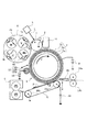
図1は、本実施の形態に係る画像形成装置(本実施の形態では、カラー画像形成可能なレーザービームプリンター)を示す概略構成図である。
【0019】
この画像形成装置は、像担持体としての感光体1、帯電ローラ2、露光装置3、現像装置4、転写装置5、定着装置6などを備えている。
【0020】
感光体1は、本実施の形態では負帯電の有機感光体でアルミニウム製のドラム基体上に光導電層を有しており、所定のプロセススピードで矢印a方向に回転駆動される。
【0021】
帯電ローラ2は、感光体1表面に対して所定の押圧力で圧接され、感光体1の回転駆動に伴い従動回転し、電源(不図示)から帯電ローラ2に対して所定のバイアス電圧(本実施例では、負極性の直流電圧に交流電圧を重畳した電圧)を印加して、感光体1を所定の極性(本実施例では負極性)の電位に帯電処理する。
【0022】
現像装置4は、正規のトナーの極性が負極性のイエロー、マゼンタ、シアン、ブラックトナーをそれぞれ収納する、Y(イエロー)現像器4a,M(マゼンタ)現像器4b,C(シアン)現像器4c,BK(ブラック)現像器4dを備えており、回転駆動装置(不図示)によって矢印b方向に回転し、各Y現像器4a,M現像器4b,C現像器4c,BK現像器4dが現像過程で感光体1と対向するように配設されている。
【0023】
転写装置5は感光体1上のトナー像が1次転写されるローラ状の多層構成の中間転写体7と、中間転写体7上のトナー像を転写材に2次転写する転写ベルト8とを有しており、中間転写体7は、1次転写位置で感光体1表面に当接し、さらに2次転写位置で転写ベルト8表面に当接しており、矢印c方向に感光体1とほぼ同じ周速度で回転駆動される。中間転写体7には1次転写手段としての電源9が接続されており、中間転写体7に所定の1次転写バイアス(直流電圧)を印加する。中間転写体7は、パイプ状の導電性支持体(芯金)7aと、その外周面に形成された弾性層7bと、さらにその上に形成された被覆層7cからなる。
【0024】
転写ベルト8は、2次転写手段としての転写ローラ10aと駆動ローラ10bによって伸張懸架されており、駆動ローラ10bの回転駆動によってベルト上面が矢印d方向に移動する。転写ベルト8は駆動手段(不図示)により、中間転写体7に対して当接離間自在に設置されている。また、転写ローラ10aには電源11が接続されており、転写ローラ10aに所定の2次転写バイアス(直流電圧)を印加する。
【0025】
また、中間転写体7の外周面には、2次転写後、中間転写体7上に残留する転写残トナーに電荷を付与する帯電部材としての、多層構成のローラ12(以下、ICLローラと略す)が当接離間自在に設置されており、中間転写体7には、電源15から所定のバイアス電圧(本実施例では、現像装置4内の正規のトナーの極性とは逆極性(正極性)の直流電圧に交流電圧を重畳した電圧)が印加される。ICLローラ12は、導電性支持体(芯金)12aと、その外周面に形成された弾性層12bと、さらにその上に形成された被覆層12cからなる。
【0026】
次に、上記した画像形成装置の動作について説明する。
【0027】
画像形成時には、感光体1は駆動手段(不図示)により所定のプロセススピードで回転駆動され、所定の帯電バイアス(本実施例では、負極性の直流電圧に交流電圧を重畳した電圧)が印加された帯電ローラ2により所定の極性(負極性)、電位に帯電処理される。
【0028】
そして、帯電された感光体1上に露光装置3によりレーザービームによる画像露光Lが与えられて、目的のカラー画像の第1の色成分像(例えば、イエロー成分像)に対応した静電潜像が形成される。次いで、その静電潜像がY(イエロー)現像器4aにより第1色であるイエロートナーにより現像される。
【0029】
感光体1上に形成担時された前記第1色のイエロートナー画像は、感光体1と中間転写体7との間のニップ部を通過する過程で、このニップ部での圧力と電源9より中間転写体7に印加される1次転写バイアスにより形成される電界とによって、中間転写体7の外周面に1次転写されていく。以下、同様にしてM(マゼンタ)現像器4b,C(シアン)現像器4c,BK(ブラック)現像器4dにより感光体1上にそれぞれ形成担時された第2色のマゼンタトナー画像、第3色のシアンナー画像、第4色のブラックトナー画像が順次中間転写体7上に重畳転写され、目的のカラー画像に対応した合成カラートナー画像が形成される。この工程を1次転写という。
【0030】
この際、感光体1から中間転写体7への第1〜第4色のトナー画像の順次重畳転写のための電源9から印加される1次転写バイアスは、トナーと逆極性(正)である。なお、感光体1から中間転写体7への第1〜第4色のトナー画像の順次重畳転写工程において、転写ベルト8及びICLローラ12は中間転写体7から離間している。
【0031】
そして、給紙カセット(不図示)から紙などの転写材Pがレジストローラ14a,14b、転写前ガイド15を通して中間転写体7と転写ベルト8との間の転写ニップ部(転写ローラ10a近傍)に給送される。この際、電源11より転写ローラ10aへ2次転写バイアス(直流電圧)が印加され、中間転写体7から転写材P上に合成カラートナー画像が転写される。この工程を2次転写という。
【0032】
そして、合成カラートナー画像が転写された転写材Pは、転写ベルト8によっって定着装置6に搬送され、加熱溶着された後に排出される。
【0033】
また、中間転写体7上に2次転写されずに残った2次転写残トナーは、電源13から所定のバイアス(本実施例では、現像装置4内の正規のトナーの極性とは逆極性(正極性)の直流電圧に交流電圧を重畳した電圧)が印加されたICLローラ12によって正極性に転換されて、1次転写位置で中間転写体7に電源9より所定の電圧(正極性)が印加されることにより感光体1へ静電的に転写され、中間転写体7上は清掃化される。このとき、ICLローラ12は中間転写体7に当接している。感光体1上に吸着した2次転写残トナーはその後、クリーニング装置16によって回収される。このとき、感光体1上のトナー像を中間転写体7へ転写するのと同時に、中間転写体7上の転写残トナーを感光体1へ転写する場合は、中間転写体7に所定の1次転写バイアス(正極性)が印加される。本実施例では、ICLローラ12により転写残トナーを正極性に帯電しているが、負極性に帯電してもよい。その際、電源9から中間転写体7に所定の負極性の電圧が印加されることにより、転写残トナーは感光体1へ転写される。
【0034】
本発明者らの実験により、2次転写後、中間転写体7上に残留する転写残トナーに電荷を付与するために、正極性の直流電圧に交流電圧を重畳させた電圧を印加したICLローラ12を用い、このICLローラ12と中間転写体7との表面粗さRzの和を1μm以上50μm以下に調整することにより、長期に安定した転写性及びクリーニング性が得られることを見出した。
【0035】
一方、ICLローラ12に正極性の直流電圧だけを印加して中間転写体7上の転写残トナーの帯電を行った場合には、帯電を受けるのは転写残トナーの最表層だけになってしまう。つまり、トナー層の表層は高い電荷を持った正のトナーとなり、内層部には帯電を比較的受けていないトナーが残ってしまう。このような状態のトナー層をクリーニングしようとすると、以下に述べるようなクリーニング不良とゴーストの2つの問題が発生する。
【0036】
(クリーニング不良)
ICLローラ12を通過して比較的帯電を受けていない内層部のトナーは、次画像にクリーニング不良を発生させてしまう。即ち、クリーニングは、正に帯電された転写残トナーを感光体1と中間転写体7との間の電界で感光体1へ回収することによって行われるため、弱い正もしくは負の電荷を持ったトナーは回収されず、次画像のベタ白部にクリーニング不良のポジゴーストとして現れ、大きな画像欠陥となる。
【0037】
(ネガゴースト)
ICLローラ12を通過した後のトナーの最表層は強く帯電を受けており、その電荷は+50μc/g以上にも達する。このようなトナーは、感光体1と中間転写体7との間の1次転写ニップ(1次転写位置)でクリーニングと同時に、1次転写が行われる次画像のトナーの電荷は、ブラックトナーとして磁性トナーを用いた場合には−10μc/g程度に過ぎない。
【0038】
従って、このようなトナーは、クリーニングされる強い正の電荷を持ったトナーに静電的に吸着されてしまい、中間転写体7に1次転写されることなく感光体1に戻ってしまう。このため、ベタ黒画像を形成しようとしても、前の画像に対応する部分のトナーが感光体1に戻ってしまうため、濃度差を生じ、ネガゴーストとして観察されることになる。具体的には、+50μc/gのICLローラ12通過後の2次転写残トナー1個が、−10μc/gの感光体1から中間転写体7上に1次転写されるべきトナーを5個引き連れてネガゴーストを引き起こすことになるため、2次転写残トナー量が少なくても画像に及ぼす影響は大きくなる。
【0039】
このような現象を防止するためには、ICLローラ12に流す電流を少なくして、2次転写残トナーの最表層に与える電荷を小さくすることが有効であるが、このような対処をすると、2次転写残トナーの内層部のトナーは帯電されないため、クリーニング不良が悪化してしまう。
【0040】
このように、クリーニング不良とネガゴーストとは背反するものであり、ICLローラ12に流す電流を大きくすると、ネガゴーストが激しくなり、小さくすると逆にクリーニング不良が激しくなるため、両者を満足する領域が見出せない。このような現象は、現像されるトナーの電荷が低くなる高湿環境や、もともとの電荷が低い磁性トナー、本実施例ではブラックトナーで顕著になる。高湿環境下では、中抵抗である中間転写体7やICLローラ12が吸湿することで抵抗が低下し、同じ電流を流してもそのほとんどが直接注入電流となってしまうため、放電が発生しにくくなり、トナーを正極性に帯電できないことからクリーニング不良が発生しやすくなる。
【0041】
また、同時に高湿環境下では、現像装置内において、トナーが吸湿し抵抗値が低下することから、特に磁性トナーは、帯電電荷が低下し、ICLローラ12により正極性に帯電された中間転写体7上の2次転写残トナーと1次転写位置で吸着して感光体1に戻ってしまうトナーの数が増えることからネガゴーストも悪化する。
【0042】
この2つの問題を解決するためには、ICLローラ12通過後の2次転写残トナーの電荷を均一化することが必要である。ICLローラ12通過後の2次転写残トナーの最表層の強い正の電荷を持ったトナーがネガゴーストを引き起こし、内層部の弱い電荷のトナーがクリーニング不良を引き起こしているため、2次転写残トナー全体を均一に正に帯電すればこのような問題点を解決することができる。これを実現するために、本実施例では、ICLローラ12に印加する帯電バイアスとして正極性の直流電圧に交流電圧を重畳し、ICLローラ12と中間転写体7との表面粗さRzの和が1μm以上50μm以下となるようにした。
【0043】
つまり、交流電圧を印加することによりICLローラ12からの放電だけでなく、中間転写体7からの逆放電も励起することができ、2次転写残トナーの内層部まで電界を及ぼすことが可能となる。また、さらに高い交流電圧を印加した場合には、ICLローラ12と中間転写体7との間でトナーが飛翔し始めるため、2次転写残トナーの中でトナーの入れ替わりが発生し、さらに均一に帯電することが可能になると同時に、飛翔による2次転写残トナーの散らし効果もあり、さらなるネガゴーストの防止になる。ここで、交流電圧の波形としては、サイン波とは異なり、ピークの時間を長く維持することができることにより、低いピーク間電圧で効率的な2次転写残トナーの帯電や飛翔を起こすことができる矩形波が好ましい。本実施例では、ICLローラ12は中間転写体7に当接して転写残トナーを帯電しているが、上述したような、トナーの飛翔が起こる程度に、離間していても良い。しかし、離間している場合、ICLローラ12に印加する電圧を、当接する場合と比べて大きくする必要があるという欠点がある。
【0044】
しかしながら、ICLローラ12と中間転写体7の表面が粗れていると局所的な放電が発生し、2次転写残トナーの均一な帯電ができなくなってしまい、安定したクリーニングが不可能であった。即ち、ICLローラ12、中間転写体7の表面の凹凸部分のうち、主に、ICLローラ12の凸部と中間転写体7の凸部との間で放電が行われてしまい、中間転写体7の凹部に存在する転写残トナーは帯電不良となってしまった。具体的には、モノカラー画像のクリーニングのように、比較的2次転写残トナー量が少ない場合はクリーニングを良好に行うことが可能であるが、フルカラーモード等での比較的2次転写残トナー量が多い場合には、クリーニングが良好にできない場合があった。
【0045】
このようなことを防止するためには、ICLローラ12と中間転写体7との表面粗さRzの和が50μm以下である必要があった。特に、中間転写体7表面の粗れは、2次転写効率の低下や得られる画像にがさつき等の欠陥を招く恐れがあると同時に、2次転写効率の低下による2次転写残トナー量の増加により、完全にクリーニングできなかった転写残トナーが中間転写体7上に蓄積してしまい、大量に連続してプリントしたとき等にクリーニング不良として画像に現れたり、中間転写体7表面でトナーのフィルミングが発生する等の不具合が生じやすい。
【0046】
このようなことを防止するためには、中間転写体7の表面粗さRzが30μm以下である必要があった。また、ICLローラ12と中間転写体7の表面粗さRzの和が1μm以下の場合、中間転写体7に対するトナーの離型性が悪くなり、2次転写効率が低下するという問題が生じた。さらに、ICLローラ12が中間転写体7の回転と共に回転する従動ローラである場合、上記Rzの和が1μm以下では、ICLローラ12と中間転写体7がスリップしてしまい、均一な2次転写残トナーの帯電ができず、安定したクリーニングが不可能であった。ここで、表面粗さRzは十点平均粗さRzのことであり、ICLローラ12及び中間転写体7の表面粗さRzの測定は、JISのB0601に準拠して測定した値である。
【0047】
次に、上記した中間転写体7及びICLローラ12の構成について詳細に説明する。
【0048】
中間転写体7は、円筒状のステンレス等からなる導電性支持体7a上に弾性層7bを有し、さらにその上に被覆層7cを有している。弾性層7bの厚みは、転写ニップの形成、回転による色ズレ、材料コスト等を考慮して0.5mm以上、好ましくは1〜5mm程度が望ましく、また、被覆層7cの膜厚は、下層の弾性層7bの柔軟性を感光体1表面に伝えるために、500μm以下、好ましくは5〜100μm程度が望ましい。
【0049】
ICLローラ12も同様に、円筒状のステンレス等からなる導電性支持体12a上に弾性層12bを有し、さらにその上に被覆層12cを有している。弾性層12bの厚みは、0.5mm以上、好ましくは1〜5mm程度が望ましく、また、被覆層12cの膜厚は、下層の弾性層12bの柔軟性を損なわないために、500μm以下、好ましくは5〜100μm程度が望ましい。
【0050】
また、上述したように、本発明では中間転写体7の表面粗さRzが30μm以下に形成され、また、中間転写体7とICLローラ12との表面粗さRzの和が1μm以上50μm以下に形成されている(これらの作製については後述する)。
【0051】
中間転写体7及びICLローラ12の各弾性層7b、12b及び被覆層7b、12cにはゴム、エラストマー、樹脂を用いることができる。
【0052】
具体的には、ゴム、エラストマーとしては、天然ゴム、イソプレンゴム、スチレン−ブタジエンゴム、ブタジエンゴム、ブチルゴム、ブタジエンゴム、エチレン−プロピレンゴム、クロロプレンゴム、クロロスルホン化ポリエチレン、塩素化ポリエチレン、アクリロニトリルブタジエンゴム、ウレタンゴム、シンジオタクチック1,2−ポリブタジエン、エピクロルヒドリンゴム、アクリルゴム、シリコーンゴム、フッ素ゴム、多硫化ゴム、ポリノルボルネンゴム、水素化ニトリルゴム、熱可塑性エラストマー(例えば、ポリスチレン系、ポリオレフィン系、ポリ塩化ビニル系、ポリウレタン系、ポリアミド系、ポリエステル系、フッ素樹脂系)を用いることができる。
【0053】
また、樹脂としては、ポリスチレン、クロロポリスチレン、ポリ−α−メチルスチレン、スチレン−ブタジエン共重合体、スチレン−塩化ビニル共重合体、スチレン−酢酸ビニル共重合体、スチレン−マレイン酸共重合体、スチレン−アクリル酸エステル共重合体(スチレン−アクリル酸メチル共重合体、スチレン−アクリル酸エチル共重合体、スチレン−アクリル酸ブチル共重合体、スチレン−アクリル酸オクチル共重合体、及びスチレン−アクリル酸フェニル共重合体等)、スチレン−メタクリル酸エステル共重合体(スチレン−メタクリル酸メチル共重合体、スチレン−メタクリル酸エチル共重合体、スチレン−メタクリル酸フェニル共重合体等)、スチレン−α−クロルアクリル酸メチル共重合体、スチレン−アクリロニトリル−アクリル酸エステル共重合体等のスチレン樹脂(スチレンまたはスチレン置換体を含む単重合体または共重合体)、メタクリル酸メチル樹脂、メタクリル酸ブチル樹脂、アクリル酸エチル樹脂、アクリル酸ブチル樹脂、変形アクリル樹脂(シリコーン変形アクリル樹脂、塩化ビニル変性アクリル樹脂、フッ素変性アクリル樹脂、アクリル・ウレタン樹脂等)、塩化ビニル樹脂、スチレン−酢酸ビニル共重合体、塩化ビニル−酢酸ビニル共重合体、ロジン変性マレイン酸樹脂、フェノール樹脂、エポキシ樹脂、ポリエステル樹脂、ポリウレタン樹脂、ポリエチレン、ポリプロピレン、ポリブタジエン、ポリ塩化ビニリデン、アイオノマー樹脂、シリコーン樹脂、フッ素樹脂、ケトン樹脂、エチレン−エチルアクリレート共重合体、キシレン樹脂及びポリビニルブチラール樹脂、ポリアミド樹脂、変性ポリフェニレンオキサイド樹脂等が挙げられるが、これらに限定されるものではない。また、これらは単独又は共重合ポリマーとして1種又は2種以上混合してもよい。
【0054】
また、中間転写体7及びICLローラ12の各弾性層7b、12b及び被覆層7b、12cには、電気抵抗を調整するために、カーボンブラック、グラファイト、カーボン繊維、金属粉、導電性金属酸化物、有機金属酸化物、有機金属塩、導電性高分子等の導電材を混合分散してもよい。また、トナーの付着防止のために、樹脂粉体や無機粉体を混合分散してもよい。
【0055】
また、中間転写体7及びICLローラ12の導電性支持体7a、12aには、アルミニウム、鉄、ステンレス等の金属、カーボンや金属粉等を分散することにより、導電性を持たせた樹脂等を用いることができる。
【0056】
また、中間転写体7の電気抵抗は103 〜1010Ω(実抵抗)であることが好ましく、好適には104 〜109 Ω(実抵抗)が好ましい。さらに、中間転写体7の表面抵抗は、ICLローラ12と接して放電するために十分な表面抵抗を有している必要があり、その値としては、106 〜1015Ω/□(測定条件:常温・常湿、250V印加時)が有効である。中間転写体7の実抵抗及び表面抵抗の測定法は後述する。
【0057】
また、ICLローラ12の電気抵抗は103 〜1012Ω(実抵抗)であることが好ましく、好適には105 〜1010Ω(実抵抗)が好ましい。さらに、ICLローラ12の表面抵抗は、中間転写体7と接して放電するために十分な表面抵抗を有している必要があり、その値としては、106 〜1015Ω/□(測定条件:常温・常湿、250V印加時)が有効である。また、中間転写体7及びICLローラ12の表面粗さRzを小さくする方法としては、中間転写体7及びICLローラ12の表面部分を研磨するか、中間転写体7及びICLローラ12の被覆層7b、12cを塗装するときに使用する溶剤の組成を工夫する、被覆層7b、12cの乾燥条件を工夫する、塗装方法を工夫する等の方法がある。ICLローラ12の実抵抗及び表面抵抗の測定法は後述する。
【0058】
中間転写体7及びICLローラ12の表面を研磨する方法としては、研削盤を用いる方法、ベルト研剤加工方法、バレル加工法等がある。また、中間転写体7及びICLローラ12の被覆層7b、12cを塗装するときの溶剤の工夫としては、中間転写体7及びICLローラ12の表面が比較的小さなピッチで粗れている場合は、揮発性の低い溶剤を使用すると粗れは改善される傾向にある。
【0059】
また、中間転写体7及びICLローラ12の被覆層7b、12cを塗装する方法としては、ディッピング法、スプレーコーティング法、スピンナーコーティング法、ビードコーティング法、ブレードコーティング法、ビームコーティング法、ロールコーティング法等がある。
【0060】
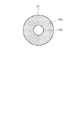
また、上記したICLローラ12は、導電性支持体(芯金)12a上に弾性層12b、被覆層12cを有していたが、これ以外にも、例えば図2に示すように、導電性支持体(芯金)12a上に弾性層12bだけを有する単層構成のICLローラ12や、図3に示すように、導電性支持体(芯金)12a上の弾性層12b上に、2層(あるいは2層以上)の被覆層12c,12dを有する多層構成のICLローラ12でもよい。
【0061】
また、上記した中間転写体7は、導電性支持体(芯金)7a上に弾性層7b、被覆層7cを有していたが、これ以外にも、例えば図4に示すように、導電性支持体(芯金)7a上に弾性層7bだけを有する単層構成の中間転写体7や、図5に示すように、導電性支持体(芯金)7a上の弾性層7b上に、2層(あるいは2層以上)の被覆層7c,7dを有する多層構成の中間転写体7でもよい。
【0062】
更には、図6に示す画像形成装置(カラー画像形成可能なレーザービームプリンター)のように、上記した弾性層上に被覆層を有するベルト状に形成された中間転写体17でもよい。なお、ベルト状の中間転写体17は4個のローラ18a,18b,18c,18dによって伸張懸架されており、電源9が接続されているローラ18aには所定の1次転写バイアス(直流電圧)が印加される。19は転写ローラであり、他の構成は図1に示した画像形成装置と同様である。
【0063】
また、中間転写体7上のフルカラー画像を転写材に2次転写した後、中間転写体7上の転写残トナーをICLローラ12により負極性に帯電し、電源9から中間転写体7に所定の1次転写バイアス(正極性)を印加することで、中間転写体7上の転写残トナーを感光体1へ転写するのと同時に、感光体1上の次画像の1色目のトナー像を中間転写体7へ1次転写することにより(1次転写同時クリーニング)、連続的に画像を形成する際の画像形成のスループットを向上することも可能である。その際、感光体1上へ転写された前記転写残トナーはクリーニング装置16にて回収される。この1次転写同時クリーニングを行うには、転写残トナーを負極性、即ち、感光体1上(現像装置4内)の正規のトナーの極性とは逆極性にICLローラ12により帯電する必要がある。
【0064】
このような構成にすれば、クリーニング不良、ネガゴーストの発生を防止すると共に、画像形成のスループットの向上も図ることができる。更には、中間転写体用の廃トナー容器も不要になるので、装置を小型化することもできる。
【0065】
次に、上記したICLローラ12と中間転写体7、17の作製について詳細に説明する。
【0066】
(実施例1)
ICLローラの作製
直径14mm、長さ340mmのステンレス製芯金上に、下記配合のコンパウンドを金型を用いてトランスファー成形することにより、厚さ3mmの弾性層を有するローラを得た。
【0067】

次に、このローラ上に被覆層を得るための被覆層用塗料を下記処方により作製した。
【0069】
上記塗料を前記ローラにディッピングによりコーティングし、60℃で30分乾燥後、130℃で2時間乾燥することにより残存溶剤を除去し、厚み50μmの被覆層を有するICLローラを得た。得られたICLローラの表面粗さRzは10μmであった。また、実抵抗値は2×10⁸ Ω、表面抵抗は3×10¹²Ω/□であった。ここで、ICLローラの表面粗さRzの測定は、JISのB0601に準拠して測定した値である。
【0071】
ICLローラの実抵抗値は、図7に示す測定装置で測定した。この測定装置は、ICLローラ12に当接する金属ロール(外径50mm)21、直流電源22、抵抗器23、電位差計24を備えている。測定は常温常湿時に行った。
【0072】
ICLローラの実抵抗値測定時には、駆動手段(不図示)によって金属ロール21を回転させ、当接するICLローラ12を従動させる。このときの当接圧は、実際の画像形成時の使用状態と同様に1kgf程度とする。そして、直流電源22から100Vの直流定電圧を金属ロール21に印加し、ICLローラ12の下流側に挿入した、抵抗測定すべきICLローラ12よりも十分に低い既知の抵抗値を有する抵抗器23の両端における電位差を電位差計24にて読む。抵抗器23の両端に得られた電位差から流れる電流Iを求め、この電流値Iを印加電圧100Vで除した値をICLローラ12の実抵抗値とする。
【0073】
なお、ICLローラ12の表面抵抗の測定は、三菱油化製ハイレスタ及びHAプローブを用い、印加電圧250Vで測定した値である。測定は常温常湿時に行った。
【0074】
中間転写体の作製
直径182mm、長さ320mm、厚み5mmのアルミニウム製円筒状ローラ表面に、下記配合のコンパウンドを金型を用いてトランスファー成形することにより、厚さ5mmの弾性層を有するローラを得た。
【0075】
次に、このローラ上に被覆層を得るための被覆層用塗料を下記処方により作製した。
【0077】
上記塗料を前記ローラにディッピングによりコーティングし、60℃で30分乾燥後、130℃で2時間加熱乾燥、硬化することにより、厚み50μmの被覆層を有する中間転写体を得た。得られた中間転写体の表面粗さRzは13μmであった。また、実抵抗値は1×10⁷ Ω、表面抵抗は5×10¹²Ω/□であった。ここで、中間転写体の表面粗さRzの測定は、JISのB0601に準拠して測定した値である。
【0079】
中間転写体の実抵抗値は、図8に示す測定装置で測定した。この測定装置は、中間転写体7に当接する金属ロール(外径40mm)21a、直流電源22a、抵抗器23a、電位差計24aを備えている。測定は常温常湿時に行った。
【0080】
中間転写体7の実抵抗値測定時には、駆動手段(不図示)によって金属ロール21aを回転させ、当接する中間転写体7を周速が100mm/secになるように従動させる。このときの当接圧は、実際の画像形成時の使用状態と同様に2kgf程度とする。そして、直流電源22から1KVの直流定電圧を金属ロール21aに印加し、中間転写体7の下流側に挿入した、測定すべき中間転写体7よりも十分に低い既知の抵抗値を有する抵抗器23aの両端における電位差を電位差計24aにて読む。抵抗器23aの両端に得られた電位差から流れる電流Iを求め、この電流値Iを印加電圧1KVで除した値を中間転写体7の実抵抗値とする。
【0081】
なお、中間転写体7の表面抵抗の測定は、三菱油化製ハイレスタ及びHAプローブを用い、印加電圧250Vで測定した値である。測定は常温常湿時に行った。
【0082】
そして、作製されたICLローラ12と中間転写体7を図1に示す画像形成装置に用い、80g/m2 紙に2次色(ブルー)の文字画像→ベタ黒→2次色(ブルー)の文字画像→ベタ白の4枚連続プリントを行い、2枚目のベタ黒でネガゴーストを、4枚目のベタ白でクリーニング不良を評価した。クリーニング性の評価方法は以下のようにして行った。
【0083】
(クリーニング性評価方法)
ICLローラ12に印加する交流電圧は、中間転写体7からICLローラ12に逆放電が発生し始めるようなピーク間電圧が必要であり、中間転写体7とICLローラ12の放電開始電圧(パッシェンの法則にほぼ従う電圧)の2倍以上のピーク間電圧を有することが望ましく、さらにトナーの飛翔を起こさせる場合にはさらに高い電圧を印加する必要がある。
【0084】
しかしながら、中間転写体7とICLローラ12との間の放電開始電圧を定義することは難しいが、両者の間に直流電圧を印加し、両者の間を流れる電流を測定することで電流電圧特性を表す図9に示すグラフを得た。電流電圧特性の傾きが急に変化し始める電圧を放電開始電圧(パッシェンの法則にほぼ従う)とし、その放電開始電圧の3倍のピーク間電圧を印加した。また、交流電圧の周波数は画像形成装置のプロセススピードから決定され、ピッチ(プロセススピード/周波数)が1mm以下であることが好ましく、今回はピッチが100μmとなるような周波数とした。また、交流電圧の波形としては、サイン波とは異なり、ピークの時間を長く維持することができることにより、低いピーク間電圧で効率的な2次転写残トナーの帯電や飛翔を起こすことのできる矩形波とした。
【0085】
そして、本実施例では、中間転写体7とICLローラ12との間での放電開始電圧が約600Vであったので、ICLローラ12に印加するピーク間電圧を約1800Vとし、プロセススピードが100mm/secであるため、周波数1000Hzとしてクリーニング性の評価、及びフルカラー画像にて5000枚の連続プリント試験を行って連続プリントのクリーニング性の評価を行った。下記に示す表1は、この評価結果を示したものである。
【0086】
【表1】
この評価結果から明らかなように、クリーニング性、及び連続プリントのクリーニング性とも問題なく良好であった。なお、この表において、上記した条件の交流電圧に、ICLローラ12に印加する直流電圧を0〜3000Vの範囲で200V刻みで変化させた電圧を重畳させ、ネガゴーストとクリーニングが両立する組み合わせが存在する場合を○、組み合わせが存在しない場合を×とした。
【0088】
このときの図1に示した画像形成装置における画像形成条件は、以下の通りである。
【0089】
(実施例2)
ICLローラの作製は実施例1と同様である。
【0091】
中間転写体の作製
実施例1に示したゴム配合で得られた弾性層を有するローラ上に、被覆層を得るための被覆層用塗料を実施例1と同様に配合して、この被覆層用塗料をスプレーコーティングし、60℃で30分、120℃で2時間加熱乾燥、硬化させることにより、約30μmの被覆層を有する中間転写体を得た。
【0092】
得られた中間転写体の実抵抗値、表面抵抗、表面粗さRzは、上記した表1に示すように、それぞれ3×10⁷ Ω、1×10¹³Ω/□、33μmであった。これらの測定は実施例1と同様にして行った。
【0093】
次に、実施例1と同様のICLローラと、得られた中間転写体を図1に示した画像形成装置に用い、実施例1と同様のクリーニング性の評価を行った。なお、本実施例では、中間転写体とICLローラとの間での放電開始電圧が約600Vであったので、ICLローラに印加するピーク間電圧を約1800Vとし、プロセススピードが100mm/secであるため、周波数1000Hzとしてクリーニング性の評価、及びフルカラー画像にて5000枚の連続プリント試験を行って連続プリントのクリーニング性の評価を行った。このときの評価結果は、上記した表1の通りである。
【0094】
この評価結果から明らかなように、クリーニング性、及び連続プリントのクリーニング性とも問題なく良好であった。なお、本実施例では、連続プリント後に中間転写体表面に若干のフィルミングが確認されたが、実用上全く問題のないレベルであった。
【0095】
(実施例3)
中間転写体の作製は実施例1と同様である。
【0096】
ICLローラの作製
実施例1に示したゴム配合で得られた弾性層を有するローラ上に、被覆層を得るための被覆層用塗料を実施例1と同様に配合して、この被覆層用塗料をスプレーコーティングし、50℃で30分、100℃で1時間加熱乾燥、硬化させることにより、約50μmの被覆層を有するICLローラを得た。
【0097】
得られた中間転写体の実抵抗値、表面抵抗、表面粗さRzは、上記した表1に示すように、それぞれ4×10⁸ Ω、7×10¹²Ω/□、24μmであった。これらの測定は実施例1と同様にして行った。
【0098】
次に、実施例1と同様の中間転写体と、得られたICLローラを図1に示した画像形成装置に用い、実施例1と同様のクリーニング性の評価を行った。なお、本実施例では、中間転写体とICLローラとの間での放電開始電圧が約600Vであったので、ICLローラに印加するピーク間電圧を約1800Vとし、プロセススピードが100mm/secであるため、周波数1000Hzとしてクリーニング性の評価、及びフルカラー画像にて5000枚の連続プリント試験を行って連続プリントのクリーニング性の評価を行った。このときの評価結果は、上記した表1の通りである。
【0099】
この評価結果から明らかなように、クリーニング性、及び連続プリントのクリーニング性とも問題なく良好であった。
【0100】
(実施例4)
ICLローラの作製は実施例1と同様である。
【0101】
中間転写体の作製
実施例1に示したゴム配合にて、押し出し成形、蒸気加流及び研磨を行い、外径150mm、幅320mm、厚み1mmのゴムベルトを得た。そして、このゴムベルトを外径148mmのアルミシリンダーにはめ込み、実施例1の被覆層用塗料を実施例1と同様の方法にて約50μmの被覆層を形成した後、アルミシリンダーから抜き取って図6に示したようなベルト状の中間転写体17を得た。
【0102】
得られたベルト状の中間転写体の実抵抗値、表面抵抗、表面粗さRzは、上記した表1に示すように、それぞれ4×10⁶ Ω、2×10¹²Ω/□、17μmであった。これらの測定は実施例1と同様にして行った。
【0103】
次に、実施例1と同様のICLローラと得られた中間転写体を図1に示した画像形成装置に用い、実施例1と同様のクリーニング性の評価を行った。なお、本実施例では、中間転写体とICLローラとの間での放電開始電圧が約600Vであったので、ICLローラに印加するピーク間電圧を約1800Vとし、プロセススピードが100mm/secであるため、周波数1000Hzとしてクリーニング性の評価、及びフルカラー画像にて5000枚の連続プリント試験を行って連続プリントのクリーニング性の評価を行った。このときの評価結果は、上記した表1の通りである。
【0104】
この評価結果から明らかなように、クリーニング性、及び連続プリントのクリーニング性とも問題なく良好であった。なお、本実施例では、連続プリント後の画像に若干の色ズレが確認されたが、実用上全く問題のないレベルであった。
【0105】
(比較例1)
実施例1と同様のICLローラと中間転写体を図1に示した画像形成装置に用いた。この比較例では、ICLローラには正極性の直流電圧のみを印加して実施例1と同様の条件でクリーニング性の評価を行った。このときの評価結果は、上記した表1の通りである。
【0106】
この評価結果から明らかなように、ICLローラに直流電圧のみを印加した場合では、クリーニングとネガゴーストを両立する条件は見出せず、また、初期からクリーニング性が悪く、連続プリントのクリーニング性試験は行わなかった。
【0107】
(比較例2)
ICLローラは実施例1と同様であり、中間転写体は、実施例2で中間転写体被覆層用の塗料配合中のキシレンをトルエンに、エタノールをメタノールに変更した以外は実施例2と同様の条件にして作製した。
【0108】
得られた中間転写体の実抵抗値、表面抵抗、表面粗さRzは上記した表1に示すように、それぞれ4×10⁷ Ω、2×10¹³Ω/□、44μmであった。これらの測定は実施例1と同様にして行った。
【0109】
次に、実施例1と同様のICLローラと得られた中間転写体を図1に示した画像形成装置に用い、実施例1と同様にクリーニング性の評価を行った。なお、この比較例では、中間転写体とICLローラ間での放電開始電圧は約600Vであったので、ICLローラに印加するピーク間電圧を約1800Vとし、プロセススピードが100mm/secであるため、周波数は1000Hzとしてクリーニング性の評価を行った。このときの評価結果は、上記した表1の通りである。
【0110】
この評価結果から明らかなように、中間転写体の被覆層用の塗料配合を変えた場合では、クリーニングとネガゴーストを両立する条件は見出せず、また、初期からクリーニング性が悪く、連続プリントのクリーニング性試験は行わなかった。
【0111】
(比較例3)
ICLローラは、実施例1で得られたICLローラの表面を研磨したものを用いた。得られたICLローラの実抵抗値、表面抵抗、表面粗さRzは上記した表1に示すように、それぞれ5×10⁷ Ω、6×10¹¹Ω/□、0.4μmであった。これらの測定は実施例1と同様にして行った。
【0112】
中間転写体は、実施例1で得られた中間転写体の表面を研磨したものを用いた。得られた中間転写体の実抵抗値、表面抵抗、表面粗さRzは上記した表1に示すように、それぞれ6×10⁶ Ω、8×10¹¹Ω/□、0.4μmであった。これらの測定は実施例1と同様にして行った。
【0113】
次に、これらのICLローラと中間転写体を図1に示した画像形成装置に用い、実施例1と同様にクリーニング性の評価を行った。なお、この比較例では、中間転写体とICLローラ間での放電開始電圧は約600Vであったので、ICLローラに印加するピーク間電圧を約1800Vとし、プロセススピードが100mm/secであるため、周波数は1000Hzとしてクリーニング性の評価を行った。このときの評価結果は、上記した表1の通りである。
【0114】
この評価結果から明らかなように、ICLローラと中間転写体の表面を十分に研磨した場合では、クリーニングとネガゴーストを両立する条件は見出せず、また、初期からクリーニング性が悪く、連続プリントのクリーニング性試験は行わなかった。
【0115】
【発明の効果】
以上説明したように、本発明によれば、中間転写体と帯電部材の表面粗さRzの和を1μm以上50μm以下としたことにより、繰り返し良好な中間転写体のクリーニングが可能となり、長期にわたって良好な画像形成を行うことができる。
【0116】
更に、像担持体から中間転写体へトナー像を1次転写するのと同時に、中間転写体から像担持体へ転写残トナーを転写することで、画像形成のスループットの向上も図ることができる。
【図面の簡単な説明】
【図1】本発明の実施の形態に係る画像形成装置を示す概略構成図。
【図2】本発明の実施の形態に係る画像形成装置のICLローラの一例を示す断面図。
【図3】本発明の実施の形態に係る画像形成装置のICLローラの一例を示す断面図。
【図4】本発明の実施の形態に係る画像形成装置の中間転写体の一例を示す断面図。
【図5】本発明の実施の形態に係る画像形成装置の中間転写体の一例を示す断面図。
【図6】ベルト状に形成された中間転写体を備えた本発明の実施の形態に係る画像形成装置を示す概略構成図。
【図7】ICLローラの抵抗を測定する測定装置を示す概略図。
【図8】中間転写体の抵抗を測定する測定装置を示す概略図。
【図9】中間転写体とICLローラとの間の電流−電圧特性を示す図。
【符号の説明】
1 感光体
2 帯電ローラ
4 現像装置
5 転写装置
6 定着装置
7 中間転写体
7a 導電性支持体
7b 弾性層
7c 被覆層
8、17 転写ベルト
12 ICLローラ
12a 導電性支持体
12b 弾性層
12c 被覆層
13 クリーニングバイアス電源(電源)[0001]
BACKGROUND OF THE INVENTION
The present invention relates to an image forming apparatus using an electrophotographic process, and in particular, a toner image formed on an image carrier is temporarily transferred onto an intermediate transfer member, and the toner image transferred to the intermediate transfer member is transferred. The present invention relates to an image forming apparatus such as a copying machine, a laser beam printer, and a facsimile machine that forms an image by secondary transfer to a material by a contact transfer member.
[0002]
[Prior art]
A toner image formed on a drum-type electrophotographic photosensitive member (hereinafter referred to as a photosensitive member) as an image carrier is temporarily transferred onto the intermediate transfer member, and the toner image transferred to the intermediate transfer member is transferred. An image forming apparatus that performs image transfer by secondary transfer to a material with a contact transfer member sequentially stacks and transfers a plurality of component color images of color image information and multicolor image information to synthesize and reproduce a color image and a multicolor image. It is effective as a color image forming apparatus or multicolor image forming apparatus for outputting an image formed product, or an image forming apparatus having a color image forming function or a multicolor image forming function. ).
[0003]
By the way, in the image forming apparatus described above, it is possible to remove (clean) the transfer residual toner remaining on the intermediate transfer member after the secondary transfer from the intermediate transfer member to a transfer material such as paper. Is important.
[0004]
For this reason, in this type of conventional image forming apparatus, for example, the following methods (a) to (d) for removing transfer residual toner remaining on the intermediate transfer member have been proposed.
[0005]
(A) An elastic blade is brought into contact with and separated from the intermediate transfer member, and the transfer residual toner on the intermediate transfer member is scraped off (for example, Japanese Patent Laid-Open Nos. 56-153357 and 5-303310).
[0006]
(B) A fur brush that comes in contact with and separates from the intermediate transfer member is applied, and a bias having a polarity opposite to that of the transfer residual toner on the intermediate transfer member is applied to recover the transfer residual toner, which is once adhered to a bias roller such as a metal roller. Then scrape with a blade.
[0007]
(C) In order to reduce the above-mentioned blade cleaning burden, the transfer residual toner on the intermediate transfer member is returned onto the photosensitive member by an electric field (for example, JP-A-4-340564, JP-A-5-277739, etc.) ).
[0008]
(D) In order to eliminate the waste of providing similar cleaning devices for both the intermediate transfer member and the photosensitive member and simplify the cleaning device configuration, the transfer residual toner on the intermediate transfer member is reversed to the charged potential of the photosensitive member. A charging device for charging to polarity is provided, and the transfer residual toner on the intermediate transfer member is returned to the photosensitive member only by the action of the charging device (for example, JP-A-1-105980).
[0009]
[Problems to be solved by the invention]
By the way, in the removal method in which the transfer residual toner is cleaned only by a mechanical force using the elastic blades or brushes of (a) and (b) described above, the transfer residual toner is easy to slip through and easily causes defective cleaning. Furthermore, there is a problem that repeated cleaning causes wear of the cleaning member, and cleaning defects are more likely to occur.
[0010]
The cleaning method (c) using both the mechanical force and the electrostatic force is effective because it differs from the mechanical means as described above. However, the normal printing step for image formation is effective. In addition, there is a need for a cleaning step for cleaning the transfer residual toner on the intermediate transfer member, and it is impossible to continuously print images of different patterns, resulting in a problem that the throughput of image formation is remarkably reduced.
[0011]
In the above (d), a charging device is provided for charging the transfer residual toner on the intermediate transfer member to a polarity opposite to the charging potential of the photosensitive member, and the transfer residual toner on the intermediate transfer member is applied to the photosensitive member only by the charging device. The return configuration is very simple and seems to be an effective means. However, as in (c), a cleaning step for cleaning the transfer residual toner on the intermediate transfer member is provided separately from the normal printing step for forming an image.
[0012]
Accordingly, even in this case, a decrease in throughput of image formation becomes a problem.
[0013]
Further, if the transfer residual toner on the intermediate transfer member cannot be uniformly charged, the transfer residual toner on the intermediate transfer member cannot be electrostatically returned to the photosensitive member and remains on the intermediate transfer member as it is. A cleaning failure occurred.
[0014]
Furthermore, in order to improve the throughput of image formation, the transfer residual toner on the intermediate transfer member is electrostatically returned to the photosensitive member, and at the same time, the next toner image on the photosensitive member is transferred to the intermediate transfer member. In the apparatus, the above-described poor cleaning has a big problem because it affects the next image.
[0015]
SUMMARY An advantage of some aspects of the invention is that it provides an image forming apparatus capable of repeatedly cleaning the transfer residual toner on the intermediate transfer member repeatedly.
[0016]
Furthermore, an object of the present invention is to provide an image forming apparatus capable of improving the throughput of image formation while satisfactorily cleaning the transfer residual toner on the intermediate transfer member.
[0017]
[Means for Solving the Problems]
The above objective is accomplished by the present invention. The present invention includes an image carrier that carries a toner image, an intermediate transfer member on which the toner image on the image carrier is electrostatically primary-transferred at a primary transfer position, A voltage obtained by superimposing an AC voltage on a DC voltage having a polarity opposite to that of normal toner on the image carrier is applied. A charging member; The charging member charges residual toner remaining on the intermediate transfer member after the toner image on the intermediate transfer member is secondarily transferred to a transfer material, In the image forming apparatus in which the residual toner charged by the charging member is transferred to the image carrier at the primary transfer position, the sum of the surface roughness Rz of the intermediate transfer member and the surface roughness Rz of the charging member. Is 1 μm or more and 50 μm or less.
[0018]
DETAILED DESCRIPTION OF THE INVENTION
FIG. 1 is a schematic configuration diagram showing an image forming apparatus according to the present embodiment (in this embodiment, a laser beam printer capable of forming a color image).
[0019]
The image forming apparatus includes a
[0020]
In this embodiment, the
[0021]
The charging roller 2 is pressed against the surface of the
[0022]
The developing device 4 stores yellow, magenta, cyan, and black toners having normal toner polarities of negative polarity, Y (yellow)
[0023]
The
[0024]
The transfer belt 8 is stretched and suspended by a
[0025]
Further, on the outer peripheral surface of the
[0026]
Next, the operation of the above-described image forming apparatus will be described.
[0027]
At the time of image formation, the
[0028]
Then, an electrostatic exposure image corresponding to a first color component image (for example, a yellow component image) of a target color image is provided on the charged
[0029]
The yellow toner image of the first color formed on the
[0030]
At this time, the primary transfer bias applied from the
[0031]
Then, a transfer material P such as paper from a paper feed cassette (not shown) passes through
[0032]
Then, the transfer material P onto which the composite color toner image has been transferred is conveyed to the fixing device 6 by the transfer belt 8 and is discharged after being heated and welded.
[0033]
Further, the secondary transfer residual toner remaining on the
[0034]
According to the experiments of the present inventors, an ICL roller to which a voltage obtained by superimposing an AC voltage on a positive DC voltage is applied in order to charge the residual toner remaining on the
[0035]
On the other hand, when only the positive DC voltage is applied to the
[0036]
(Cleaning failure)
The toner in the inner layer portion that passes through the
[0037]
(Negative ghost)
The outermost layer of the toner after passing through the
[0038]
Therefore, such toner is electrostatically attracted to the toner having a strong positive charge to be cleaned, and returns to the
[0039]
In order to prevent such a phenomenon, it is effective to reduce the electric current applied to the
[0040]
As described above, the poor cleaning and the negative ghost are contrary to each other. When the current flowing through the
[0041]
At the same time, in a high-humidity environment, the toner absorbs moisture and the resistance value decreases in the developing device. In particular, the magnetic toner has a lower charge and is charged positively by the
[0042]
In order to solve these two problems, it is necessary to make the charge of the secondary transfer residual toner after passing through the
[0043]
That is, by applying an AC voltage, not only the discharge from the
[0044]
However, if the surfaces of the
[0045]
In order to prevent this, the sum of the surface roughness Rz of the
[0046]
In order to prevent this, the surface roughness Rz of the
[0047]
Next, the configuration of the
[0048]
The
[0049]
Similarly, the
[0050]
Further, as described above, in the present invention, the surface roughness Rz of the
[0051]
Rubber, elastomer, or resin can be used for the
[0052]
Specifically, as rubber and elastomer, natural rubber, isoprene rubber, styrene-butadiene rubber, butadiene rubber, butyl rubber, butadiene rubber, ethylene-propylene rubber, chloroprene rubber, chlorosulfonated polyethylene, chlorinated polyethylene, acrylonitrile butadiene rubber , Urethane rubber, syndiotactic 1,2-polybutadiene, epichlorohydrin rubber, acrylic rubber, silicone rubber, fluorine rubber, polysulfide rubber, polynorbornene rubber, hydrogenated nitrile rubber, thermoplastic elastomer (for example, polystyrene series, polyolefin series, (Polyvinyl chloride, polyurethane, polyamide, polyester, fluororesin) can be used.
[0053]
Examples of the resin include polystyrene, chloropolystyrene, poly-α-methylstyrene, styrene-butadiene copolymer, styrene-vinyl chloride copolymer, styrene-vinyl acetate copolymer, styrene-maleic acid copolymer, styrene. -Acrylate ester copolymer (styrene-methyl acrylate copolymer, styrene-ethyl acrylate copolymer, styrene-butyl acrylate copolymer, styrene-octyl acrylate copolymer, and styrene-phenyl acrylate copolymer) Copolymer), styrene-methacrylic acid ester copolymer (styrene-methyl methacrylate copolymer, styrene-ethyl methacrylate copolymer, styrene-phenyl methacrylate copolymer, etc.), styrene-α-chloroacryl. Acid methyl copolymer, styrene-acrylonitrile-acrylic acid Styrene resin (monopolymer or copolymer containing styrene or styrene-substituted product), methyl methacrylate resin, butyl methacrylate resin, ethyl acrylate resin, butyl acrylate resin, modified acrylic resin (Silicone modified acrylic resin, vinyl chloride modified acrylic resin, fluorine modified acrylic resin, acrylic / urethane resin, etc.), vinyl chloride resin, styrene-vinyl acetate copolymer, vinyl chloride-vinyl acetate copolymer, rosin modified maleic acid resin Phenol resin, epoxy resin, polyester resin, polyurethane resin, polyethylene, polypropylene, polybutadiene, polyvinylidene chloride, ionomer resin, silicone resin, fluorine resin, ketone resin, ethylene-ethyl acrylate copolymer, xylene resin and Polyvinyl butyral resin, polyamide resin, modified polyphenylene oxide resins, but is not limited thereto. These may be used alone or in combination as a copolymer.
[0054]
In addition, the
[0055]
The
[0056]
Further, the electric resistance of the
[0057]
The electrical resistance of the
[0058]
Examples of methods for polishing the surfaces of the
[0059]
The
[0060]
The
[0061]
The
[0062]
Furthermore, as in the image forming apparatus (laser beam printer capable of forming a color image) shown in FIG. 6, the
[0063]
Further, after the full-color image on the
[0064]
With such a configuration, it is possible to prevent defective cleaning and negative ghosts and improve the throughput of image formation. Further, since the waste toner container for the intermediate transfer member is not required, the apparatus can be reduced in size.
[0065]
Next, the production of the
[0066]
(Example 1)
Production of ICL roller
A roller having an elastic layer having a thickness of 3 mm was obtained by transfer molding a compound having the following composition on a stainless steel core having a diameter of 14 mm and a length of 340 mm using a mold.
[0067]
Next, a coating material for a coating layer for obtaining a coating layer on the roller was prepared according to the following formulation.
[0069]
The paint was coated on the roller by dipping, dried at 60 ° C. for 30 minutes, and then dried at 130 ° C. for 2 hours to remove residual solvent, thereby obtaining an ICL roller having a coating layer having a thickness of 50 μm. The surface roughness Rz of the obtained ICL roller was 10 μm. The actual resistance value is 2 × 10 8 Ω, surface resistance is 3 × 10 12 It was Ω / □. Here, the measurement of the surface roughness Rz of the ICL roller is a value measured according to JIS B0601.
[0071]
The actual resistance value of the ICL roller was measured with a measuring apparatus shown in FIG. This measuring apparatus includes a metal roll (outer diameter 50 mm) 21 that contacts the
[0072]
At the time of measuring the actual resistance value of the ICL roller, the
[0073]
The measurement of the surface resistance of the
[0074]
Preparation of intermediate transfer member
A roller having an elastic layer having a thickness of 5 mm was obtained by transfer molding a compound having the following composition on the surface of an aluminum cylindrical roller having a diameter of 182 mm, a length of 320 mm, and a thickness of 5 mm using a mold.
[0075]
Next, a coating material for a coating layer for obtaining a coating layer on the roller was prepared according to the following formulation.
[0077]
The paint was coated on the roller by dipping, dried at 60 ° C. for 30 minutes, dried by heating at 130 ° C. for 2 hours, and cured to obtain an intermediate transfer member having a coating layer having a thickness of 50 μm. The surface roughness Rz of the obtained intermediate transfer member was 13 μm. The actual resistance value is 1 × 10 7 Ω, surface resistance is 5 × 10 12 It was Ω / □. Here, the measurement of the surface roughness Rz of the intermediate transfer member is a value measured according to JIS B0601.
[0079]
The actual resistance value of the intermediate transfer member was measured with a measuring apparatus shown in FIG. This measuring apparatus includes a metal roll (outer diameter 40 mm) 21 a that contacts the
[0080]
At the time of measuring the actual resistance value of the
[0081]
The measurement of the surface resistance of the
[0082]
The produced
[0083]
(Cleaning evaluation method)
The AC voltage applied to the
[0084]
However, although it is difficult to define the discharge start voltage between the
[0085]
In this embodiment, since the discharge start voltage between the
[0086]
[Table 1]
As is clear from the evaluation results, the cleaning property and the cleaning property of continuous printing were satisfactory without problems. In this table, there is a combination in which the negative ghost and the cleaning are compatible by superimposing the voltage obtained by changing the DC voltage applied to the
[0088]
The image forming conditions in the image forming apparatus shown in FIG. 1 at this time are as follows.
[0089]
(Example 2)
The production of the ICL roller is the same as in Example 1.
[0091]
Preparation of intermediate transfer member
The coating material for coating layer for obtaining the coating layer was compounded in the same manner as in Example 1 on the roller having the elastic layer obtained by the rubber compounding shown in Example 1, and this coating material for coating layer was spray coated. Then, an intermediate transfer member having a coating layer of about 30 μm was obtained by heating, drying and curing at 60 ° C. for 30 minutes and at 120 ° C. for 2 hours.
[0092]
The actual resistance value, surface resistance, and surface roughness Rz of the obtained intermediate transfer member were 3 × 10 3 as shown in Table 1 above. 7 Ω, 1 × 10 13 Ω / □, 33 μm. These measurements were performed in the same manner as in Example 1.
[0093]
Next, the same ICL roller as in Example 1 and the obtained intermediate transfer member were used in the image forming apparatus shown in FIG. In this embodiment, since the discharge start voltage between the intermediate transfer member and the ICL roller is about 600 V, the peak-to-peak voltage applied to the ICL roller is about 1800 V, and the process speed is 100 mm / sec. Therefore, the cleaning performance was evaluated at a frequency of 1000 Hz, and the continuous printing test was performed on 5000 sheets of full-color images to evaluate the cleaning performance of continuous printing. The evaluation results at this time are as shown in Table 1 above.
[0094]
As is clear from the evaluation results, the cleaning property and the cleaning property of continuous printing were satisfactory without problems. In this example, a slight filming was confirmed on the surface of the intermediate transfer member after continuous printing, but it was at a level that causes no problem in practical use.
[0095]
(Example 3)
The production of the intermediate transfer member is the same as in Example 1.
[0096]
Production of ICL roller
The coating material for coating layer for obtaining the coating layer was compounded in the same manner as in Example 1 on the roller having the elastic layer obtained by the rubber compounding shown in Example 1, and this coating material for coating layer was spray coated. The ICL roller having a coating layer of about 50 μm was obtained by heating, drying and curing at 50 ° C. for 30 minutes and at 100 ° C. for 1 hour.
[0097]
The actual resistance value, surface resistance, and surface roughness Rz of the obtained intermediate transfer member were 4 × 10 4 as shown in Table 1 above. 8 Ω, 7 × 10 12 Ω / □, 24 μm. These measurements were performed in the same manner as in Example 1.
[0098]
Next, the same intermediate transfer member as in Example 1 and the obtained ICL roller were used in the image forming apparatus shown in FIG. In this embodiment, since the discharge start voltage between the intermediate transfer member and the ICL roller is about 600 V, the peak-to-peak voltage applied to the ICL roller is about 1800 V, and the process speed is 100 mm / sec. Therefore, the cleaning performance was evaluated at a frequency of 1000 Hz, and the continuous printing test was performed on 5000 sheets of full-color images to evaluate the cleaning performance of continuous printing. The evaluation results at this time are as shown in Table 1 above.
[0099]
As is clear from the evaluation results, the cleaning property and the cleaning property of continuous printing were satisfactory without problems.
[0100]
Example 4
The production of the ICL roller is the same as in Example 1.
[0101]
Preparation of intermediate transfer member
Extrusion molding, steam heating and polishing were carried out with the rubber composition shown in Example 1 to obtain a rubber belt having an outer diameter of 150 mm, a width of 320 mm and a thickness of 1 mm. Then, this rubber belt was fitted into an aluminum cylinder having an outer diameter of 148 mm, and the coating material for the coating layer of Example 1 was formed in the same manner as in Example 1 to form a coating layer of about 50 μm. A belt-like
[0102]
The actual resistance value, surface resistance, and surface roughness Rz of the obtained belt-shaped intermediate transfer member are 4 × 10 4 as shown in Table 1 above. 6 Ω, 2 × 10 12 Ω / □, 17 μm. These measurements were performed in the same manner as in Example 1.
[0103]
Next, the same ICL roller as in Example 1 and the obtained intermediate transfer member were used in the image forming apparatus shown in FIG. In this embodiment, since the discharge start voltage between the intermediate transfer member and the ICL roller is about 600 V, the peak-to-peak voltage applied to the ICL roller is about 1800 V, and the process speed is 100 mm / sec. Therefore, the cleaning performance was evaluated at a frequency of 1000 Hz, and the continuous printing test was performed on 5000 sheets of full-color images to evaluate the cleaning performance of continuous printing. The evaluation results at this time are as shown in Table 1 above.
[0104]
As is clear from the evaluation results, the cleaning property and the cleaning property of continuous printing were satisfactory without problems. In this example, a slight color shift was confirmed in the image after continuous printing, but it was at a level of no problem in practical use.
[0105]
(Comparative Example 1)
The same ICL roller and intermediate transfer member as in Example 1 were used in the image forming apparatus shown in FIG. In this comparative example, only the positive DC voltage was applied to the ICL roller, and the cleaning property was evaluated under the same conditions as in Example 1. The evaluation results at this time are as shown in Table 1 above.
[0106]
As is clear from this evaluation result, when only a DC voltage is applied to the ICL roller, no conditions for achieving both cleaning and negative ghost are found, and the cleaning property is poor from the beginning. There wasn't.
[0107]
(Comparative Example 2)
The ICL roller is the same as in Example 1, and the intermediate transfer member is the same as in Example 2 except that xylene in the coating composition for the intermediate transfer member coating layer in Example 2 is changed to toluene and ethanol is changed to methanol. Produced under conditions.
[0108]
The actual resistance value, surface resistance, and surface roughness Rz of the obtained intermediate transfer member were 4 × 10 4 as shown in Table 1 above. 7 Ω, 2 × 10 13 Ω / □, 44 μm. These measurements were performed in the same manner as in Example 1.
[0109]
Next, the same ICL roller as in Example 1 and the obtained intermediate transfer member were used in the image forming apparatus shown in FIG. In this comparative example, since the discharge start voltage between the intermediate transfer member and the ICL roller was about 600 V, the peak-to-peak voltage applied to the ICL roller was about 1800 V, and the process speed was 100 mm / sec. The cleaning property was evaluated at a frequency of 1000 Hz. The evaluation results at this time are as shown in Table 1 above.
[0110]
As is apparent from this evaluation result, when the coating composition for the coating layer of the intermediate transfer member is changed, conditions for achieving both cleaning and negative ghost cannot be found, and cleaning performance is poor from the beginning, and continuous printing cleaning is not possible. No sex test was performed.
[0111]
(Comparative Example 3)
As the ICL roller, one obtained by polishing the surface of the ICL roller obtained in Example 1 was used. The actual resistance value, surface resistance, and surface roughness Rz of the obtained ICL roller were 5 × 10 5 as shown in Table 1 above. 7 Ω, 6 × 10 11 Ω / □, 0.4 μm. These measurements were performed in the same manner as in Example 1.
[0112]
As the intermediate transfer member, the surface of the intermediate transfer member obtained in Example 1 was polished. The actual resistance value, surface resistance, and surface roughness Rz of the obtained intermediate transfer member were 6 × 10 6 as shown in Table 1 above. 6 Ω, 8 × 10 11 Ω / □, 0.4 μm. These measurements were performed in the same manner as in Example 1.
[0113]
Next, these ICL rollers and the intermediate transfer member were used in the image forming apparatus shown in FIG. In this comparative example, since the discharge start voltage between the intermediate transfer member and the ICL roller was about 600 V, the peak-to-peak voltage applied to the ICL roller was about 1800 V, and the process speed was 100 mm / sec. The cleaning property was evaluated at a frequency of 1000 Hz. The evaluation results at this time are as shown in Table 1 above.
[0114]
As is clear from this evaluation result, when the surfaces of the ICL roller and the intermediate transfer member are sufficiently polished, conditions for achieving both cleaning and negative ghost cannot be found, and cleaning performance is poor from the beginning, and continuous printing cleaning is not possible. No sex test was performed.
[0115]
【The invention's effect】
As described above, according to the present invention, since the sum of the surface roughness Rz of the intermediate transfer member and the charging member is 1 μm or more and 50 μm or less, the intermediate transfer member can be repeatedly and repeatedly cleaned, which is good for a long time. Image formation can be performed.
[0116]
Further, by simultaneously transferring the toner image from the image carrier to the intermediate transfer member, and simultaneously transferring the transfer residual toner from the intermediate transfer member to the image carrier, the throughput of image formation can be improved.
[Brief description of the drawings]
FIG. 1 is a schematic configuration diagram illustrating an image forming apparatus according to an embodiment of the present invention.
FIG. 2 is a cross-sectional view showing an example of an ICL roller of the image forming apparatus according to the embodiment of the present invention.
FIG. 3 is a cross-sectional view showing an example of an ICL roller of the image forming apparatus according to the embodiment of the present invention.
FIG. 4 is a cross-sectional view showing an example of an intermediate transfer member of the image forming apparatus according to the embodiment of the present invention.
FIG. 5 is a cross-sectional view showing an example of an intermediate transfer member of the image forming apparatus according to the embodiment of the present invention.
FIG. 6 is a schematic configuration diagram illustrating an image forming apparatus according to an embodiment of the present invention that includes an intermediate transfer member formed in a belt shape.
FIG. 7 is a schematic view showing a measuring device for measuring the resistance of an ICL roller.
FIG. 8 is a schematic view showing a measuring apparatus for measuring the resistance of an intermediate transfer member.
FIG. 9 is a diagram illustrating current-voltage characteristics between an intermediate transfer member and an ICL roller.
[Explanation of symbols]
1 Photoconductor
2 Charging roller
4 Development device
5 Transfer device
6 Fixing device
7 Intermediate transfer member
7a Conductive support
7b Elastic layer
7c Coating layer
8, 17 Transfer belt
12 ICL Roller
12a Conductive support
12b Elastic layer
12c coating layer
13 Cleaning bias power supply
Claims (5)
前記中間転写体の表面粗さRzと前記帯電部材の表面粗さRzの和は1μm以上50μm以下であることを特徴とする画像形成装置。An image carrier that carries a toner image, an intermediate transfer body on which the toner image on the image carrier is electrostatically primary-transferred at a primary transfer position, and the polarity of regular toner on the image carrier. And a charging member to which a voltage obtained by superimposing an AC voltage on a DC voltage having a reverse polarity is applied. After the toner image on the intermediate transfer member is secondarily transferred to the transfer material, In the image forming apparatus, the residual toner remaining on the intermediate transfer member is charged, and the residual toner charged by the charging member is transferred to the image carrier at the primary transfer position.
The sum of the surface roughness Rz of the intermediate transfer member and the surface roughness Rz of the charging member is 1 μm or more and 50 μm or less.
Priority Applications (4)
| Application Number | Priority Date | Filing Date | Title |
|---|---|---|---|
| JP02974798A JP4114991B2 (en) | 1997-02-21 | 1998-02-12 | Image forming apparatus |
| EP98301278A EP0860751B1 (en) | 1997-02-21 | 1998-02-20 | Image forming apparatus |
| DE1998621148 DE69821148T2 (en) | 1997-02-21 | 1998-02-20 | Image forming apparatus |
| US09/026,947 US5950058A (en) | 1997-02-21 | 1998-02-20 | Image forming apparatus |
Applications Claiming Priority (3)
| Application Number | Priority Date | Filing Date | Title |
|---|---|---|---|
| JP3816297 | 1997-02-21 | ||
| JP9-38162 | 1997-02-21 | ||
| JP02974798A JP4114991B2 (en) | 1997-02-21 | 1998-02-12 | Image forming apparatus |
Publications (2)
| Publication Number | Publication Date |
|---|---|
| JPH10293480A JPH10293480A (en) | 1998-11-04 |
| JP4114991B2 true JP4114991B2 (en) | 2008-07-09 |
Family
ID=26367983
Family Applications (1)
| Application Number | Title | Priority Date | Filing Date |
|---|---|---|---|
| JP02974798A Expired - Fee Related JP4114991B2 (en) | 1997-02-21 | 1998-02-12 | Image forming apparatus |
Country Status (4)
| Country | Link |
|---|---|
| US (1) | US5950058A (en) |
| EP (1) | EP0860751B1 (en) |
| JP (1) | JP4114991B2 (en) |
| DE (1) | DE69821148T2 (en) |
Cited By (1)
| Publication number | Priority date | Publication date | Assignee | Title |
|---|---|---|---|---|
| US8591647B2 (en) | 1999-06-09 | 2013-11-26 | Ricoh Company, Ltd. | Production of a GaN bulk crystal substrate and a semiconductor device formed thereon |
Families Citing this family (7)
| Publication number | Priority date | Publication date | Assignee | Title |
|---|---|---|---|---|
| JP3792902B2 (en) | 1997-08-04 | 2006-07-05 | キヤノン株式会社 | Image forming apparatus |
| US6115576A (en) * | 1998-05-01 | 2000-09-05 | Ricoh Company, Ltd. | Image forming apparatus using a developing liquid and including an intermediate transfer body |
| WO2001022173A1 (en) * | 1999-09-20 | 2001-03-29 | Hitachi, Ltd. | Electrophotographic image forming device, intermediate transfer body and electrophotograpic image forming method |
| US6516176B1 (en) * | 2001-08-13 | 2003-02-04 | Toshiba Tec Kabushiki Kaisha | Transferring body apparatus with elastic member covering surface of base of the transferring body apparatus |
| JP3927781B2 (en) * | 2001-08-31 | 2007-06-13 | キヤノン株式会社 | Process cartridge and intermediate transfer belt |
| US8783137B2 (en) * | 2006-04-14 | 2014-07-22 | Blohm + Voss Oil Tools, Llc | Apparatus for spinning drill pipe |
| US8219011B2 (en) * | 2007-02-26 | 2012-07-10 | Konica Minolta Business Technologies, Inc. | Intermediate transfer member and image formation apparatus |
Family Cites Families (18)
| Publication number | Priority date | Publication date | Assignee | Title |
|---|---|---|---|---|
| JPS56153357A (en) * | 1980-04-29 | 1981-11-27 | Konishiroku Photo Ind Co Ltd | Copying device |
| JPS5950475A (en) * | 1982-09-17 | 1984-03-23 | Konishiroku Photo Ind Co Ltd | Intermediate transfer material |
| JPS63194272A (en) * | 1987-02-09 | 1988-08-11 | Sharp Corp | Image forming device |
| JPH01105980A (en) * | 1987-10-19 | 1989-04-24 | Sharp Corp | Image forming device having residual matter transfer mechanism |
| JPH04303869A (en) * | 1991-03-30 | 1992-10-27 | Tokai Rubber Ind Ltd | Endless belt for intermediate transfer |
| JPH04340564A (en) * | 1991-05-16 | 1992-11-26 | Matsushita Electric Ind Co Ltd | Color image forming device |
| JP3193113B2 (en) * | 1992-04-21 | 2001-07-30 | 株式会社リコー | Image forming method |
| JP3057121B2 (en) * | 1992-04-28 | 2000-06-26 | 株式会社リコー | Image forming device |
| JP3193796B2 (en) * | 1992-12-29 | 2001-07-30 | キヤノン株式会社 | Image forming device |
| JP3119047B2 (en) * | 1993-09-03 | 2000-12-18 | ミノルタ株式会社 | Image forming device |
| JPH0777879A (en) * | 1993-09-07 | 1995-03-20 | Canon Inc | Image forming device |
| US5565975A (en) * | 1994-06-10 | 1996-10-15 | Matsushita Electric Industrial Co., Ltd. | Color image forming apparatus and method having toner images transferred to a paper sheet |
| JPH08211755A (en) * | 1994-11-15 | 1996-08-20 | Ricoh Co Ltd | Image forming device |
| JP3198836B2 (en) * | 1994-12-02 | 2001-08-13 | ミノルタ株式会社 | Intermediate transfer member |
| JP3337836B2 (en) * | 1994-12-06 | 2002-10-28 | キヤノン株式会社 | Image forming device |
| US5732310A (en) * | 1995-04-21 | 1998-03-24 | Canon Kabushiki Kaisha | Image forming apparatus having cleaning device for cleaning intermediate transfer member |
| KR970028908A (en) * | 1995-11-24 | 1997-06-24 | 엘 드 샴펠라에레 | Single Pass Multicolor Blackout Photo Printer |
| JPH1048962A (en) * | 1996-07-29 | 1998-02-20 | Canon Kasei Kk | Intermediate transfer body, image formation device, and its manufacture |
-
1998
- 1998-02-12 JP JP02974798A patent/JP4114991B2/en not_active Expired - Fee Related
- 1998-02-20 DE DE1998621148 patent/DE69821148T2/en not_active Expired - Lifetime
- 1998-02-20 US US09/026,947 patent/US5950058A/en not_active Expired - Lifetime
- 1998-02-20 EP EP98301278A patent/EP0860751B1/en not_active Expired - Lifetime
Cited By (1)
| Publication number | Priority date | Publication date | Assignee | Title |
|---|---|---|---|---|
| US8591647B2 (en) | 1999-06-09 | 2013-11-26 | Ricoh Company, Ltd. | Production of a GaN bulk crystal substrate and a semiconductor device formed thereon |
Also Published As
| Publication number | Publication date |
|---|---|
| JPH10293480A (en) | 1998-11-04 |
| EP0860751A3 (en) | 1999-03-03 |
| DE69821148D1 (en) | 2004-02-26 |
| EP0860751A2 (en) | 1998-08-26 |
| US5950058A (en) | 1999-09-07 |
| EP0860751B1 (en) | 2004-01-21 |
| DE69821148T2 (en) | 2004-11-18 |
Similar Documents
| Publication | Publication Date | Title |
|---|---|---|
| KR100257032B1 (en) | Image forming apparatus having cleaing device for cleaning intermediate transfer member | |
| JP2001312159A (en) | Intermediate transfer body and image forming device | |
| JP4114991B2 (en) | Image forming apparatus | |
| JP2004184462A (en) | Cleaning apparatus and image forming apparatus using the same | |
| JP4627251B2 (en) | Image forming apparatus | |
| JP2001201954A (en) | Image forming device and image forming method | |
| JP2004021142A (en) | Image forming apparatus | |
| JP2003280400A (en) | Image forming apparatus | |
| JP2000003117A (en) | Image forming device | |
| JP3376215B2 (en) | Image forming apparatus and image forming method | |
| JP3082546B2 (en) | Image forming device | |
| JP3634840B2 (en) | Image forming apparatus | |
| JP2006138891A (en) | Image forming apparatus | |
| JPH11327316A (en) | Image forming device | |
| JP3595654B2 (en) | Image forming device | |
| JPH08278708A (en) | Transfer material carrying member and image forming device having the member | |
| JP3592042B2 (en) | Method for producing intermediate transfer member | |
| JP3402977B2 (en) | Image forming device | |
| JP2004354527A (en) | Cleaning device | |
| CN115774382A (en) | Image forming apparatus with a toner supply device | |
| JP3248707B2 (en) | Image forming device | |
| JP3847814B2 (en) | Image forming apparatus | |
| JP3257658B2 (en) | Image forming device | |
| JP3513355B2 (en) | Image forming device | |
| JP2003337479A (en) | Image forming apparatus |
Legal Events
| Date | Code | Title | Description |
|---|---|---|---|
| A621 | Written request for application examination |
Free format text: JAPANESE INTERMEDIATE CODE: A621 Effective date: 20050204 |
|
| A521 | Request for written amendment filed |
Free format text: JAPANESE INTERMEDIATE CODE: A523 Effective date: 20070312 |
|
| A977 | Report on retrieval |
Free format text: JAPANESE INTERMEDIATE CODE: A971007 Effective date: 20071102 |
|
| A131 | Notification of reasons for refusal |
Free format text: JAPANESE INTERMEDIATE CODE: A131 Effective date: 20071204 |
|
| A521 | Request for written amendment filed |
Free format text: JAPANESE INTERMEDIATE CODE: A523 Effective date: 20080129 |
|
| TRDD | Decision of grant or rejection written | ||
| A01 | Written decision to grant a patent or to grant a registration (utility model) |
Free format text: JAPANESE INTERMEDIATE CODE: A01 Effective date: 20080408 |
|
| A61 | First payment of annual fees (during grant procedure) |
Free format text: JAPANESE INTERMEDIATE CODE: A61 Effective date: 20080415 |
|
| FPAY | Renewal fee payment (event date is renewal date of database) |
Free format text: PAYMENT UNTIL: 20110425 Year of fee payment: 3 |
|
| R150 | Certificate of patent or registration of utility model |
Free format text: JAPANESE INTERMEDIATE CODE: R150 |
|
| FPAY | Renewal fee payment (event date is renewal date of database) |
Free format text: PAYMENT UNTIL: 20110425 Year of fee payment: 3 |
|
| FPAY | Renewal fee payment (event date is renewal date of database) |
Free format text: PAYMENT UNTIL: 20130425 Year of fee payment: 5 |
|
| FPAY | Renewal fee payment (event date is renewal date of database) |
Free format text: PAYMENT UNTIL: 20130425 Year of fee payment: 5 |
|
| FPAY | Renewal fee payment (event date is renewal date of database) |
Free format text: PAYMENT UNTIL: 20140425 Year of fee payment: 6 |
|
| LAPS | Cancellation because of no payment of annual fees |