JP4113577B2 - Composite optical element and composite optical component - Google Patents
Composite optical element and composite optical component Download PDFInfo
- Publication number
- JP4113577B2 JP4113577B2 JP2003172983A JP2003172983A JP4113577B2 JP 4113577 B2 JP4113577 B2 JP 4113577B2 JP 2003172983 A JP2003172983 A JP 2003172983A JP 2003172983 A JP2003172983 A JP 2003172983A JP 4113577 B2 JP4113577 B2 JP 4113577B2
- Authority
- JP
- Japan
- Prior art keywords
- optical element
- composite
- substrate
- optical
- element substrate
- Prior art date
- Legal status (The legal status is an assumption and is not a legal conclusion. Google has not performed a legal analysis and makes no representation as to the accuracy of the status listed.)
- Expired - Fee Related
Links
Images


Landscapes
- Optical Couplings Of Light Guides (AREA)
- Semiconductor Lasers (AREA)
- Light Receiving Elements (AREA)
- Optical Elements Other Than Lenses (AREA)
Description
【0001】
【発明の属する技術分野】
本発明は、複合光学素子および複合光学部品に関する。
【0002】
【従来の技術】
面発光レーザーやフォトダイオードは、並列光インターコネクションのキーデバイスとして、その有用性が高まっている。その実用化においては、光を制御する実装が必要となり、従来の電気部品の実装に比べて、高い実装精度が要求されている。このような高い精度での実装はその製造コストが膨大になり、市場への波及を阻むことになっている。
【0003】
そこで、半導体プロセスなどを駆使し、非常に高精度に加工された部材を利用し、その部材の面を基準面にそれぞれ光学素子を実装する技術が検討されている。この高精度に加工された部材をオプティカルベンチと呼び、オプティカルベンチによる実装技術として、様々な要求を満足する上で、非常に重要な技術である。この技術によれば、低いコストで高い精度の部品が作ることができ、その部品を用いた実装は、精度良く、低コスト化が可能であって、現在では、光ファイバーの実装において、大きな役割を担っている。
【0004】
しかし、このような実装技術においても、単に光ファイバーと端面レーザーとを光結合するものにとどまり、その汎用性や、その製造コストの面で、未だ、課題を残している。特に、面発光レーザーと光ファイバーや導波路との光結合などはその最も大きな課題の一つである。面発光レーザーやフォトダイオードは、その発光面,受光面が基板に対して垂直であり、従来の端面レーザーとは配置が大きく異なる。この面発光レーザーの課題に対し、45°に傾いたミラーを介することで、同様なオプティカルベンチを提供するものがある。これにより、面発光レーザーなどに対する高精度の実装が可能になるが、製造コストの面では未だ課題を抱えている。
【0005】
【発明が解決しようとする課題】
本発明は、面発光レーザやフォトダイオードなどの第1の光学素子とミラーなどの第2の光学素子とを低コストで高精度に実装可能な複合光学素子および複合光学部品を提供することを目的としている。
【0006】
【課題を解決するための手段】
上記目的を達成するために、請求項1記載の発明は、光と電気とを変換する第1の光学素子が作りこまれた第1の光学素子基板と、
前記第1の光学素子から出射する光、または、前記第1の光学素子に入射する光を整形する第2の光学素子が作りこまれた第2の光学素子基板と、
前記第2の光学素子との間で光の導波を行う第3の光学素子とを有する複合光学素子であって、
前記第3の光学素子は、前記第2の光学素子基板の上面に固定され、前記第2の光学素子基板の下面には、前記第1の光学素子基板が固定されており、
前記第1の光学素子基板の側面と前記第2の光学素子基板の側面とが略同一平面上になるように、前記第1の光学素子基板と前記第2の光学素子基板とが基板面同士で貼り合わされていることを特徴としている。
【0007】
また、請求項2記載の発明は、請求項1記載の複合光学素子において、前記第1の光学素子は、面発光レーザーまたはフォトダイオードであることを特徴としている。
【0008】
また、請求項3記載の発明は、請求項1または請求項2記載の複合光学素子において、前記第2の光学素子基板の表面に、第3の光学素子を固定するガイドが設けられていることを特徴としている。
【0009】
また、請求項4記載の発明は、請求項1乃至請求項3のいずれか一項に記載の複合光学素子において、前記第2の光学素子は、ミラーであることを特徴としている。
【0010】
また、請求項5記載の発明は、請求項4記載の複合光学素子において、前記ミラーは、非球面であることを特徴としている。
【0012】
また、請求項6記載の発明は、請求項5記載の複合光学素子において、前記ミラーの焦点に第1の光学素子と第3の光学素子が配置されていることを特徴としている。
【0013】
また、請求項7記載の発明は、請求項1乃至請求項6のいずれか一項に記載の複合光学素子において、前記第2の光学素子基板にスルーホールが設けられていることを特徴としている。
【0014】
また、請求項8記載の発明は、請求項1乃至請求項7のいずれか一項に記載の複合光学素子において、第1の光学素子と第3の光学素子との間に存在する光路部分に樹脂が封入されていることを特徴としている。
【0015】
また、請求項9記載の発明は、請求項1乃至請求項8のいずれか一項に記載の複合光学素子において、第1の光学素子基板および/または第2の光学素子基板には、これらが貼り合わされる基板面に接着剤を注入するための溝が設けられていることを特徴としている。
【0016】
また、請求項10記載の発明は、請求項1乃至請求項9のいずれか一項に記載の複合光学素子における第1の光学素子基板が平板状に配列された第1の光学素子部品と、請求項1乃至請求項9のいずれか一項に記載の複合光学素子における第2の光学素子基板が平板状に配列された第2の光学素子部品とが貼り合わされていることを特徴としている。
【0019】
【発明の実施の形態】
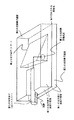
以下、本発明の実施形態を図面に基づいて説明する。図1乃至図3は本発明に係る複合光学素子の基本的な構成例を示す図である。図1乃至図3を参照して、本発明の各実施形態を説明する。なお、図1は斜視図、図2は正面図、図3は背面図である。
【0020】
(第1の実施形態)
本発明の第1の実施形態は、図1乃至図3に示すように、光と電気とを変換する第1の光学素子が形成された第1の光学素子基板と、第1の光学素子から出射する光、または、前記第1の光学素子に入射する光を整形する第2の光学素子が形成された第2の光学素子基板とを有する複合光学素子であって、前記第1の光学素子基板と前記第2の光学素子基板とを基板面同士を貼り合わせ、そのとき、前記第1の光学素子基板の側面と前記第2の光学素子基板の側面とが略同一平面上にあることを特徴としている。
【0021】
このような構成では、第1の光学素子と第2の光学素子との間で確実な貼り合わせ(接着)に必要な面積を確保し、かつ最小限無駄のない形状となる。これにより、不要な材料を使うことなく、最も少量の基板の大きさとなる。
【0022】
(第2の実施形態)
本発明の第2の実施形態は、上述した第1の実施形態の複合光学素子において、前記第1の光学素子は、面発光レーザーまたはフォトダイオードであることを特徴としている。
【0023】
面発光レーザーやフォトダイオードは、端面レーザーと異なり、その光軸が基板に対し垂直となる。また、第2の光学素子と接合し固定する面も光軸に垂直となる。これにより、この固定面を十分にとるように設計することが可能になる。端面レーザーでは、その固定面に当る発光面部分は非常に狭く、十分な固定は不可能である。
【0024】
(第3の実施形態)
本発明の第3の実施形態は、第1または第2の実施形態の複合光学素子において、第2の光学素子基板の表面に、第3の光学素子を固定するガイドが設けられていることを特徴としている。
【0025】
このように、第2の光学素子基板の表面に、第3の光学素子を固定するガイドを設けることで、第3の光学素子を低コストで(簡単な形で)高い位置精度に実装することが可能になる。
【0026】
(第4の実施形態)
本発明の第4の実施形態は、第1乃至第3のいずれかの実施形態の複合光学素子において、前記第2の光学素子は、ミラーであることを特徴としている。
【0027】
このように、第2の光学素子をミラーにすることで、第1の光学素子の光軸と異なる角度に第3の光学素子を実装することが可能になる。これにより、設計の自由度が増し、第3の光学素子を固定する面を大きく取ることが可能になる。
【0028】
(第5の実施形態)
本発明の第5の実施形態は、第4の実施形態の複合光学素子において、前記ミラーは、非球面であることを特徴としている。
【0029】
このように、第2の光学素子であるミラーを非球面にすることで、実装誤差に対する光結合効率への影響が小さい形状を設計できる。
【0030】
(第6の実施形態)
本発明の第6の実施形態は、第1乃至第5のいずれかの実施形態の複合光学素子において、前記第2の光学素子基板の上面には、第3の光学素子が固定され、第2の光学素子基板の下面には、第1の光学素子基板が固定されることを特徴としている。
【0031】
このような構成では、第1の光学素子の実装固定面と第3の光学素子の実装固定面がバッティングすることがなく、第2の光学素子は小型化が可能になり(第2の光学素子の面積をできるだけ小さくすることが可能となり)、部品コストを低減することができる。
【0032】
(第7の実施形態)
本発明の第7の実施形態は、第5乃至第6のいずれかの実施形態の複合光学素子において、前記ミラーの焦点に第1の光学素子と第3の光学素子が配置されていることを特徴としている。
【0033】
第5の実施形態のようにミラーは非球面であり、その焦点を最適に設計している。このミラーの焦点に第1の光学素子,第3の光学素子を設置することで、最適な光結合を実現できる(光結合器として、高い光結合効率を得ることができる)。
【0034】
(第8の実施形態)
本発明の第8の実施形態は、図4に示すように、第1乃至第7のいずれかの実施形態の複合光学素子において、前記第2の光学素子基板にスルーホールが設けられていることを特徴としている。
【0035】
この第8の実施形態では、第2の光学素子基板にスルーホールが設けられていることで、第1の光学素子である面発光レーザーやフォトダイオードなどの光学素子の電気接続が容易になる。これにより、第1の光学素子に裏面から電極をとるような無駄な加工をすることなく、複合光学素子を安価に製造することが可能になる。
【0036】
(第9の実施形態)
本発明の第9の実施形態は、図5に示すように、第1乃至第8のいずれかの実施形態の複合光学素子において、第1の光学素子と第3の光学素子との間に存在する光路部分に樹脂が封入されていることを特徴としている。
【0037】
このように、屈折率をコントロールした樹脂を封入することで、第3の光学素子表面での反射などを低減することができる。これにより、別途、第3の光学素子表面に反射防止膜などを加工することが不要になり、製造コストを低減できる。
【0038】
(第10の実施形態)
本発明の第10の実施形態は、図6に示すように、第1乃至第9のいずれかの実施形態の複合光学素子において、第1の光学素子基板および/または第2の光学素子基板には、これらが貼り合わされる基板面に接着剤を注入するための溝(注入溝)が設けられていることを特徴としている。
【0039】
接着溝以外の領域で、第1の光学素子基板と第2の光学素子基板とは当接しており、この領域において実装精度が決められている。このように、第10の実施形態では、接着剤を注入する溝を設けることで、第1の光学素子基板と第2の光学素子基板とが貼り合わされる基板面に接着剤が挟まれることがなくなり(接着剤の厚さによって実装誤差が生じるのを防止でき(実装精度の低下を防止でき))、かつ、固定する機能を得ることができる。
【0040】
(第11の実施形態)
本発明の第11の実施形態は、第1乃至第10のいずれかの実施形態の複合光学素子における第1の光学素子基板が平板状に配列された第1の光学素子部品と、第1乃至第10のいずれかの実施形態の複合光学素子における第2の光学素子基板が平板状に配列された第2の光学素子部品とが貼り合わされていることを特徴とする複合光学部品である。すなわち、第1の光学素子が面発光レーザーやフォトダイオードである場合には、複数の第1の光学素子(基板)を平板状に配列することが可能である。
【0041】
具体的には、第10の実施形態に示すように第1乃至第9のいずれかの実施形態の複合光学素子において、第1の光学素子基板および/または第2の光学素子基板には、これらが貼り合わされる基板面に接着剤を注入するための溝(注入溝)が設けられている場合に、注入溝に接着剤を注入する。この工程を、ウェハー毎に行なう。接着剤の注入は毛細管現象を利用する事により、大きなウェハーの状態で可能である。接着剤の注入をウェハーごとに行なう事で、接着剤の注入を1つの素子毎に行なう場合に比べて、遥かに多くの素子を一度に作製することができる。この後に、第1の光学素子基板と第2の光学素子基板とを同時にダイシングし、それぞれの複合光学素子に切り分けることができる。これにより、製造コストを遥かに小さくすることができる。
【0042】
(第12の実施形態)
本発明の第12の実施形態は、図7(a)乃至(c)に概略を示すように、第1の光学素子基板が平板状に配列された状態の第1の光学素子部品を作製する工程と、第2の光学素子基板が平板状に配列された状態の第2の光学素子部品を作製する工程と、第1の光学素子部品と第2の光学素子部品とを貼り合わせて、複合光学素子が平板状に配列された状態の複合光学部品とする工程と、複合光学部品において平板状に配列している個々の複合光学素子を分離する工程とを有していることを特徴としている。
【0043】
図7(a)乃至(c)に示すように、複数の素子を一括して同時に加工することにより、1つ1つの実装コストを大幅に低減できる。通常、半導体プロセスを用いる第1の光学素子や第2の光学素子は、ウェハー状に加工される。そのため、一般的に作製される第1,第2の光学素子は平板状に作成される。このため、平板状に配列して、加工することでのコスト高にはならない。
【0044】
(第13の実施形態)
本発明の第13の実施形態は、光と電気とを変換する第1の光学素子が形成された第1の光学素子基板と、前記第1の光学素子から出射する光、または、前記第1の光学素子に入射する光を整形する第2の光学素子が形成された第2の光学素子基板とを有する複合光学素子を基体に実装する工程と、基体に実装した複合光学素子に第3の光学素子を実装する工程とを有していることを特徴としている。
【0045】
ここで、基体とは、サブマウントやステム,プリント基板といったものである。この第13の実施形態では、第1の光学素子基板と第2の光学素子基板とを接合した複合光学素子をサブマウントなどの基体に実装する。この複合光学素子は、サブmmのオーダーと小型であるため、微調整が効き、高精度の実装が可能である。この状態であれば、LSIの接合,ワイヤーボンディングなどの電気接合などを行なうことも可能である。光ファイバーなどの大きな光学素子を一体化している場合には、このようなことは不可能である。全ての実装を終えた最後に、第3の光学素子を実装する。これは、第6の実施形態に示したように、第2の光学素子基板の下面に第1の光学素子基板を接合し、上面に第3の光学素子を実装するレイアウトで実現できる。
【0046】
【実施例】
次に、本発明の実施例を説明する。
【0047】
(実施例1)
実施例1のデバイスは、図8に示すように、面発光レーザーが形成された第1の光学素子基板と第2の光学素子として曲面ミラーが形成された第2の光学素子基板(オプティカルベンチ)と第3の光学素子としての光ファイバーからなる光学系とを備えた複合光学素子と、LSIと前記複合光学素子とが実装されているサブマウントと、サブマウントを固定しているプリント基板とからなっている。
【0048】
ここで、第2の光学素子基板(オプティカルベンチ)には、曲面ミラーの光軸上に光ファイバー固定ガイド(V溝)が設けられている。また、第2の光学素子基板と第1の光学素子基板とは、それぞれの側面(4つの側面)が同一平面上にあるように構成されている。また、曲面ミラーは、その表面が非球面の形状となっており、曲面ミラーの焦点は、第1の光学素子(面発光レーザー)と光ファイバーの端面とに合わされている。そして、曲面ミラーの非球面形状は、それぞれの焦点が合い、かつ、実装精度がある程度低下した場合にも、その結合効率がそれほど低下しないように設計されている。
【0049】
この実施例1のデバイスは、次のように作製される。なお、第1の光学素子である面発光レーザーは、GaInNAs系の材料で、その波長は1.3μm帯となっている。第1の光学素子である面発光レーザーは、4インチの大きさ(例えば直径)のウェハー上に配列された状態で作製される。その配列位置は、第2の光学素子と合わせて設計されている。
【0050】
また、第2の光学素子基板(オプティカルベンチ)には、4インチの大きさ(例えば直径)、厚さ0.5mmのSiウェハーを用いた。そして、第2の光学素子基板に、フォトリソプロセスとエッチングプロセスを併用して、任意立体形状を作りこむ。初めに、第2の光学素子基板の一方の面(表面)に光ファイバー用のガイド機構を加工する。ガイド機構は光ファイバーを精度良く固定する機構であれば良く、その形状は、V型,U型など、どのような形状でも良い。いまの例では、フォトリソプロセスによってマスクを加工し、異方性エッチングを利用したV溝をガイド機構として形成した。次に、第2の光学素子基板の他方の面(裏面)にミラー面を作りこむ。このミラー面を、先ほどのV溝と同様に、フォトリソによるレジストマスク加工と異方性エッチングによって作る。異方性エッチングではその角度が制限されるために、45°に加工することは難しい。一度異方性エッチングで作製されたミラーを再度、フォトリソプロセスによって、45°でかつ非球面に仕上げる。この時には、一般的なマスクではなく、グレースケールマスクを用いた。
【0051】
グレースケールマスク方法では、フォトリソグラフィーに用いるマスクを、透過率が1と0の細かいドットによって階調表現したものや中間調によって表現されたものがある。階調表現によって、明るい部分,暗い部分ができ、これをフォトレジストに露光する事で、暗い所は高く、明るい所は低く(ポジレジストの場合)、中間高さを含む、高さ表現されたレジスト形状を得ることができる。このようにマスク形状を工夫する事で、レジストを3次元的かつ任意形状に加工する事ができる(グレースケールマスクの作製方法の詳細は特開平11−177123,特開2000−280366などに示されている)。
【0052】
このグレースケールマスクを利用することで、45°のミラー表面を非球面形状に加工することができる。異方性エッチングによって傾斜面を作製し、その表面にスプレーコーターによって、レジストを塗布する。レジストは表面に凹凸があろうとも、ほぼ均一に膜厚が制御されている。この膜に先ほどのグレースケールマスクを用いて、傾斜面に塗布されたレジストに露光する。これを現像することで、設計された非球面の形状を作りこむ。このレジストをドライエッチングによって、基板に転写する。非球面形状は実装した時の誤差による結合効率の低下を緩和するように設計されている。特に、非球面にすることで、そのビームウエストが光ファイバーの直径に小さくなる領域をできるだけ大きくなるように設計されている。これにより、光軸に水平方向の誤差には、影響が小さい光学系となっている。
【0053】
この曲面ミラーを加工したSiウェハー(第2の光学素子部品)と面発光レーザーを作りこんだウェハー(第1の光学素子部品)とを貼り合わせる(図7(b)を参照)。貼り合わせには、図7(a)に示されているように、第1の光学素子部品と第2の光学素子部品の一部に作られているアライメントマークを合わせるように位置合わせをする。位置合わせには顕微鏡観察し、微動ができる装置を利用する。アライメントマークは、それぞれのフォトリソプロセスにおいて同時に作られているため、その位置精度は高い。また、接着剤は、貼り合わせる前に、第2の光学素子部品の表面に塗布されている。この第1の光学素子部品と第2の光学素子部品とを貼り合わせたウェハーをダイシング装置で個別の複合光学素子に分離する(図7(c)を参照)。ダイシングは2枚同時に行なう。複合光学素子単体はそれぞれ、接着剤によって貼り合わされている。これにより、図1乃至図3に示すような側面(4つの側面)が略同一平面上にある複合光学素子を得ることができる。
【0054】
そして、この複合光学素子を、図8に示すように、サブマウントに実装する。サブマウントには、複合光学素子以外にも、面発光レーザーを駆動するLSIやその配線などが作りこまれている。この複合光学素子とサブマウントの実装は、電気的な接合ができれば良く、その精度は高いものを要求されない。
【0055】
実施例1では、面発光レーザーやLSIは一般的なバンプによる実装とした。実施例1で用いた面発光レーザーは、両極の電極を裏面から取れるように、基板にスルーホールを作りこんである。
【0056】
複合光学素子やLSIが実装されたサブマウントは、プリント基板に実装される。実装は一般的な半田で良い。この場合には、複合光学素子部にはポリイミドなどの樹脂による保護膜を付けておく。これにより、半田による汚染を防止できる。また、第1の光学素子基板と第2の光学素子基板との貼り合わせ(接合)に用いた接着剤は、半田による高温プロセスに耐えうるものを採用している。
【0057】
そして、複合光学素子のサブマウントが実装されたプリント基板には、光ファイバー用のスペーサーを作りこむ。これは、光ファイバーを単に固定する機能を有しているだけであり、実装精度を上げる機能はない。このスペーサーに光ファイバーの一部を固定すると同時に、複合光学素子に設けられているV溝に光ファイバーの端部を設置する。V溝は光ファイバーの形状に合わせて設計されており、正確に実装されることで、光損失はほとんどない。V溝は、上から光ファイバーをあてがうだけで、正確な位置に誘導する機能を持つ。光ファイバーにおける光軸方向の実装精度は、光ファイバーを複合光学素子に当接することで、高い精度を有している。
【0058】
(実施例2)
実施例2のデバイスは、図5,図8に示すように、面発光レーザーが形成された第1の光学素子基板と第2の光学素子としての曲面ミラーが形成された第2の光学素子基板(オプティカルベンチ)と第3の光学素子としての光ファイバーからなる光学系とを備えた複合光学素子と、LSIと第2の光学素子基板(オプティカルベンチ)とが実装されているサブマウントと、サブマウントを固定しているプリント基板とからなっている。
【0059】
ここで、第2の光学素子基板(オプティカルベンチ)には、曲面ミラーの光軸上に光ファイバー固定ガイド(V溝)が設けられている。また、第2の光学素子基板(オプティカルベンチ)には、図5に示すように、電極配線用のスルーホールが設けられている。このスルーホールの上方からワイヤーボンディングで電気的に面発光レーザーは接続されている。また、第2の光学素子基板と第1の光学素子基板とは、それぞれの側面(4つの側面)が同一平面上にあるように構成されている。また、曲面ミラーは、その表面が非球面の形状となっており、曲面ミラーの焦点は、第1の光学素子(面発光レーザー)と光ファイバーの端面とに合わされている。そして、曲面ミラーの非球面形状は、それぞれの焦点が合い、かつ、実装精度がある程度低下した場合にもその結合効率がそれほど低下しないように設計されている。また、この実施例2では、図5に示されているように、面発光レーザーから光ファイバーまでの光路部分に透明な樹脂が封入されている。これにより、不要な反射光も抑えることができ、ノイズを低減できる。
【0060】
この実施例2のデバイスは、次のように作製される。なお、第1の光学素子である面発光レーザーは、GaInNAs系の材料で、その波長は1.3μm帯となっている。第1の光学素子である面発光レーザーは、4インチの大きさ(例えば直径)のウェハー上に配列された状態で作製される。その配列位置は、第2の光学素子と合わせて設計されている。
【0061】
また、第2の光学素子基板(オプティカルベンチ)には、4インチの大きさ(例えば直径)、厚さ0.5mmのSiウェハーを用いた。そして、第2の光学素子基板に、フォトリソプロセスとエッチングプロセスを併用して、任意立体形状を作りこむ。初めに、第2の光学素子基板の一方の面(表面)に光ファイバー用のガイド機構を加工する。ガイド機構は光ファイバーを精度良く固定する機構であれば良く、その形状は、V型,U型など、どのような形状でも良い。いまの例では、フォトリソプロセスによってマスクを加工し、異方性エッチングを利用したV溝をガイド機構として形成した。次に、第2の光学素子基板の他方の面(裏面)にミラー面を作りこむ。このミラー面を、先ほどのV溝と同様に、フォトリソによるレジストマスク加工と異方性エッチングによって作る。異方性エッチングではその角度が制限されるために、45°に加工することは難しい。一度異方性エッチングで作製されたミラーを再度、フォトリソプロセスによって、45°でかつ非球面に仕上げる。この時には、一般的なマスクではなく、グレースケールマスクを用いた。
【0062】
このグレースケールマスクを利用することで、45°のミラー表面を非球面形状に加工することができる。異方性エッチングによって傾斜面を作製し、その表面にスプレーコーターによって、レジストを塗布する。レジストは表面に凹凸があろうとも、ほぼ均一に膜厚が制御されている。この膜に先ほどのグレースケールマスクを用いて、傾斜面に塗布されたレジストに露光する。これを現像することで、設計された非球面の形状を作りこむ。このレジストをドライエッチングによって、基板に転写する。非球面形状は実装した時の誤差による結合効率の低下を緩和するように設計されている。特に、非球面にすることで、そのビームウエストが光ファイバーの直径に小さくなる領域をできるだけ大きくなるように設計されている。これにより、光軸に水平方向の誤差には、影響が小さい光学系となっている。
【0063】
この曲面ミラーを加工したSiウェハー(第2の光学素子部品)と面発光レーザーを作りこんだウェハー(第1の光学素子部品)とを貼り合わせる(図7(b)を参照)。貼り合わせには、図7(a)に示されているように、第1の光学素子部品と第2の光学素子部品の一部に作られているアライメントマークを合わせるように位置合わせをする。位置合わせには顕微鏡観察し、微動ができる装置を利用する。アライメントマークは、それぞれのフォトリソプロセスにおいて同時に作られているため、その位置精度は高い。また、接着剤は、貼り合わせる前に、第2の光学素子部品の表面に塗布されている。この第1の光学素子部品と第2の光学素子部品とを貼り合わせたウェハーをダイシング装置で個別の複合光学素子に分離する(図7(c)を参照)。ダイシングは2枚同時に行なう。複合光学素子単体はそれぞれ、接着剤によって貼り合わされている。これにより、図1乃至図3に示すような側面(4つの側面)が略同一平面上にある複合光学素子を得ることができる。
【0064】
そして、この複合光学素子を、図8に示すように、サブマウントに実装する。サブマウントには、複合光学素子以外にも、面発光レーザーを駆動するLSIやその配線などが作りこまれている。この複合光学素子とサブマウントの実装は、電気的な接合ができれば良く、その精度は高いものを要求されない。
【0065】
実施例2では、面発光レーザーやLSIは一般的なワイヤーボンディングとした。面発光レーザーは、裏面をグラウンド(接地レベル)として、表面に信号(シグナル)をとる電極を備えている。グラウンド(接地)はサブマウントにバンプやハンダによって直接接合されている。また、面発光レーザーの表面の電極は、第2の光学素子基板に設けたスルーホールを利用して接続される。なお、スルーホールは、単なる穴で良く、表面に光ファイバー用のV溝を作る時と、ミラーを作る裏面への加工の時に、スルーホール用にマスクを設計しておく。これにより、第2の光学素子の基板には電極用のスルーホールが設けられ、電極を取ることができる。
【0066】
複合光学素子やLSIが実装されたサブマウントは、プリント基板に実装される。実装は一般的な半田で良い。この場合には、複合光学素子部にはポリイミドなどの樹脂による保護膜を付けておく。これにより、半田による汚染を防止できる。また、第1の光学素子基板と第2の光学素子基板との貼り合わせ(接合)に用いた接着剤は、半田による高温プロセスに耐えうるものを採用している。
【0067】
そして、図5に示すように、第1の光学素子と第3の光学素子との間に存在する光路部分に透明な樹脂を封入する。樹脂には、熱硬化型のものを利用し、屈折率がコントロールされている。この樹脂の硬化は、光ファイバ−を設置した後に熱を加える事で行なう。
【0068】
そして、複合光学素子のサブマウントが実装されたプリント基板には、光ファイバー用のスペーサーを作りこむ。これは、光ファイバーを単に固定する機能を有しているだけであり、実装精度を上げる機能はない。このスペーサーに光ファイバーの一部を固定すると同時に、複合光学素子に設けられているV溝に光ファイバーの端部を設置する。V溝は光ファイバーの形状に合わせて設計されており、正確に実装されることで、光損失はほとんどない。V溝は、上からファイバーをあてがうだけで,正確な位置に誘導する機能を持つ。光ファイバーにおける光軸方向の実装精度は、光ファイバーを複合光学素子に当接することで、高い精度を有している。
【0069】
(実施例3)
実施例3のデバイスは、図6,図8に示すように、フォトダイオードが形成された第1の光学素子基板と第2の光学素子としての曲面ミラーが形成された第2の光学素子基板(オプティカルベンチ)と第3の光学素子としての光ファイバーからなる光学系とを備えた複合光学素子と、LSIと第2の光学素子基板(オプティカルベンチ)とが実装されているサブマウントと、サブマウントを固定しているプリント基板とからなっている。
【0070】
ここで、第2の光学素子基板(オプティカルベンチ)には、曲面ミラーの光軸上に光ファイバー固定ガイド(V溝)が設けられている。また、第2の光学素子基板と第1の光学素子基板とは、それぞれの側面(4つの側面)が同一平面上にあるように構成されている。曲面ミラーは、その表面が非球面の形状となっており、曲面ミラーの焦点は、第1の光学素子(フォトダイオード)と光ファイバーの端面とに合わされている。そして、曲面ミラーの非球面形状は、それぞれの焦点が合い、かつ、実装精度がある程度低下した場合にも、その結合効率がそれほど低下しないように設計されている。また、この実施例3では、第2の光学素子基板に接着剤の注入溝が設けられている。この注入溝の部分に接着剤が注入されることで、第2の光学素子基板は第1の光学素子基板と接合固定されるようになっている。
【0071】
この実施例3のデバイスは、次のように作製される。第1の光学素子であるフォトダイオードは、Siによって作製され、4インチの大きさ(例えば直径)のウェハー上に配列された状態で作製される。その配列位置は、第2の光学素子と合わせて設計されている。
【0072】
また、第2の光学素子基板(オプティカルベンチ)には、4インチの大きさ(例えば直径)、厚さ0.5mmのSiウェハーを用いた。そして、第2の光学素子基板に、フォトリソプロセスとエッチングプロセスを併用して、任意立体形状を作りこむ。初めに、第2の光学素子基板の一方の面(表面)に光ファイバー用のガイド機構を加工する。ガイド機構は光ファイバーを精度良く固定する機構であれば良く、その形状は、V型,U型など、どのような形状でも良い。いまの例では、フォトリソプロセスによってマスクを加工し、異方性エッチングを利用したV溝をガイド機構として形成した。次に、第2の光学素子基板の他方の面(裏面)にミラー面を作りこむ。このミラー面を、先ほどのV溝と同様に、フォトリソによるレジストマスク加工と異方性エッチングによって作る。異方性エッチングではその角度が制限されるために、45°に加工することは難しい。一度異方性エッチングで作製されたミラーを再度、フォトリソプロセスによって、45°でかつ非球面に仕上げる。この時には、一般的なマスクではなく、グレースケールマスクを用いた。
【0073】
このグレースケールマスクを利用することで、45°のミラー表面を非球面形状に加工することができる。異方性エッチングによって傾斜面を作製し、その表面にスプレーコーターによって、レジストを塗布する。レジストは表面に凹凸があろうとも、ほぼ均一に膜厚が制御されている。この膜に先ほどのグレースケールマスクを用いて、傾斜面に塗布されたレジストに露光する。これを現像することで、設計された非球面の形状を作りこむ。このレジストをドライエッチングによって、基板に転写する。非球面形状は実装した時の誤差による結合効率の低下を緩和するように設計されている。特に、非球面にすることで、そのビームウエストが光ファイバーの直径に小さくなる領域をできるだけ大きくなるように設計されている。これにより、光軸に水平方向の誤差には、影響が小さい光学系となっている。
【0074】
この曲面ミラーを加工したSiウェハー(第2の光学素子部品)とフォトダイオードを作りこんだウェハー(第1の光学素子部品)とを貼り合わせる(図7(b)を参照)。貼り合わせには、図7(a)に示されているように、第1の光学素子部品と第2の光学素子部品の一部に作られているアライメントマークを合わせるように位置合わせをする。位置合わせには顕微鏡観察し、微動ができる装置を利用する。アライメントマークは、それぞれのフォトリソプロセスにおいて同時に作られているため、その位置精度は高い。また、第2の光学素子部品である曲面ミラーが作りこまれたSiウェハーには接着剤が流し込まれる溝(注入溝)が作られている。この溝は、流路のように作られ、接着剤を一方向から流しこむことで、全体に広がるように作られている。
【0075】
この第1の光学素子部品と第2の光学素子部品とを貼り合わせたウェハーをダイシング装置で個別の複合光学素子に分離する(図7(c)を参照)。ダイシングは2枚同時に行なう。先の接着剤により、複合光学素子単体はそれぞれ、接着剤によって貼り合わされている。これにより、図1乃至図3に示すような側面(4つの側面)が略同一平面上にある複合光学素子を得ることができる。
【0076】
そして、この複合光学素子を、図8に示すように、サブマウントに実装する。サブマウントには、複合光学素子以外にも、フォトダイオードを駆動するLSIやその配線などが作りこまれている。この複合光学素子とサブマウントの実装は、電気的な接合ができれば良く、その精度は高いものを要求されない。実施例3では、フォトダイオードやLSIは一般的なバンプによる実装とした。実施例3で用いたフォトダイオードは、両極の電極を裏面から取れるように、基板にスルーホールを作りこんである。
【0077】
複合光学素子やLSIが実装されたサブマウントは、プリント基板に実装される。実装は一般的な半田で良い。この場合には、複合光学素子部にはポリイミドなどの樹脂による保護膜を付けておく。これにより、半田による汚染を防止できる。また、第1の光学素子基板と第2の光学素子基板との貼り合わせ(接合)に用いた接着剤は、半田による高温プロセスに耐えうるものを採用している。
【0078】
そして、複合光学素子のサブマウントが実装されたプリント基板には、光ファイバー用のスペーサーを作りこむ。これは、光ファイバーを単に固定する機能を有しているだけであり、実装精度を上げる機能はない。このスペーサーに光ファイバーの一部を固定すると同時に、複合光学素子に設けられているV溝に光ファイバーの端部を設置する。V溝は光ファイバーの形状に合わせて設計されており、正確に実装されることで、光損失はほとんどない。V溝は、上から光ファイバーをあてがうだけで,正確な位置に誘導する機能を持つ。光ファイバーにおける光軸方向の実装精度は、光ファイバーを複合光学素子に当接することで、高い精度を有している。
【0079】
(実施例4)
実施例4のデバイスは、図9,図10に示すように、面発光レーザーが形成された第1の光学素子基板と第2の光学素子としてのマイクロレンズが形成された第2の光学素子基板(オプティカルベンチ)と第3の光学素子としての光ファイバーからなる光学系とを備えた複合光学素子と、LSIと第2の光学素子基板(オプティカルベンチ)とが実装されているサブマウントと、サブマウントを固定しているプリント基板とからなっている。
【0080】
ここで、第2の光学素子基板(オプティカルベンチ)には、マイクロレンズの光軸上に光ファイバー固定ガイドが設けられている。また、第2の光学素子基板(オプティカルベンチ)と第1の光学素子基板とは、それぞれの側面(4つの側面)が同一平面上にあるように構成されている。マイクロレンズは、その表面が非球面の形状となっており、マイクロレンズの焦点は、第1の光学素子(面発光レーザー)と光ファイバーの端面とに合わされている。そして、マイクロレンズの非球面形状は、それぞれの焦点が合い、かつ、実装精度がある程度低下した場合にもその結合効率がそれほど低下しないように設計されている。また、この実施例4では、第2の光学素子基板に接着剤の注入溝が設けられている。この注入溝の部分に接着剤が注入されることで、第2の光学素子基板は第1の光学素子基板と接合固定されるようになっている。
【0081】
この実施例4のデバイスは、次のように作製される。なお、第1の光学素子である面発光レーザーは、GaInNAs系の材料で、その波長は1.3μm帯となっている。第1の光学素子である面発光レーザーは、4インチの大きさ(例えば直径)のウェハー上に配列された状態で作製される。その配列位置は、第2の光学素子と合わせて設計されている。
【0082】
また、第2の光学素子基板(オプティカルベンチ)には、4インチの大きさ(例えば直径)、厚さ0.5mmの石英ウェハーを用いた。そして、第2の光学素子基板に、フォトリソプロセスとエッチングプロセスを併用して、任意立体形状を作りこむ。初めに、第2の光学素子基板の一方の面(表面)に光ファイバー用のガイド機構を加工する。ガイド機構は光ファイバーを精度良く固定する機構であれば良く、その形状は、V型,U型など、どのような形状でも良い。いまの例では、フォトリソプロセスによってマスクを加工し、ドライエッチングを利用してガイド機構を形成した。次に、第2の光学素子基板の他方の面(裏面)にマイクロレンズ面を作りこむ。このマイクロレンズ面を、先ほどのガイド機構と同様に、フォトリソによるレジストマスク加工とドライエッチングによって作る。この時には、一般的なマスクではなく、グレースケールマスクを用いた。マイクロレンズは非球面形状であり、これは実装した時の誤差による結合効率の低下を緩和するように設計されている。特に、非球面にすることで、そのビームウエストが光ファイバーの直径に小さくなる領域をできるだけ大きくなるように設計してある。これにより、光軸に水平方向の誤差には、影響が小さい光学系となっている。
【0083】
そして、このマイクロレンズを加工した石英ウェハー(第2の光学素子部品)と面発光レーザーを作りこんだウェハー(第1の光学素子部品)とを貼り合わせる(図7(b)を参照)。貼り合わせには、図7(a)に示されているように、第1の光学素子部品と第2の光学素子部品の一部に作られているアライメントマークを合わせるように位置合わせをする。位置合わせには顕微鏡観察し、微動ができる装置を利用する。アライメントマークは、それぞれのフォトリソプロセスにおいて同時に作られているため、その位置精度は高い。また、マイクロレンズが作りこまれた第2の光学素子部品である石英ウェハーには、接着剤が流し込まれる溝(注入溝)が作られている。この溝は、流路のように作られ、接着剤を一方向から流しこむことで、全体に広がるように作られている。
【0084】
この第1の光学素子部品と第2の光学素子部品とを貼り合わせたウェハーをダイシング装置で個別の複合光学素子に分離する(図7(c)を参照)。ダイシングは2枚同時に行なう。先の接着剤により、複合光学素子単体はそれぞれ、接着剤によって貼り合わされている。これにより、図1乃至図3に示すような側面(4つの側面)が略同一平面上にある複合光学素子を得ることができる。
【0085】
そして、この複合光学素子を、図10に示すように、サブマウントに実装する。サブマウントには、複合光学素子以外にも、面発光レーザーを駆動するLSIやその配線などが作りこまれている。この複合光学素子とサブマウントの実装は、電気的な接合ができれば良く、その精度は高いものを要求されない。実施例4では、面発光レーザーやLSIは一般的なワイヤーボンディングとした。面発光レーザーは裏面をグラウンドとして、表面に信号(シグナル)をとる電極を備えている。グラウンドはサブマウントにバンプやハンダによって直接接合されている。また、面発光レーザーの表面の電極は、第2の光学素子基板に設けたスルーホールを利用して接続される。なお、スルーホールは、単なる穴で良く、表面に光ファイバー用のV溝を作る時と、ミラーを作る裏面への加工の時に、スルーホール用にマスクを設計しておく。これにより、第2の光学素子基板には電極用のスルーホールが設けられ、電極を取ることができる。
【0086】
複合光学素子やLSIが実装されたサブマウントは、プリント基板に実装される。実装は一般的な半田で良い。この場合には、複合光学素子部にはポリイミドなどの樹脂による保護膜を付けておく。これにより、半田による汚染を防止できる。また、第1の光学素子基板と第2の光学素子基板との貼り合わせ(接合)に用いた接着剤は、半田による高温プロセスに耐えうるものを採用している。
【0087】
そして、複合光学素子のサブマウントが実装されたプリント基板には、光ファイバー用のスペーサーを作りこむ。これは、光ファイバーを単に固定する機能を有しているだけであり、実装精度を上げる機能はない。このスペーサーに光ファイバーの一部を固定すると同時に、複合光学素子に設けられているV溝に光ファイバーの端部を設置する。V溝は光ファイバーの形状に合わせて設計されており、正確に実装されることで、光損失はほとんどない。V溝は上からファイバーをあてがうだけで,正確な位置に誘導する機能を持つ。光ファイバーにおける光軸方向の実装精度は、光ファイバーを複合光学素子に当接することで、高い精度を有している。
【0088】
【発明の効果】
以上に説明したように、請求項1乃至請求項9記載の発明によれば、光と電気とを変換する第1の光学素子が作りこまれた第1の光学素子基板と、
前記第1の光学素子から出射する光、または、前記第1の光学素子に入射する光を整形する第2の光学素子が作りこまれた第2の光学素子基板と、
前記第2の光学素子との間で光の導波を行う第3の光学素子とを有する複合光学素子であって、
前記第3の光学素子は、前記第2の光学素子基板の上面に固定され、前記第2の光学素子基板の下面には、前記第1の光学素子基板が固定されており、
前記第1の光学素子基板の側面と前記第2の光学素子基板の側面とが略同一平面上になるように、前記第1の光学素子基板と前記第2の光学素子基板とが基板面同士で貼り合わされているので、無駄な材料を使うことなく、面発光レーザやフォトダイオードなどの第1の光学素子とミラーなどの第2の光学素子とを低コストで高精度に実装することが可能になる。また、第3の光学素子は、前記第2の光学素子基板の上面に固定され、前記第2の光学素子基板の下面には、前記第1の光学素子基板が固定されるので、第1の光学素子の実装固定面と第3の光学素子の実装固定面がバッティングすることがなく、第2の光学素子は小型化が可能になり(第2の光学素子の面積をできるだけ小さくすることが可能となり)、部品コストを低減することができる。
【0089】
特に、請求項2記載の発明では、第1の光学素子として、面発光レーザーやフォトダイオードような光軸と垂直に平面状の素子を用いることで、固定する面が大きくとれ、十分な固定強度を得ることができる。これにより、一般的な接着剤による固定が可能になり、低コストの製造が可能になる。
【0090】
また、請求項3記載の発明では、第2の光学素子基板に第3の光学素子を固定するガイドを設けたことにより、第3の光学素子を簡便に高い位置精度に誘導でき、これにより、低コストの実装が可能になる。
【0091】
また、請求項4記載の発明では、第2の光学素子をミラーとすることで、第3の光学素子を安定して固定できるようにレイアウトを作ることができる。これにより、第3の光学素子を特殊な固定方法を採用する必要がなく製造工程がシンプルになり、低コストで実装が可能になる。
【0092】
また、請求項5記載の発明では、第2の光学素子のミラー面を非球面にすることで、より高い光結合効率を得ることができる。また、形状を最適化することで、実装誤差に大きな影響を受けない光結合効率を実現できる複合光学素子を提供できる。
【0094】
また、請求項6記載の発明では、第2の光学素子の焦点位置に第1の光学素子と第3の光学素子を配置することで、それぞれ高い光結合効率を得る事ができる。
【0095】
また、請求項7記載の発明では、第2の光学素子基板にスルーホールを設けることで、簡便に電気接続が可能になり、低コストでの実装が可能になる。
【0096】
また、請求項8記載の発明では、第1の光学素子と第3の光学素子の間における光路部分に樹脂が封入されているので、第3の光学素子の表面に反射防止膜などを加工することが不要になり、製造コストを低減できる。
【0097】
また、請求項9記載の発明では、第1の光学素子基板と第2の光学素子基板とが貼り合わされる基板面に接着剤を注入するための溝を設けているので、接着剤が第1の光学素子基板と第2の光学素子基板との当接部分に挟まれることなく、実装精度の低下を防止できる。
【0098】
また、請求項10記載の発明によれば、請求項1乃至請求項9のいずれか一項に記載の複合光学素子における第1の光学素子基板が平板状に配列された第1の光学素子部品と、請求項1乃至請求項9のいずれか一項に記載の複合光学素子における第2の光学素子基板が平板状に配列された第2の光学素子部品とが貼り合わされており、第1の光学素子と第2の光学素子との実装をウェハーごと行なう事で、複合光学素子を1つ1つ実装する場合に比べ、遥かに製造コストが小さくなる。
【図面の簡単な説明】
【図1】本発明に係る複合光学素子の基本的な構成例を示す図である。
【図2】本発明に係る複合光学素子の基本的な構成例を示す図である。
【図3】本発明に係る複合光学素子の基本的な構成例を示す図である。
【図4】第2の光学素子基板にスルーホールが設けられている複合光学素子を示す図である。
【図5】第1の光学素子と第3の光学素子との間に存在する光路部分に樹脂が封入されている複合光学素子を示す図である。
【図6】第1の光学素子基板および/または第2の光学素子基板には、これらが貼り合わされる基板面に接着剤を注入するための溝(注入溝)が設けられている複合光学素子を示す図である。
【図7】本発明に係る複合光学素子の製造工程例を示す図である。
【図8】本発明の実施例を説明するための図である。
【図9】本発明の実施例を説明するための図である。
【図10】本発明の実施例を説明するための図である。[0001]
BACKGROUND OF THE INVENTION
The present invention relates to a composite optical element and a composite optical unitTo goodsRelated.
[0002]
[Prior art]
Surface-emitting lasers and photodiodes are increasingly useful as key devices for parallel optical interconnection. In its practical use, mounting for controlling light is required, and higher mounting accuracy is required compared to mounting of conventional electrical components. Such high-accuracy mounting increases the manufacturing cost and hinders the spread to the market.
[0003]
In view of this, a technique has been studied in which a member processed with extremely high precision using a semiconductor process or the like is used, and an optical element is mounted on the surface of the member as a reference surface. This high-precision processed member is called an optical bench, and is a very important technique for satisfying various requirements as a mounting technique using an optical bench. According to this technology, high-accuracy components can be produced at low cost, and mounting using these components can be performed with high accuracy and at low cost. At present, it plays a major role in optical fiber mounting. I'm in charge.
[0004]
However, even in such a mounting technique, the optical fiber and the end face laser are merely optically coupled, and there are still problems in terms of versatility and manufacturing cost. In particular, optical coupling between a surface emitting laser and an optical fiber or a waveguide is one of the biggest problems. A surface emitting laser or a photodiode has a light emitting surface and a light receiving surface that are perpendicular to the substrate, and is greatly different from the conventional end surface laser. In response to the problem of this surface emitting laser, there is one that provides a similar optical bench through a mirror inclined at 45 °. This makes it possible to mount the surface emitting laser with high accuracy, but still has problems in terms of manufacturing cost.
[0005]
[Problems to be solved by the invention]
The present invention relates to a composite optical element and a composite optical unit capable of mounting a first optical element such as a surface emitting laser and a photodiode and a second optical element such as a mirror with high accuracy at low cost.GoodsIt is intended to provide.
[0006]
[Means for Solving the Problems]
In order to achieve the above object, the invention according to claim 1A first optical element substrate on which a first optical element for converting light and electricity is formed;
A second optical element substrate on which a second optical element for shaping light emitted from the first optical element or light incident on the first optical element is formed;
A composite optical element having a third optical element for guiding light to and from the second optical element,
The third optical element is fixed to the upper surface of the second optical element substrate, and the first optical element substrate is fixed to the lower surface of the second optical element substrate,
The first optical element substrate and the second optical element substrate are arranged so that the side surface of the first optical element substrate and the side surface of the second optical element substrate are substantially flush with each other. Are pasted togetherIt is characterized by that.
[0007]
According to a second aspect of the present invention, in the composite optical element according to the first aspect, the first optical element is a surface emitting laser or a photodiode.
[0008]
According to a third aspect of the present invention, in the composite optical element according to the first or second aspect, a guide for fixing the third optical element is provided on the surface of the second optical element substrate. It is characterized by.
[0009]
According to a fourth aspect of the present invention, in the composite optical element according to any one of the first to third aspects, the second optical element is a mirror.
[0010]
The invention according to claim 5 is the composite optical element according to claim 4, wherein the mirror is an aspherical surface.
[0012]
Also,Claim 6The described invention is claimed.5The composite optical element described above is characterized in that a first optical element and a third optical element are arranged at the focal point of the mirror.
[0013]
Also,Claim 7The invention described in claims 1 toClaim 6In the composite optical element according to any one of the above, a through hole is provided in the second optical element substrate.
[0014]
Also,Claim 8The invention described in claims 1 toClaim 7The composite optical element according to any one of the above is characterized in that a resin is sealed in an optical path portion existing between the first optical element and the third optical element.
[0015]
Also,Claim 9The invention described in claims 1 toClaim 8In the composite optical element according to any one of the above, the first optical element substrate and / or the second optical element substrate is provided with a groove for injecting an adhesive into the substrate surface to which these are bonded. It is characterized by having.
[0016]
Also,Claim 10The invention described in claims 1 toClaim 9The first optical element component in which the first optical element substrate in the composite optical element according to claim 1 is arranged in a flat plate shape; andClaim 9The composite optical element according to any one of the above, wherein the second optical element substrate in which the second optical element substrate is arranged in a flat plate shape is bonded together.
[0019]
DETAILED DESCRIPTION OF THE INVENTION
Hereinafter, embodiments of the present invention will be described with reference to the drawings. 1 to 3 are views showing a basic configuration example of a composite optical element according to the present invention. Each embodiment of the present invention will be described with reference to FIGS. 1 is a perspective view, FIG. 2 is a front view, and FIG. 3 is a rear view.
[0020]
(First embodiment)
As shown in FIGS. 1 to 3, the first embodiment of the present invention includes a first optical element substrate on which a first optical element that converts light and electricity is formed, and a first optical element. A first optical element comprising: a second optical element substrate on which a second optical element for shaping emitted light or light incident on the first optical element is formed; The substrate surfaces of the substrate and the second optical element substrate are bonded to each other, and at that time, the side surface of the first optical element substrate and the side surface of the second optical element substrate are on substantially the same plane. It is a feature.
[0021]
With such a configuration, an area necessary for reliable bonding (adhesion) is ensured between the first optical element and the second optical element, and the shape is minimally useless. This results in the smallest substrate size without using unnecessary materials.
[0022]
(Second Embodiment)
According to a second embodiment of the present invention, in the composite optical element according to the first embodiment described above, the first optical element is a surface emitting laser or a photodiode.
[0023]
Unlike edge lasers, surface emitting lasers and photodiodes have their optical axes perpendicular to the substrate. In addition, the surface bonded and fixed to the second optical element is also perpendicular to the optical axis. As a result, it is possible to design the fixing surface to be sufficient. In the end face laser, the light emitting surface portion that hits the fixed surface is very narrow and cannot be fixed sufficiently.
[0024]
(Third embodiment)
According to the third embodiment of the present invention, in the composite optical element of the first or second embodiment, a guide for fixing the third optical element is provided on the surface of the second optical element substrate. It is a feature.
[0025]
Thus, by providing the guide for fixing the third optical element on the surface of the second optical element substrate, the third optical element can be mounted at a low cost (in a simple form) with high positional accuracy. Is possible.
[0026]
(Fourth embodiment)
According to a fourth embodiment of the present invention, in the composite optical element according to any one of the first to third embodiments, the second optical element is a mirror.
[0027]
Thus, by using the second optical element as a mirror, the third optical element can be mounted at an angle different from the optical axis of the first optical element. As a result, the degree of freedom in design increases, and a large surface for fixing the third optical element can be taken.
[0028]
(Fifth embodiment)
According to a fifth embodiment of the present invention, in the composite optical element according to the fourth embodiment, the mirror is an aspherical surface.
[0029]
Thus, by making the mirror as the second optical element an aspherical surface, it is possible to design a shape having a small influence on the optical coupling efficiency with respect to mounting errors.
[0030]
(Sixth embodiment)
According to a sixth embodiment of the present invention, in the composite optical element according to any one of the first to fifth embodiments, a third optical element is fixed to the upper surface of the second optical element substrate, The first optical element substrate is fixed to the lower surface of the optical element substrate.
[0031]
In such a configuration, the mounting and fixing surface of the first optical element and the mounting and fixing surface of the third optical element are not butted, and the second optical element can be reduced in size (second optical element). Can reduce the cost of parts.
[0032]
(Seventh embodiment)
According to a seventh embodiment of the present invention, in the composite optical element of any one of the fifth to sixth embodiments, the first optical element and the third optical element are disposed at the focal point of the mirror. It is a feature.
[0033]
As in the fifth embodiment, the mirror is aspherical, and its focal point is optimally designed. By installing the first optical element and the third optical element at the focal point of this mirror, optimum optical coupling can be realized (high optical coupling efficiency can be obtained as an optical coupler).
[0034]
(Eighth embodiment)
As shown in FIG. 4, in the eighth embodiment of the present invention, in the composite optical element of any one of the first to seventh embodiments, a through hole is provided in the second optical element substrate. It is characterized by.
[0035]
In the eighth embodiment, through-holes are provided in the second optical element substrate, electrical connection of an optical element such as a surface emitting laser or a photodiode that is the first optical element is facilitated. Thereby, it becomes possible to manufacture the composite optical element at low cost without performing useless processing such as taking an electrode from the back surface of the first optical element.
[0036]
(Ninth embodiment)
As shown in FIG. 5, the ninth embodiment of the present invention exists between the first optical element and the third optical element in the composite optical element of any one of the first to eighth embodiments. It is characterized in that a resin is sealed in the optical path portion.
[0037]
Thus, by encapsulating the resin whose refractive index is controlled, reflection on the surface of the third optical element can be reduced. Thereby, it becomes unnecessary to separately process an antireflection film or the like on the surface of the third optical element, and the manufacturing cost can be reduced.
[0038]
(Tenth embodiment)
As shown in FIG. 6, the tenth embodiment of the present invention is the first optical element substrate and / or the second optical element substrate in the composite optical element of any one of the first to ninth embodiments. Is characterized in that a groove (injection groove) for injecting an adhesive is provided on the substrate surface to which these are bonded.
[0039]
The first optical element substrate and the second optical element substrate are in contact with each other in a region other than the adhesive groove, and the mounting accuracy is determined in this region. As described above, in the tenth embodiment, by providing the groove for injecting the adhesive, the adhesive may be sandwiched between the substrate surfaces on which the first optical element substrate and the second optical element substrate are bonded. It is possible to prevent the occurrence of a mounting error due to the thickness of the adhesive (a reduction in mounting accuracy can be prevented) and to obtain a fixing function.
[0040]
(Eleventh embodiment)
An eleventh embodiment of the present invention includes a first optical element component in which the first optical element substrate in the composite optical element of any one of the first to tenth embodiments is arranged in a flat plate shape, The composite optical component according to any one of the tenth embodiments, wherein the second optical element substrate in which the second optical element substrate is arranged in a flat plate shape is bonded to the second optical element substrate. That is, when the first optical element is a surface emitting laser or a photodiode, a plurality of first optical elements (substrates) can be arranged in a flat plate shape.
[0041]
Specifically, as shown in the tenth embodiment, in the composite optical element according to any one of the first to ninth embodiments, the first optical element substrate and / or the second optical element substrate includes When the groove | channel (injection groove | channel) for inject | pouring an adhesive agent is provided in the board | substrate surface on which this is bonded, an adhesive agent is inject | poured into an injection | pouring groove | channel. This process is performed for each wafer. The adhesive can be injected in a large wafer state by utilizing the capillary phenomenon. By injecting the adhesive for each wafer, much more elements can be produced at a time than when the adhesive is injected for each element. Thereafter, the first optical element substrate and the second optical element substrate can be diced at the same time and separated into the respective composite optical elements. Thereby, the manufacturing cost can be made much smaller.
[0042]
(Twelfth embodiment)
In the twelfth embodiment of the present invention, as schematically shown in FIGS. 7A to 7C, the first optical element component in which the first optical element substrates are arranged in a flat plate shape is produced. Combining the step, the step of fabricating the second optical element component in which the second optical element substrate is arranged in a flat plate shape, and the first optical element component and the second optical element component It is characterized by having a step of forming a composite optical component in a state in which the optical elements are arranged in a flat plate shape, and a step of separating individual composite optical devices arranged in a flat plate shape in the composite optical component. .
[0043]
As shown in FIGS. 7A to 7C, by processing a plurality of elements at the same time, the mounting cost can be greatly reduced. Usually, the first optical element and the second optical element using a semiconductor process are processed into a wafer shape. Therefore, the generally produced first and second optical elements are formed in a flat plate shape. For this reason, it does not become high-cost by arranging and processing in flat form.
[0044]
(13th Embodiment)
In a thirteenth embodiment of the present invention, a first optical element substrate on which a first optical element that converts light and electricity is formed, light emitted from the first optical element, or the first optical element A step of mounting a composite optical element having a second optical element substrate on which a second optical element for shaping light incident on the optical element is formed on a base, a third optical element mounted on the base with a third optical element And a step of mounting the optical element.
[0045]
Here, the base is a submount, a stem, a printed board, or the like. In the thirteenth embodiment, a composite optical element obtained by bonding a first optical element substrate and a second optical element substrate is mounted on a substrate such as a submount. Since this composite optical element is small in the order of sub-mm, fine adjustment is effective and high-precision mounting is possible. In this state, it is possible to perform electrical bonding such as LSI bonding and wire bonding. This is not possible when large optical elements such as optical fibers are integrated. At the end of all mounting, the third optical element is mounted. As shown in the sixth embodiment, this can be realized by a layout in which the first optical element substrate is bonded to the lower surface of the second optical element substrate and the third optical element is mounted on the upper surface.
[0046]
【Example】
Next, examples of the present invention will be described.
[0047]
Example 1
As shown in FIG. 8, the device of Example 1 includes a first optical element substrate on which a surface emitting laser is formed and a second optical element substrate (optical bench) on which a curved mirror is formed as a second optical element. And an optical system composed of an optical fiber as a third optical element, a submount on which the LSI and the composite optical element are mounted, and a printed circuit board on which the submount is fixed. ing.
[0048]
Here, the second optical element substrate (optical bench) is provided with an optical fiber fixing guide (V groove) on the optical axis of the curved mirror. Further, the second optical element substrate and the first optical element substrate are configured such that their side surfaces (four side surfaces) are on the same plane. Further, the curved mirror has an aspherical surface, and the focal point of the curved mirror is adjusted to the first optical element (surface emitting laser) and the end face of the optical fiber. The aspherical shape of the curved mirror is designed so that the coupling efficiency does not decrease so much even when each focus is achieved and the mounting accuracy is reduced to some extent.
[0049]
The device of Example 1 is manufactured as follows. Note that the surface emitting laser, which is the first optical element, is a GaInNAs-based material and has a wavelength of 1.3 μm. The surface emitting laser as the first optical element is manufactured in a state where it is arranged on a wafer having a size of 4 inches (for example, a diameter). The arrangement position is designed together with the second optical element.
[0050]
Further, a Si wafer having a size of 4 inches (for example, a diameter) and a thickness of 0.5 mm was used for the second optical element substrate (optical bench). Then, an arbitrary three-dimensional shape is formed on the second optical element substrate by using both the photolithography process and the etching process. First, an optical fiber guide mechanism is processed on one surface (front surface) of the second optical element substrate. The guide mechanism may be a mechanism that fixes the optical fiber with high accuracy, and may have any shape such as a V shape or a U shape. In the present example, the mask is processed by a photolithography process, and a V groove using anisotropic etching is formed as a guide mechanism. Next, a mirror surface is formed on the other surface (back surface) of the second optical element substrate. This mirror surface is formed by resist mask processing by photolithography and anisotropic etching in the same manner as the V groove. In anisotropic etching, since the angle is limited, it is difficult to process at 45 °. A mirror once produced by anisotropic etching is again finished at 45 ° and aspherical by a photolithography process. At this time, a gray scale mask was used instead of a general mask.
[0051]
In the gray scale mask method, there are masks used for photolithography in which gradation is expressed by fine dots having transmittances of 1 and 0 and those expressed by halftone. By gradation expression, bright part and dark part are created, and by exposing this to photoresist, the dark part is high, the bright part is low (in the case of positive resist), and the height is expressed including the intermediate height. A resist shape can be obtained. By devising the mask shape in this way, the resist can be processed into a three-dimensional and arbitrary shape (details of a gray scale mask manufacturing method are disclosed in JP-A-11-177123, JP-A-2000-280366, etc.). ing).
[0052]
By using this gray scale mask, the 45 ° mirror surface can be processed into an aspherical shape. An inclined surface is produced by anisotropic etching, and a resist is applied to the surface by a spray coater. Regardless of whether the surface of the resist has irregularities, the film thickness is controlled almost uniformly. The resist applied to the inclined surface is exposed to the film using the gray scale mask described above. By developing this, the designed aspheric shape is created. This resist is transferred to the substrate by dry etching. The aspherical shape is designed to mitigate a decrease in coupling efficiency due to errors when mounted. In particular, the aspherical surface is designed so that the region where the beam waist is reduced to the diameter of the optical fiber becomes as large as possible. As a result, the optical system has a small influence on errors in the direction horizontal to the optical axis.
[0053]
A Si wafer (second optical element component) processed with this curved mirror is bonded to a wafer (first optical element component) in which a surface emitting laser is formed (see FIG. 7B). As shown in FIG. 7A, the bonding is performed by aligning the alignment marks formed on a part of the first optical element component and the second optical element component. For alignment, use a device capable of fine movement by microscopic observation. Since the alignment mark is made at the same time in each photolithography process, the positional accuracy is high. Further, the adhesive is applied to the surface of the second optical element component before bonding. The wafer on which the first optical element component and the second optical element component are bonded is separated into individual composite optical elements by a dicing apparatus (see FIG. 7C). Dicing is performed at the same time for two sheets. Each composite optical element is bonded by an adhesive. Thereby, a composite optical element having side surfaces (four side surfaces) as shown in FIGS. 1 to 3 on substantially the same plane can be obtained.
[0054]
Then, the composite optical element is mounted on a submount as shown in FIG. In addition to the composite optical element, the submount includes an LSI for driving a surface emitting laser and its wiring. The composite optical element and the submount need only be electrically connected, and high accuracy is not required.
[0055]
In the first embodiment, the surface emitting laser and the LSI are mounted by general bumps. The surface emitting laser used in Example 1 has through holes formed in the substrate so that electrodes of both electrodes can be taken from the back surface.
[0056]
The submount on which the composite optical element or LSI is mounted is mounted on a printed board. Mounting may be performed using general solder. In this case, a protective film made of a resin such as polyimide is attached to the composite optical element portion. Thereby, contamination by solder can be prevented. The adhesive used for bonding (bonding) the first optical element substrate and the second optical element substrate is one that can withstand a high temperature process using solder.
[0057]
Then, an optical fiber spacer is formed on the printed circuit board on which the composite optical element submount is mounted. This only has a function of fixing the optical fiber, and has no function of increasing mounting accuracy. At the same time as fixing a part of the optical fiber to the spacer, the end of the optical fiber is installed in a V-groove provided in the composite optical element. The V-groove is designed in accordance with the shape of the optical fiber, and has almost no optical loss when mounted accurately. The V-groove has a function of guiding to an accurate position simply by applying an optical fiber from above. The mounting accuracy of the optical fiber in the optical axis direction is high by bringing the optical fiber into contact with the composite optical element.
[0058]
(Example 2)
As shown in FIGS. 5 and 8, the device of Example 2 includes a first optical element substrate on which a surface emitting laser is formed and a second optical element substrate on which a curved mirror as a second optical element is formed. A sub-mount on which an LSI and a second optical element substrate (optical bench) are mounted, a submount including a (optical bench) and an optical system including an optical fiber as a third optical element, and a submount And a printed circuit board which is fixed.
[0059]
Here, the second optical element substrate (optical bench) is provided with an optical fiber fixing guide (V groove) on the optical axis of the curved mirror. Further, as shown in FIG. 5, the second optical element substrate (optical bench) is provided with through holes for electrode wiring. The surface emitting laser is electrically connected from above the through hole by wire bonding. Further, the second optical element substrate and the first optical element substrate are configured such that their side surfaces (four side surfaces) are on the same plane. Further, the curved mirror has an aspherical surface, and the focal point of the curved mirror is adjusted to the first optical element (surface emitting laser) and the end face of the optical fiber. The aspherical shape of the curved mirror is designed so that its coupling efficiency does not decrease so much even when each focus is achieved and the mounting accuracy is reduced to some extent. In the second embodiment, as shown in FIG. 5, a transparent resin is sealed in the optical path portion from the surface emitting laser to the optical fiber. Thereby, unnecessary reflected light can also be suppressed and noise can be reduced.
[0060]
The device of Example 2 is manufactured as follows. Note that the surface emitting laser, which is the first optical element, is a GaInNAs-based material and has a wavelength of 1.3 μm. The surface emitting laser as the first optical element is manufactured in a state where it is arranged on a wafer having a size of 4 inches (for example, a diameter). The arrangement position is designed together with the second optical element.
[0061]
Further, a Si wafer having a size of 4 inches (for example, a diameter) and a thickness of 0.5 mm was used for the second optical element substrate (optical bench). Then, an arbitrary three-dimensional shape is formed on the second optical element substrate by using both the photolithography process and the etching process. First, an optical fiber guide mechanism is processed on one surface (front surface) of the second optical element substrate. The guide mechanism may be a mechanism that fixes the optical fiber with high accuracy, and may have any shape such as a V shape or a U shape. In the present example, the mask is processed by a photolithography process, and a V groove using anisotropic etching is formed as a guide mechanism. Next, a mirror surface is formed on the other surface (back surface) of the second optical element substrate. This mirror surface is formed by resist mask processing by photolithography and anisotropic etching in the same manner as the V groove. In anisotropic etching, since the angle is limited, it is difficult to process at 45 °. A mirror once produced by anisotropic etching is again finished at 45 ° and aspherical by a photolithography process. At this time, a gray scale mask was used instead of a general mask.
[0062]
By using this gray scale mask, the 45 ° mirror surface can be processed into an aspherical shape. An inclined surface is produced by anisotropic etching, and a resist is applied to the surface by a spray coater. Regardless of whether the surface of the resist has irregularities, the film thickness is controlled almost uniformly. The resist applied to the inclined surface is exposed to the film using the gray scale mask described above. By developing this, the designed aspheric shape is created. This resist is transferred to the substrate by dry etching. The aspherical shape is designed to mitigate a decrease in coupling efficiency due to errors when mounted. In particular, the aspherical surface is designed so that the region where the beam waist is reduced to the diameter of the optical fiber becomes as large as possible. As a result, the optical system has a small influence on errors in the direction horizontal to the optical axis.
[0063]
A Si wafer (second optical element component) processed with this curved mirror is bonded to a wafer (first optical element component) in which a surface emitting laser is formed (see FIG. 7B). As shown in FIG. 7A, the bonding is performed by aligning the alignment marks formed on a part of the first optical element component and the second optical element component. For alignment, use a device capable of fine movement by microscopic observation. Since the alignment mark is made at the same time in each photolithography process, the positional accuracy is high. Further, the adhesive is applied to the surface of the second optical element component before bonding. The wafer on which the first optical element component and the second optical element component are bonded is separated into individual composite optical elements by a dicing apparatus (see FIG. 7C). Dicing is performed at the same time for two sheets. Each composite optical element is bonded by an adhesive. Thereby, a composite optical element having side surfaces (four side surfaces) as shown in FIGS. 1 to 3 on substantially the same plane can be obtained.
[0064]
Then, the composite optical element is mounted on a submount as shown in FIG. In addition to the composite optical element, the submount includes an LSI for driving a surface emitting laser and its wiring. The composite optical element and the submount need only be electrically connected, and high accuracy is not required.
[0065]
In Example 2, the surface emitting laser and the LSI are general wire bonding. The surface emitting laser includes an electrode that takes a signal (signal) on the front surface with the back surface as a ground (ground level). The ground (ground) is directly joined to the submount by bumps or solder. Further, the electrodes on the surface of the surface emitting laser are connected using a through hole provided in the second optical element substrate. The through-hole may be a simple hole, and a mask is designed for the through-hole when forming a V-groove for an optical fiber on the front surface and when processing a back surface for forming a mirror. Thereby, a through hole for an electrode is provided in the substrate of the second optical element, and an electrode can be taken.
[0066]
The submount on which the composite optical element or LSI is mounted is mounted on a printed board. Mounting may be performed using general solder. In this case, a protective film made of a resin such as polyimide is attached to the composite optical element portion. Thereby, contamination by solder can be prevented. The adhesive used for bonding (bonding) the first optical element substrate and the second optical element substrate is one that can withstand a high temperature process using solder.
[0067]
And as shown in FIG. 5, transparent resin is enclosed with the optical path part which exists between the 1st optical element and the 3rd optical element. As the resin, a thermosetting resin is used, and the refractive index is controlled. The resin is cured by applying heat after installing the optical fiber.
[0068]
Then, an optical fiber spacer is formed on the printed circuit board on which the composite optical element submount is mounted. This only has a function of fixing the optical fiber, and has no function of increasing mounting accuracy. At the same time as fixing a part of the optical fiber to the spacer, the end of the optical fiber is installed in a V-groove provided in the composite optical element. The V-groove is designed in accordance with the shape of the optical fiber, and has almost no optical loss when mounted accurately. The V-groove has a function of guiding to an accurate position simply by applying a fiber from above. The mounting accuracy of the optical fiber in the optical axis direction is high by bringing the optical fiber into contact with the composite optical element.
[0069]
(Example 3)
As shown in FIGS. 6 and 8, the device of Example 3 includes a first optical element substrate on which a photodiode is formed and a second optical element substrate on which a curved mirror as a second optical element is formed ( A sub-mount on which an LSI and a second optical element substrate (optical bench) are mounted, and a submount including an optical bench) and an optical system comprising an optical fiber as a third optical element It consists of a fixed printed circuit board.
[0070]
Here, the second optical element substrate (optical bench) is provided with an optical fiber fixing guide (V groove) on the optical axis of the curved mirror. Further, the second optical element substrate and the first optical element substrate are configured such that their side surfaces (four side surfaces) are on the same plane. The curved mirror has an aspherical surface, and the focal point of the curved mirror is adjusted to the first optical element (photodiode) and the end face of the optical fiber. The aspherical shape of the curved mirror is designed so that the coupling efficiency does not decrease so much even when each focus is achieved and the mounting accuracy is reduced to some extent. Further, in Example 3, an adhesive injection groove is provided in the second optical element substrate. By injecting an adhesive into the injection groove, the second optical element substrate is bonded and fixed to the first optical element substrate.
[0071]
The device of Example 3 is manufactured as follows. The photodiode that is the first optical element is made of Si and is arranged in a state where it is arranged on a wafer having a size (for example, diameter) of 4 inches. The arrangement position is designed together with the second optical element.
[0072]
Further, a Si wafer having a size of 4 inches (for example, a diameter) and a thickness of 0.5 mm was used for the second optical element substrate (optical bench). Then, an arbitrary three-dimensional shape is formed on the second optical element substrate by using both the photolithography process and the etching process. First, an optical fiber guide mechanism is processed on one surface (front surface) of the second optical element substrate. The guide mechanism may be a mechanism that fixes the optical fiber with high accuracy, and may have any shape such as a V shape or a U shape. In the present example, the mask is processed by a photolithography process, and a V groove using anisotropic etching is formed as a guide mechanism. Next, a mirror surface is formed on the other surface (back surface) of the second optical element substrate. This mirror surface is formed by resist mask processing by photolithography and anisotropic etching in the same manner as the V groove. In anisotropic etching, since the angle is limited, it is difficult to process at 45 °. A mirror once produced by anisotropic etching is again finished at 45 ° and aspherical by a photolithography process. At this time, a gray scale mask was used instead of a general mask.
[0073]
By using this gray scale mask, the 45 ° mirror surface can be processed into an aspherical shape. An inclined surface is produced by anisotropic etching, and a resist is applied to the surface by a spray coater. Regardless of whether the surface of the resist has irregularities, the film thickness is controlled almost uniformly. The resist applied to the inclined surface is exposed to the film using the gray scale mask described above. By developing this, the designed aspheric shape is created. This resist is transferred to the substrate by dry etching. The aspherical shape is designed to mitigate a decrease in coupling efficiency due to errors when mounted. In particular, the aspherical surface is designed so that the region where the beam waist is reduced to the diameter of the optical fiber becomes as large as possible. As a result, the optical system has a small influence on errors in the direction horizontal to the optical axis.
[0074]
A Si wafer (second optical element component) processed with this curved mirror is bonded to a wafer (first optical element component) in which a photodiode is formed (see FIG. 7B). As shown in FIG. 7A, the bonding is performed by aligning the alignment marks formed on a part of the first optical element component and the second optical element component. For alignment, use a device capable of fine movement by microscopic observation. Since the alignment mark is made at the same time in each photolithography process, the positional accuracy is high. Further, a groove (injection groove) into which an adhesive is poured is formed in the Si wafer on which the curved mirror as the second optical element component is formed. This groove is made like a flow path, and is made to spread over the whole by pouring adhesive from one direction.
[0075]
The wafer on which the first optical element component and the second optical element component are bonded is separated into individual composite optical elements by a dicing apparatus (see FIG. 7C). Dicing is performed at the same time for two sheets. With the previous adhesive, the single composite optical element is bonded with the adhesive. Thereby, a composite optical element having side surfaces (four side surfaces) as shown in FIGS. 1 to 3 on substantially the same plane can be obtained.
[0076]
Then, the composite optical element is mounted on a submount as shown in FIG. In addition to the composite optical element, the submount includes an LSI for driving the photodiode and its wiring. The composite optical element and the submount need only be electrically connected, and high accuracy is not required. In the third embodiment, the photodiode and the LSI are mounted by general bumps. The photodiode used in Example 3 has a through-hole formed in the substrate so that electrodes of both electrodes can be taken from the back surface.
[0077]
The submount on which the composite optical element or LSI is mounted is mounted on a printed board. Mounting may be performed using general solder. In this case, a protective film made of a resin such as polyimide is attached to the composite optical element portion. Thereby, contamination by solder can be prevented. The adhesive used for bonding (bonding) the first optical element substrate and the second optical element substrate is one that can withstand a high temperature process using solder.
[0078]
Then, an optical fiber spacer is formed on the printed circuit board on which the composite optical element submount is mounted. This only has a function of fixing the optical fiber, and has no function of increasing mounting accuracy. At the same time as fixing a part of the optical fiber to the spacer, the end of the optical fiber is installed in a V-groove provided in the composite optical element. The V-groove is designed in accordance with the shape of the optical fiber, and has almost no optical loss when mounted accurately. The V-groove has a function of guiding to an accurate position only by applying an optical fiber from above. The mounting accuracy of the optical fiber in the optical axis direction is high by bringing the optical fiber into contact with the composite optical element.
[0079]
Example 4
As shown in FIGS. 9 and 10, the device of Example 4 includes a first optical element substrate on which a surface emitting laser is formed and a second optical element substrate on which a microlens as a second optical element is formed. A sub-mount on which an LSI and a second optical element substrate (optical bench) are mounted, a submount including a (optical bench) and an optical system including an optical fiber as a third optical element, and a submount And a printed circuit board which is fixed.
[0080]
Here, an optical fiber fixing guide is provided on the optical axis of the microlens on the second optical element substrate (optical bench). Further, the second optical element substrate (optical bench) and the first optical element substrate are configured such that their side surfaces (four side surfaces) are on the same plane. The surface of the microlens has an aspherical shape, and the focus of the microlens is adjusted to the first optical element (surface emitting laser) and the end face of the optical fiber. The aspherical shape of the microlens is designed so that the coupling efficiency does not decrease so much even when the respective focus is achieved and the mounting accuracy is reduced to some extent. Further, in Example 4, an adhesive injection groove is provided in the second optical element substrate. By injecting an adhesive into the injection groove, the second optical element substrate is bonded and fixed to the first optical element substrate.
[0081]
The device of Example 4 is manufactured as follows. Note that the surface emitting laser, which is the first optical element, is a GaInNAs-based material and has a wavelength of 1.3 μm. The surface emitting laser as the first optical element is manufactured in a state where it is arranged on a wafer having a size of 4 inches (for example, a diameter). The arrangement position is designed together with the second optical element.
[0082]
Further, a quartz wafer having a size of 4 inches (for example, a diameter) and a thickness of 0.5 mm was used for the second optical element substrate (optical bench). Then, an arbitrary three-dimensional shape is formed on the second optical element substrate by using both the photolithography process and the etching process. First, an optical fiber guide mechanism is processed on one surface (front surface) of the second optical element substrate. The guide mechanism may be a mechanism that fixes the optical fiber with high accuracy, and may have any shape such as a V shape or a U shape. In the present example, a mask is processed by a photolithography process, and a guide mechanism is formed by using dry etching. Next, a microlens surface is formed on the other surface (back surface) of the second optical element substrate. This microlens surface is formed by resist mask processing by photolithography and dry etching in the same manner as the guide mechanism. At this time, a gray scale mask was used instead of a general mask. The microlens has an aspherical shape, which is designed to mitigate a decrease in coupling efficiency due to an error when mounted. In particular, the aspherical surface is designed so that the region where the beam waist is reduced to the diameter of the optical fiber becomes as large as possible. As a result, the optical system has a small influence on errors in the direction horizontal to the optical axis.
[0083]
Then, a quartz wafer (second optical element component) processed with this microlens is bonded to a wafer (first optical element component) in which a surface emitting laser is formed (see FIG. 7B). As shown in FIG. 7A, the bonding is performed by aligning the alignment marks formed on a part of the first optical element component and the second optical element component. For alignment, use a device capable of fine movement by microscopic observation. Since the alignment mark is made at the same time in each photolithography process, the positional accuracy is high. Further, a groove (injection groove) into which an adhesive is poured is formed in a quartz wafer, which is the second optical element component in which the microlens is formed. This groove is made like a flow path, and is made to spread over the whole by pouring adhesive from one direction.
[0084]
The wafer on which the first optical element component and the second optical element component are bonded is separated into individual composite optical elements by a dicing apparatus (see FIG. 7C). Dicing is performed at the same time for two sheets. With the previous adhesive, the single composite optical element is bonded with the adhesive. Thereby, a composite optical element having side surfaces (four side surfaces) as shown in FIGS. 1 to 3 on substantially the same plane can be obtained.
[0085]
Then, this composite optical element is mounted on a submount as shown in FIG. In addition to the composite optical element, the submount includes an LSI for driving a surface emitting laser and its wiring. The composite optical element and the submount need only be electrically connected, and high accuracy is not required. In Example 4, the surface emitting laser and the LSI are general wire bonding. A surface emitting laser has an electrode for taking a signal on the front surface with the back surface as a ground. The ground is directly joined to the submount by bumps or solder. Further, the electrodes on the surface of the surface emitting laser are connected using a through hole provided in the second optical element substrate. The through-hole may be a simple hole, and a mask is designed for the through-hole when forming a V-groove for an optical fiber on the front surface and when processing a back surface for forming a mirror. Accordingly, the second optical element substrate is provided with an electrode through hole, and an electrode can be taken.
[0086]
The submount on which the composite optical element or LSI is mounted is mounted on a printed board. Mounting may be performed using general solder. In this case, a protective film made of a resin such as polyimide is attached to the composite optical element portion. Thereby, contamination by solder can be prevented. The adhesive used for bonding (bonding) the first optical element substrate and the second optical element substrate is one that can withstand a high temperature process using solder.
[0087]
Then, an optical fiber spacer is formed on the printed circuit board on which the composite optical element submount is mounted. This only has a function of fixing the optical fiber, and has no function of increasing mounting accuracy. At the same time as fixing a part of the optical fiber to the spacer, the end of the optical fiber is installed in a V-groove provided in the composite optical element. The V-groove is designed in accordance with the shape of the optical fiber, and has almost no optical loss when mounted accurately. The V-groove has a function of guiding to an accurate position only by applying a fiber from above. The mounting accuracy of the optical fiber in the optical axis direction is high by bringing the optical fiber into contact with the composite optical element.
[0088]
【The invention's effect】
As described above, according to the inventions of claims 1 to 9,A first optical element substrate on which a first optical element for converting light and electricity is formed;
A second optical element substrate on which a second optical element for shaping light emitted from the first optical element or light incident on the first optical element is formed;
A composite optical element having a third optical element for guiding light to and from the second optical element,
The third optical element is fixed to the upper surface of the second optical element substrate, and the first optical element substrate is fixed to the lower surface of the second optical element substrate,
The first optical element substrate and the second optical element substrate are arranged so that the side surface of the first optical element substrate and the side surface of the second optical element substrate are substantially flush with each other. The first optical element such as a surface emitting laser and a photodiode and the second optical element such as a mirror can be mounted with low cost and high accuracy without using unnecessary materials. become. AlsoThe third optical element is fixed to the upper surface of the second optical element substrate, and the first optical element substrate is fixed to the lower surface of the second optical element substrate. The mounting fixing surface of the element and the mounting fixing surface of the third optical element do not batter, and the second optical element can be reduced in size (the area of the second optical element can be reduced as much as possible). ), Part cost can be reduced.
[0089]
In particular, in the invention described in claim 2, by using a planar element perpendicular to the optical axis, such as a surface emitting laser or a photodiode, as the first optical element, a large fixing surface can be obtained and sufficient fixing strength can be obtained. Can be obtained. As a result, fixing with a general adhesive becomes possible, and low-cost manufacturing becomes possible.
[0090]
In the invention of claim 3, by providing a guide for fixing the third optical element to the second optical element substrate, the third optical element can be easily guided with high positional accuracy. Low cost implementation is possible.
[0091]
In the invention according to claim 4, the layout can be made so that the third optical element can be stably fixed by using the second optical element as a mirror. Thereby, it is not necessary to adopt a special fixing method for the third optical element, the manufacturing process is simplified, and mounting is possible at low cost.
[0092]
In the invention described in claim 5, higher optical coupling efficiency can be obtained by making the mirror surface of the second optical element an aspherical surface. Also, by optimizing the shape, it is possible to provide a composite optical element that can realize optical coupling efficiency that is not greatly affected by mounting errors.
[0094]
Also,Claim 6In the described invention, high optical coupling efficiency can be obtained by disposing the first optical element and the third optical element at the focal position of the second optical element.
[0095]
Also,Claim 7In the described invention, by providing a through hole in the second optical element substrate, electrical connection can be easily performed, and mounting at low cost is possible.
[0096]
Also,Claim 8In the described invention, since the resin is sealed in the optical path portion between the first optical element and the third optical element, it is not necessary to process an antireflection film or the like on the surface of the third optical element. Manufacturing cost can be reduced.
[0097]
Also,Claim 9In the described invention, since the groove for injecting the adhesive is provided on the surface of the substrate on which the first optical element substrate and the second optical element substrate are bonded together, the adhesive is connected to the first optical element substrate. A reduction in mounting accuracy can be prevented without being sandwiched between contact portions with the second optical element substrate.
[0098]
Also,Claim 10According to the described invention, claims 1 toClaim 9The first optical element component in which the first optical element substrate in the composite optical element according to claim 1 is arranged in a flat plate shape; andClaim 9The second optical element component in which the second optical element substrate in the composite optical element according to any one of the above is arranged in a flat plate shape is bonded, and the first optical element and the second optical element are bonded together. By performing this mounting for each wafer, the manufacturing cost is significantly reduced as compared with the case where the composite optical elements are mounted one by one.
[Brief description of the drawings]
FIG. 1 is a diagram illustrating a basic configuration example of a composite optical element according to the present invention.
FIG. 2 is a diagram showing a basic configuration example of a composite optical element according to the present invention.
FIG. 3 is a diagram showing a basic configuration example of a composite optical element according to the present invention.
FIG. 4 is a diagram showing a composite optical element in which a through hole is provided in a second optical element substrate.
FIG. 5 is a view showing a composite optical element in which a resin is sealed in an optical path portion existing between a first optical element and a third optical element.
FIG. 6 is a composite optical element in which a groove (injection groove) for injecting an adhesive is provided on the substrate surface to which the first optical element substrate and / or the second optical element substrate are bonded. FIG.
FIG. 7 is a diagram showing an example of a manufacturing process of the composite optical element according to the present invention.
FIG. 8 is a diagram for explaining an embodiment of the present invention.
FIG. 9 is a diagram for explaining an embodiment of the present invention.
FIG. 10 is a diagram for explaining an example of the present invention.
Claims (10)
前記第1の光学素子から出射する光、または、前記第1の光学素子に入射する光を整形する第2の光学素子が作りこまれた第2の光学素子基板と、
前記第2の光学素子との間で光の導波を行う第3の光学素子とを有する複合光学素子であって、
前記第3の光学素子は、前記第2の光学素子基板の上面に固定され、前記第2の光学素子基板の下面には、前記第1の光学素子基板が固定されており、
前記第1の光学素子基板の側面と前記第2の光学素子基板の側面とが略同一平面上になるように、前記第1の光学素子基板と前記第2の光学素子基板とが基板面同士で貼り合わされていることを特徴とする複合光学素子。 A first optical element substrate on which a first optical element for converting light and electricity is formed;
A second optical element substrate on which a second optical element for shaping light emitted from the first optical element or light incident on the first optical element is formed;
A composite optical element having a third optical element for guiding light to and from the second optical element,
The third optical element is fixed to the upper surface of the second optical element substrate, and the first optical element substrate is fixed to the lower surface of the second optical element substrate,
The first optical element substrate and the second optical element substrate are arranged so that the side surface of the first optical element substrate and the side surface of the second optical element substrate are substantially flush with each other. A composite optical element characterized by being bonded together .
Priority Applications (1)
| Application Number | Priority Date | Filing Date | Title |
|---|---|---|---|
| JP2003172983A JP4113577B2 (en) | 2003-06-18 | 2003-06-18 | Composite optical element and composite optical component |
Applications Claiming Priority (1)
| Application Number | Priority Date | Filing Date | Title |
|---|---|---|---|
| JP2003172983A JP4113577B2 (en) | 2003-06-18 | 2003-06-18 | Composite optical element and composite optical component |
Publications (2)
| Publication Number | Publication Date |
|---|---|
| JP2005010334A JP2005010334A (en) | 2005-01-13 |
| JP4113577B2 true JP4113577B2 (en) | 2008-07-09 |
Family
ID=34096935
Family Applications (1)
| Application Number | Title | Priority Date | Filing Date |
|---|---|---|---|
| JP2003172983A Expired - Fee Related JP4113577B2 (en) | 2003-06-18 | 2003-06-18 | Composite optical element and composite optical component |
Country Status (1)
| Country | Link |
|---|---|
| JP (1) | JP4113577B2 (en) |
Families Citing this family (5)
| Publication number | Priority date | Publication date | Assignee | Title |
|---|---|---|---|---|
| JP4189692B2 (en) | 2006-07-07 | 2008-12-03 | セイコーエプソン株式会社 | Optical module package and optical module |
| JP5089643B2 (en) | 2009-04-30 | 2012-12-05 | インターナショナル・ビジネス・マシーンズ・コーポレーション | Optical connection element manufacturing method, optical transmission board, optical connection component, connection method, and optical transmission system |
| JP5457913B2 (en) * | 2010-03-31 | 2014-04-02 | ヒロセ電機株式会社 | Optical module device and manufacturing method thereof |
| JP2022065227A (en) * | 2019-03-12 | 2022-04-27 | アルプスアルパイン株式会社 | Condensing lens and optical module |
| JP7176788B1 (en) | 2021-06-02 | 2022-11-22 | サンテック株式会社 | Optical device, optical device manufacturing method, and optical device chip manufacturing method |
-
2003
- 2003-06-18 JP JP2003172983A patent/JP4113577B2/en not_active Expired - Fee Related
Also Published As
| Publication number | Publication date |
|---|---|
| JP2005010334A (en) | 2005-01-13 |
Similar Documents
| Publication | Publication Date | Title |
|---|---|---|
| US9804334B2 (en) | Fiber to chip optical coupler | |
| US8442362B2 (en) | Method for manufacturing optical coupling element, optical transmission substrate, optical coupling component, coupling method, and optical interconnect system | |
| US10564374B2 (en) | Electro-optical interconnect platform | |
| US20130279843A1 (en) | Integrated Optical Transmission Board and Optical Module | |
| JPH10300979A (en) | Method of coupling optical transmission paths and device therefor, and jig for optical axis self-alignment | |
| WO2010108399A1 (en) | Laterally coupled optical fiber component and processing method thereof | |
| KR19980030121A (en) | Optical module with lens aligned in V-groove and manufacturing method thereof | |
| US10001607B2 (en) | Optical wiring module, optical transceiver, and optical coupling method | |
| US20150204511A1 (en) | Optical Module, in particular Opto-Electronic Module, and Method of Manufacturing the Same | |
| JP2011095295A (en) | Optical fiber block of optical module and method of manufacturing the same | |
| JP2020533632A (en) | Hybrid integration of photonic chips that combine on a single side | |
| CN103858038B (en) | The light engine mechanically aimed at | |
| US7453058B2 (en) | Optical bumps for low-loss interconnection between a device and its supported substrate and related methods | |
| JP2006267502A (en) | Optical waveguide module | |
| US7519243B2 (en) | Substrate, substrate adapted for interconnecting optical elements and optical module | |
| JP2003218447A (en) | Method of aligning parallel optics interconnect device | |
| US7407595B2 (en) | Optical member, manufacturing method of the optical member, waveguide substrate, and photo-electric integrated substrate | |
| JP4113577B2 (en) | Composite optical element and composite optical component | |
| JP5244585B2 (en) | OPTICAL TRANSMISSION BOARD, MANUFACTURING METHOD THEREOF, AND OPTICAL TRANSMISSION DEVICE | |
| JP5395042B2 (en) | Manufacturing method of optical path conversion device | |
| JP2013057720A (en) | Optical module | |
| JP2004233687A (en) | Optical waveguide substrate and optical module | |
| KR20070113651A (en) | Passively aligned optical subassembly and manufacturing method thereof | |
| JP2006276892A (en) | Method for manufacturing optical path conversion connector | |
| JP2009223340A (en) | Optical component and optical path changing device used for the same |
Legal Events
| Date | Code | Title | Description |
|---|---|---|---|
| A621 | Written request for application examination |
Free format text: JAPANESE INTERMEDIATE CODE: A621 Effective date: 20051208 |
|
| A977 | Report on retrieval |
Free format text: JAPANESE INTERMEDIATE CODE: A971007 Effective date: 20070720 |
|
| A131 | Notification of reasons for refusal |
Free format text: JAPANESE INTERMEDIATE CODE: A131 Effective date: 20070821 |
|
| A521 | Request for written amendment filed |
Free format text: JAPANESE INTERMEDIATE CODE: A523 Effective date: 20071022 |
|
| A131 | Notification of reasons for refusal |
Free format text: JAPANESE INTERMEDIATE CODE: A131 Effective date: 20071120 |
|
| A521 | Request for written amendment filed |
Free format text: JAPANESE INTERMEDIATE CODE: A523 Effective date: 20080118 |
|
| TRDD | Decision of grant or rejection written | ||
| A01 | Written decision to grant a patent or to grant a registration (utility model) |
Free format text: JAPANESE INTERMEDIATE CODE: A01 Effective date: 20080408 |
|
| A61 | First payment of annual fees (during grant procedure) |
Free format text: JAPANESE INTERMEDIATE CODE: A61 Effective date: 20080413 |
|
| R150 | Certificate of patent or registration of utility model |
Free format text: JAPANESE INTERMEDIATE CODE: R150 |
|
| FPAY | Renewal fee payment (event date is renewal date of database) |
Free format text: PAYMENT UNTIL: 20110418 Year of fee payment: 3 |
|
| FPAY | Renewal fee payment (event date is renewal date of database) |
Free format text: PAYMENT UNTIL: 20120418 Year of fee payment: 4 |
|
| FPAY | Renewal fee payment (event date is renewal date of database) |
Free format text: PAYMENT UNTIL: 20130418 Year of fee payment: 5 |
|
| FPAY | Renewal fee payment (event date is renewal date of database) |
Free format text: PAYMENT UNTIL: 20140418 Year of fee payment: 6 |
|
| LAPS | Cancellation because of no payment of annual fees |