JP4108246B2 - Loop antenna - Google Patents
Loop antenna Download PDFInfo
- Publication number
- JP4108246B2 JP4108246B2 JP2000045395A JP2000045395A JP4108246B2 JP 4108246 B2 JP4108246 B2 JP 4108246B2 JP 2000045395 A JP2000045395 A JP 2000045395A JP 2000045395 A JP2000045395 A JP 2000045395A JP 4108246 B2 JP4108246 B2 JP 4108246B2
- Authority
- JP
- Japan
- Prior art keywords
- loop
- conductor
- waveguide plate
- radiating element
- antenna
- Prior art date
- Legal status (The legal status is an assumption and is not a legal conclusion. Google has not performed a legal analysis and makes no representation as to the accuracy of the status listed.)
- Expired - Fee Related
Links
Images


Description
【0001】
【発明の属する技術分野】
本発明は、ループアンテナに係わり、特に、例えば、パラボラアンテナの一次放射器のように、小型で単一指向性を得ることを目的としたバックファイヤー形の放射素子や、高利得特性が要求されるエンドファイヤー形アンテナに最適なループアンテナに関する。
【0002】
【従来の技術】
図6は、従来の反射板付きループアンテナの概略構成を示す斜視図である。
同図において、11はループ形導体であり、図6では、このループ形導体11の形状は正方形とされる。
121、122は給電導体、131、132は平衡線路であり、給電導体(121,122)は、一端が、ループ形導体11のある一辺の中央に接続され、他端が、平衡線路(131,132)の端部に接続されている。
ループ形導体11、給電導体(121,122)、および平衡線路(131,132)は、金属などの導電体の板、管、線、条などで形成される。
なお、ループ形導体11と給電導体(121,122)とは、誘電体面上に蒸着または圧着せしめた金属薄膜をエッチング手法等によって不必要な部分を取り除いて形成しても良い。
【0003】
14は正方形形状の反射板であり、ループ形導体11と給電導体(121,122)とが形成される面と平行になるよう配置される。
反射板14と、ループ形導体11との間隔(h)は、0.1λo(λoは、設計中心周波数の自由空間波長)程度にし、かつ、反射板14の一辺の長さを、0.5λo以上とすることで、この従来のループアンテナでは、図6に示すZ方向に強い放射特性を持つ単一指向性を得ることができる。
同軸線路15は、その端部において、外導体が反射板14に接続され、芯導体が反射板14に設けられた穴を貫通して平衡導体131に接続される。
同軸接栓16を介して入力された高周波電力は、同軸線路15、平衡導体131、給電導体121を介して、ループ形導体11を励振させる。
【0004】
図7は、図6に示す反射板付きループアンテナの一例の指向特性を示すグラフである。
この図7に示すグラフは、ループ形導体11の一辺の長さ(2S)を0.31λo(2S=0.31λo)とし、ループ形導体11と給電導体(121,122)とが形成される面と、反射板14との間隔(h)を0.0635λo(h=0.0635λo)、反射板14の一辺の長さ(L)を0.52λo(L=0.52λo)とした時の指向性を示すグラフである。
図7(a)は、図6に示すX−Z面(磁界面)の指向性、図7(b)は、図6に示すY−Z面(電界面)の指向性を示している。
図7から分かるように、いずれの面の指向性もほぼ同等のビーム幅で、フロント対バックの指向性比(F/B比)は、ほぼ10dB程度になっている。
【0005】
【発明が解決しようとする課題】
従来の反射板付きループアンテナの場合には、図6に示す座標系のZ軸方向に電波が放射される。
そのため、図6に示す反射板付きループアンテナを、軸対称形パラボラアンテナの放射素子に使用する場合には、パラボラアンテナの放射方向に位置する反射板14の背面より、反射板付きループアンテナに給電する必要がある。
したがって、パラボラアンテナの放射方向から給電する場合の損失が無視できないばかりか、反射板14を正方形とした場合には、その一辺の長さ(L)が0.5λo以上と大きいために、パラボラアンテナのブロッキング面積を増大させ、効率低下を招く要因となっていた。
本発明は、前記従来技術の問題点を解決するためになされたものであり、本発明の目的は、ループ形放射素子上に導波板を配置し、導波板が配置される方向に最大放射方向の指向特性を持つループアンテナを提供することにある。
本発明の前記ならびにその他の目的と新規な特徴は、本明細書の記述及び添付図面によって明らかにする。
【0006】
【課題を解決するための手段】
本願において開示される発明のうち、代表的なものの概要を簡単に説明すれば、下記の通りである。
即ち、本発明は、ループ形放射素子と、導電板で構成され、前記ループ形放射素子に対して所定の間隔をおいて配置される導波板とを有するループアンテナであって、前記ループ形放射素子には、前記導波板を通して、前記導波板の前記ループ形放射素子と反対側から給電され、前記ループ形放射素子から前記導波板に向かう方向に最大放射方向を持つ指向特性を有することを特徴とする。
【0007】
また、本発明の好ましい実施の形態では、前記導波板は、4角形状の導電板で構成され、前記ループ形放射素子の設計中心周波数の自由空間波長をλoとするとき、前記4角形状の導電板は、電界方向の長さが、0.4λoより短いことを特徴とする。
また、本発明の好ましい実施の形態では、前記導波板は、円形状の導電板で構成され、前記ループ形放射素子の設計中心周波数の自由空間波長をλoとするとき、前記円形状の導電板は、直径が、0.5λoより短いことを特徴とする。
さらに、本発明の好ましい実施の形態では、前記ループ形放射素子は、偏波方向が互いに異なる2つの電波を放射・受信する偏波共用の放射素子である。
【0008】
また、本発明のより好ましい実施の形態では、前記ループ形放射素子は、閉ループ状のループ素子と、それぞれ一方の端子が前記閉ループ状のループ素子に接続される第1および第2の給電導体とを有し、前記ループ形放射素子の設計中心周波数の自由空間波長をλoとするとき、前記第1の給電導体の他方の端子から時計回り、および反時計回りに、前記第2の給電導体の他方の端子までの長さが約λoであることを特徴とする。
また、本発明のより好ましい実施の形態では、前記ループ形放射素子は、第1の給電導体と、第2の給電導体と、前記第1および第2の給電導体の一方の端子間に接続されるループ素子と有し、前記ループ形放射素子の設計中心周波数の自由空間波長をλoとするとき、前記第1の給電導体の他方の端子から前記第2の給電導体の他方の端子までの長さが約λoであることを特徴とする。
【0009】
また、本発明のより好ましい実施の形態では、前記ループ形放射素子は、閉ループ状のループ素子と、それぞれ一方の端子が前記閉ループ状のループ素子に接続される第1ないし第4の給電導体とを有し、前記ループ形放射素子の設計中心周波数の自由空間波長をλoとするとき、前記第1の給電導体の他方の端子から時計回り、および反時計回りに、前記第1の給電導体と対を成す前記第2の給電導体の他方の端子までの長さ、並びに、前記第3の給電導体の他方の端子から時計回り、および反時計回りに、前記第3の給電導体と対を成す前記第4の給電導体の他方の端子までの長さが約λoであることを特徴とする。
【0010】
また、本発明のより好ましい実施の形態では、前記ループ形放射素子は、第1の給電導体と、第4の給電導体と、前記第1および第4の給電導体の一方の端子間に接続されるループ素子と、一方の端子が前記ループ素子に接続され、前記第1の給電導体と対を成す第2の給電導体と、一方の端子が前記ループ素子に接続され、前記第4の給電導体と対を成す第3の給電導体と、前記第1および第4の給電導体の一方の端子間に接続されるループ素子と有し、前記ループ形放射素子の設計中心周波数の自由空間波長をλoとするとき、前記第1の給電導体の他方の端子から前記第2の給電導体の他方の端子までの長さ、および前記第3の給電導体の他方の端子から前記第4の給電導体の他方の端子までの長さが約λoであることを特徴とする。
【0011】
【発明の実施の形態】
以下、図面を参照して本発明の実施の形態を詳細に説明する。
なお、実施の形態を説明するための全図において、同一機能を有するものは同一符号を付け、その繰り返しの説明は省略する。
[実施の形態1]
図1は、本発明の実施の形態1のループアンテナの概略構成を示す斜視図である。
同図において、1はループ形導体(本発明のループ形放射素子)であり、図1では、このループ形導体1の形状は正方形とされる。
21、22は給電導体、31、32は平衡線路であり、給電導体(21,22)は、一端が、ループ形導体1のある一辺(図1に示すX軸方向の辺の一つ)の中央に接続され、他端が、平衡線路(31,32)の端部に接続されている。
ここで、給電導体21の平衡線路側の端子(給電点)から時計回り、および反時計回りに、給電導体22の平衡線路側の端子(給電点)までの長さは、約1λo(λoは、設計中心周波数の自由空間波長)に選ばれている。
【0012】
ループ形導体1、給電導体(21,22)、および平衡線路(31,32)は、金属などの導電体の板、管、線、条などで形成される。
なお、ループ形導体1と給電導体(21,22)とは、誘電体面上に蒸着または圧着せしめた金属薄膜をエッチング手法等によって不必要な部分を取り除いて形成しても良い。
4は、正方形形状の導電板から成る導波板であり、ループ形導体1と給電導体(21,22)とが形成される面と、平行に配置される。
同軸線路5は、その端部において、外導体が導波板4に接続され、芯導体が導波板4に設けられた穴を貫通して平衡導体31に接続される。
同軸接栓6を介して入力された高周波電力は、同軸線路5、平衡導体31に接続され、給電導体21を介して、ループ形導体1を励振させる。
【0013】
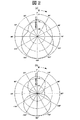
図2は、本実施の形態のループアンテナの一例の指向特性を示すグラフである。
この図2に示すグラフは、ループ形導体1の一辺の長さ(2S)を0.3lλo(2S=0.3lλo)とし、ループ形導体1と給電導体(21,22)とが形成される面と、導波板4との間隔(h)を0.0635λo(h=0.0635λo)とし、導波板4の一辺の長さ(L)を0.35λo(L=0.35λo)とした時の指向性を示すグラフである。
図2(a)は、図1に示すX−Z面(磁界面)の指向性を、図2(b)は、図1に示すY−Z面(電界面)の指向性を示している。
こられのグラフから分かるように、いずれの面の指向性も、−Z方向に最大放射方向となりながら、ほぼ同等のビ−ム幅で、F/B比は、従来のアンテナ同様に、ほぼ−10dB(放射方向が180°方向異なるために、符合が反転している)程度になっている。
【0014】
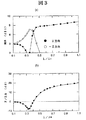
図3は、本実施の形態のループアンテナにおいて、正方形からなる導波板4の一辺の長さ(L)を変化させたときの、図1に示すZ方向、並びに−Z方向の利得と、F/Bの値の変化を示すグラフである。
図3(A)に示すグラフは、本実施の形態のループアンテナにおいて、ループ形導体1の一辺の長さ(2S)を0.31λo(2S=0.31λo)とし、ループ形導体1と給電導体(21,22)とが形成される面と、導波板4との間隔(h)を0.0635λo(h=0.0635λo)とし、正方形からなる導波板4の一辺の長さ(L)を変化させたときの、図1に示すZ方向、並びに−Z方向の利得の変化を示すグラフである。
図3(b)は、前記と同じ条件の下で、正方形からなる導波板4の一辺の長さ(L)を変化させたときの、F/Bの値の変化を示すグラフである。
【0015】
図3に示すグラフから分かるように、導波板4の一辺の長さ(L)が、0.2λo〜0.4λoの範囲において、−Z方向の放射(所謂、バックファイヤー)を生じている。
導波板4の一辺の長さ(L)が、0.2λo〜0.4λoの範囲内において、最大の利得が得られる導波板4の一辺の長さ(L)は、0.35λo付近で、利得は7.7dBiと最大となっているが、F/Bの極小値はこの0.35λoより僅かに小さい部分に存在しているため、用途に合わせて、導波板4の一辺の長さ(L)を選ぶ必要がある。
なお、本実施の形態のループアンテナでは、指向特性は、前述の通り導波板4の一辺の長さ(L)の他、導波板4とループ形導体1との間隔(h)によっても多少変化する。
また、入力インピーダンスは、ループ形導体1の大きさや、ループ形導体1、給電導体(21,22)、平衡線路(31,32)の太さ、導波板4とループ形導体1との間隔(h)、さらには平衡線路(31,32)の間隔によっても変化するので、使用する周波数帯に合わせて、相互の寸法を調整し、指向性を見ながら導波板4の一辺の長さ(L)を微調させて各部の寸法を決定する必要がある。
【0016】
なお、前述の説明では、導波板4の形状が正方形の場合を例に挙げて説明したが、導波板4の寸法は、ループ形導体1の電界方向(図1では、Y軸方向)に依存するため、矩形を選んだ場合には、電界方向の長さを0.2λo〜0.4λoに選ぶことにより、−Z方向の放射(所謂、バックファイヤー)を生ずる。
さらに、導波板4の形状を円形とした場合には、周囲長が正方形のそれと同じようにすることで、等価な特性となるため、その直径を0.25λo〜0.5λoに選ぶことにより、−Z方向の放射(所謂、バックファイヤー)を生ずる。
このように、正方形以外の形状であっても、ループ形導体1の電界方向と一致する方向の導波板4の大きさを決定することで、−Z方向の放射(所謂、バックファイヤー)を生ずることは言うまでも無い。
【0017】
また、前述の説明では、ループ形導体1が正方形の場合を例に挙げて説明したが、給電導体(21,22)の平衡線路側の端子(給電点)から見た各々のループの長さが約1λoに選ばれていれば、円形でも矩形でも楕円形でも構わず、さらに、図1に示すように、2つのループを組み合わせたものに限らず、一つのループの長さが、給電導体(21,22)の平衡線路側の端子(給電点)から見て約1λoに選ばれているものでも、0.5dB程度利得が減少するが、同様な効果を得ることができる。
本実施の形態のループアンテナを、軸対称形パラボラアンテナの放射素子に使用する場合には、従来の反射板付きループアンテナのように、パラボラアンテナの放射方向に位置する反射板14の背面より、反射板付きループアンテナに給電する必要がないので、パラボラアンテナの放射方向から給電する場合のような損失がなく、かつ、導波板4を正方形とした場合には、その一辺の長さ(L)が0.2λo〜0.4λoの長さであるため、パラボラアンテナのブロッキング面積を増大させることもなく、効率低下を招くこともなくなる。
【0018】
[実施の形態2]
図4は、本発明の実施の形態2のループアンテナの概略構成を示す斜視図である。
本実施の形態のループアンテナは、前記実施の形態のループアンテナを偏波共用のアンテナとした実施の形態である。
そのため、本実施の形態では、図4に示すように、図1に示すY軸方向に、第2の給電導体(201、202)、第2の平衡線路(301、302)が設けられる。
この第2の給電導体(201,202)は、一端が、ループ形導体1のある一辺(図1に示すY軸方向の辺の一つ)の中央に接続され、他端が、第2の平衡線路(301,302)の端部に接続されている。
ここで、給電導体201の平衡線路側の端子(給電点)から時計回り、および反時計回りに、給電導体202の平衡線路側の端子(給電点)までの長さは、約1λo(λoは、設計中心周波数の自由空間波長)に選ばれている。
第2の給電導体(201,202)、および第2の平衡線路(301,302)は、前記実施の形態と同様、金属などの導電体の板、管、線、条などで形成される。
なお、ループ形導体1、第1の給電導体(21,22)および第2の給電導体(201,202)は、誘電体面上に蒸着または圧着せしめた金属薄膜をエッチング手法等によって不必要な部分を取り除いて形成しても良い。
【0019】
さらに、本実施の形態では、第2の同軸線路50と、第2の同軸接栓60とが設けられ、第2の同軸線路50は、その端部において、外導体が導波板4に接続され、芯導体が導波板4に設けられた穴を貫通して平衡導体301に接続される。
同軸接栓60を介して入力された高周波電力は、同軸線路50、平衡導体301に接続され、給電導体201を介して、ループ形導体1を励振させる。
これにより、本実施の形態では、直交する偏波間の結合を−20dB以下と良好な状態に保ちつつ、互いの端子に対応する指向性や利得値は、図2に示すグラフと等価である。
但し、偏波が直交しているために、X−Y面の結果と、Y−Z面の測定結果とを入れ替えなければならないことは言うまでもない。
【0020】
本実施の形態のループアンテナでも、指向特性は、前述の通り導波板4の一辺の長さ(L)の他、導波板4とループ形導体1との間隔によっても多少変化する。
また、入力インピーダンスは、ループ形導体1の大きさや、ループ形導体1、給電導体(21,22,201,202)、平衡線路(31,32,301,302)の太さ、導波板4とループ形導体1との間隔(h)、さらには平衡線路(31,32,301,302)の間隔によっても変化するので、使用する周波数帯に合わせて、相互の寸法を調整し、指向性を見ながら導波板4の一辺の長さ(L)を微調させて各部の寸法を決定する必要がある。
また、前述したように、導波板4の寸法は、ループ形導体1の電界方向(図1では、X、Y軸方向)に依存するため、矩形を選んだ場合には、電界方向の長さを0.2λo〜0.4λoに選ぶことにより、−Z方向の放射(所謂、バックファイヤー)が生ずる。
さらに、前述したように、導波板4の形状を円形とした場合には、直径を0.25λo〜0.5λoに選ぶことにより、−Z方向の放射(所謂、バックファイヤー)が生ずる。
【0021】
このように、正方形以外の形状であっても、ループ形導体1の電界方向と一致する方向の導波板4の大きさを決定することによって、Z方向の放射(所謂、バックファイヤー)を生ずることは言うまでもない。
さらに、本実施の形態においても、ループ形導体1は、給電導体(21,22,201,202)の平衡線路側の端子(給電点)から見た各々のループの長さが約1λoに選ばれていれば、矩形でも楕円形でも構わない。
さらに、図4に示すように、2つのループを組み合わせたものに限らず、一つのループの長さが、給電導体(21,22,201,202)の平衡線路側の端子(給電点)から見て約1λoに選ばれているものでも、多少利得が減少するが、同様な効果を得ることができる。
本実施の形態のループアンテナを、軸対称形パラボラアンテナの放射素子に使用する場合には、従来の反射板付きループアンテナのように、パラボラアンテナの放射方向から給電する場合のような損失がなく、かつ、導波板4を正方形とした場合には、その一辺の長さ(L)が0.2λo〜0.4λoの長さであるため、パラボラアンテナのブロッキング面積を増大させることもなく、効率低下を招くこともなくなる。
【0022】
[実施の形態3]
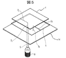
図5は、本発明の実施の形態3のループアンテナの概略構成を示す斜視図である。
本実施の形態のループアンテナは、図6に示す反射板14の前面に、導波板4を配置した実施の形態である。
本実施の形態でも、ループ形導体1、給電導体(21,22)、および平衡線路(31,32)は、金属などの導電体の板、管、線、条などで形成される。
なお、ループ形導体1と給電導体(21,22)とは、誘電体面上に蒸着または圧着せしめた金属薄膜をエッチング手法等によって不必要な部分を取り除いて形成しても良い。
また、本実施の形態では、同軸線路5は、その端部において、外導体が反射板14に接続され、芯導体が反射板14に設けられた穴を貫通して平衡導体31に接続される。
【0023】
本実施の形態のループアンテナでは、導波板4により、図1に示すZ方向に放射される電界と、反射板14によって反射される電界とが合成されることで、利得が増大される他、F/B比を改善させ、通信における目的方向以外に対する干渉を低減させることができる。
また、容易にエンドファイヤー形式で、偏波共用させた高利得アンテナを実現することができる。
通常、周波数が高くなると、工作精度を高めないと所望の特性を維持することが難しくなるが、本実施の形態によれば、導波板4の精度だけに依存されるために、エンドファイヤーアンテナとして、従来使用されているループ導体を並べたループ八木アンテナに比べて製作が容易で支持しやすい。
なお、図5では、導波板4が一枚の場合を示しているが、複数の導波板4を配置して周期構造させ、要求される利得の値やビーム幅にさせることができることはいうまでもない。
また、ループ形導体1および導波板4の形状は、いかなる形状であっても実現可能であり、その組み合わせに関しても、柔軟であることは前述の通りである。以上、本発明者によってなされた発明を、前記実施の形態に基づき具体的に説明したが、本発明は、前記実施の形態に限定されるものではなく、その要旨を逸脱しない範囲において種々変更可能であることは勿論である。
【0024】
【発明の効果】
本願において開示される発明のうち代表的なものによって得られる効果を簡単に説明すれば、下記の通りである。
(1)本発明によれば、ループ形放射素子上に導波板を配置し、導波板が配置される方向に最大放射方向の指向特性を持つループアンテナを提供することができる。
(2)本発明によれば、小型で単一指向性を得ることを目的としたバックファイヤー形の放射素子や、高利得特性が要求されるエンドファイヤー形アンテナに最適なループアンテナを提供することができる。
【図面の簡単な説明】
【図1】本発明の実施の形態1のループアンテナの概略構成を示す斜視図である。
【図2】本発明の実施の形態1のループアンテナの一例の指向特性を示すグラフである。
【図3】本実施の形態のループアンテナにおいて、正方形からなる導波板の一辺の長さ(L)を変化させたときの、図1に示すZ方向、並びに−Z方向の利得と、F/Bの値の変化を示すグラフである。
【図4】本発明の実施の形態2のアンテナの概略構成を示す斜視図である。
【図5】本発明の実施の形態3のアンテナの概略構成を示す斜視図である。
【図6】従来の反射板付きループアンテナの概略構成を示す斜視図である。
【図7】図6に示す反射板付きループアンテナの一例の指向特性を示すグラフである。
【符号の説明】
1,11…ループ形導体、21,22,121,122,201,202…給電導体、31、32,131,132,301,302…平衡線路、4…導波板、5,15,50…同軸線路、6,16,60…同軸接栓、14…反射板。[0001]
BACKGROUND OF THE INVENTION
The present invention relates to a loop antenna, and in particular, a backfire type radiating element aiming at obtaining a small directivity, such as a primary radiator of a parabolic antenna, and a high gain characteristic are required. The present invention relates to a loop antenna optimal for an endfire type antenna.
[0002]
[Prior art]
FIG. 6 is a perspective view showing a schematic configuration of a conventional loop antenna with a reflector.
In the figure,
The loop-
The loop-
[0003]
The distance (h) between the
The high frequency power input through the
[0004]
FIG. 7 is a graph showing directivity characteristics of an example of the loop antenna with a reflector shown in FIG.
In the graph shown in FIG. 7, the length (2S) of one side of the loop-
7A shows the directivity of the XZ plane (magnetic field plane) shown in FIG. 6, and FIG. 7B shows the directivity of the YZ plane (electric field plane) shown in FIG.
As can be seen from FIG. 7, the directivity of any surface has almost the same beam width, and the directivity ratio (F / B ratio) of the front to back is about 10 dB.
[0005]
[Problems to be solved by the invention]
In the case of a conventional loop antenna with a reflector, radio waves are radiated in the Z-axis direction of the coordinate system shown in FIG.
Therefore, when the loop antenna with a reflector shown in FIG. 6 is used as a radiating element of an axisymmetric parabolic antenna, power is supplied to the loop antenna with a reflector from the back of the
Therefore, the loss when power is fed from the radiation direction of the parabolic antenna is not negligible, and when the
The present invention has been made to solve the problems of the prior art, and the object of the present invention is to arrange a waveguide plate on a loop-type radiating element and to maximize the direction in which the waveguide plate is arranged. An object of the present invention is to provide a loop antenna having a radiation direction characteristic.
The above and other objects and novel features of the present invention will become apparent from the description of this specification and the accompanying drawings.
[0006]
[Means for Solving the Problems]
Of the inventions disclosed in this application, the outline of typical ones will be briefly described as follows.
That is, the present invention includes a loop-shaped radiating element formed of a conductive plate, a loop antenna and a waveguide plate which is arranged at a predetermined distance with respect to said loop-shaped radiating element, said loop-shaped the radiating element, through the waveguide plate, the said loop-shaped radiating element of the wave guide is powered from the opposite side, the directional characteristics with maximum radiation in the direction toward the waveguide plate from said loop-shaped radiating element It is characterized by having .
[0007]
Also, in a preferred embodiment of the present invention, the waveguide plate is formed of a rectangular conductive plate, and when the free space wavelength of the design center frequency of the loop radiating element is λo, the rectangular shape The conductive plate is characterized in that the length in the electric field direction is shorter than 0.4λo.
In a preferred embodiment of the present invention, the waveguide plate is formed of a circular conductive plate, and the circular conductive plate has a free space wavelength of λo at a design center frequency of the loop-type radiating element. The plate is characterized in that the diameter is shorter than 0.5λo.
Furthermore, in a preferred embodiment of the present invention, the loop-type radiating element is a dual-polarized radiating element that radiates and receives two radio waves having different polarization directions.
[0008]
In a more preferred embodiment of the present invention, the loop-type radiating element includes a closed-loop loop element, and first and second feeding conductors each having one terminal connected to the closed-loop loop element. When the free space wavelength of the design center frequency of the loop-type radiating element is λo, the second feeding conductor is rotated clockwise and counterclockwise from the other terminal of the first feeding conductor. The length to the other terminal is about λo.
In a more preferred embodiment of the present invention, the loop-type radiating element is connected between a first feeding conductor, a second feeding conductor, and one terminal of the first and second feeding conductors. Loop element, and the free space wavelength of the design center frequency of the loop-type radiating element is λo, the length from the other terminal of the first power supply conductor to the other terminal of the second power supply conductor Is about λo.
[0009]
In a more preferred embodiment of the present invention, the loop radiating element includes a closed loop loop element, and first to fourth feed conductors each having one terminal connected to the closed loop loop element. And when the free space wavelength of the design center frequency of the loop-type radiating element is λo, the first power supply conductor and the first power supply conductor are rotated clockwise and counterclockwise from the other terminal of the first power supply conductor. The length to the other terminal of the second power supply conductor forming a pair and the third power supply conductor are paired clockwise and counterclockwise from the other terminal of the third power supply conductor. The length to the other terminal of the fourth feeding conductor is about λo.
[0010]
In a more preferred embodiment of the present invention, the loop-type radiating element is connected between a first feeding conductor, a fourth feeding conductor, and one terminal of the first and fourth feeding conductors. A loop element, one terminal connected to the loop element, a second power supply conductor paired with the first power supply conductor, and one terminal connected to the loop element, the fourth power supply conductor And a loop element connected between one terminal of the first and fourth power supply conductors, and the free space wavelength of the design center frequency of the loop-type radiating element is λo The length from the other terminal of the first power supply conductor to the other terminal of the second power supply conductor, and the other terminal of the fourth power supply conductor from the other terminal of the third power supply conductor. The length to the terminal is about λo.
[0011]
DETAILED DESCRIPTION OF THE INVENTION
Hereinafter, embodiments of the present invention will be described in detail with reference to the drawings.
Note that components having the same function are denoted by the same reference symbols throughout the drawings for describing the embodiment, and the repetitive description thereof will be omitted.
[Embodiment 1]
FIG. 1 is a perspective view showing a schematic configuration of a loop antenna according to Embodiment 1 of the present invention.
In the figure, reference numeral 1 denotes a loop-shaped conductor (loop-shaped radiating element of the present invention). In FIG. 1, the shape of the loop-shaped conductor 1 is a square.
2 1 , 2 2 are feed conductors, 3 1 , 3 2 are balanced lines, and the feed conductors (2 1 , 2 2 ) have one end on one side of the loop-shaped conductor 1 (in the X-axis direction shown in FIG. 1). Is connected to the center of one of the sides) and the other end is connected to the end of the balanced line (3 1 , 3 2 ).
Here, clockwise from the
[0012]
The loop-shaped conductor 1, the feeding conductors (2 1 , 2 2 ), and the balanced lines (3 1 , 3 2 ) are formed of a conductive plate such as metal, a tube, a wire, a strip, or the like.
The loop-shaped conductor 1 and the power supply conductors (2 1 , 2 2 ) may be formed by removing unnecessary portions of the metal thin film deposited or pressure-bonded on the dielectric surface by an etching method or the like.
The high-frequency power input through the
[0013]
FIG. 2 is a graph showing the directivity characteristics of an example of the loop antenna according to the present embodiment.
In the graph shown in FIG. 2, the length (2S) of one side of the loop-shaped conductor 1 is 0.3lλo (2S = 0.3lλo), and the loop-shaped conductor 1 and the feed conductors (2 1 , 2 2 ) are formed. The distance (h) between the surface to be guided and the
2A shows the directivity of the XZ plane (magnetic field plane) shown in FIG. 1, and FIG. 2B shows the directivity of the YZ plane (electric field plane) shown in FIG. .
As can be seen from these graphs, the directivity of any surface is the same as the maximum radiation direction in the -Z direction, and the beam width is almost the same, and the F / B ratio is substantially -as in the conventional antenna. It is about 10 dB (the sign is reversed because the radiation direction is different by 180 °).
[0014]
3 shows gains in the Z direction and the −Z direction shown in FIG. 1 when the length (L) of one side of the
The graph shown in FIG. 3A shows that in the loop antenna according to the present embodiment, the length (2S) of one side of the loop conductor 1 is 0.31λo (2S = 0.31λo), and the loop conductor 1 and the power supply are fed. The distance (h) between the surface on which the conductor (2 1 , 2 2 ) is formed and the
FIG. 3B is a graph showing the change in the value of F / B when the length (L) of one side of the
[0015]
As can be seen from the graph shown in FIG. 3, radiation in the -Z direction (so-called backfire) occurs when the length (L) of one side of the
When the length (L) of one side of the
In the loop antenna according to the present embodiment, the directivity is determined not only by the length (L) of one side of the
Also, the input impedance is the size of the loop conductor 1, the loop conductor 1, the feed conductors (2 1 , 2 2 ), the thickness of the balanced lines (3 1 , 3 2 ), the
[0016]
In the above description, the case where the shape of the
Furthermore, when the shape of the
In this way, even in a shape other than a square, by determining the size of the
[0017]
In the above description, the case where the loop-shaped conductor 1 is a square is described as an example. However, each loop viewed from the terminal (feeding point) on the balanced line side of the feeding conductor (2 1 , 2 2 ) is described. If the length is selected to be about 1λo, it may be circular, rectangular, or elliptical, and as shown in FIG. 1, the length of one loop is not limited to a combination of two loops. Even when the power supply conductor (2 1 , 2 2 ) is selected at about 1λo when viewed from the balanced line side terminal (feed point), the gain is reduced by about 0.5 dB, but the same effect can be obtained. .
When the loop antenna according to the present embodiment is used for a radiating element of an axisymmetric parabolic antenna, like a conventional loop antenna with a reflecting plate, from the back surface of the reflecting
[0018]
[Embodiment 2]
FIG. 4 is a perspective view showing a schematic configuration of the loop antenna according to the second embodiment of the present invention.
The loop antenna of the present embodiment is an embodiment in which the loop antenna of the above-described embodiment is a polarization sharing antenna.
Therefore, in the present embodiment, as shown in FIG. 4, the second power supply conductors (20 1 , 20 2 ) and the second balanced lines (30 1 , 30 2 ) are arranged in the Y-axis direction shown in FIG. Provided.
One end of the second feeding conductor (20 1 , 20 2 ) is connected to the center of one side of the loop-shaped conductor 1 (one of the sides in the Y-axis direction shown in FIG. 1), and the other end is Two balanced lines (30 1 , 30 2 ) are connected to the ends.
Here, clockwise from the feeding
The second feeder conductor (20 1 , 20 2 ) and the second balanced line (30 1 , 30 2 ) are made of a conductive plate such as metal, a tube, a wire, a strip, etc., as in the above embodiment. It is formed.
The loop-shaped conductor 1, the first power supply conductor (2 1 , 2 2 ) and the second power supply conductor (20 1 , 20 2 ) are formed by etching a metal thin film deposited or pressure-bonded on the dielectric surface. It may be formed by removing unnecessary portions.
[0019]
Further, in the present embodiment, a second
The high frequency power input through the
Thereby, in this Embodiment, the directivity and gain value corresponding to each other terminal are equivalent to the graph shown in FIG. 2 while maintaining the coupling between orthogonal polarizations in a favorable state of −20 dB or less.
However, since the polarization is orthogonal, it goes without saying that the result on the XY plane and the measurement result on the YZ plane must be interchanged.
[0020]
Also in the loop antenna of the present embodiment, the directivity changes somewhat depending on the distance between the
The input impedance is determined by the size of the loop conductor 1, the loop conductor 1, the feed conductor (2 1 , 2 2 , 20 1 , 20 2 ), the balanced line (3 1 , 3 2 , 30 1 , 30 2 ). The frequency varies depending on the thickness, the distance (h) between the
Further, as described above, the dimension of the
Further, as described above, when the shape of the
[0021]
In this way, even if the shape is other than a square, by determining the size of the
Further, also in the present embodiment, the loop conductor 1 has the length of each loop as viewed from the balanced line side terminals (feed points) of the feed conductors (2 1 , 2 2 , 20 1 , 20 2 ). If it is selected to be about 1λo, it may be rectangular or elliptical.
Further, as shown in FIG. 4, the length of one loop is not limited to a combination of two loops, and the terminal on the balanced line side of the feed conductor (2 1 , 2 2 , 20 1 , 20 2 ) ( Even if the gain is selected to be about 1λo as viewed from the feeding point), the gain is somewhat reduced, but the same effect can be obtained.
When the loop antenna of this embodiment is used as a radiation element of an axisymmetric parabolic antenna, there is no loss as in the case of feeding from the radiation direction of the parabolic antenna, unlike the conventional loop antenna with a reflector. And when the
[0022]
[Embodiment 3]
FIG. 5 is a perspective view showing a schematic configuration of the loop antenna according to the third embodiment of the present invention.
The loop antenna according to the present embodiment is an embodiment in which the
Also in the present embodiment, the loop-shaped conductor 1, the feed conductors (2 1 , 2 2 ), and the balanced lines (3 1 , 3 2 ) are formed of a conductive plate such as metal, a tube, a wire, a strip, or the like. The
The loop-shaped conductor 1 and the power supply conductors (2 1 , 2 2 ) may be formed by removing unnecessary portions of the metal thin film deposited or pressure-bonded on the dielectric surface by an etching method or the like.
Further, in this embodiment, the
[0023]
In the loop antenna of this embodiment, the
In addition, it is possible to easily realize a high gain antenna in which the polarization is shared in the endfire format.
Normally, when the frequency is increased, it is difficult to maintain desired characteristics unless the working accuracy is increased. However, according to the present embodiment, since it depends only on the accuracy of the
FIG. 5 shows a case where the number of the
The loop conductor 1 and the
[0024]
【The invention's effect】
The effects obtained by the representative ones of the inventions disclosed in the present application will be briefly described as follows.
(1) According to the present invention, it is possible to provide a loop antenna in which a waveguide plate is arranged on a loop-type radiating element and the directivity characteristic of the maximum radiation direction is provided in the direction in which the waveguide plate is arranged.
(2) According to the present invention, there is provided a loop antenna that is optimal for a backfire-type radiating element that is small in size and has a single directivity and an endfire-type antenna that requires high gain characteristics. Can do.
[Brief description of the drawings]
FIG. 1 is a perspective view showing a schematic configuration of a loop antenna according to a first embodiment of the present invention.
FIG. 2 is a graph showing directivity characteristics of an example of a loop antenna according to the first embodiment of the present invention.
3 shows gains in the Z direction and −Z direction shown in FIG. 1 when the length (L) of one side of a square waveguide plate is changed in the loop antenna of the present embodiment, and F It is a graph which shows the change of the value of / B.
FIG. 4 is a perspective view showing a schematic configuration of an antenna according to a second embodiment of the present invention.
FIG. 5 is a perspective view showing a schematic configuration of an antenna according to a third embodiment of the present invention.
FIG. 6 is a perspective view showing a schematic configuration of a conventional loop antenna with a reflector.
7 is a graph showing directivity characteristics of an example of the loop antenna with a reflector shown in FIG. 6;
[Explanation of symbols]
1, 11... Loop-shaped conductor, 2 1 , 2 2 , 12 1 , 12 2 , 20 1 , 20 2 ... Feeding conductor, 3 1 , 3 2 , 13 1 , 13 2 , 30 1 , 30 2 . 4 ... Waveguide plate, 5, 15, 50 ... Coaxial line, 6, 16, 60 ... Coaxial plug, 14 ... Reflector.
Claims (4)
導電板で構成され、前記ループ形放射素子に対して所定の間隔をおいて配置される導波板とを有し、
前記ループ形放射素子には、前記導波板を通して、前記導波板の前記ループ形放射素子と反対側から給電され、
前記ループ形放射素子から前記導波板に向かう方向に最大放射方向を持つ指向特性を有することを特徴とするループアンテナ。A loop radiating element;
A conductive plate, and a waveguide plate disposed at a predetermined interval with respect to the loop radiating element,
The loop-shaped radiating element is fed through the waveguide plate from the side opposite to the loop-shaped radiating element of the waveguide plate,
A loop antenna having a directivity characteristic having a maximum radiation direction in a direction from the loop radiation element toward the waveguide plate.
前記ループ形放射素子の設計中心周波数の自由空間波長をλoとするとき、前記導波板は、電界方向の長さが、0.4λoより短いことを特徴とする請求項1に記載のループアンテナ。 The waveguide plate is composed of a rectangular conductive plate,
2. The loop antenna according to claim 1 , wherein when the free space wavelength of the design center frequency of the loop radiating element is λo, the length of the waveguide plate in the electric field direction is shorter than 0.4λo. .
前記ループ形放射素子の設計中心周波数の自由空間波長をλoとするとき、前記導波板は、直径が、0.5λoより短いことを特徴とする請求項1に記載のループアンテナ。 The waveguide plate is composed of a circular conductive plate,
2. The loop antenna according to claim 1 , wherein the waveguide plate has a diameter shorter than 0.5λo when a free space wavelength of a design center frequency of the loop-shaped radiating element is λo.
Priority Applications (1)
| Application Number | Priority Date | Filing Date | Title |
|---|---|---|---|
| JP2000045395A JP4108246B2 (en) | 2000-02-23 | 2000-02-23 | Loop antenna |
Applications Claiming Priority (1)
| Application Number | Priority Date | Filing Date | Title |
|---|---|---|---|
| JP2000045395A JP4108246B2 (en) | 2000-02-23 | 2000-02-23 | Loop antenna |
Publications (2)
| Publication Number | Publication Date |
|---|---|
| JP2001237637A JP2001237637A (en) | 2001-08-31 |
| JP4108246B2 true JP4108246B2 (en) | 2008-06-25 |
Family
ID=18567988
Family Applications (1)
| Application Number | Title | Priority Date | Filing Date |
|---|---|---|---|
| JP2000045395A Expired - Fee Related JP4108246B2 (en) | 2000-02-23 | 2000-02-23 | Loop antenna |
Country Status (1)
| Country | Link |
|---|---|
| JP (1) | JP4108246B2 (en) |
Families Citing this family (4)
| Publication number | Priority date | Publication date | Assignee | Title |
|---|---|---|---|---|
| JP3791923B2 (en) | 2004-01-13 | 2006-06-28 | 株式会社東芝 | Wireless communication terminal |
| JP4511382B2 (en) * | 2005-02-21 | 2010-07-28 | 古野電気株式会社 | Circularly polarized loop antenna |
| JP5699305B2 (en) * | 2011-05-13 | 2015-04-08 | 株式会社国際電気通信基礎技術研究所 | antenna |
| JP7091952B2 (en) * | 2018-08-31 | 2022-06-28 | 株式会社村田製作所 | Directional antenna |
-
2000
- 2000-02-23 JP JP2000045395A patent/JP4108246B2/en not_active Expired - Fee Related
Also Published As
| Publication number | Publication date |
|---|---|
| JP2001237637A (en) | 2001-08-31 |
Similar Documents
| Publication | Publication Date | Title |
|---|---|---|
| US8766866B2 (en) | Log periodic antenna | |
| KR20060066717A (en) | Broadband multi-dipole antenna with frequency-independent radiation characteristics | |
| JP2009089212A (en) | Antenna for radar device | |
| JPH10150319A (en) | Dipole antenna with reflecting plate | |
| JPH04369905A (en) | Circularly polarized dielectric antenna | |
| US9263807B2 (en) | Waveguide or slot radiator for wide E-plane radiation pattern beamwidth with additional structures for dual polarized operation and beamwidth control | |
| US20230075273A1 (en) | Magneto-electric dipole antenna | |
| JP3176217B2 (en) | Antenna device | |
| JP3026171B2 (en) | Antenna device | |
| JP4516246B2 (en) | antenna | |
| CN115775971A (en) | Dual-frequency broadband high-gain printed omnidirectional antenna based on multimode resonance | |
| JP2000196344A (en) | Antenna device | |
| JP3804878B2 (en) | Dual-polarized antenna | |
| JP4108246B2 (en) | Loop antenna | |
| CN115117611B (en) | Sidelobe-controllable high-gain high-order mode compressed dipole antenna loaded with bending lines and design method thereof | |
| CN110635230A (en) | Asymmetric dual-polarized antenna device based on SICL resonant cavity circular ring gap and printed oscillator | |
| JP3058874B1 (en) | Waveguide-fed array antenna | |
| JP2001345630A (en) | Slot antenna | |
| JP3038205B1 (en) | Waveguide-fed planar antenna | |
| CN220492202U (en) | Broadband end-fire antenna applied to X frequency band | |
| JPH0324805A (en) | Slot type stacked spiral antenna | |
| JP3716991B2 (en) | Dual frequency antenna | |
| JP2006014152A (en) | Plane antenna | |
| JP3364204B2 (en) | Antenna device | |
| JP3360118B2 (en) | Horizontally polarized antenna |
Legal Events
| Date | Code | Title | Description |
|---|---|---|---|
| A621 | Written request for application examination |
Free format text: JAPANESE INTERMEDIATE CODE: A621 Effective date: 20060823 |
|
| A977 | Report on retrieval |
Free format text: JAPANESE INTERMEDIATE CODE: A971007 Effective date: 20080111 |
|
| A131 | Notification of reasons for refusal |
Free format text: JAPANESE INTERMEDIATE CODE: A131 Effective date: 20080122 |
|
| A521 | Written amendment |
Free format text: JAPANESE INTERMEDIATE CODE: A523 Effective date: 20080314 |
|
| TRDD | Decision of grant or rejection written | ||
| A01 | Written decision to grant a patent or to grant a registration (utility model) |
Free format text: JAPANESE INTERMEDIATE CODE: A01 Effective date: 20080401 |
|
| A61 | First payment of annual fees (during grant procedure) |
Free format text: JAPANESE INTERMEDIATE CODE: A61 Effective date: 20080402 |
|
| FPAY | Renewal fee payment (event date is renewal date of database) |
Free format text: PAYMENT UNTIL: 20110411 Year of fee payment: 3 |
|
| R150 | Certificate of patent or registration of utility model |
Free format text: JAPANESE INTERMEDIATE CODE: R150 |
|
| FPAY | Renewal fee payment (event date is renewal date of database) |
Free format text: PAYMENT UNTIL: 20110411 Year of fee payment: 3 |
|
| R250 | Receipt of annual fees |
Free format text: JAPANESE INTERMEDIATE CODE: R250 |
|
| R250 | Receipt of annual fees |
Free format text: JAPANESE INTERMEDIATE CODE: R250 |
|
| LAPS | Cancellation because of no payment of annual fees |