JP4105281B2 - Optical head and manufacturing method thereof - Google Patents
Optical head and manufacturing method thereof Download PDFInfo
- Publication number
- JP4105281B2 JP4105281B2 JP09796398A JP9796398A JP4105281B2 JP 4105281 B2 JP4105281 B2 JP 4105281B2 JP 09796398 A JP09796398 A JP 09796398A JP 9796398 A JP9796398 A JP 9796398A JP 4105281 B2 JP4105281 B2 JP 4105281B2
- Authority
- JP
- Japan
- Prior art keywords
- light
- optical
- filter
- optical head
- film
- Prior art date
- Legal status (The legal status is an assumption and is not a legal conclusion. Google has not performed a legal analysis and makes no representation as to the accuracy of the status listed.)
- Expired - Fee Related
Links
Images


Description
【0001】
【発明の属する技術分野】
本発明は、レーザ光を利用してデータの再生や記録を行う光ディスク装置に用いられ得て、信号の読み取り及び/或いは記録を行う光ヘッド、並びにその製造方法に関する。
【0002】
【従来の技術】
近年、光ディスク媒体が大容量データファイルとして実用化されるに至っているが、更に様々な用途への適用を目指して、その更なる大容量化の実現が課題となっている。光ディスク装置の記録密度は、線密度方向については、パーシャルレスポンス技術により約0.3μm/bitの記録密度が実用化されてきており、一方、トラック方向については、約1.2μm/trackの記録密度が実用化されてきている。
【0003】
光ディスク装置の記録密度の向上は、光ヘッドによって集光される光ビームが光ディスク媒体の上に形成する光スポットのサイズの減少によって、実現され得る。光ヘッドにより形成されるこのような光スポットのサイズは、一般に、使用される光源の波長及び集光レンズの開口で決まる。そこで、これらのパラメータの改良によって光スポットのサイズを減少し、それによって光ディスク装置の記録密度を向上させようとする様々なシステムが、提案されている。
【0004】
その一つは、例えば特開平5−135401号公報や米国特許第5,590,110号に開示されているような、光ディスク媒体からの反射光をレンズを使ってもう一度集束させ、この集束された光ビームの中心部の光だけをピンホールフィルタのピンホール領域を透過させることによって分離して検出するシステム(方式)である。このようなシステムでは、光源の波長及び集光レンズの開口で決まる本来の分解能の値に比べて、さらに高い分解能で信号を再生することが可能となり、高密度の光ディスク装置が実現できる。以下では、この方式を「光ヘッド超解像再生方式」と呼ぶ。
【0005】
【発明が解決しようとする課題】
従来技術による光ヘッド超解像再生方式では、集束された光ビームの中心部に、ピンホールフィルタのピンホール領域をミクロンオーダの高精度で位置決めする必要がある。この場合、レンズからの焦点距離方向での位置決めは、設計に基づく所定の位置にピンホールフィルタを配置することで、ある程度まで容易に実現され得る。しかし、光ヘッド超解像再生方式を十分に機能させるためには、集束された光ビームがピンホールフィルタの微少なピンホール領域を正確に通過することが必要であり、そのためには、レンズから焦点距離だけ離れた位置における光軸に垂直な平面(以下では、「焦点距離面」とも称する)の面内で、ピンホールフィルタを2次元的に正確に位置決めしなければならない。
【0006】
しかし、実際には、このようなピンホール領域の位置決め作業(特に、上記の焦点距離面内での2次元的な位置決め作業)の精度を十分に確保することができず、結果として、光ヘッド超解像再生方式の実用化が非常に困難となっている。
【0007】
本発明は、上記の課題を考慮してなされたものであり、その目的は、(1)集束された光ビームの中心部分の光のみを通過させるフィルタ(ピンホールフィルタ)を容易に且つ高精度に形成・位置決めして、光ヘッド超解像再生方式による高密度の光ディスクの再生を可能にする光ヘッドの製造方法を提供すること、並びに(2)上記によって形成される光ヘッドを提供すること、である。
【0008】
【課題を解決するための手段】
本発明の光ヘッドは、光源と、受光する光に基づいて所定の信号を生成する光検出器と、前記光源から出射された光ビームを集光して所定の反射部材に照射する集光光学系と、前記所定の反射部材からの反射光を前記光検出器に導く再生光学系と、を備え、前記再生光学系は、光を所定の集束点に集束させるように構成されており、前記集束点の近傍には、該集束された光の中心近傍の部分を選択的に透過させる光透過領域を有するフィルタが設けられていて、該フィルタの前記光透過領域は、前記再生光学系の少なくとも一部を通過して集束された光によって形成されたものであり、前記再生光学系が、前記反射光を集束させる集束レンズを含んでおり、該集束レンズのレンズ形成面に対向する端面に、前記フィルタが設けられており、そのことによって、上記の目的が達成される。
【0009】
前記所定の反射部材は、光ディスク媒体であり得る。さらに、前記光ディスク媒体は、光磁気ディスク媒体であり得る。
【0011】
好ましくは、前記フィルタの前記光透過領域が、前記再生光学系を通過してきて集束された前記反射光によって形成される。
【0013】
他の実施形態では、前記集束レンズのレンズ形成面に対向する前記端面と前記フィルタとの間に、該集束レンズよりも高い屈折率を有する材料の膜が形成されている。
【0014】
ある実施形態では、前記フィルタは、融点が約500℃以下である材料の膜を利用して形成されている。例えば、前記材料の膜は、Te−C膜である。
【0015】
或いは、前記フィルタは、照射される光の光エネルギーによって透過率が可逆的に変化する色素の膜を利用して形成され得る。例えば、前記色素は、フォトクロミック系色素であり得る。
【0016】
ある実施形態では、前記フィルタの前記光透過領域は、前記再生光学系の光軸と該フィルタとが垂直な位置関係で配置されている場合の集束点からオフセットした位置に設けられている。
【0018】
本発明の光ヘッドの製造方法は、光源と、受光する光に基づいて所定の信号を生成する光検出器と、前記光源から出射された光ビームを集光して所定の反射部材に照射する集光光学系と、前記所定の反射部材からの反射光を前記光検出器に導く再生光学系と、を備える光ヘッドの製造方法であって、該方法は、前記再生光学系を、光を所定の集束点に集束させるように構成する工程と、該集束点の近傍に所定の材料の膜を設ける工程と、前記再生光学系の少なくとも一部を通過して集束された光を前記所定の材料の膜に照射して、該集束された光の中心近傍の部分を選択的に透過させる光透過領域を有するフィルタを形成する工程とを包含し、前記所定の材料の膜は、前記再生光学系に含まれていて前記反射光を集束させる集束レンズのレンズ形成面に対向する端面に設けられる。
【0020】
前記所定の反射部材は、光ディスク媒体であり得る。さらに、前記光ディスク媒体は、光磁気ディスク媒体であり得る。
【0023】
他の実施形態では、上記の製造方法は、前記集束レンズのレンズ形成面に対向する前記端面と前記所定の材料の膜との間に、該集束レンズよりも高い屈折率を有する材料の膜を形成する工程をさらに含む。
【0024】
ある実施形態では、前記所定の材料の膜は、融点が約500℃以下である材料の膜を利用して形成されている。例えば、前記材料の膜は、Te−C膜である。
【0025】
或いは、前記所定の材料の膜は、照射される光の光エネルギーによって透過率が可逆的に変化する色素の膜を利用して形成され得る。例えば、前記色素は、フォトクロミック系色素であり得る。
【0026】
ある実施形態では、前記フィルタの前記光透過領域は、前記再生光学系の光軸と該フィルタとが垂直な位置関係で配置されている場合の集束点からオフセットした位置に設けられる。
【0028】
ある実施形態では、前記フィルタの前記光透過領域を、前記反射部材で反射された後に前記再生光学系を通過してきて集束された前記反射光によって形成する。例えば、前記反射部材として光ディスク媒体を使用し、該光ディスク媒体で反射された後に前記再生光学系を通過してきて集束された前記反射光によって前記フィルタの前記光透過領域を形成してもよい。
【0029】
他の実施形態では、前記フィルタの形成工程が、前記所定の反射部材として反射板を置く工程と、該反射板で反射された後に前記再生光学系を通過してきて集束された前記反射光を前記所定の材料の膜に照射する工程と、を含む。
【0030】
【発明の実施の形態】
(第1の実施形態)
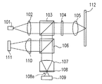
図1は、本発明の第1の実施形態における光ヘッドの構成を模式的に示す図である。
【0031】
図1の光学系において、光源である半導体レーザ101から発せられた出射光は、コリメートレンズ102によって平行光にされた後に、出射光と反射光とを分離する偏光ビームスプリッタ103、及び、偏光ビームスプリッタ103での出射光と反射光との分離を可能にするために光の偏光面を回転させる1/4波長板104を通過し、集光レンズ105によって光ディスク媒体112の面上に集光される。以上の構成を、本明細書では「集光光学系」とも称する。
【0032】
光ディスク媒体112からの反射光は、集光レンズ105で平行光にされた後に、1/4波長板104を通過し、偏光ビームスプリッタ103によって出射光の光路から分離されて、ハーフプリズム106に向かう。ハーフプリズム106では、反射光の一部が、フォーカストラッキング制御における誤差信号を検出するための光として分離される。分離された光は、検出レンズ110によって光検出器111に集光されて、そこでフォーカストラッキング制御のためのフォーカス誤差信号及びトラッキング誤差信号が検出される。一方、ハーフプリズム106を通過した残りの光は、集束レンズ107によって再び集束され、集束レンズ107と一体的に形成されているピンホールフィルタ108のピンホール領域(光透過領域)108aを通過して、光検出器109に入射する。光検出器109は、この入射光に基づいて、再生信号を生成する。以上のような偏光ビームスプリッタ103で分岐されてから光検出器111或いは109に至る構成を、本明細書では「再生光学系」とも称する。
【0033】
以上のような図1の光学系の構成におけるピンホールフィルタ108について、以下でさらに説明する。
【0034】
集束レンズ107は、その一方の面(入射面)にレンズ形状が形成されており、入射面に対向している他方の面(集光面)が、集束レンズ107(具体的には、入射面に形成されているレンズ形状)の焦点距離に相当する長さだけ入射面から離れているように、設計されている。この集光面に、スパッタリング法によってTi薄膜を厚さ約100nmに形成する。なお、以下の説明では、説明の簡略化のために、ピンホールフィルタに含まれるTi薄膜に、ピンホールフィルタと同じ参照番号「108」を付す)。
【0035】
次に、集束レンズ107の焦点位置に相当する箇所のTi薄膜108に、光学的なフィルタの役割を果たすピンホール領域108aを、例えば以下のようにして形成する。
【0036】
図2(a)は、ピンホール領域108aを形成するための光学系の配置を模式的に示す図である。具体的には、光源である半導体レーザ113から発せられた光を、コリメータレンズ114で平行光にした後に、半導体レーザ113からの出射光の光軸に垂直になるように位置調整されて配置されている集束レンズ107の入射面に入射させて、Ti薄膜108が形成されている集光面の上に焦点を結ばせる。これにより、集束レンズ107の焦点位置(集光部分)に相当する箇所のTi薄膜108の温度が上昇して融解し、ピンホール領域108aが形成される。これによって、光ビームの中心部分の光のみをピンホール領域108aを通って通過させるピンホールフィルタ108が、再生光学系(少なくとも、その一部である集束レンズ107)を実際に通過してきた光によって、集束レンズ107の集光面の上に形成される。
【0037】
このようにして集束レンズ107と一体的に形成されたピンホールフィルタ108を、図1の光学系における所定の位置に配置する。
【0038】
本実施形態の以上のような方法では、半導体レーザ113のレーザパワーを95mWに設定し、500nsのパルス光を照射することによって、良好なピンホール領域108aが形成される。
【0039】
図2(b)は、以上のようにして形成されるピンホールフィルタ108のピンホール領域(光透過領域)108aの近傍の断面形状を、拡大して模式的に示す図である。本実施形態によるピンホール領域108aは、Ti薄膜の熱的な融解によって形成されるので、ピンホール領域108aの周辺部が若干盛り上がった形状になっている。
【0040】
このようにして構成される本実施形態の光ヘッドの再生特性を、図3に示す。具体的には、図3は、横軸に示す長さを有するピットに対する再生処理によって得られる再生信号の信号強度(縦軸)を、本発明によるピンホールフィルタを有する光ヘッドにおける結果と、従来技術によるピンホールフィルタを有さない光ヘッドにおける結果とを比較して示している。
【0041】
これより、ピンホールフィルタを有さない従来の光ヘッドに比べて、本実施形態のピンホールフィルタを有する光ヘッドでは、再生分解能が向上し、より短い記録マーク(ピット)の再生が可能となっている。具体的には、同じ強度の再生信号が、従来の約2/3の長さのピットに関して得られている。これより、本実施形態の光ヘッドによれば、従来技術の約1.5倍の高密度での光ディスク媒体の記録再生が、ピンホールフィルタ108の位置決め(集束レンズ107からの焦点距離方向における位置決め)を必要とせずに、実現される。
【0042】
(第2の実施形態)
図4は、本発明の第2の実施形態における光ヘッドの構成を模式的に示す図である。図4の構成において、図1を参照して説明した第1の実施形態における構成と同じ構成要素には同じ参照符号を付しており、ここではそれらの説明を省略する。
【0043】
図4に示す本実施形態の構成では、集束レンズ107にピンホールフィルタ108を一体的に形成するにあたって、集光面に直接にTi薄膜108を形成するのではなく、集光面にZnS膜115をまず形成し、そのZnS膜115の上にTi薄膜108を形成している。ZnS膜115及びTi薄膜108は、何れもスパッタリング法によって形成される。
【0044】
ZnS膜115の屈折率は2.3であり、これは、集束レンズ107の屈折率1.5に比べて大きい値である。このため、集束レンズ107とTi薄膜108との間で多重反射が生じて、Ti薄膜108に吸収される光の量が増加する。さらに、ZnS膜115は集束レンズ107よりも熱伝導率が小さいので、照射された光によって生じた熱が拡散し難い。これらの結果として、本実施形態では、第1の実施形態の場合に比べて、より小さいレーザパワー(光エネルギー)でTi薄膜108にピンホール領域(光透過領域)108aが形成される。
【0045】
具体的には、先に説明した方法でピンホールフィルタ108のピンホール領域108aを形成するにあたって、本実施形態の以上のような構成では、半導体レーザ113のレーザパワーを32mW(第1の実施形態では95mW)に設定し、500nsのパルス光を照射することによって、良好なピンホール領域108aが形成される。
【0046】
(第3の実施形態)
図5は、本発明の第3の実施形態における光ヘッドの構成を模式的に示す図である。図5の構成において、図1を参照して説明した第1の実施形態における構成と同じ構成要素には同じ参照符号を付しており、ここではそれらの説明を省略する。
【0047】
先に説明した第1の実施形態では、平行光を再生光学系の集束レンズで集束させて得られる光を用いて、ピンホールフィルタ108を集束レンズ107に一体的にあらかじめ形成し、これを再生光学系の所定の位置に配置している。これによれば、集束レンズ107からの焦点距離方向でのピンホールフィルタ108の位置決めは不必要であるものの、再生光学系の光軸と集束レンズ107に一体化されたピンホールフィルタ108とをお互いに垂直に配置する工程が、依然として必要である。
【0048】
図5には、例えばビームスプリッタ103の取り付け誤差によって再生光学系の光軸(再生光軸)が傾いた場合の光路を実線で示し、そのような再生光軸の傾きが発生していない理想的な光路を点線で示している。これより、再生光軸が傾いている場合の集束レンズ107の焦点位置は、集束レンズ107の集光面の中心位置116b(すなわち、平行光に対する集束レンズ107の焦点位置)からずれている。第1の実施形態で説明したピンホール領域の形成方法では、あらかじめ平行光によってピンホール領域を形成しているので、ピンホール領域は、集束レンズの集光面の中心位置(図5に示す構成においては参照番号116bの位置)に形成される。従って、光ヘッドを正しく機能させるためには、集束レンズに一体化されたピンホールフィルタを、再生光学系の光軸に正確に垂直に配置させる必要がある。
【0049】
これに対して本実施形態では、ピンホールフィルタ116のピンホール領域(光透過領域)116aを、以下のようにして形成する。
【0050】
集束レンズ107の集光面に、CH4ガスとArガスとの混合雰囲気中でTeのスパッタリングを行うことによって、厚さ約100nmのTe−C薄膜116を形成する。Te−C薄膜116は、約450℃という低い融点を有しているので、低いレーザパワーでのピンホール領域116bの形成が可能である。但し、Te−C薄膜116が形成された集束レンズ107を図5の光学系に配置する段階では、ピンホール領域116aはまだ形成されておらず、Te−C薄膜116はピンホールフィルタとしての機能を発揮しない。ピンホール領域116aは、光学系に含まれる各構成要素の配置工程が完了した後に、以下のようにして形成する。
【0051】
すなわち、図5に示すように、本来は光ディスク媒体が置かれるべき位置に反射板118を配置し、光検出器111からのフォーカス誤差信号を利用して、集光レンズ105の焦点を反射板118に合わせる。この状態で光源(半導体レーザ)101の光量を増加させて、反射板118からの反射光を集束レンズ107で集光面上のTe−C薄膜116に集光させる。これによって、実際に再生光学系を通過してきた光に対する集束レンズ107の焦点位置に相当する箇所で、Te−C薄膜116の温度が上昇して融解し、ピンホール領域116aが形成される。これによって、理想的な平行光に対する集束レンズ107の焦点位置116b(集束レンズ107の集光面の中心位置)ではなく、実際の再生光学系における集束レンズ107の焦点位置に、ピンホール116aが形成される。言い換えれば、本実施形態におけるピンホールフィルタ116のピンホール領域116aは、再生光学系の光軸とピンホールフィルタ116とが垂直な位置関係で配置されている場合の集束点からオフセットした位置に、設けられることになる。
【0052】
或いは、反射板118の代わりに、実際に記録及び/或いは再生動作の対象となり得る光ディスク媒体を所定の位置に配置し、そこから反射光を利用して、上記に従ってピンホールフィルタ116のピンホール領域116aを形成しても良い。
【0053】
本実施形態の以上のような構成では、半導体レーザ101のレーザパワーを6mWに設定し、500nsのパルス光を照射することによって、良好なピンホール116aが形成される。また、このようにして製造された光ヘッドにおいては、従来技術の約1.5倍の高密度での光ディスク媒体の記録再生が、集束レンズ107からの焦点距離方向でのピンホールフィルタ116の位置決めだけではなく、焦点距離面の面内における2次元的なピンホールフィルタ116の位置決めも必要とせずに、実現される。
【0054】
(第4の実施形態)
図6は、本発明の第4の実施形態における光ヘッドの構成を模式的に示す図である。図6の構成において、図5を参照して説明した第3の実施形態における構成と同じ構成要素には同じ参照符号を付しており、ここではそれらの説明を省略する。
【0055】
図6においても、例えば偏光ビームスプリッタ103の取り付け誤差によって再生光学系の光軸(再生光軸)が傾いた場合の光路を実線で示し、そのような再生光軸の傾きが発生していない理想的な光路を点線で示している。本実施形態では、ピンホールフィルタ117を、温度上昇によって透明になり且つ温度の低下に伴って再び不透明になる色素(すなわち、温度変化に伴ってその透過率が可逆的に変化する)を用いて形成することによって、このような再生光軸の傾きに起因する問題点の克服を図っている。
【0056】
具体的には、図6に示すように、光ヘッドの光源101からの出射光に対する集光レンズ105の焦点を、光検出器111からのフォーカス誤差信号を利用して、光ディスク媒体112に合わせる。この状態で光源(半導体レーザ)101の光量を増加させて、光ディスク媒体112からの反射光を集束レンズ107で集光面上の色素膜117に集光させる。これによって、実際に再生光学系を通過してきた光に対する集束レンズ107の焦点位置に相当する箇所で、色素膜117の温度が上昇して透明化する。一方、再生動作が終了して光ディスク媒体112からの反射光がなくなって色素膜117の温度が低下すると、色素膜117は再び不透明になる。この結果、これまでの実施形態におけるような物理的な開口部として不可逆的なピンホール領域ではなく、光の照射に伴う温度変化に応じて可逆的に状態が変化する透明領域117aとしてのピンホール領域(光透過領域)117aが、形成される。
【0057】
以上の方法によっても、光を透過させる領域117aを、理想的な平行光に対する集束レンズ107の焦点位置117b(集束レンズ107の集光面の中心位置)ではなく、実際の再生光学系における集束レンズ107の焦点位置に有するピンホールフィルタ117が、形成される。すなわち、本実施形態におけるピンホールフィルタ117のピンホール領域117aは、再生光学系の光軸とピンホールフィルタ117とが垂直な位置関係で配置されている場合の集束点からオフセットした位置に、設けられることになる。
【0058】
さらに、上記のような色素膜117における光透過率の変化(透明領域117aの形成)は、温度変化に伴って可逆的に発生する。これより、実際に光ディスク媒体112からデータを再生する際に、実際の再生光の光路に基づいて上記の透明領域117aが形成される。この結果、何らかの理由で再生光学系の光路(再生光軸)が変化しても、それに対応するように、透明領域117aの形成箇所が変化する。従って、光ヘッドの組立完了後に再生光学系の光路(再生光軸)に経時変化による位置ずれが発生しても、ピンホールフィルタ117の透明領域117aは、例えば実際の再生動作中に、自動的に最適な位置に形成される。
【0059】
このようにして製造された光ヘッドにおいては、従来技術の約1.3倍の高密度での光ディスク媒体の記録再生が、集束レンズ107からの焦点距離方向でのピンホールフィルタ117の位置決めだけではなく、焦点距離面の面内における2次元的なピンホールフィルタ117の位置決めも必要とせずに、実現される。
【0060】
なお、本実施形態の構成における色素膜117としては、フォトクロミック系色素の膜、例えばフッ素環系ジアリールエテンの膜を使用することができる。
【0061】
(第5の実施形態)
図7は、本発明の第5の実施形態における光ヘッドの構成を模式的に示す図である。具体的には、本実施形態は、光ディスク媒体として光磁気ディスク媒体が使用される場合の光ヘッドの構成に関する。
【0062】
図7の光学系において、光源である半導体レーザ201から発せられた出射光は、コリメートレンズ202によって平行光にされた後に、出射光と反射光とを分離する偏光ビームスプリッタ203を通過し、集光レンズ204によって、光磁気ディスク媒体215に集光される。以上の構成が、集光光学系に相当する。なお、集光レンズ204と光磁気ディスク媒体215との間に描かれている1/4波長板214は、ピンホールフィルタ207におけるピンホール領域(光透過領域)207aの形成時のみに挿入される。
【0063】
光磁気ディスク媒体215からの反射光は、1/4波長板214を再び通過し、集光レンズ204で平行光にされた後に、偏光ビームスプリッタ203によって出射光の光路から分離されて、ハーフプリズム205に向かう。ハーフプリズム205では、反射光の一部が、フォーカストラッキング制御における誤差信号を検出するための光として分離される。分離された光は、検出レンズ212によって光検出器213に集光されて、そこでフォーカストラッキング制御におけるフォーカス誤差信号及びトラッキング誤差信号が検出される。
【0064】
一方、ハーフプリズム205を通過した残りの光は、集束レンズ206によって再び集束され、集束レンズ206と一体的に形成されているピンホールフィルタ207のピンホール領域207aを通過して、1/2波長板208に向かう。この1/2波長板208は、再生信号の差動検出のために偏光面を45度回転させるため目的で、挿入されている。1/2波長板208を通過した光は、ビームスプリッタ209によって2つに分離されて光検出器210及び211にそれぞれ入射し、そこで再生信号が差動検出される。
【0065】
なお、以上のような偏光ビームスプリッタ203で分岐されてから光検出器213、211或いは210に至る構成が、再生光学系に相当する。
【0066】
上記のような図7の光学系におけるピンホールフィルタ207は、Te−C薄膜を用いて、第3の実施形態と同様に光磁気ディスク媒体215の位置に所定の反射板を代わりに設置して、そこからの実際の反射光を利用して形成される。或いは、反射板の代わりに、実際に記録及び/或いは再生動作の対象となり得る光磁気ディスク媒体215を所定の位置に配置し、そこから反射光を利用して、上記に従ってピンホールフィルタ207のピンホール領域207aを形成しても良い。
【0067】
ここで、本実施形態のような光磁気ディスク媒体215のための光ヘッドに含まれる偏光ビームスプリッタ203は、光磁気ディスク媒体215からの反射光に含まれるS偏光成分を、再生光学系に導くように(すなわち、ハーフプリズム205に向けるように)反射する。しかし、光磁気ディスク媒体215からの反射光は、実際にはほとんどがP偏光成分の光であり、偏光ビームスプリッタ203は、そのようなP偏光成分に対しては、そのうちの僅かに20〜30%を反射するに過ぎない。このため、光磁気ディスク媒体215の再生のための一般的な光学系の構成のままでは、Te−C薄膜207にピンホール領域207aを形成するための集束光のパワーが不足する。
【0068】
そこで、ピンホール領域207aの形成時には、図7に描くように、集光レンズ204と光磁気ディスク媒体215に相当する反射板との間に、1/4波長板214を挿入する。これによって、光磁気ディスク媒体215に相当する反射板からの反射光は、S偏光成分の光に変換される。この結果、偏光状態が変換された反射光は、偏光ビームスプリッタ203によって再生光学系側に十分なパワーで導かれて、所定の形状のピンホール領域207aがTe−C薄膜207に形成される。
【0069】
このようにして製造された光ヘッドにおいても、従来技術の約1.5倍の高密度での光ディスク媒体の記録再生が、集束レンズ206からの焦点距離方向でのピンホールフィルタ207の位置決めだけではなく、焦点距離面の面内における2次元的なピンホールフィルタ207の位置決めも必要とせずに、実現される。
【0070】
(第1の参考例)
図8は、本発明の第1の参考例における光ヘッドの構成を模式的に示す図である。具体的には、本実施形態は、有限光束系の光ヘッドの構成に関する。
【0071】
図8の光学系において、光源である半導体レーザ301から発せられた出射光は、出射光と反射光とを分離する偏光ビームスプリッタ302、及び、偏光ビームスプリッタ302での出射光と反射光との分離を可能にするために光の偏光面を回転させる1/4波長板303を通過し、集光レンズ304によって光ディスク媒体310に集光される。以上の構成が、集光光学系に相当する。
【0072】
光ディスク媒体310からの反射光は、集光レンズ304及び1/4波長板303を再び通過し、偏光ビームスプリッタ302によって出射光の光路から分離されて、ハーフプリズム305に向かう。ハーフプリズム305では、反射光の一部が、フォーカストラッキング制御において誤差信号を検出するための光として分離される。分離された光は、検出レンズ308によって光検出器309に集光されて、そこでフォーカストラッキング制御のためのフォーカス誤差信号及びトラッキング誤差信号が検出される。一方、ハーフプリズム305を通過した残りの光は、ピンホールフィルタ306のピンホール領域(光透過領域)306aを通過して、光検出器307に入射する。光検出器307は、この入射光に基づいて、再生信号を生成する。以上のような偏光ビームスプリッタ302で分岐されてから光検出器309或いは307に至る構成が、再生光学系に相当する。
【0073】
先に述べたように、図8の構成は有限光学系であり、光ディスク媒体310からの反射光は、再生光学系の光路において、光源である半導体レーザ301に対応する位置で集束する。従って、これまでの実施形態とは異なって、反射光を意図的に再集束させるための集束レンズを必要とせず、再生光学系における上記の集束点にピンホールフィルタ306を設置することによって、これまでの実施形態においてと同様の効果が得られる。具体的には、従来技術の約1.4倍の高密度での光ディスク媒体の記録再生が、ピンホールフィルタ306の位置決め作業を必要とせずに、実現される。
【0074】
ピンホールフィルタ306は、プラスチック板の表面に例えばTe−C薄膜をスパッタリングによって形成し、その所定の箇所にピンホール領域306aを設けることによって形成される。このピンホール領域306aの形成は、第3の実施形態と同様に、光ディスク媒体310の代わりに所定の反射板を配置し、これから反射して実際に再生光学系を通過してきた光を利用して形成することが、望ましい。これによって、理想的な光学系配置における集束点ではなく、実際の再生光学系における集束点の位置にピンホール領域306aが形成され、ピンホールフィルタ306の高精度の位置決め作業(特に、焦点距離面の面内での2次元的な位置決め作業)が、不要になる。或いは、反射板の代わりに、実際に記録及び/或いは再生動作の対象となり得る光ディスク媒体310を所定の位置に配置し、そこから反射光を利用して、上記に従ってピンホールフィルタ306のピンホール領域306aを形成しても良い。
【0075】
(第2の参考例)
図9は、本発明の第2の参考例における光ヘッドの構成を模式的に示す図である。具体的には、本実施形態は、有限光束系に対する光ヘッドを構成する光源、光検出器、及びその他の光学要素が一体化されている構成に関する。
【0076】
図9の光学系において、光源である半導体レーザ401から発せられた出射光は、出射光と反射光とを分離する偏光ビームスプリッタ面402で光路の向きが変えられ、偏光ビームスプリッタ面402での出射光と反射光との分離を可能にするために光の偏光面を回転させる1/4波長板403を通過して、集光レンズ404によって光ディスク媒体410に集光される。以上の構成が、集光光学系に相当する。
【0077】
光ディスク媒体410からの反射光は、集光レンズ404及び1/4波長板403を再び通過し、偏光ビームスプリッタ面402によって出射光の光路から分離されて、ハーフプリズム面405に向かう。ハーフプリズム面405には、反射光の一部をフォーカストラッキング制御において誤差信号を検出するための光として分離し、分離された光を光検出器408の上に集光するためのホログラムパターンが形成されている。光検出器408は、上記によって得られる入射光に基づいて、フォーカストラッキング制御のためのフォーカス誤差信号及びトラッキング誤差信号を検出する。一方、ハーフプリズム面405を通過した残りの光は、例えばスパッタリングで形成されたTe−C薄膜からなるピンホールフィルタ406のピンホール領域(光透過領域)406aを通過し、ミラー面407で反射された後に、上記と同じ光検出器408に入射して、そこで再生信号が検出される。以上のような偏光ビームスプリッタ面402で分岐されてから光検出器408に至る構成が、再生光学系に相当する。
【0078】
先に述べたように、図9の構成は有限光学系であり、光ディスク媒体410からの反射光は、再生光学系の光路において、光源である半導体レーザ401に対応する位置で集束する。従って、反射光を意図的に再集束させるための集束レンズを必要とせず、上記の再生光学系における集束点にピンホールフィルタ406を形成するのみで、これまでの実施形態においてと同様の効果が得られる。
【0079】
ピンホールフィルタ406におけるピンホール領域406aの形成は、第3の実施形態と同様に、光ディスク媒体410の代わりに所定の反射板を配置し、これから反射して実際に再生光学系を通過してきた光を利用して形成することが望ましい。これによって、理想的な光学系配置における集束点ではなく、実際の再生光学系における集束点の位置にピンホール領域406aが形成される。或いは、反射板の代わりに、実際に記録及び/或いは再生動作の対象となり得る光ディスク媒体410を所定の位置に配置し、そこから反射光を利用して、上記に従ってピンホールフィルタ406のピンホール領域406aを形成しても良い。
【0080】
なお、図9の光ヘッドの構成では、ピンホールフィルタ406が形成される接合面(ピンホールフィルタ406を構成する薄膜がスパッタリングで形成される面)の近傍に所定の空間409を設けることによって、ピンホール領域406aの形成時の熱の拡散を防ぎ、低いレーザパワーでピンホール領域406aを形成することが可能となっている。
【0081】
本参考例の光ヘッドでは、光源(半導体レーザ)401、光検出器408、並びに偏光ビームスプリッタ面402、1/4波長板403、ハーフプリズム面405、ピンホールフィルタ406、及びミラー面407などの光学素子が、一つの構成要素として一体化されている。従来では、このような一体構成の光ヘッドにピンホールフィルタを組み込むことは、その高精度の位置合わせが極めて困難であることから、ほとんど不可能であった。しかし、本参考例によれば、組み立て作業の完了後に、実際の再生光学系における集束点の位置にピンホールフィルタ406のピンホール領域406aを形成できるので、一体型光ヘッドを簡単に実現することができる。
【0082】
このように、光源であるレーザ401と各々の光学素子を一体型とすることによって、発光点(光源)401の位置ずれが抑制され、安定性の高い光ヘッドが実現できる。
【0083】
なお、以上の説明では、Ti膜のような金属材料の膜やTe−C膜のような低融点(具体的には融点が約500℃以下)を有する材料の膜、或いは可逆的に透過率が変化する色素膜(例えば、フッ素環系ジアリールエテンなどのフォトクロミック系色素の膜)を用いて、ピンホールフィルタを構成している。或いは、再生光学系の少なくとも一部を通って集束された光による光学的或いは熱的な変化(可逆的変化或いは不可逆的変化)によってピンホール形状が構成される材料であれば、その他の材料を使用しても、上記と同様の効果を得ることができる。
【0084】
【発明の効果】
以上に説明したように、本発明によれば、光ヘッド超解像再生方式による光ディスクの高密度再生を実現するために光ヘッドに設けられるフィルタ(ピンホールフィルタ)が、集束レンズと一体化して構成され得る。具体的には、集束レンズを、そのレンズ形状が形成されている面(入射面)とそれに対向する面(集光面)とが集束レンズの焦点距離だけ離れているように設計し、その集光面に、実際に集束レンズによって集束された光によって、ピンホールフィルタ(より正確には、ピンホールフィルタの光透過領域であるピンホール領域)を形成する。これにより、従来技術において必要であった、あらかじめ形成されたピンホールフィルタを集束レンズの焦点位置に正確に位置決めする作業が、本発明によれば不要になり得る。
【0085】
さらに、ピンホールフィルタの形成にあたって、他の装置によってあらかじめ形成されたピンホールフィルタを用いるのではなく、光ヘッドの光学系の中にピンホールフィルタの構成部材を組み込み、実際に光ディスク媒体やそれに代わる所定の反射板から反射されて再生光学系を通過してきた光ビームによってピンホール領域を形成することによって、集束される光ビームの実際の焦点位置に、正確に、集束光ビームの中心近傍の光を通過させるピンホール領域を形成することが可能になる。これによって、集束光ビームの焦点距離面の面内での2次元的なピンホールフィルタの位置合わせ作業も、不必要になり得る。
【0086】
また、ピンホールフィルタの構成材料として、光エネルギーに伴う光学的或いは熱的な作用によって透過率が可逆的に増加する材料を使用すれば、光ディスク媒体からの信号再生時に、光ディスク媒体から反射されて再生光学系を通過してきた光ビームの集束点の近傍で、上記の透過率の増加を可逆的に生じさせることができる。これによって、光ヘッドの組立後に再生光学系の光軸のずれが生じても、自動的に最適な位置に光透過領域が形成されるピンホールフィルタを得ることができる。
【0087】
以上のような特徴により、本発明によれば、ピンホールフィルタの高精度の位置合わせ作業を行うことなく、超解像光ヘッドを安定に且つ容易に実現することが可能になる。
【図面の簡単な説明】
【図1】本発明の第1の実施例による光ヘッドの構成図である。
【図2】(a)は、図1の光ヘッドの構成に含まれ得るピンホールフィルタの作成方法を示す図であり、(b)は、(a)によって作成されるピンホールフィルタのピンホール領域の近傍の形状を示す拡大断面図である。
【図3】図1の光ヘッドの再生特性を、従来技術における結果との比較として示す図である。
【図4】本発明の第2の実施例による光ヘッドの構成図である。
【図5】本発明の第3の実施例による光ヘッドの構成図である。
【図6】本発明の第4の実施例による光ヘッドの構成図である。
【図7】本発明の第5の実施例による光ヘッドの構成図である。
【図8】 本発明の第1の参考例による光ヘッドの構成図である。
【図9】 本発明の第2の参考例による光ヘッドの構成図である。
【符号の説明】
101 光源(半導体レーザ)
102 コリメートレンズ
103 偏光ビームスプリッタ
104 1/4波長板
105 集光レンズ
106 ハーフプリズム
107 集束レンズ
108 ピンホールフィルタ
108a ピンホール領域(光透過領域)
109 光検出器
110 検出レンス
111 光検出器
112 光ディスク媒体[0001]
BACKGROUND OF THE INVENTION
The present invention relates to an optical head that can be used in an optical disc apparatus that reproduces or records data using laser light, and that reads and / or records a signal, and a method of manufacturing the same.
[0002]
[Prior art]
In recent years, optical disk media have been put into practical use as large-capacity data files. However, with the aim of further application to various applications, it has become a problem to realize further increases in capacity. As for the recording density of the optical disc device, a recording density of about 0.3 μm / bit has been put into practical use in the linear density direction by the partial response technology, while a recording density of about 1.2 μm / track in the track direction. Has been put into practical use.
[0003]
Improvement in the recording density of the optical disk device can be realized by reducing the size of the light spot formed on the optical disk medium by the light beam condensed by the optical head. The size of such a light spot formed by the optical head is generally determined by the wavelength of the light source used and the aperture of the condenser lens. Accordingly, various systems have been proposed that attempt to improve the recording density of the optical disk apparatus by reducing the size of the light spot by improving these parameters.
[0004]
For example, the reflected light from the optical disk medium is once again focused using a lens as disclosed in, for example, Japanese Patent Laid-Open No. 5-135401 and US Pat. No. 5,590,110. This is a system (system) in which only the light at the center of the light beam is detected by being transmitted through the pinhole region of the pinhole filter. In such a system, a signal can be reproduced with higher resolution than the original resolution value determined by the wavelength of the light source and the aperture of the condenser lens, and a high-density optical disc apparatus can be realized. Hereinafter, this method is referred to as “optical head super-resolution reproduction method”.
[0005]
[Problems to be solved by the invention]
In the conventional optical head super-resolution reproduction system, it is necessary to position the pinhole region of the pinhole filter with high accuracy on the order of microns at the center of the focused light beam. In this case, positioning in the focal length direction from the lens can be easily realized to some extent by arranging the pinhole filter at a predetermined position based on the design. However, in order for the optical head super-resolution reproduction system to function satisfactorily, it is necessary for the focused light beam to accurately pass through the minute pinhole region of the pinhole filter. The pinhole filter must be accurately positioned two-dimensionally in a plane perpendicular to the optical axis at a position separated by the focal length (hereinafter also referred to as “focal length plane”).
[0006]
However, in practice, the accuracy of such pinhole region positioning work (particularly, the above-described two-dimensional positioning work within the focal length plane) cannot be ensured, and as a result, the optical head It has become very difficult to put the super-resolution reproduction system into practical use.
[0007]
The present invention has been made in consideration of the above-mentioned problems, and its object is to (1) easily and accurately use a filter (pinhole filter) that allows only the light at the center of a focused light beam to pass through. To provide a method of manufacturing an optical head that can be formed and positioned to enable reproduction of a high-density optical disc by an optical head super-resolution reproduction method, and (2) to provide an optical head formed as described above .
[0008]
[Means for Solving the Problems]
An optical head of the present invention includes a light source, a photodetector that generates a predetermined signal based on received light, Said A condensing optical system that condenses the light beam emitted from the light source and irradiates a predetermined reflecting member; Said The reflected light from a given reflecting member Said A reproducing optical system that leads to a photodetector, Said The reproduction optical system is configured to focus light at a predetermined focusing point, Said A filter having a light transmission region that selectively transmits a portion near the center of the focused light is provided in the vicinity of the focusing point. Said The light transmission area is Said It is formed by light focused through at least part of the reproduction optical system. The reproducing optical system includes a focusing lens for focusing the reflected light, and the filter is provided on an end surface of the focusing lens facing the lens forming surface; As a result, the above object is achieved.
[0009]
The predetermined reflecting member may be an optical disk medium. Further, the optical disk medium may be a magneto-optical disk medium.
[0011]
Preferably, the light transmission region of the filter is formed by the reflected light that has passed through the reproducing optical system and is focused.
[0013]
In another embodiment, a film of a material having a higher refractive index than that of the focusing lens is formed between the end face of the focusing lens facing the lens forming surface and the filter.
[0014]
In one embodiment, the filter is formed using a film of a material having a melting point of about 500 ° C. or less. For example, the film of the material is a Te-C film.
[0015]
Alternatively, the filter may be formed using a dye film whose transmittance changes reversibly according to the light energy of the irradiated light. For example, the dye may be a photochromic dye.
[0016]
In one embodiment, the light transmission region of the filter is provided at a position offset from a focusing point when the optical axis of the reproduction optical system and the filter are arranged in a vertical positional relationship.
[0018]
Of the present invention The manufacturing method of the optical head is as follows: A light source and a photodetector that generates a predetermined signal based on the received light; Said A condensing optical system that condenses the light beam emitted from the light source and irradiates a predetermined reflecting member; Said The reflected light from a given reflecting member Said Reproducing optical system leading to a photodetector, and optical head manufacturing method Wherein the method comprises the above A step of configuring the reproducing optical system to focus light at a predetermined focusing point; a step of providing a film of a predetermined material in the vicinity of the focusing point; Said Light focused through at least part of the reproduction optical system Said Irradiating a film of a predetermined material to form a filter having a light transmission region that selectively transmits a portion near the center of the focused light And Inclusion The film of the predetermined material is provided on an end surface of the focusing lens that is included in the reproducing optical system and focuses the reflected light and that faces the lens forming surface. .
[0020]
The predetermined reflecting member may be an optical disk medium. Further, the optical disk medium may be a magneto-optical disk medium.
[0023]
In another embodiment, in the above manufacturing method, a film of a material having a refractive index higher than that of the focusing lens is provided between the end surface facing the lens forming surface of the focusing lens and the film of the predetermined material. The method further includes forming.
[0024]
In one embodiment, the film of the predetermined material is formed using a film of a material having a melting point of about 500 ° C. or less. For example, the film of the material is a Te-C film.
[0025]
Alternatively, the film of the predetermined material can be formed using a film of a dye whose transmittance is reversibly changed by the light energy of the irradiated light. For example, the dye may be a photochromic dye.
[0026]
In one embodiment, the light transmission region of the filter is provided at a position offset from a focusing point when the optical axis of the reproduction optical system and the filter are arranged in a vertical positional relationship.
[0028]
In one embodiment, the light transmission region of the filter is formed by the reflected light that is reflected by the reflecting member and then passes through the reproducing optical system and is focused. For example, an optical disk medium may be used as the reflecting member, and the light transmission region of the filter may be formed by the reflected light that has been reflected by the optical disk medium and then passed through the reproducing optical system and focused.
[0029]
In another embodiment, the step of forming the filter includes a step of placing a reflecting plate as the predetermined reflecting member, and the reflected light that is reflected by the reflecting plate and then passes through the reproducing optical system and is focused. Irradiating a film of a predetermined material.
[0030]
DETAILED DESCRIPTION OF THE INVENTION
(First embodiment)
FIG. 1 is a diagram schematically showing a configuration of an optical head according to the first embodiment of the present invention.
[0031]
In the optical system of FIG. 1, the emitted light emitted from the
[0032]
The reflected light from the
[0033]
The
[0034]
The focusing
[0035]
Next, a pinhole region 108a serving as an optical filter is formed in the Ti
[0036]
FIG. 2A is a diagram schematically showing the arrangement of an optical system for forming the pinhole region 108a. Specifically, the light emitted from the
[0037]
The
[0038]
In the method as described above in the present embodiment, the laser power of the
[0039]
FIG. 2B is a diagram schematically showing an enlarged cross-sectional shape in the vicinity of the pinhole region (light transmission region) 108a of the
[0040]
FIG. 3 shows the reproduction characteristics of the optical head of this embodiment configured as described above. Specifically, FIG. 3 shows the signal strength (vertical axis) of the reproduction signal obtained by the reproduction processing for the pit having the length shown on the horizontal axis, the result in the optical head having the pinhole filter according to the present invention, and the conventional technique. A comparison is made with the results for an optical head without a pinhole filter according to the technology.
[0041]
As a result, compared with the conventional optical head having no pinhole filter, the optical head having the pinhole filter of the present embodiment has improved reproduction resolution and can reproduce a shorter recording mark (pit). ing. Specifically, a reproduction signal having the same intensity is obtained for a conventional pit having a length of about 2/3. Thus, according to the optical head of the present embodiment, the recording / reproducing of the optical disk medium at a high density about 1.5 times that of the prior art is performed by positioning the pinhole filter 108 (positioning in the focal length direction from the focusing lens 107). ).
[0042]
(Second Embodiment)
FIG. 4 is a diagram schematically showing the configuration of the optical head in the second embodiment of the present invention. In the configuration of FIG. 4, the same components as those in the first embodiment described with reference to FIG. 1 are denoted by the same reference numerals, and description thereof is omitted here.
[0043]
In the configuration of this embodiment shown in FIG. 4, when the
[0044]
The refractive index of the
[0045]
Specifically, when the pinhole region 108a of the
[0046]
(Third embodiment)
FIG. 5 is a diagram schematically showing a configuration of an optical head according to the third embodiment of the present invention. In the configuration of FIG. 5, the same components as those in the first embodiment described with reference to FIG. 1 are denoted by the same reference numerals, and description thereof is omitted here.
[0047]
In the first embodiment described above, the
[0048]
In FIG. 5, for example, the optical path when the optical axis (reproduction optical axis) of the reproduction optical system is inclined due to an attachment error of the
[0049]
In contrast, in this embodiment, the pinhole region (light transmission region) 116a of the
[0050]
CH on the condensing surface of the focusing lens 107 Four A Te—C
[0051]
That is, as shown in FIG. 5, the
[0052]
Alternatively, in place of the
[0053]
In the configuration as described above in the present embodiment, the laser power of the
[0054]
(Fourth embodiment)
FIG. 6 is a diagram schematically showing the configuration of the optical head in the fourth embodiment of the present invention. In the configuration of FIG. 6, the same components as those in the third embodiment described with reference to FIG. 5 are denoted by the same reference numerals, and description thereof is omitted here.
[0055]
Also in FIG. 6, for example, the optical path when the optical axis (reproduction optical axis) of the reproduction optical system is inclined due to an attachment error of the
[0056]
Specifically, as shown in FIG. 6, the focus of the
[0057]
Also by the above method, the light transmitting region 117a is not the
[0058]
Further, the change in light transmittance (formation of the transparent region 117a) in the
[0059]
In the optical head manufactured in this manner, recording / reproduction of the optical disk medium at a high density about 1.3 times that of the prior art can be performed only by positioning the
[0060]
As the
[0061]
(Fifth embodiment)
FIG. 7 is a diagram schematically showing the configuration of the optical head in the fifth embodiment of the present invention. Specifically, the present embodiment relates to the configuration of an optical head when a magneto-optical disk medium is used as the optical disk medium.
[0062]
In the optical system of FIG. 7, the emitted light emitted from the
[0063]
The reflected light from the magneto-optical disk medium 215 passes through the quarter-
[0064]
On the other hand, the remaining light that has passed through the
[0065]
Note that the configuration from branching by the
[0066]
The
[0067]
Here, the
[0068]
Therefore, when forming the
[0069]
Even in the optical head manufactured as described above, recording / reproduction of the optical disk medium at a high density about 1.5 times that of the prior art can be performed only by positioning the
[0070]
( First of Reference example )
FIG. 8 illustrates the present invention. First of Reference example It is a figure which shows typically the structure of the optical head in. Specifically, the present embodiment relates to the configuration of an optical head of a finite luminous flux system.
[0071]
In the optical system of FIG. 8, the emitted light emitted from the
[0072]
The reflected light from the optical disk medium 310 passes through the
[0073]
As described above, the configuration of FIG. 8 is a finite optical system, and the reflected light from the
[0074]
The
[0075]
( Second of Reference example )
FIG. 9 illustrates the present invention. Second of Reference example It is a figure which shows typically the structure of the optical head in. Specifically, the present embodiment relates to a configuration in which a light source, a photodetector, and other optical elements constituting an optical head for a finite beam system are integrated.
[0076]
In the optical system of FIG. 9, the direction of the optical path of the emitted light emitted from the
[0077]
The reflected light from the optical disk medium 410 passes through the
[0078]
As described above, the configuration of FIG. 9 is a finite optical system, and the reflected light from the
[0079]
In the
[0080]
In the configuration of the optical head in FIG. 9, a
[0081]
Reference example The optical head includes a light source (semiconductor laser) 401, a
[0082]
Thus, by integrating the
[0083]
In the above description, a film of a metal material such as a Ti film, a film of a material having a low melting point (specifically, a melting point of about 500 ° C. or less) such as a Te—C film, or a reversible transmittance. A pinhole filter is formed using a dye film (for example, a film of a photochromic dye such as a fluorinated diarylethene). Alternatively, other materials can be used as long as the material has a pinhole shape by optical or thermal change (reversible change or irreversible change) caused by light focused through at least a part of the reproduction optical system. Even if it is used, the same effect as described above can be obtained.
[0084]
【The invention's effect】
As described above, according to the present invention, the filter (pinhole filter) provided in the optical head for realizing high-density reproduction of the optical disk by the optical head super-resolution reproduction method is integrated with the focusing lens. Can be configured. Specifically, the focusing lens is designed such that the surface on which the lens shape is formed (incident surface) and the surface facing it (the condensing surface) are separated by the focal length of the focusing lens. A pinhole filter (more precisely, a pinhole region which is a light transmission region of the pinhole filter) is formed on the optical surface by the light actually focused by the focusing lens. As a result, according to the present invention, the work of accurately positioning a pre-formed pinhole filter at the focal position of the focusing lens, which is necessary in the prior art, can be eliminated.
[0085]
Furthermore, when forming a pinhole filter, a pinhole filter component is incorporated in the optical system of the optical head instead of using a pinhole filter formed in advance by another apparatus, and actually replaces the optical disk medium. By forming a pinhole region with the light beam reflected from a predetermined reflector and passing through the reproducing optical system, the light near the center of the focused light beam is accurately located at the actual focal position of the focused light beam. It is possible to form a pinhole region through which the light passes. Thereby, the alignment work of the two-dimensional pinhole filter in the plane of the focal distance plane of the focused light beam may be unnecessary.
[0086]
In addition, if a material whose transmittance is reversibly increased by optical or thermal action accompanying light energy is used as a constituent material of the pinhole filter, it is reflected from the optical disk medium during signal reproduction from the optical disk medium. The increase in the transmittance can be generated reversibly in the vicinity of the focal point of the light beam that has passed through the reproducing optical system. Thereby, even if the optical axis of the reproducing optical system is displaced after the optical head is assembled, a pinhole filter in which a light transmission region is automatically formed at an optimum position can be obtained.
[0087]
With the above-described features, according to the present invention, it is possible to stably and easily realize a super-resolution optical head without performing a highly accurate positioning operation of the pinhole filter.
[Brief description of the drawings]
FIG. 1 is a configuration diagram of an optical head according to a first embodiment of the present invention.
2A is a diagram showing a method of creating a pinhole filter that can be included in the configuration of the optical head of FIG. 1, and FIG. 2B is a pinhole of the pinhole filter created by (a). It is an expanded sectional view which shows the shape of the vicinity of an area | region.
FIG. 3 is a diagram showing the reproduction characteristics of the optical head of FIG. 1 as a comparison with the results in the prior art.
FIG. 4 is a configuration diagram of an optical head according to a second embodiment of the present invention.
FIG. 5 is a configuration diagram of an optical head according to a third embodiment of the present invention.
FIG. 6 is a configuration diagram of an optical head according to a fourth embodiment of the present invention.
FIG. 7 is a configuration diagram of an optical head according to a fifth embodiment of the present invention.
[Fig. 8] of the present invention First of Reference example FIG.
FIG. 9 shows the present invention. Second of Reference example FIG.
[Explanation of symbols]
101 Light source (semiconductor laser)
102 Collimating lens
103 Polarizing beam splitter
104 1/4 wave plate
105 Condensing lens
106 half prism
107 focusing lens
108 pinhole filter
108a Pinhole region (light transmission region)
109 Photodetector
110 detection lens
111 photodetector
112 Optical disk medium
Claims (22)
受光する光に基づいて所定の信号を生成する光検出器と、
前記光源から出射された光ビームを集光して所定の反射部材に照射する集光光学系と、
前記所定の反射部材からの反射光を前記光検出器に導く再生光学系と、
を備え、
前記再生光学系は、光を所定の集束点に集束させるように構成されており、
前記集束点の近傍には、該集束された光の中心近傍の部分を選択的に透過させる光透過領域を有するフィルタが設けられていて、
該フィルタの前記光透過領域は、前記再生光学系の少なくとも一部を通過して集束された光によって形成されたものであり、
前記再生光学系が、前記反射光を集束させる集束レンズを含んでおり、該集束レンズのレンズ形成面に対向する端面に、前記フィルタが設けられている、光ヘッド。A light source;
A photodetector that generates a predetermined signal based on the received light;
A condensing optical system that condenses the light beam emitted from the light source and irradiates a predetermined reflecting member;
A reproducing optical system for guiding the reflected light from the predetermined reflection member to the light detector,
With
The reproducing optical system is configured to focus light at a predetermined focusing point,
Wherein in the vicinity of the focal point is a filter having a light transmission region that selectively transmits near the center portion of the focused light is provided,
The light transmission region of the filter has been formed by light focused through at least a portion of the reproducing optical system,
The optical head, wherein the reproducing optical system includes a focusing lens that focuses the reflected light, and the filter is provided on an end surface of the focusing lens that faces the lens forming surface .
を備える光ヘッドの製造方法であって、該方法は、
前記再生光学系を、光を所定の集束点に集束させるように構成する工程と、
該集束点の近傍に所定の材料の膜を設ける工程と、
前記再生光学系の少なくとも一部を通過して集束された光を前記所定の材料の膜に照射して、該集束された光の中心近傍の部分を選択的に透過させる光透過領域を有するフィルタを形成する工程とを包含し、
前記所定の材料の膜は、前記再生光学系に含まれていて前記反射光を集束させる集束レンズのレンズ形成面に対向する端面に設けられる、光ヘッドの製造方法。A light source, a photodetector for generating a predetermined signal based on the light received, and the focusing optical system for irradiating by condensing a light beam emitted from the light source into a predetermined reflective member, the predetermined reflection a reproducing optical system for guiding the reflected light to the photodetector from the member,
A method of manufacturing an optical head comprising:
The reproducing optical system, a step of configured to focus the light to a predetermined focal point,
Providing a film of a predetermined material in the vicinity of the focusing point;
Wherein by irradiating light focused through at least a portion of the reproducing optical system in the membrane of the predetermined material, a filter having a light transmission region that selectively transmits near the center portion of the focused light includes a step of forming a
The method of manufacturing an optical head , wherein the film of the predetermined material is provided on an end face of the focusing lens that is included in the reproducing optical system and focuses the reflected light .
前記所定の反射部材として反射板を置く工程と、
該反射板で反射された後に前記再生光学系を通過してきて集束された前記反射光を前記所定の材料の膜に照射する工程と、
を含む、請求項11に記載の光ヘッドの製造方法。The filter forming step includes:
Placing a reflector as the predetermined reflecting member;
Irradiating the film of the predetermined material with the reflected light that has been reflected by the reflector and then passed through the reproducing optical system and focused;
The method of manufacturing an optical head according to claim 11 , comprising:
Priority Applications (1)
| Application Number | Priority Date | Filing Date | Title |
|---|---|---|---|
| JP09796398A JP4105281B2 (en) | 1997-04-10 | 1998-04-09 | Optical head and manufacturing method thereof |
Applications Claiming Priority (3)
| Application Number | Priority Date | Filing Date | Title |
|---|---|---|---|
| JP9192197 | 1997-04-10 | ||
| JP9-91921 | 1997-04-10 | ||
| JP09796398A JP4105281B2 (en) | 1997-04-10 | 1998-04-09 | Optical head and manufacturing method thereof |
Publications (2)
| Publication Number | Publication Date |
|---|---|
| JPH10340468A JPH10340468A (en) | 1998-12-22 |
| JP4105281B2 true JP4105281B2 (en) | 2008-06-25 |
Family
ID=26433354
Family Applications (1)
| Application Number | Title | Priority Date | Filing Date |
|---|---|---|---|
| JP09796398A Expired - Fee Related JP4105281B2 (en) | 1997-04-10 | 1998-04-09 | Optical head and manufacturing method thereof |
Country Status (1)
| Country | Link |
|---|---|
| JP (1) | JP4105281B2 (en) |
Families Citing this family (5)
| Publication number | Priority date | Publication date | Assignee | Title |
|---|---|---|---|---|
| US7095767B1 (en) | 1999-08-30 | 2006-08-22 | Research Investment Network, Inc. | Near field optical apparatus |
| US7069569B2 (en) | 2000-02-01 | 2006-06-27 | Research Investment Network, Inc. | Near-field optical head system with integrated slider and laser |
| US6574257B1 (en) | 2000-02-01 | 2003-06-03 | Siros Technologies, Inc. | Near-field laser and detector apparatus and method |
| US6963530B1 (en) | 2000-02-01 | 2005-11-08 | Research Investment Network, Inc. | Near-field optical head system with integrated slider and laser |
| US6937637B1 (en) | 2000-02-01 | 2005-08-30 | Research Investment Network, Inc. | Semiconductor laser and associated drive circuit substrate |
-
1998
- 1998-04-09 JP JP09796398A patent/JP4105281B2/en not_active Expired - Fee Related
Also Published As
| Publication number | Publication date |
|---|---|
| JPH10340468A (en) | 1998-12-22 |
Similar Documents
| Publication | Publication Date | Title |
|---|---|---|
| JP2725632B2 (en) | Optical head device | |
| US6845077B2 (en) | Optical pick-up device with convergent light diffraction for recording/reading information on optical recording medium | |
| JP3067094B2 (en) | Optical regeneration device | |
| KR100253810B1 (en) | Optical source module with two kinds of wavelengths and optical pickup device thereof | |
| JP4105281B2 (en) | Optical head and manufacturing method thereof | |
| US6888786B2 (en) | Optical device and optical storage device | |
| KR100234261B1 (en) | Compatible optical pickup device | |
| US6178151B1 (en) | Optical head having a reproducing optical system and filter formed by light passing therethrough | |
| US6385157B1 (en) | Optical pick-up device | |
| JP2000348367A (en) | Optical unit and optical pickup | |
| JP2001067714A (en) | Optical pickup device | |
| JPS60234247A (en) | Optical head | |
| JP3987259B2 (en) | Optical pickup device | |
| JPS61139950A (en) | Optical head | |
| JPH06215411A (en) | Optical information recording and reproducing device | |
| JP3580040B2 (en) | Optical pickup device and disc player device | |
| JP2001076368A (en) | Optical head and quarter-wavelength plate | |
| JP3579413B2 (en) | High-density optical information reproducing device | |
| US20050116137A1 (en) | Optical pick-up device for recording/reading information on optical recording medium | |
| JPS63279448A (en) | Magneto-optical recording and reproducing device | |
| KR20000016993A (en) | Optical Pick-up Apparatus | |
| JPS6223373B2 (en) | ||
| JPH09115176A (en) | Optical head | |
| JPS6352336A (en) | Optical pickup device | |
| JPH01150243A (en) | Optical head device |
Legal Events
| Date | Code | Title | Description |
|---|---|---|---|
| A621 | Written request for application examination |
Free format text: JAPANESE INTERMEDIATE CODE: A621 Effective date: 20050407 |
|
| A977 | Report on retrieval |
Free format text: JAPANESE INTERMEDIATE CODE: A971007 Effective date: 20070808 |
|
| A131 | Notification of reasons for refusal |
Free format text: JAPANESE INTERMEDIATE CODE: A131 Effective date: 20070810 |
|
| A521 | Written amendment |
Free format text: JAPANESE INTERMEDIATE CODE: A523 Effective date: 20071003 |
|
| TRDD | Decision of grant or rejection written | ||
| A01 | Written decision to grant a patent or to grant a registration (utility model) |
Free format text: JAPANESE INTERMEDIATE CODE: A01 Effective date: 20080305 |
|
| A61 | First payment of annual fees (during grant procedure) |
Free format text: JAPANESE INTERMEDIATE CODE: A61 Effective date: 20080327 |
|
| R150 | Certificate of patent or registration of utility model |
Free format text: JAPANESE INTERMEDIATE CODE: R150 |
|
| FPAY | Renewal fee payment (event date is renewal date of database) |
Free format text: PAYMENT UNTIL: 20110404 Year of fee payment: 3 |
|
| LAPS | Cancellation because of no payment of annual fees |