JP4105261B2 - Manufacturing method of electronic equipment - Google Patents
Manufacturing method of electronic equipment Download PDFInfo
- Publication number
- JP4105261B2 JP4105261B2 JP24050597A JP24050597A JP4105261B2 JP 4105261 B2 JP4105261 B2 JP 4105261B2 JP 24050597 A JP24050597 A JP 24050597A JP 24050597 A JP24050597 A JP 24050597A JP 4105261 B2 JP4105261 B2 JP 4105261B2
- Authority
- JP
- Japan
- Prior art keywords
- insulating film
- interlayer insulating
- light absorber
- pixel
- pixel electrode
- Prior art date
- Legal status (The legal status is an assumption and is not a legal conclusion. Google has not performed a legal analysis and makes no representation as to the accuracy of the status listed.)
- Expired - Fee Related
Links
Images


Classifications
-
- G—PHYSICS
- G02—OPTICS
- G02F—OPTICAL DEVICES OR ARRANGEMENTS FOR THE CONTROL OF LIGHT BY MODIFICATION OF THE OPTICAL PROPERTIES OF THE MEDIA OF THE ELEMENTS INVOLVED THEREIN; NON-LINEAR OPTICS; FREQUENCY-CHANGING OF LIGHT; OPTICAL LOGIC ELEMENTS; OPTICAL ANALOGUE/DIGITAL CONVERTERS
- G02F1/00—Devices or arrangements for the control of the intensity, colour, phase, polarisation or direction of light arriving from an independent light source, e.g. switching, gating or modulating; Non-linear optics
- G02F1/01—Devices or arrangements for the control of the intensity, colour, phase, polarisation or direction of light arriving from an independent light source, e.g. switching, gating or modulating; Non-linear optics for the control of the intensity, phase, polarisation or colour
- G02F1/13—Devices or arrangements for the control of the intensity, colour, phase, polarisation or direction of light arriving from an independent light source, e.g. switching, gating or modulating; Non-linear optics for the control of the intensity, phase, polarisation or colour based on liquid crystals, e.g. single liquid crystal display cells
- G02F1/133—Constructional arrangements; Operation of liquid crystal cells; Circuit arrangements
- G02F1/1333—Constructional arrangements; Manufacturing methods
- G02F1/1335—Structural association of cells with optical devices, e.g. polarisers or reflectors
- G02F1/133553—Reflecting elements
-
- G—PHYSICS
- G02—OPTICS
- G02F—OPTICAL DEVICES OR ARRANGEMENTS FOR THE CONTROL OF LIGHT BY MODIFICATION OF THE OPTICAL PROPERTIES OF THE MEDIA OF THE ELEMENTS INVOLVED THEREIN; NON-LINEAR OPTICS; FREQUENCY-CHANGING OF LIGHT; OPTICAL LOGIC ELEMENTS; OPTICAL ANALOGUE/DIGITAL CONVERTERS
- G02F1/00—Devices or arrangements for the control of the intensity, colour, phase, polarisation or direction of light arriving from an independent light source, e.g. switching, gating or modulating; Non-linear optics
- G02F1/01—Devices or arrangements for the control of the intensity, colour, phase, polarisation or direction of light arriving from an independent light source, e.g. switching, gating or modulating; Non-linear optics for the control of the intensity, phase, polarisation or colour
- G02F1/13—Devices or arrangements for the control of the intensity, colour, phase, polarisation or direction of light arriving from an independent light source, e.g. switching, gating or modulating; Non-linear optics for the control of the intensity, phase, polarisation or colour based on liquid crystals, e.g. single liquid crystal display cells
- G02F1/133—Constructional arrangements; Operation of liquid crystal cells; Circuit arrangements
- G02F1/1333—Constructional arrangements; Manufacturing methods
- G02F1/1335—Structural association of cells with optical devices, e.g. polarisers or reflectors
- G02F1/133509—Filters, e.g. light shielding masks
- G02F1/133512—Light shielding layers, e.g. black matrix
Description
【0001】
【発明の属する技術分野】
本発明は、複数の画素電極を有する画素部を有するアクティブマトリクスパネルや、画素部を備えた携帯電話、パソコン等の電子機器およびその作製方法に関するものである。
【0002】
【従来の技術】
情報システムにおいて、電気信号(画像信号)を光信号に変換し、表示を行う液晶パネル等のフラットディスプレイが注目されている。フルカラー表示や動画像表示を行うため、これらフラットディスプレイの表示方法としてマトリクス駆動方式が採用されている。
【0003】
図9に従来の反射型のアクティブマトリクス型液晶表示の画素部の断面図を示す。図9はいわゆるTFT基板と呼ばれる基板の断面図に相当する。絶縁表面を有する基板1上には画素毎に薄膜トランジスタ(TFT)2が形成されている。TFT2は活性層3、ゲイト絶縁膜4、ゲイト電極5、活性層3のソース/ドレイン領域に接続されたソース電極6、ドレイン電極7を有する。
【0004】
ゲイト電極5とソース電極6、ドレイン電極7は第1の層間絶縁膜8により絶縁分離されている。ソース電極6、ドレイン電極7を覆って第2の層間絶縁膜11が設けられている。第2の層間絶縁膜11上にはブラックマトリクス12が形成され、ブラックマトリクス12を覆って第3の層間絶縁膜13が形成されている。画素電極(反射電極)14は第2、第3の層間絶縁膜11、13に形成されたコンタクトホールを介して、TFT2のドレイン電極7に接続されている。
【0005】
配向膜形成、ラビング処理等の工程を経て、対向電極が形成された基板と、図9に示す素子基板とが貼り合わされる。基板間に液晶材料を封止され、反射型液晶表示装置のセル組が完了する。
【0006】
なお、図9ではブラックマトリクス12は分断されるように図示されているが、隣接する画素電極14の隙間20を塞ぐように、層間絶縁膜11上に格子状に一体的に形成されている。ブラックマトリクス12によって画素電極の隙間20から入射した光が遮断される。
【0007】
【発明が解決する課題】
近年、HDTV(高品位テレビ)、SXGA表示、写真ネガの読み取り装置等の表示装置の市場では、多画素化と高密度化が要求され、そのため画素ピッチが微細化が進められている。しかしながら画素ピッチが微細化されるに伴って、隣接する画素電極の隙間の占める割合が相対的に広くなるため、画素電極の隙間による問題が無視できなくなっている。
【0008】
画素電極の隙間による第1の問題とは、図9の従来例の反射型パネルでは、通常ブラックマトリクス12は金属材料で形成される。そのため入射光30が画素電極の隙間20から入射すると、この光がブラックマトリクス12やさらに画素電極14によって乱反射されるおそれがある。このような乱反射光31(矢印で図示する)がTFT2に照射されるとTFT2を劣化させたり、クロストークが発生してしまう。また、乱反射光32(矢印で図示する)のように画素電極14での反射光に混入してしまうと、コントラストを低下させ、特に黒レベルを低下させてしまうという問題が生ずる。
【0009】
第2に、液晶表示装置の場合では、画素電極の隙間20の段差部で液晶分子の配向が乱れてしまう。透過型パネルではセルギャップが7〜10μmと、比較的厚いので、セルギャップに占める段差(画素電極の厚さ)の割合が小さく、配向の乱れは表示に大きな影響を与えずに済む。
【0010】
しかしながら、反射型液晶パネルのセルギャップは2〜4μm程度であり、強誘電性・反強誘電性液晶パネルのセルギャップは液晶分子のらせんを解くため2μm以下であり、透過型に比べ非常に狭い。よってこれら液晶パネルでは、セルギャップに占める段差の割合は大きくなるので、液晶分子の乱れの影響が大きくなり、コントラストを低下させる原因となっている。
【0011】
本発明の目的は、上述した課題を解消して、高寿命・高信頼性であり、また高画質表示が可能な画素部を備えた電子機器、およびその作製方法を提供することにある。
【0012】
【課題を解決するための手段】
上述した課題を解決するための本発明の電子機器の構成は、複数のアクティブ素子と、前記複数のアクティブ素子を覆う絶縁物層と、前記絶縁物層上に形成された複数の画素電極とが配置された画素領域を有する電子機器であって、
前記絶縁物層には、隣接する前記画素電極の隙間と重なる空隙を有する溝部が設けられ、
前記溝部、あるいは前記溝部および前記隣接する画素電極の隙間に、絶縁性の光吸収物を埋め込めこむことを特徴とする電子機器。
【0013】
また、本発明の電子機器の作製方法の構成は、複数のアクティブ素子と、前記複数のアクティブ素子を覆う絶縁物層と、前記絶縁物層上に形成された複数の画素電極とが配置された画素領域を有する電子機器の作製方法であって、
前記絶縁物層上に前記複数の画素電極を形成する第1の工程と、
隣接する前記画素電極の隙間に存在する前記絶縁物層を除去して、溝部を形成する第2の工程と、
前記溝部に埋め込まれた絶縁性の光吸収物を形成する第3の工程と
を有することを特徴とする。
【0014】
本発明の電子機器の作製方法の他の構成は、
前記絶縁物層上に前記複数の画素電極を形成する第1の工程と、
隣接する前記画素電極の隙間に存在する前記絶縁物層を除去して、溝部を形成する第2の工程と、上記第2の工程の以降、前記溝部および前記画素電極の前記隙間に埋め込まれ、かつ前記複数の画素電極表面を覆う絶縁性の光吸収物を形成する第3の工程と、 少なくとも前記複数の画素電極表面を覆っている前記光吸収物を除去して、前記画素電極表面を露出する第4の工程を有することを特徴とする。
【0015】
更に本発明の電子機器の作製方法の他の構成は、
前記絶縁物層上に導電膜を形成し、前記導電膜上にレジストマスクを形成し前記導電膜をパターニングして、前記複数の画素電極を形成する第1の工程と、
前記レジストマスクを残存させた状態で、隣接する前記画素電極の隙間に存在する前記絶縁物層を除去して、溝部を形成する第2の工程と、
前記溝部および前記画素電極の前記隙間に埋め込まれ、かつ前記レジストマスク表面を覆う絶縁性の光吸収物を形成する第3の工程と、
少なくとも前記レジストマスク表面を覆っている絶縁性の光吸収物と前記レジストマスクとを除去して、前記画素電極表面を露出させる第4の工程と
を有することを特徴とする電極構造の作製方法。
【0016】
【発明の実施の形態】
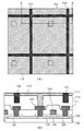
図1を用いて本実施形態を説明する。図1(A)は本実施形態の画素部の正面図であり、図1(B)は図1(A)の線A−A’で切った断面図である。
【0017】
図1(B)に示すように、基板100上には、画素毎にアクティブ素子としてTFTが形成されている。TFTはソース領域107、ドレイン領域108、チャネル形成領域109を有する活性層と、活性層を覆うゲイト絶縁膜102と、ゲイト電極105と、ソース電極111と、ドレイン電極113とを有する。
【0018】
これらTFTを覆って層間絶縁膜114が形成されている。層間絶縁膜114を介してTFTのドレイン電極113と画素電極115とが接続されている。層間絶縁膜114には隣接する画素電極115の隙間と重なる部分に溝部が形成されている。光吸収物122はこの溝部と画素電極115の隙間に埋め込まれ、図1(A)に示すように光吸収物122は一体的に格子状に設けられている。
【0019】
光吸収物122を形成するには、図5(A)に示すように、隣接する画素電極115の隙間と空隙が重なるように層間絶縁膜114をエッチング除去して、溝部120を形成する。画素電極115をエッチングマスクとして機能させることで、溝部120は自己整合的に形成され、画素電極115の端面(分断面)と層間絶縁膜114の溝部120の側面が概略同一平面をなすように形成される。
【0020】
次に図5(B)に示すように、層間絶縁膜114の溝部120および画素電極の隙間に埋め込まれ、かつ複数の画素電極115の表面を覆うように絶縁性の光吸収物121を形成する。次に、ドライエッチングやCMPの手段によって、画素電極115の表面を覆っている光吸収物121を除去して、図1に示すように複数の画素電極115の表面を露出させる。層間絶縁膜114の溝部および画素電極115の隙間に残存した部分が、図1の光吸収物122として機能する。
【0021】
本実施形態では、光吸収物122が形成される溝部は自己整合的に形成され、また光吸収物122のパターニング工程が不要なため、作製工程は簡単である。また光吸収物122は画素電極115の面積(開口率)を縮小することなく形成できる。
【0022】
本実施形態において、光吸収物122は少なくとも層間絶縁膜114に形成された溝部に存在させる。層間絶縁膜114の溝部の光吸収物122によって、画素部115の隙間から入射する光は吸収されて、反射したり透過したりしない。従って画素電極115を金属材料にて形成することにより、画素電極115と光吸収物122によって完全に光が遮蔽できるので、TFTの光劣化が防止でき、さらにクロストークも防止できる。
【0023】
層間絶縁膜114の溝部、および画素電極115の隙間に光吸収物122を埋め込むことにより、画素電極115の段差部が低くなる。例えば本発明の画素部を液晶パネルに応用した場合には、画素電極115の段差部での液晶分子の配向の乱れを抑制できる。より好ましくは画素電極115の表面と光吸収物122の表面を概略同一平面とする。これにより、基板間で液晶分子の配向状態が均一化され、ディスクリネーションが防止できる。
【0024】
また、光吸収物122を画素電極よりも突出させることもできる。これにより光吸収物112上に配置される液晶分子は画素電極115と対向電極が作る電界に応答しにくくなるので、表示に寄与する画素電極115上の液晶分子の応答を乱すことがなくなり、高画質表示が可能になる。
【0025】
光吸収物122は光を吸収する着色された絶縁材料で形成される。画素電極115の隙間の微細な溝部に充填されるため、光吸収物はスピンコート法で形成できる塗布膜が好適である。このような塗布膜として、アクリル、ポリイミド、ポリアミド、ポリイミドアミド、エポキシから選ばれた有機樹脂や、PSG、SiO2 等の酸化珪素系塗布膜を用いることができる。またこれら絶縁材料を着色するには、絶縁材料中に顔料やカーボン系材料を分散させる。
【0026】
【実施例】
以下、図1〜図8を用いて、本発明の実施例を詳細に説明する。
【0027】
[実施例1] 本実施例では、本発明を反射型液晶表示装置に応用した例を説明する。図1は本実施例の画素部の構成図であり、図1(A)は画素部の正面図であり、図1(B)は図1(A)の線A−A’で切った断面図である。
【0028】
図1に示す画素部において、絶縁表面を有する基板100上には画素毎にアクティブ素子としてTFTが形成されている。TFTを覆って層間絶縁膜114が形成されている。層間絶縁膜114を介してTFTのドレイン電極113と金属材料でなる画素電極115とが接続されている。層間絶縁膜114には、隣接する画素電極115の隙間に空隙が重なるように溝部が形成されている。この溝部と画素電極115の隙間に光吸収物122が埋め込まれている。
【0029】
図1(A)に示すように、画素電極115の隙間に光吸収物122は一体的に格子状に設けられ、画素電極115の隙間から光が侵入するのを防止している。以下、図2〜図6を用いて、図1に示す画素部の作製工程を説明する。
【0030】
絶縁表面を有する基板100を用意する。基板100には、ガラス基板や石英基板が用いられる。ガラス基板を用いる場合は、その表面にNaイオン等の不純物の拡散を防止するための酸化珪素でなる下地絶縁膜を形成すると良い。
【0031】
基板100上に画素毎にTFTの活性層101を形成する。活性層101を形成するには厚さ40〜100nm、ここでは厚さ50nmの非晶質シリコンを成膜し、多結晶化し、この多結晶化されたシリコンを島状に分離し活性層101を形成する。そして、しきい値制御のために活性層101にボロンをドーピングする。次に基板全体にゲイト絶縁膜102として機能する酸化珪素膜を成膜する。酸化珪素膜の厚さは120nmとする。
【0032】
ゲイト絶縁膜102上に、ゲイト電極・配線を構成する導電膜を形成する。本実施例では、Scを微量に添加したアルミニウム膜を400nmの厚さに形成する。アルミニウム膜をパターニングして、ゲイト電極104、ゲイト配線105を形成する。ゲイト電極104はゲイト配線105と一体的に形成され、配線105から延在した構成とされる。
【0033】
ゲイト電極・配線104、105を陽極とした陽極酸化処理を施し、その表面に陽極酸化膜106を形成する。この陽極酸化膜106はゲイト電極・配線104、105を電気的に物理的に保護する機能を有する。なお、図2(A)では陽極酸化膜106は省略されている。
【0034】
次に、イオンドーピング法にて、リンイオンを活性層101にドープする。ゲイト電極104がマスクになるため、ソース領域107、ドレイン領域108、チャネル形成領域109が自己整合的に形成される。ドーピング終了後、レーザ照射または熱処理によって、ドーピングされたリンを活性化すると同時に、ドーピングによって損傷した活性層をアニールする。
【0035】
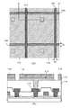
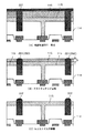
なお、図2(A)は画素部の上面図であり、図2(B)は図2(A)の線A−A’で切った断面図である。以降の工程を図3を用いて説明する。図3(A)は画素部の上面図であり、図3(B)は図3(A)の線A−A’で切った断面図である。
【0036】
図3(B)に示すように、第1の層間絶縁膜110を成膜する。ここでは、プラズマCVD法により厚さ20nmの窒化珪素膜を成膜し、連続して、厚さ800nmの窒化酸化珪素膜を成膜する。そして、層間絶縁膜110にソース/ドレイン領域107、108に達するコンタクトホールを開口する。
【0037】
次に、チタン膜/アルミニウム膜/チタン膜でなる積層膜を成膜する。各チタン膜の厚さは100nmとし、アルミニウム膜の厚さは300nmとする。この積層膜をパターニングしてソース電極111、ソース配線112、ドレイン電極113をそれぞれ形成する。ソース電極111はソース配線112と一体的に形成され、配線112から延在した構成とされる。以上の工程により、画素部のTFTが完成する。
【0038】
以降の工程を図4を用いて説明する。図4(A)は画素部の上面図であり、図4(B)は図4(A)の線A−A’で切った断面図である。
【0039】
図4(B)に示すように、TFTを覆う厚さ1〜2μmの第2の層間絶縁膜114を形成する。ここでは、層間絶縁膜114として厚さ1.5μmのアクリル膜を形成する。
【0040】
層間絶縁膜114の材料には有機樹脂膜が好ましい。有機樹脂膜はスピンコート法にて溶液を塗布することで成膜できるため、下部の凹凸を相殺して、表面が平坦な膜に成膜することができる。有機樹脂膜として、具体的には、アクリル、ポリイミド、ポリアミド、ポリイミドアミド、エポキシ等が用いられる。また、有機樹脂の他に塗布膜として、PSG、SiO2 等の酸化珪素系塗布膜を用いることができる。
【0041】
層間絶縁膜114にドレイン電極113に達するコンタクトホールを開口する。次に、画素電極115を構成する金属膜を成膜する。アルミニウム膜を厚さ200〜400nm、ここでは厚さ300nmにスパッタ法にて成膜する。次にアルミニウム膜上にパターニング用のレジストマスク116を形成する。このマスク116を用いてアルミニウム膜をパターニングし、画素電極115を形成する。なお、図4(A)においては、レジストマスク116は省略されている。
【0042】
各画素電極115は画素毎にTFTのドレイン電極113に接続され、またX方向、Y方向それぞれ間隔Px、Pyを隔てて、マトリクス状に配置されている。間隔Px、Pyは開口率が最大になるようなデザインルールのみに従って設定すれば良く、間隔Px、Pyは1〜3μm程度とすることができる。ここでは間隔Px、Pyを2μmとする。
【0043】
次に、図5に示すように、画素電極115をエッチングマスクに用いて、第2の層間絶縁膜114に溝部120を自己整合的に形成する。溝部120を形成するには、プラズマエッチングやRIE(反応性イオンエッチング)等のドライエッチング法を用いる。本実施例では、プラズマエッチング法を用い、エッチングガスは、O2 とCF4 の混合ガスを用いる。CF4 の濃度は全ガスに対して1〜10%とする。CF4 の濃度、圧力等の条件によりエッチングレートが制御できる。またエッチングガスによって、画素電極115の表面が変質されないようにするため、画素電極115の保護するためレジストマスク116は残存させてエッチングを行う。
【0044】
ここではCF4 の濃度が5%のエッチングガスを用い、プラズマエッチングによって、画素電極115の隙間の第2の層間絶縁膜114を深さ約1μm除去し、溝部120を形成する。図5(A)の断面図では溝部120は個々に分離されているように図示されているが、実際には、溝部120は画素電極115の隙間に重なるように、格子状に一体的に形成される。
【0045】
次に図5(B)に示すように、レジストマスク116を剥離した後、溝部120、隣接する画素電極115の隙間に充填され、かつ画素電極115表面を覆う絶縁物層121を形成する。本実施例では、スピンコート法にて黒色顔料を分散させたアクリル樹脂を塗布し硬化して、黒色のアクリルでなる絶縁物層121を形成する。
【0046】
溝部120の深さは1μmであり、またその幅は2μmである。このような微細な格子状のパターンを画素部全体で絶縁物層121によって充填するため、絶縁物層121は溶液から形成できる塗布膜を用いる。このような塗布膜としてアクリル、ポリイミド、ポリアミド、ポリイミドアミド、エポキシ等の有機樹脂が用いられる。本実施例で用いたアクリルは液晶材料よりも比誘電率が低く、列記した樹脂材料のなかで最も安価であるという特長がある。また溶液から形成できる膜として、PSG、SiO2 等の酸化珪素系塗布膜を用いることができる。
【0047】
また、絶縁物層121に、従来のブラックマトリクスと同様の遮光機能を持たせるため、黒色顔料を分散させたが、カーボン系材料を分散させることもできる。また顔料は黒色に限定されるものではなく、絶縁物層121が光を吸収できるような色であれば良い。
【0048】
次に、O2 アッシング等のドライエッチング処理により、画素電極115表面を覆う絶縁物層121を除去して、図1(B)に示すように隣接する画素電極115の隙間、および溝部120のみ絶縁物層121を残す。残存された絶縁物層121が光吸収物122となる。図1(B)では光吸収物は個々に分離されて図示されているが、実際には図1(A)に示すように光吸収物122は画素電極115の隙間を埋めて、格子状に一体的に形成される。
【0049】
本実施例では光吸収物122を形成する手段にO2 アッシングを用いる。アッシングのエッチングレートは代表的には0.3〜1μm/分程度であることを考慮すると、図5(B)において、画素電極115を覆う絶縁物層121の厚さt1が0.3〜1.5μm程度となるようにする。t1 の厚さは、絶縁物層121を形成する際のスピナ−の回転速度や、絶縁物層121の原料溶液の粘度等により制御できる。
【0050】
更に、画素電極121の反射率を損なわないようにするため、O2 アッシングでは画素電極115表面を覆う絶縁物層121を完全に除去する必要がある。画素電極115表面を覆う絶縁物層121を完全に除去される以前に、少なくとも溝部120に埋め込まれた絶縁物層121(後の光吸収物122となる部分)が除去されないようにするため、画素電極115の厚さと溝部120深さを加算した厚さt0 、即ち光吸収物122の厚さt0 は、アッシングされる絶縁物層121の厚さt1 よりも厚くする。これによってエッチングのマージンが確保でき、画素電極115の隙間および溝部120に埋め込まれた絶縁物層121を除去しないようすることができる。
【0051】
図5(B)において、t0 は溝部120の深さ1μmと、画素電極の厚さ300nmを加算した値の1.3μmであり、ここでは除去される絶縁物層121の厚さt1 は0.5μmとした。
【0052】
なおここでは、溝部120は層間絶縁膜114に凹状に形成したが、深さt0を稼ぐため層間絶縁膜114を貫通するように形成してもよい。この場合は、溝部120はゲイト配線105、ソース配線112が成す格子(図4参照)に沿って形成されるので、層間絶縁膜114を貫通するとソース配線112表面がエッチングガスに曝される。この場合には、ソース配線112表面はエッチングガスによって変質されない材料であることが必要である。
【0053】
また画素電極の間隔Px、Pyは1〜3μm程度であるので、アッシング工程において、画素電極115の隙間にはプラズマが殆ど入り込まず、この箇所の絶縁物層121は除去され難い。そのためアッシングによって、画素電極115の表面に形成された絶縁物層121は除去して、画素電極115の隙間および溝部120に埋め込まれた絶縁物層121を残存させることが可能である。この残存した絶縁物層121が図1の光吸収物122に相当する。
【0054】
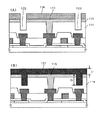
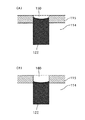
なお、図1では、光吸収物122の表面と画素電極115が一致するように図示されているが、上記したようにO2アッシングでは画素電極115表面を覆う絶縁物層121を完全に除去する必要がある。このため、図6(A)において、150で示すように、画素電極115の隙間の絶縁物層121が一部除去される場合もある。しかし図6(A)のように、光吸収物122の表面が画素電極115の表面よりも低くなっていても、画素電極115の隙間を通過する光は光吸収物122によって遮光できる。
【0055】
即ち、画素電極115の隙間を通過する光を遮光するためには、少なくとも溝部120の側面および底面を光吸収物122によって被覆すればよい。従って、画素電極115表面を覆う絶縁物層121を完全に除去するために、図6(B)において160で示すように、画素電極115の隙間の絶縁物層121を殆ど除去してもよい。
【0056】
光吸収物122を形成し図1に示す画素部が完成した後、公知のセル組工程により反射型液晶表示装置を完成する。なお液晶材料は常誘電性液晶、もしくは強誘電性液晶、反強誘電性液晶等表示モードに合わせて適宜に選択する。
【0057】
本実施例では光吸収物122は黒色顔料が分散されたアクリルで構成されているため、その表面で光が乱反射することがない。よって表示に寄与する光は画素電極115で反射された光だけとなるので、コントラストの高い表示が行える。
【0058】
また、光吸収物122を光が透過することがなく、画素電極115の材料は金属であるため、画素電極115と光吸収物112によって、TFTに光が照射されることが完全に防止できるので、光劣化が防止できる。
【0059】
また、光吸収物122を画素電極115の隙間にも埋め込むことにより、画素電極115の段差を緩和できる。この結果、画素電極115の段差部での液晶分子の配向の乱れを抑制できる。この効果は反射型表示装置だけでなく、透過型表示装置でも得ることができる。なお、透過型表示装置の場合は、光吸収物122の他に、TFTの活性層を遮光するブラックマトリクスを形成する必要がある。
【0060】
また本実施例では、光吸収物122が埋め込まれる溝部は自己整合的に形成され、また光吸収物122はパターニング工程が不要なため、工程が簡略化できる。更に開口率を損なうことなく形成できる。
【0061】
[実施例2] 実施例1では、光吸収物122を形成する際に、画素電極115表面を覆う余分な絶縁物層121を除去する手段として、ドライエッチング法を用いた。本実施例では、余分な絶縁物層121を除去する手段にCMP(化学的機械的研磨)を用いる。
【0062】
先ず、実施例1と同様の工程に従って、図5(B)に示す構造を作製する。そしてCMPによって、画素電極115表面を覆う余分な絶縁物層121を研磨し除去する。CMPの条件は絶縁物層121は研磨するが画素電極115をできるだけ研磨しないように、スラリの種類や研磨布の回転数を設定することで、画素電極115表面が露出したときにCMPを終了させることが可能である。
【0063】
このため、画素電極115表面の硬度と絶縁物層121の硬度差ができるだけ大きくなるようにする。例えば、実施例1のようにアルミニウム材料で画素電極115を形成した場合、その表面を陽極酸化処理等によって酸化してアルミナを形成すればよい。
【0064】
[実施例3] 図7は本実施例の光吸収物の作製工程の説明図である。本実施例では、光吸収物の他の作製方法を説明する。図8ではTFTを一部のみを図示した。また、図7において図1〜図5と同じ符号は同じ部材を示す。
【0065】
先ず、実施例1と同様の工程に従って、図5(A)に示す構造を作製する。そして、図7(A)に示すように画素電極115のパターニング用のレジストマスク116を残存させた状態で、絶縁物層201を形成する。この絶縁物層201は後に光吸収物を構成するものであり、着色された絶縁物材料でなる。
【0066】
本実施例でも実施例1と同様に、絶縁物層201をスピンコート法にて黒色顔料を分散させたアクリル樹脂を塗布し、硬化して、黒色のアクリルで形成する。これは、溝部120および画素電極115の隙間を絶縁物層201によって充填するためである。アクリル樹脂の他、スピンコート法で作成可能なポリイミド、ポリアミド、ポリイミドアミド、エポキシ等の有機樹脂や、PSG、SiO2 等の酸化珪素系塗布膜を用いることが可能である。なお絶縁物層201には黒色顔料を分散させたが、カーボン系材料を分散させることもできる。
【0067】
次に、O2 アッシング等のドライエッチング処理により、画素電極115表面を覆う絶縁物層201を除去する。エッチングを継続し、レジストマスク116と共にこの隙間に充填されていた絶縁物層201も除去する。そしてレジストマスク116が厚さh程残存した状態でエッチングを終了する。厚さhはエッチング時間により制御できる。
【0068】
図7(B)の状態で、溝部120、画素電極115の隙間、レジストマスク116の隙間に充填された絶縁物層201が残存する。これが光吸収物202となる。そして、図7(C)に示すように、専用の剥離液によってレジストマスク116のみを剥離する。この結果、画素電極115表面から突出して、光吸収物202が形成される。
【0069】
光吸収物202を画素電極115表面突出させることにより、光吸収物202上に(画素電極115の隙間上に)存在する液晶分子は近傍の画素電極115が作る電界の作用がおよび難く、応答させないようにできる。画素電極115の間に存在する液晶分子は表示に寄与しないため、このような液晶分子を応答させないことにより、画素電極115上に存在する液晶分子の応答不良が防止でき、高画質表示が可能になる。
【0070】
また図7に示す工程では、絶縁物層201とレジストマスク116のエッチングレートがほぼ同じ、もしくは絶縁物層201のエッチングレートが高い場合に特に有効であり、レジストマスク116を厚さhだけ残すことで、光吸収物202を画素電極115から突出させることができる。
【0071】
一方絶縁物層201よりもレジストマスク116のエッチングレートが高くなるように双方の材料を選択することも可能である。この場合にはレジストマスク116を完全に除去するまでエッチングを行う。エッチングが終了した時点では、エッチングレートの差により絶縁物層201が画素電極115の表面よりも突出して残存させることができる。また、レジストマスク116が完全に除去されたか否かはエッチング装置にてモニタリング可能であるが、レジストマスク116を残存させる厚さhは時間で制御しており、モニタリング不可能なので、完全に除去するほうがレジストマスク116を残存させてエッチングを終了させるよりも制御性・再現性に優れる。
【0072】
また、本実施例では光吸収物202を画素電極115表面よりも突出させるようにしたが、エッチング時間を延長してレジストマスク116を完全に除去し、光吸収物202の表面が画素電極115表面とほぼ同じになるようにすることもできる。また図6において150、160で示すように、画素電極115表面よりも陥没した状態までエッチングしても良く、光吸収物202を少なくとも層間絶縁膜114の溝部120に残存させればよい。
【0073】
あるいは図7(A)の構造まで作製した後、実施例2で説明したCMP工程によって、光吸収物202を形成することもできる。この場合、絶縁物層201と共にレジストマスク116も研磨除去して、画素電極115表面を露出させればよい。
【0074】
なお、実施例1〜3において画素部のアクティブ素子はトップゲイト型のTFTにしたが、この構造に限定されるものではなく、ボトムゲイト型TFT等の他の構造のTFTでもよい。またTFTに限らず、ダイオード、MIM素子等を形成することができる。
【0075】
また、実施例1〜3では基板100に絶縁性のガラスや石英を用いたが、反射型の画素部を形成する場合は単結晶シリコン基板を用いることができる。この場合には、アクティブマトリクス素子として、単結晶シリコン基板にMOS型トランジスタを形成すればよい。単結晶シリコン基板を用いることにより、画素電極115と光吸収物122によって基板表面からの光が遮蔽されると共に、基板裏面からの光も遮蔽できる。
【0076】
[実施例4] 図8は本実施例の電子機器の概略外観図である。本実施例では、本発明の電子機器の応用製品を説明する。本発明を応用した電子機器として、ビデオカメラ、スチルカメラ、プロジェクタ、ヘッドマウントディスプレイ、カーナビゲイション、パーソナルコンピュータ、携帯情報端末(モバイルコンピュータ、携帯電話)等が挙げられる。
【0077】
図8(A)はモバイルコンピュータ(モービルコンピュータ)であり、本体2001、カメラ部2002、受像部2003、操作スイッチ2004、反射型液晶表示装置2005で構成される。
【0078】
図8(B)はヘッドマウントディスプレイであり、本体2101、一対の反射型液晶表示装置2102、本体を頭部に固定するためのバンド部2103で構成される。一対の液晶表示装置は左眼用の画像、右眼用の画像をそれぞれ表示される。使用者はこの画像を光学系を介して視覚する。すると目前に大画面が表示されているように視覚することができる。
【0079】
図8(C)は携帯電話であり、本体2201、音声出力部2202、音声入力部2203、反射型液晶表示装置2204、操作スイッチ2205、アンテナ2206で構成される。
【0080】
図8(D)はビデオカメラであり、本体2301、反射型液晶表示表示装置2302、音声入力部2303、操作スイッチ2304、バッテリー2305、受像部2306で構成される。
【0081】
図8(E)はリア型プロジェクタであり、本体2401内部に配置された光源2402から出射した光は、反射型液晶表示装置2403の画素部で反射・変調される。この反射光は偏光ビームスプリッタ2504、リフレクタ2505、2506を経て、スクリーン2507に投影され、画像として表示される。
【0082】
図8(A)〜(E)に示す電子機器において、反射型液晶表示装置2005、2102、2202、2302、2403には、本発明の画素部が設けられ、またこの画素部を制御するための周辺駆動回路も画素部と同一基板上に形成されている。また、液晶材料は強誘電性液晶、反強誘電性液晶等、表示モードに合わせて適宜に選択する。
【0083】
本発明の画素部の構造によって、アクティブ素子の光劣化が防止されるため、長寿命化、信頼性の向上が図れる。特に、図8(E)のリア型プロジェクタのように強い光を照射する電子機器に非常に有効である。
【0084】
また、画素電極以外の反射光が無くなるため、高コントラストの高い、高画質表示が実現できる。この効果は、図8(E)のリア型プロジェクタのように、画像を数十〜数百倍にも拡大投影するような電子機器に非常に有効である。
【0085】
また、光吸収物によって画素電極の段差を平坦化もしくは緩和されているため、段差部での液晶分子の配向の乱れが無くなり、この配向の乱れによって生じていたコントラストの低下、特に黒表示の低下をなくすことができる。
【0086】
液晶分子の配向の乱れを防止する効果は、セルギャップが2〜4μm程度の反射型液晶表示装置や、セルギャップが2μm以下の強誘電性液晶・反強誘電性液晶表示装置に特に有効である。更に、図8(E)に示すプロジェクタは画素数が多く、その面積が微細なので、配向の乱れを防止することは画質の向上に非常に効果的である。プロジェクタの他の構成を図8(F)に示す。
【0087】
図8(F)はフロント型プロジェクタであり、本体2501において、光源2502からの光は透過型液晶表示装置2503で変調されて透過する。この透過光は光学系2504によってスクリーン2505に投影され、画像が表示される。本発明の画素部が透過型表示装置2503に用いられており、高精細な表示が実現できる。
【0088】
なお実施例1〜4では、液晶表示装置について説明したが、本発明の画素部はEL表示装置等の他のアクティブマトリクス型表示装置に応用でき、光吸収物により画素部のアクティブ素子の光劣化を防止できる。
【0089】
【発明の効果】
本発明においては、画素電極の隙間に形成される溝部に光吸収物を埋め込んだことにより、画素電極の隙間から光が入射することを完全に防止することができる。特に、画素電極を金属膜で構成することによって、画素電極と光吸収物にて光を完全に遮光できるため、アクティブ素子の光劣化を防止したり、クロストークを防止することができる。
【0090】
また、本発明の光吸収物が埋め込まれる溝部は自己整合的に形成され、更に光吸収物のパターニング工程が不要なため、製造方法が簡略化され、また画素領域の開口率を損なうことなく形成することができる。
【図面の簡単な説明】
【図1】 実施例1の画素部の正面図と断面図。
【図2】 実施例1の画素部の作製工程を説明するための正面図と断面図。
【図3】 実施例1の画素部の作製工程を説明するための正面図と断面図。
【図4】 実施例1の画素部の作製工程を説明するための正面図と断面図。
【図5】 実施例1の画素部の作製工程を説明するための断面図。
【図6】 実施例1の光吸収物の作製工程を説明するための溝部の拡大図。
【図7】 実施例3の画素部の作製工程を説明するための断面図。
【図8】 実施例4の電子機器の応用製品の説明図。
【図9】 従来例の画素部の正面図と断面図。
【符号の説明】
100 基板
101 活性層
102 ゲイト絶縁膜
104 ゲイト電極
105 ゲイト配線
107 ソース領域
108 ドレイン領域
109 チャネル形成領域
110 第1の層間絶縁膜
111 ソース電極
112 ソース配線
113 ドレイン電極
114 第2の層間絶縁膜
115 画素電極
116 レジストマスク
120 溝部
121 絶縁物層
122 光吸収物
201 絶縁物層
202 光吸収物[0001]
BACKGROUND OF THE INVENTION
The present invention relates to an active matrix panel having a pixel portion having a plurality of pixel electrodes, an electronic device such as a mobile phone or a personal computer provided with the pixel portion, and a manufacturing method thereof.
[0002]
[Prior art]
In information systems, flat displays such as liquid crystal panels that convert electric signals (image signals) into optical signals for display are drawing attention. In order to perform full color display or moving image display, a matrix driving method is adopted as a display method of these flat displays.
[0003]
FIG. 9 shows a cross-sectional view of a pixel portion of a conventional reflective active matrix liquid crystal display. FIG. 9 corresponds to a cross-sectional view of a so-called TFT substrate. A thin film transistor (TFT) 2 is formed for each pixel on a substrate 1 having an insulating surface. The
[0004]
The
[0005]
Through steps such as alignment film formation and rubbing treatment, the substrate on which the counter electrode is formed and the element substrate shown in FIG. 9 are bonded together. A liquid crystal material is sealed between the substrates, and the cell set of the reflective liquid crystal display device is completed.
[0006]
In FIG. 9, the
[0007]
[Problems to be solved by the invention]
In recent years, in the market of display devices such as HDTV (high-definition television), SXGA display, and photographic negative reading device, there has been a demand for a larger number of pixels and a higher density. However, as the pixel pitch is miniaturized, the ratio of the gap between the adjacent pixel electrodes becomes relatively wide, so the problem due to the gap between the pixel electrodes cannot be ignored.
[0008]
The first problem due to the gap between the pixel electrodes is that, in the reflective panel of the conventional example of FIG. 9, the
[0009]
Second, in the case of a liquid crystal display device, the alignment of liquid crystal molecules is disturbed at the stepped portion of the
[0010]
However, the cell gap of the reflective liquid crystal panel is about 2 to 4 μm, and the cell gap of the ferroelectric / antiferroelectric liquid crystal panel is 2 μm or less to solve the spiral of liquid crystal molecules, which is very narrow compared to the transmissive type. . Therefore, in these liquid crystal panels, since the ratio of the step difference in the cell gap is increased, the influence of the disturbance of the liquid crystal molecules is increased, which causes a decrease in contrast.
[0011]
An object of the present invention is to solve the above-described problems, and provide an electronic device including a pixel portion that has a long life and high reliability and can display a high image quality, and a manufacturing method thereof.
[0012]
[Means for Solving the Problems]
The configuration of the electronic device of the present invention for solving the above-described problem includes a plurality of active elements, an insulating layer covering the plurality of active elements, and a plurality of pixel electrodes formed on the insulating layer. An electronic device having a pixel region arranged,
The insulator layer is provided with a groove portion having a gap that overlaps a gap between the adjacent pixel electrodes,
An electronic device, wherein an insulating light absorber is embedded in the groove, or a gap between the groove and the adjacent pixel electrode.
[0013]
In addition, in the configuration of the method for manufacturing an electronic device according to the invention, a plurality of active elements, an insulating layer covering the plurality of active elements, and a plurality of pixel electrodes formed on the insulating layer are arranged. A method for manufacturing an electronic device having a pixel region,
A first step of forming the plurality of pixel electrodes on the insulator layer;
A second step of removing the insulator layer existing in the gap between the adjacent pixel electrodes to form a groove;
A third step of forming an insulating light absorber embedded in the groove;
It is characterized by having.
[0014]
Another structure of the method for manufacturing an electronic device of the present invention is as follows:
A first step of forming the plurality of pixel electrodes on the insulator layer;
Removing the insulating layer present in the gap between the adjacent pixel electrodes to form a groove, and after the second step, embedded in the gap between the groove and the pixel electrode; And a third step of forming an insulating light absorber covering the surface of the plurality of pixel electrodes, and removing the light absorber covering at least the surface of the plurality of pixel electrodes to expose the surface of the pixel electrode. And a fourth step.
[0015]
Furthermore, another structure of the method for manufacturing an electronic device of the present invention is as follows:
Forming a plurality of pixel electrodes by forming a conductive film on the insulator layer, forming a resist mask on the conductive film, and patterning the conductive film;
A second step of forming a groove by removing the insulator layer existing in a gap between the adjacent pixel electrodes in a state where the resist mask is left;
A third step of forming an insulating light absorber embedded in the gap between the groove and the pixel electrode and covering the resist mask surface;
A fourth step of removing the insulating light absorber covering at least the resist mask surface and the resist mask to expose the pixel electrode surface;
A method for manufacturing an electrode structure comprising:
[0016]
DETAILED DESCRIPTION OF THE INVENTION
This embodiment will be described with reference to FIG. 1A is a front view of the pixel portion of this embodiment, and FIG. 1B is a cross-sectional view taken along line AA ′ in FIG.
[0017]
As shown in FIG. 1B, a TFT is formed on the
[0018]
An interlayer insulating
[0019]
In order to form the
[0020]
Next, as shown in FIG. 5B, an insulating
[0021]
In the present embodiment, the groove in which the
[0022]
In the present embodiment, the
[0023]
By embedding the
[0024]
Further, the
[0025]
The
[0026]
【Example】
Hereinafter, embodiments of the present invention will be described in detail with reference to FIGS.
[0027]
[Embodiment 1] In this embodiment, an example in which the present invention is applied to a reflective liquid crystal display device will be described. FIG. 1 is a configuration diagram of a pixel portion of this embodiment, FIG. 1A is a front view of the pixel portion, and FIG. 1B is a cross section taken along line AA ′ in FIG. FIG.
[0028]
In the pixel portion shown in FIG. 1, a TFT is formed as an active element for each pixel on a
[0029]
As shown in FIG. 1A,
[0030]
A
[0031]
A TFT
[0032]
A conductive film constituting a gate electrode / wiring is formed on the
[0033]
Anodizing is performed using the gate electrodes /
[0034]
Next, phosphorus ions are doped into the
[0035]
2A is a top view of the pixel portion, and FIG. 2B is a cross-sectional view taken along line AA ′ in FIG. 2A. The subsequent steps will be described with reference to FIG. 3A is a top view of the pixel portion, and FIG. 3B is a cross-sectional view taken along line AA ′ in FIG. 3A.
[0036]
As shown in FIG. 3B, a first
[0037]
Next, a laminated film of titanium film / aluminum film / titanium film is formed. The thickness of each titanium film is 100 nm, and the thickness of the aluminum film is 300 nm. The stacked film is patterned to form a
[0038]
The subsequent steps will be described with reference to FIG. 4A is a top view of the pixel portion, and FIG. 4B is a cross-sectional view taken along line AA ′ in FIG. 4A.
[0039]
As shown in FIG. 4B, a second
[0040]
The material of the
[0041]
A contact hole reaching the
[0042]
Each
[0043]
Next, as shown in FIG. 5, the
[0044]
Here CF Four Using an etching gas with a concentration of 5%, the second
[0045]
Next, as shown in FIG. 5B, after the resist
[0046]
The depth of the
[0047]
Further, the black pigment is dispersed in order to give the
[0048]
Next, O 2
[0049]
In this embodiment, the means for forming the
[0050]
Further, in order not to impair the reflectance of the
[0051]
In FIG. 5B, t 0 Is 1.3 μm, which is the sum of the depth of the
[0052]
Here, the
[0053]
Further, since the pixel electrode intervals Px and Py are about 1 to 3 μm, plasma hardly enters the gaps between the
[0054]
In FIG. 1, the surface of the
[0055]
That is, in order to block light passing through the gap between the
[0056]
After the
[0057]
In this embodiment, since the
[0058]
Further, since light does not pass through the
[0059]
Further, the step of the
[0060]
In this embodiment, the groove in which the
[0061]
[Example 2] In Example 1, when the
[0062]
First, the structure shown in FIG. 5B is manufactured according to the same steps as in the first embodiment. Then, the excess insulating
[0063]
For this reason, the
[0064]
Example 3 FIG. 7 is an explanatory diagram of a manufacturing process of a light absorber according to this example. In this example, another method for manufacturing a light absorber is described. FIG. 8 shows only a part of the TFT. In FIG. 7, the same reference numerals as those in FIGS. 1 to 5 denote the same members.
[0065]
First, the structure shown in FIG. 5A is manufactured according to the same steps as in the first embodiment. Then, as illustrated in FIG. 7A, the insulating
[0066]
Also in this embodiment, as in the first embodiment, the insulating
[0067]
Next, O 2
[0068]
In the state of FIG. 7B, the insulating
[0069]
By causing the
[0070]
In the step shown in FIG. Resist mask This is particularly effective when the etching rate of 116 is substantially the same or when the etching rate of the insulating
[0071]
On the other hand, both materials can be selected so that the etching rate of the resist
[0072]
In this embodiment, the
[0073]
Alternatively, after the structure shown in FIG. 7A is manufactured, the
[0074]
In the first to third embodiments, the active element in the pixel portion is a top gate type TFT, but is not limited to this structure, and may be a TFT having another structure such as a bottom gate type TFT. In addition to a TFT, a diode, an MIM element, or the like can be formed.
[0075]
In Examples 1 to 3, although insulating glass or quartz is used for the
[0076]
Example 4 FIG. 8 is a schematic external view of an electronic apparatus of this example. In this embodiment, an application product of the electronic device of the present invention will be described. Examples of the electronic apparatus to which the present invention is applied include a video camera, a still camera, a projector, a head mounted display, a car navigation system, a personal computer, a personal digital assistant (mobile computer, mobile phone), and the like.
[0077]
FIG. 8A illustrates a mobile computer, which includes a
[0078]
FIG. 8B illustrates a head-mounted display which includes a main body 2101, a pair of reflective liquid
[0079]
FIG. 8C illustrates a mobile phone, which includes a
[0080]
FIG. 8D illustrates a video camera, which includes a
[0081]
FIG. 8E shows a rear projector, and light emitted from a light source 2402 disposed inside a
[0082]
In the electronic devices shown in FIGS. 8A to 8E, the reflective liquid
[0083]
With the structure of the pixel portion of the present invention, light degradation of the active element is prevented, so that the lifetime can be extended and the reliability can be improved. In particular, the present invention is very effective for an electronic apparatus that emits strong light such as the rear projector in FIG.
[0084]
In addition, since there is no reflected light other than the pixel electrodes, high-contrast and high-quality display can be realized. This effect is very effective for an electronic apparatus that projects an enlarged image several tens to several hundreds of times like the rear projector of FIG.
[0085]
In addition, since the step of the pixel electrode is flattened or relaxed by the light absorber, there is no disturbance in the alignment of the liquid crystal molecules at the step, and the contrast caused by this disturbance in alignment, particularly the black display, is reduced. Can be eliminated.
[0086]
The effect of preventing disorder of the alignment of liquid crystal molecules is particularly effective for a reflective liquid crystal display device having a cell gap of about 2 to 4 μm, and a ferroelectric liquid crystal / antiferroelectric liquid crystal display device having a cell gap of 2 μm or less. . Further, since the projector shown in FIG. 8E has a large number of pixels and a small area, preventing the disturbance of orientation is very effective for improving the image quality. Another structure of the projector is shown in FIG.
[0087]
FIG. 8F illustrates a front projector. In a
[0088]
In the first to fourth embodiments, the liquid crystal display device has been described. However, the pixel portion of the present invention can be applied to other active matrix display devices such as an EL display device, and light deterioration of the active elements in the pixel portion is caused by a light absorber. Can be prevented.
[0089]
【The invention's effect】
In the present invention, the light absorber is buried in the groove formed in the gap between the pixel electrodes, so that it is possible to completely prevent light from entering from the gap between the pixel electrodes. In particular, since the pixel electrode is made of a metal film, light can be completely blocked by the pixel electrode and the light absorber, so that the active element can be prevented from being deteriorated in light and crosstalk can be prevented.
[0090]
In addition, the groove in which the light absorber of the present invention is embedded is formed in a self-aligned manner, and further, the manufacturing method is simplified because the patterning process of the light absorber is unnecessary, and the aperture ratio of the pixel region is not impaired. can do.
[Brief description of the drawings]
FIGS. 1A and 1B are a front view and a cross-sectional view of a pixel portion of Embodiment 1. FIGS.
FIGS. 2A and 2B are a front view and a cross-sectional view for explaining a manufacturing process of a pixel portion of Embodiment 1. FIGS.
FIGS. 3A and 3B are a front view and a cross-sectional view for explaining a manufacturing process of a pixel portion of Embodiment 1. FIGS.
FIGS. 4A and 4B are a front view and a cross-sectional view for explaining a manufacturing process of a pixel portion of Embodiment 1. FIGS.
5 is a cross-sectional view illustrating a manufacturing step of a pixel portion of Example 1. FIG.
6 is an enlarged view of a groove for explaining a manufacturing process of the light absorber of Example 1. FIG.
7 is a cross-sectional view illustrating a manufacturing process of a pixel portion of Example 3. FIG.
FIG. 8 is an explanatory diagram of an application product of the electronic device of the fourth embodiment.
FIG. 9 is a front view and a cross-sectional view of a pixel portion of a conventional example.
[Explanation of symbols]
100 substrates
101 Active layer
102 Gate insulation film
104 Gate electrode
105 Gate wiring
107 Source region
108 Drain region
109 Channel formation region
110 First interlayer insulating film
111 Source electrode
112 Source wiring
113 Drain electrode
114 Second interlayer insulating film
115 pixel electrode
116 resist mask
120 groove
121 Insulator layer
122 Light absorber
201 Insulator layer
202 Light absorber
Claims (8)
前記第1の層間絶縁膜上に配線を形成し、
前記第1の層間絶縁膜上に、前記配線を覆う第2の層間絶縁膜を形成し、
前記第2の層間絶縁膜上に、前記配線と隣接する画素電極の隙間とが重なる位置になるように反射性を有する金属材料からなる複数の画素電極を形成し、
前記複数の画素電極をマスクとして、前記第2の層間絶縁膜を貫通し前記配線に達する溝部を形成し、
前記溝部に充填され且つ前記複数の画素電極表面を覆う絶縁層を形成した後にドライエッチング処理を行い前記複数の画素電極表面の絶縁層を除去することによって前記溝部に絶縁性の光吸収物を埋め込むことを特徴とする電子機器の作製方法。Forming a first interlayer insulating film covering the plurality of transistors;
Forming a wiring on the first interlayer insulating film;
Forming a second interlayer insulating film covering the wiring on the first interlayer insulating film;
On the second interlayer insulating film, a plurality of pixel electrodes made of a reflective metal material are formed so that the wirings and the gaps between adjacent pixel electrodes overlap each other.
Using the plurality of pixel electrodes as a mask, forming a trench that penetrates the second interlayer insulating film and reaches the wiring;
After forming an insulating layer filling the groove and covering the surface of the plurality of pixel electrodes, dry etching is performed to remove the insulating layer on the surface of the plurality of pixel electrodes , thereby embedding an insulating light absorber in the groove. A manufacturing method of an electronic device.
前記配線は、前記トランジスタと電気的に接続されるように形成されることを特徴とする電子機器の作製方法。In claim 1 ,
The method for manufacturing an electronic device is characterized in that the wiring is formed so as to be electrically connected to the transistor.
前記光吸収物は、顔料またはカーボン系材料が分散された有機樹脂を用いて形成されることを特徴とする電子機器の作製方法。According to claim 1 or claim 2,
The method of manufacturing an electronic device, wherein the light absorber is formed using an organic resin in which a pigment or a carbon-based material is dispersed.
前記光吸収物は、顔料またはカーボン系材料が分散された酸化珪素系塗布膜を用いて形成されることを特徴とする電子機器の作製方法。According to claim 1 or claim 2,
The method of manufacturing an electronic device, wherein the light absorber is formed using a silicon oxide-based coating film in which a pigment or a carbon-based material is dispersed.
前記有機樹脂は、アクリル,ポリイミド、ポリアミド、ポリイミドアミド、エポキシから選ばれた材料であることを特徴とする電子機器の作製方法。In claim 3 ,
The method for manufacturing an electronic device, wherein the organic resin is a material selected from acrylic, polyimide, polyamide, polyimide amide, and epoxy.
前記第2の層間絶縁膜は、有機樹脂を用いて形成されることを特徴とする電子機器の作製方法。In any one of Claims 1 thru | or 5 ,
The method for manufacturing an electronic device, wherein the second interlayer insulating film is formed using an organic resin.
前記第2の層間絶縁膜は、酸化珪素系塗布膜を用いて形成されることを特徴とする電子機器の作製方法。In any one of Claims 1 thru | or 5 ,
The method for manufacturing an electronic device, wherein the second interlayer insulating film is formed using a silicon oxide-based coating film.
前記第2の層間絶縁膜の有機樹脂は、アクリル,ポリイミド、ポリアミド、ポリイミドアミド、エポキシから選ばれた材料であることを特徴とする電子機器の作製方法。In claim 6 ,
The method for manufacturing an electronic device, wherein the organic resin of the second interlayer insulating film is a material selected from acrylic, polyimide, polyamide, polyimide amide, and epoxy.
Priority Applications (3)
| Application Number | Priority Date | Filing Date | Title |
|---|---|---|---|
| JP24050597A JP4105261B2 (en) | 1997-08-20 | 1997-08-20 | Manufacturing method of electronic equipment |
| US09/134,547 US6757032B1 (en) | 1997-08-20 | 1998-08-17 | Electronic device and method for fabricating the same |
| US10/848,146 US7145613B2 (en) | 1997-08-20 | 2004-05-19 | Electronic device and method for fabricating the same |
Applications Claiming Priority (1)
| Application Number | Priority Date | Filing Date | Title |
|---|---|---|---|
| JP24050597A JP4105261B2 (en) | 1997-08-20 | 1997-08-20 | Manufacturing method of electronic equipment |
Related Child Applications (1)
| Application Number | Title | Priority Date | Filing Date |
|---|---|---|---|
| JP2007127038A Division JP4057044B2 (en) | 2007-05-11 | 2007-05-11 | Manufacturing method of electronic equipment |
Publications (2)
| Publication Number | Publication Date |
|---|---|
| JPH1164890A JPH1164890A (en) | 1999-03-05 |
| JP4105261B2 true JP4105261B2 (en) | 2008-06-25 |
Family
ID=17060525
Family Applications (1)
| Application Number | Title | Priority Date | Filing Date |
|---|---|---|---|
| JP24050597A Expired - Fee Related JP4105261B2 (en) | 1997-08-20 | 1997-08-20 | Manufacturing method of electronic equipment |
Country Status (2)
| Country | Link |
|---|---|
| US (2) | US6757032B1 (en) |
| JP (1) | JP4105261B2 (en) |
Families Citing this family (16)
| Publication number | Priority date | Publication date | Assignee | Title |
|---|---|---|---|---|
| US7821065B2 (en) * | 1999-03-02 | 2010-10-26 | Semiconductor Energy Laboratory Co., Ltd. | Semiconductor device comprising a thin film transistor comprising a semiconductor thin film and method of manufacturing the same |
| JP2001109404A (en) * | 1999-10-01 | 2001-04-20 | Sanyo Electric Co Ltd | El display device |
| JP2002006321A (en) * | 2000-04-17 | 2002-01-09 | Seiko Epson Corp | Liquid crystal device, projection type display device and electronic equipment |
| JP4896318B2 (en) * | 2001-09-10 | 2012-03-14 | 株式会社半導体エネルギー研究所 | Method for manufacturing light emitting device |
| KR100552975B1 (en) * | 2003-11-22 | 2006-02-15 | 삼성에스디아이 주식회사 | active matrix OLED and fabrication method of the same |
| KR20060083247A (en) * | 2005-01-14 | 2006-07-20 | 삼성전자주식회사 | Thin film transistor array panel and manufacturing method thereof |
| JP4805587B2 (en) * | 2005-02-24 | 2011-11-02 | エーユー オプトロニクス コーポレイション | Liquid crystal display device and manufacturing method thereof |
| JP4552780B2 (en) * | 2005-07-04 | 2010-09-29 | エプソンイメージングデバイス株式会社 | Electro-optical device and electronic apparatus |
| JP5151782B2 (en) * | 2008-08-04 | 2013-02-27 | コニカミノルタホールディングス株式会社 | Manufacturing method of TFT array substrate |
| JP2010249935A (en) | 2009-04-13 | 2010-11-04 | Sony Corp | Display device |
| JP5262973B2 (en) * | 2009-05-11 | 2013-08-14 | セイコーエプソン株式会社 | Electro-optical device and electronic apparatus |
| KR102251729B1 (en) | 2009-07-31 | 2021-05-13 | 가부시키가이샤 한도오따이 에네루기 켄큐쇼 | Semiconductor device and manufacturing method thereof |
| JP2012220507A (en) * | 2011-04-04 | 2012-11-12 | Jvc Kenwood Corp | Liquid crystal display device and manufacturing method for the same |
| KR101860861B1 (en) * | 2011-06-13 | 2018-05-25 | 삼성디스플레이 주식회사 | Manufacturing method for wire, TFT and flat display device |
| JP6099891B2 (en) * | 2012-07-03 | 2017-03-22 | キヤノン株式会社 | Dry etching method |
| CN105572960A (en) * | 2016-03-02 | 2016-05-11 | 京东方科技集团股份有限公司 | Display substrate, liquid crystal panel, display device and manufacturing method of display substrate |
Family Cites Families (19)
| Publication number | Priority date | Publication date | Assignee | Title |
|---|---|---|---|---|
| US3428044A (en) * | 1965-10-15 | 1969-02-18 | Kimberly Clark Co | Coated catamenial tampon |
| US3595236A (en) * | 1969-03-17 | 1971-07-27 | Kimberly Clark Co | Coating to aid tampon insertion and tampons coated therewith |
| US3976075A (en) * | 1975-02-24 | 1976-08-24 | Personal Products Company | Tampon blank with reduced sloughing properties |
| JP2594983B2 (en) * | 1987-11-10 | 1997-03-26 | カシオ計算機株式会社 | Method for manufacturing thin film transistor |
| US5403300A (en) * | 1989-03-31 | 1995-04-04 | Smith & Nephew P.L.C. | Tampons |
| DE3940640A1 (en) * | 1989-12-08 | 1991-06-20 | Nokia Unterhaltungselektronik | METHOD FOR PRODUCING A SUBSTRATE PLATE FOR A LIQUID CRYSTAL CELL WITH BLACK MATRIX AREAS |
| JPH0444008A (en) * | 1990-06-12 | 1992-02-13 | Matsushita Electric Ind Co Ltd | Manufacture of liquid crystal element |
| JPH07294958A (en) * | 1994-04-26 | 1995-11-10 | Seiko Instr Inc | Semiconductor device for light valve and its production |
| JPH08122761A (en) * | 1994-10-20 | 1996-05-17 | Fujitsu Ltd | Liquid crystal display element and its production |
| US6424388B1 (en) * | 1995-04-28 | 2002-07-23 | International Business Machines Corporation | Reflective spatial light modulator array |
| JPH08327990A (en) * | 1995-05-29 | 1996-12-13 | Optrex Corp | Electrode substrate for liquid crystal display element and its production |
| JPH09105953A (en) * | 1995-10-12 | 1997-04-22 | Semiconductor Energy Lab Co Ltd | Liquid crystal display device |
| JP3332773B2 (en) * | 1996-03-15 | 2002-10-07 | シャープ株式会社 | Active matrix substrate and method of manufacturing active matrix substrate |
| JPH09281508A (en) * | 1996-04-12 | 1997-10-31 | Semiconductor Energy Lab Co Ltd | Liquid crystal display device and its manufacture |
| JP3587426B2 (en) * | 1996-09-25 | 2004-11-10 | シャープ株式会社 | Liquid crystal display device and method of manufacturing the same |
| CN1148600C (en) | 1996-11-26 | 2004-05-05 | 三星电子株式会社 | Liquid crystal display using organic insulating material and manufacturing methods thereof |
| JP3856889B2 (en) | 1997-02-06 | 2006-12-13 | 株式会社半導体エネルギー研究所 | Reflective display device and electronic device |
| US6163055A (en) | 1997-03-24 | 2000-12-19 | Semiconductor Energy Laboratory Co., Ltd | Semiconductor device and manufacturing method thereof |
| US6330047B1 (en) | 1997-07-28 | 2001-12-11 | Sharp Kabushiki Kaisha | Liquid crystal display device and method for fabricating the same |
-
1997
- 1997-08-20 JP JP24050597A patent/JP4105261B2/en not_active Expired - Fee Related
-
1998
- 1998-08-17 US US09/134,547 patent/US6757032B1/en not_active Expired - Fee Related
-
2004
- 2004-05-19 US US10/848,146 patent/US7145613B2/en not_active Expired - Fee Related
Also Published As
| Publication number | Publication date |
|---|---|
| US6757032B1 (en) | 2004-06-29 |
| US20040214359A1 (en) | 2004-10-28 |
| US7145613B2 (en) | 2006-12-05 |
| JPH1164890A (en) | 1999-03-05 |
Similar Documents
| Publication | Publication Date | Title |
|---|---|---|
| JP4105261B2 (en) | Manufacturing method of electronic equipment | |
| US5592318A (en) | Liquid crystal display apparatus having an inorganic filler between pixel electrodes and a method for producing the same | |
| JP3332773B2 (en) | Active matrix substrate and method of manufacturing active matrix substrate | |
| US5500750A (en) | Manufacturing method of reflection type liquid crystal display devices having light shield elements and reflective electrodes formed of same material | |
| KR100510566B1 (en) | In-plane switching mode liquid crystal display device | |
| KR100660578B1 (en) | Liquid crystal display apparatus | |
| US7202497B2 (en) | Semiconductor device | |
| US20040135952A1 (en) | Electro-optical device and electronic apparatus | |
| KR100697998B1 (en) | Semiconductor device and method of manufacturing the same, electro-optical device and method of manufacturing the same, and electronic apparatus | |
| TWI252363B (en) | Electro-optical device | |
| JPH11160735A (en) | Electro-optic device, production thereof and electronic equipment | |
| JPH09318972A (en) | Liquid crystal display device and its manufacture | |
| WO1995025291A1 (en) | Active matrix liquid crystal display device | |
| KR19980080689A (en) | Display device | |
| US7277150B2 (en) | Electrooptical device, method of manufacturing same, and electronic apparatus | |
| JP2000275680A (en) | Reflection type liquid crystal display device and display panel using the same | |
| JP4692699B2 (en) | Active matrix liquid crystal display device | |
| JPH10508387A (en) | Method of manufacturing reflective display | |
| JP4329445B2 (en) | Electro-optical device and electronic apparatus | |
| US7079198B2 (en) | Wiring structure, method of manufacturing the same, electro-optical device, and electronic device | |
| JP4057044B2 (en) | Manufacturing method of electronic equipment | |
| JP4096546B2 (en) | ELECTRO-OPTICAL DEVICE, MANUFACTURING METHOD THEREOF, AND ELECTRONIC DEVICE | |
| JP2011221158A (en) | Method for manufacturing liquid crystal device | |
| KR100455537B1 (en) | Liquid crystal display apparatus and projection-type liquid crystal display apparatus | |
| JPH10301145A (en) | Liquid crystal display device and electronic device |
Legal Events
| Date | Code | Title | Description |
|---|---|---|---|
| A521 | Written amendment |
Free format text: JAPANESE INTERMEDIATE CODE: A523 Effective date: 20040615 |
|
| A621 | Written request for application examination |
Free format text: JAPANESE INTERMEDIATE CODE: A621 Effective date: 20040615 |
|
| A977 | Report on retrieval |
Free format text: JAPANESE INTERMEDIATE CODE: A971007 Effective date: 20060316 |
|
| A131 | Notification of reasons for refusal |
Free format text: JAPANESE INTERMEDIATE CODE: A131 Effective date: 20070410 |
|
| A521 | Written amendment |
Free format text: JAPANESE INTERMEDIATE CODE: A523 Effective date: 20070514 |
|
| A131 | Notification of reasons for refusal |
Free format text: JAPANESE INTERMEDIATE CODE: A131 Effective date: 20071009 |
|
| A521 | Written amendment |
Free format text: JAPANESE INTERMEDIATE CODE: A523 Effective date: 20071024 |
|
| A02 | Decision of refusal |
Free format text: JAPANESE INTERMEDIATE CODE: A02 Effective date: 20071211 |
|
| A521 | Written amendment |
Free format text: JAPANESE INTERMEDIATE CODE: A523 Effective date: 20080109 |
|
| A911 | Transfer of reconsideration by examiner before appeal (zenchi) |
Free format text: JAPANESE INTERMEDIATE CODE: A911 Effective date: 20080215 |
|
| TRDD | Decision of grant or rejection written | ||
| A01 | Written decision to grant a patent or to grant a registration (utility model) |
Free format text: JAPANESE INTERMEDIATE CODE: A01 Effective date: 20080325 |
|
| A61 | First payment of annual fees (during grant procedure) |
Free format text: JAPANESE INTERMEDIATE CODE: A61 Effective date: 20080327 |
|
| R150 | Certificate of patent or registration of utility model |
Free format text: JAPANESE INTERMEDIATE CODE: R150 |
|
| FPAY | Renewal fee payment (event date is renewal date of database) |
Free format text: PAYMENT UNTIL: 20110404 Year of fee payment: 3 |
|
| FPAY | Renewal fee payment (event date is renewal date of database) |
Free format text: PAYMENT UNTIL: 20110404 Year of fee payment: 3 |
|
| FPAY | Renewal fee payment (event date is renewal date of database) |
Free format text: PAYMENT UNTIL: 20110404 Year of fee payment: 3 |
|
| FPAY | Renewal fee payment (event date is renewal date of database) |
Free format text: PAYMENT UNTIL: 20120404 Year of fee payment: 4 |
|
| FPAY | Renewal fee payment (event date is renewal date of database) |
Free format text: PAYMENT UNTIL: 20130404 Year of fee payment: 5 |
|
| FPAY | Renewal fee payment (event date is renewal date of database) |
Free format text: PAYMENT UNTIL: 20130404 Year of fee payment: 5 |
|
| FPAY | Renewal fee payment (event date is renewal date of database) |
Free format text: PAYMENT UNTIL: 20140404 Year of fee payment: 6 |
|
| R250 | Receipt of annual fees |
Free format text: JAPANESE INTERMEDIATE CODE: R250 |
|
| R250 | Receipt of annual fees |
Free format text: JAPANESE INTERMEDIATE CODE: R250 |
|
| R250 | Receipt of annual fees |
Free format text: JAPANESE INTERMEDIATE CODE: R250 |
|
| LAPS | Cancellation because of no payment of annual fees |