JP4095343B2 - Image processing device - Google Patents
Image processing device Download PDFInfo
- Publication number
- JP4095343B2 JP4095343B2 JP2002146344A JP2002146344A JP4095343B2 JP 4095343 B2 JP4095343 B2 JP 4095343B2 JP 2002146344 A JP2002146344 A JP 2002146344A JP 2002146344 A JP2002146344 A JP 2002146344A JP 4095343 B2 JP4095343 B2 JP 4095343B2
- Authority
- JP
- Japan
- Prior art keywords
- unit
- image
- data
- image data
- image processing
- Prior art date
- Legal status (The legal status is an assumption and is not a legal conclusion. Google has not performed a legal analysis and makes no representation as to the accuracy of the status listed.)
- Expired - Fee Related
Links
Images


Description
【0001】
【発明の属する技術分野】
本発明は、ファクシミリ(FAX)や複写機等に適用される画像処理装置に関する。
【0002】
【従来の技術】
一般的に、ファクシミリや複写機等における画像データの画像処理を実行する画像処理装置には、処理速度やコスト面で優位となるため、LSIやASIC等のハードウェアチップ(以下、LSI)が使用されることが多い。
【0003】
画像処理装置は、単に一つの画像処理手段だけではなく、複数の画像処理手段の組み合わせによって実現される複雑な画像処理を行うのが一般的である。ここで、画像処理手段とは例えば、濃度変換、フィルタ処理、拡大縮小処理、回転処理、等を行う手段である。そうしたことから、一つの画像処理を実現する単一機能のLSIを複数用意して、それらを直列に接続して使用することで、複数の画像処理の組み合わせによる複雑な画像処理を実現する画像処理装置が実現されることになる。組み合わせるLSIを様々に変えることで様々な複雑な画像処理装置を構成することが可能であり、少ないLSIを利用した低機能だが低コストの画像処理装置や、多くのLSIを利用した高コストだが高機能の画像処理装置等が用途に応じて構成することが可能である。
【0004】
ところが近年はLSIの集積度が向上し、一つのLSI内部に複数の画像処理手段を持ち、それらを組み合わせることで、一つのLSIだけの処理で複雑な画像処理が実行可能なLSIが登場している。こうした高集積度LSIを利用して画像処理装置を構成する方法は、画像処理装置のハードウェアが単純化されて品質面やコスト面で有利となるために、主流となりつつある。
【0005】
【発明が解決しようとする課題】
しかしながら、この少数の高集積度LSIで画像処理装置を構成する方法では、LSIの組み合わせによる柔軟性はなくなってしまうため、これまでは数多くのLSIの組み合わせを変えることで実現できていた柔軟な構成の変更が不可能となってしまう。そのために、高コストだが高機能な画像処理を実現するためには専用の大型高集積度LSIを開発し、また、低機能だが低コストな画像処理を実現するためには専用の小型高集積度LSIを開発する必要がある。また、ある一つの画像処理手段の内容だけを変更したいといった場合には、これまではその画像処理に対応するLSI一つだけを新たに開発し直せばよかったものが、すべての画像処理手段を含んだ高集積度LSI全体を新たに開発し直さなくてはならなくなり、開発コストの面で非常に不利になってしまう。また、高コストだが高機能な画像処理装置および低機能だが低コストな画像処理装置の両方に対して搭載可能な汎用的かつ高機能な高集積度LSIを開発することも可能であるが、LSIの規模が大きくなりすぎてコストの面で非常に不利となってしまう。
【0006】
本発明は上述した従来の技術の有するこのような問題点に鑑みてなされたものであり、その第1の目的とするところは、高集積度LSIを利用して少数のLSIで数多くの画像処理の組み合わせによる複雑な画像処理を実現する構成を取りながら、柔軟な構成の変更を可能にし、少ない構成変更の場合にLSI全体を作り直すことなく対応可能な、拡張性や流用性にも優れた画像処理装置を提供することにある。
【0007】
【課題を解決するための手段】
上記第1の目的を達成するために本発明は、画像データと、属性データとに基づいて当該画像データに対する画像処理を行う画像処理装置であって、
画像データ及び前記画像データを画像処理後プリンタ部へ転送するかファクシミリ送信するかに応じて決まるIDであって転送先のハードウエア手段を示すIDと画像処理の順序を示すIDを含む属性データの入出力を行う入力部及び出力部を有し、画像データに対して同じ種類の画像処理を行う画像処理部群を有する第1のハードウエア手段及び第2のハードウエア手段と、
画像データ及び属性データの入出力を行う入力部及び出力部を有し、前記属性データの値を指示する制御を行う制御手段とを有し、
前記第1のハードウエア処理手段と前記第2のハードウエア手段は直列に接続されるとともに、前記制御手段の出力部からの出力が前記第1のハードウエア手段の入力部に入力され、かつ前記第2のハードウエア手段の出力部からの出力が前記制御手段の入力部に入力されるように構成され、
前記第1のハードウエア手段は、入力部から入力された前記画像処理後プリンタ部へ転送するかファクシミリ送信するかに応じて決まるIDであって転送先のハードウエア手段を示すIDに基づいて、前記画像データに対して画像処理を内部で行う場合、前記画像処理の順序を示すIDにより決まる前記画像処理部群において処理を行い、入力部から入力された前記画像処理後プリンタ部へ転送するかファクシミリ送信するかに応じて決まるIDであって転送先のハードウエア手段を示すIDに基づいて、前記画像データに対して画像処理を前記第1のハードウエア手段の内部で行わない場合、前記画像データならびに前記属性データを前記第2のハードウエア手段に転送し、前記第2のハードウエア手段の画像処理部群で前記画像データを処理することを特徴とする。
【0012】
【発明の実施の形態】
以下に、図面を参照して、この発明の好適な実施の形態を例示的に詳しく説明する。ただし、この実施の形態に記載されている構成要素はあくまで例示であり、この発明の範囲をそれらのみに限定する趣旨のものではない。
【0013】
[実施の形態1]
以下、本発明の一実施の形態を図面に基づき説明する。
【0014】
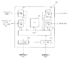
図1は、本実施の形態に係る画像処理装置のシステム構成を示すブロック図である。同図において、1はリーダ部で、原稿の画像を読み取り、原稿画像に応じた画像データを後述する画像入出力制御部3へ出力する。2はプリンタ部で、画像入出力制御部3からの画像データに応じた画像を記録紙上に記録する。3は画像入出力制御部で、リーダ部1及びプリンタ部2に接続されており、ファクシミリ部4、ネットワーク・インターフェース部5、コンピュータ・インターフェース部6及びコア部10等からなる。
【0015】
ファクシミリ部4は電話回線11を介して受信した圧縮画像データを伸長して、該伸長された画像データをコア部10へ転送し、また、このコア部10から転送された画像データを圧縮して、該圧縮された画像データを電話回線11を介して送信するものである。
【0016】
ネットワーク・インターフェース部5はローカルエリアネットワークまたはワイドエリアネットワーク(LAN/WAN)12とコア部10との間のインターフェースである。
【0017】
コンピュータ・インターフェース部6はパーソナルコンピュータまたはワークステーション(PC/WS)13とコア部10との間のインターフェースである。
【0018】
コア部10はリーダ部1、プリンタ部2、ファクシミリ部4、ネットワーク・インターフェース5、コンピュータ・インターフェース部6のそれぞれの間のデータの流れを制御するものである。
【0019】
図2は、リーダ部1及びプリンタ部2の構成を示す縦断面図である。同図において、リーダ部1の原稿給送装置101は原稿を最終頁から順に1枚ずつプラテンガラス102上へ給送し、原稿の読み取り動作終了後、プラテンガラス102上の原稿を排出するものである。
【0020】
原稿がプラテンガラス102上に搬送されると、ランプ103を点灯し、スキャナユニット104の移動を開始させて、原稿を露光走査する。このときの原稿からの反射光は、ミラー105,106,107及びレンズ108によってCCDイメージセンサ(以下、CCDと記述する)109へ導かれる。このように走査された原稿の画像は、CCD109によって読み取られる。CCD109から出力される画像データは、所定の処理が施された後、画像入出力制御部3のコア部10へ転送される。
【0021】
プリンタ部2のレーザードライバー201はレーザー発光部201aを駆動するものであり、コア部10から出力された画像データに応じたレーザー光をレーザー発光部201aに発光させる。このレーザー光は感光ドラム202に照射され、該感光ドラム202にはレーザー光に応じた潜像が形成される。この感光ドラム202の潜像の部分には現像器203によって現像剤が付着される。そして、レーザー光の照射開始と同期したタイミングで、上段給紙カセット204及び下段給紙カセット205のいずれかから記録紙を給紙して転写部206へ搬送し、感光ドラム202に付着された現像剤を記録紙に転写する。現像剤が転写された記録紙は定着部207へ搬送され、該定着部207の熱と圧力により現像剤は記録紙に定着される。定着部207を通過した記録紙は排出ローラ208によって排出され、ソータ211は排出された記録紙をそれぞれのビン212に収納して記録紙の仕分けを行う。
【0022】
尚、ソータ211は仕分けが設定されていない場合は最上部のビン212に記録紙を収納する。また、両面記録が設定されている場合は、排出ローラ208のところまで記録紙を搬送した後、排出ローラ208の回転方向を逆転させ、フラッパ209によって再給紙搬走路210へ導く。また、多重記録が設定されている場合は、記録紙を排出ローラ208まで搬送しないようにフラッパ209によって再給紙搬走路210へ導く。再給紙搬走路210へ導かれた記録紙は、上述したタイミングで転写部206へ搬送される。
【0023】
図3は、リーダ部1の内部構成を示すブロック図である。同図において、109はCCD、110はA/D変換・シェーディング補正部(以下、A/D・SH部と記述する)、111は画像処理部、112はインターフェース(I/F)、113はCPU(中央処理装置)、114は操作部、115はメモリである。
【0024】
図3において、CCD109から出力された画像データは、A/D・SH部110でアナログ/デジタル変換処理が行われると共に、シェーディング補正処理が行われる。A/D・SH部110によって処理された画像データは、画像処理部111、インターフェース(I/F)112を介して画像入出力制御部3のコア部10へ転送される。
【0025】
CPU(中央処理装置)113は操作部114で設定された設定内容に応じて画像処理部111及びインターフェース112を制御する。例えば、操作部114でトリミング処理を行って複写を行う複写モードが設定されている場合は、画像処理部111でトリミング処理を行わせて、インターフェース112から画像データと設定されたモードに応じた制御コマンドをコア部10へ転送させる。また、操作部114でファクシミリ送信モードが設定されている場合は、インターフェース112から画像データと設定されたモードに応じた制御コマンドをコア部10へ転送させる。
【0026】
このようなCPU113の制御プログラムはメモリ115に格納されており、CPU113はメモリ115内の制御プログラムを参照しながら制御を行う。また、メモリ115はCPU113の作業領域としても使われる。
【0027】
図4は、コア部10の内部構成を示すブロック図である。同図において、121は制御LSI、122はメモリ、123はハードディスクドライブ(HDD)、124、125および126は画像処理LSIである。制御LSI121は、CPU、メモリコントローラ、HDDコントローラ、外部I/F等を内部に持つ高集積度LSIであり、メモリ122に格納されたプログラムによって画像処理LSIの動作および画像データの流れを制御する。メモリ122は、制御LSI121のプログラムを格納するとともに、制御LSI121の作業領域として使用される。HDD123は、制御LSI121のプログラムを格納するとともに、画像データの一時記憶として使用される。画像処理LSI124、125、126は、複数の画像処理手段および画像入出力装置I/Fを内部に持つ高集積度LSIであり、制御LSI121の制御によって画像処理動作および画像入出力動作をするものである。
【0028】
図4において、リーダ部1からの画像データは画像処理LSI126へ転送されると共に、リーダ部1からの制御コマンドは画像処理LSI126を介して制御LSI121へ転送される。リーダ部1から画像処理LSI126へ転送された画像データは、HDD123に格納される。
【0029】
電話回線11からファクシミリ部4に対して入力された画像を表すコードデータは、ファクシミリ部4において画像データに展開される。該展開された画像データは、制御LSI121へ転送され、HDD123に格納される。
【0030】
LAN/WAN12からネットワーク・インターフェース部5に対して入力された画像データは、ネットワーク・インターフェース部5を介して制御LSI121へ転送され、HDD123に格納される。
【0031】
また、PC/WS13からコンピュータ・インターフェース部6に対して入力された画像を表わすコードデータは、コンピュータ・インターフェース部6において画像データに展開される。該展開された画像データは画像処理LSI125および画像処理LSI126を介して制御LSI121へ転送され、HDD123に格納される。
【0032】
リーダ部1、ファクシミリ部4、ネットワーク・インターフェース部5またはコンピュータ・インターフェース部6から画像データとともに転送された制御コマンドに応じて、HDD123に一時格納された画像データは制御LSI121を介してファクシミリ部4、ネットワーク・インターフェース部5または画像処理LSI124を介してプリンタ部2へ転送される。
【0033】
制御LSI121は、メモリ122に記憶されている制御プログラム及びリーダ部1から転送された制御コマンドおよび画像データとともに転送された制御コマンドに従って上述したような制御を行う。このように、コア部10を中心に原稿画像の読み取り、画像のプリント、画像の送受信、PC/WS13からのデータの入出力等の機能を複合させた処理を行うことが可能である。
【0034】
図5は、画像処理LSI126の内部構成を示すブロック図である。同図において、130は変倍処理部、131は回転・反転処理部、132は色変換処理部、133は圧縮・伸張処理部、134は外部画像I/F部、135はデータ入力部、136はデータ出力部、137は接続切換部である。
【0035】
図6は、画像処理LSI125の内部構成を示すブロック図である。同図において、140は変倍処理部、141は回転・反転処理部、142は色変換処理部、143は圧縮・伸張処理部、144は外部画像I/F部、145はデータ入力部、146はデータ出力部、147は接続切換部である。この画像処理LSI125には、前述の画像処理LSI126と同じ高集積度LSIを用いている。
【0036】
図7は、画像処理LSI124の内部構成を示すブロック図である。同図において、150は変倍処理部、151は回転・反転処理部、152は色変換処理部、153は圧縮・伸張処理部、154は外部画像I/F部、155はデータ入力部、156はデータ出力部、157は接続切換部である。この画像処理LSI124には、前述の画像処理LSI126および125と同じ高集積度LSIを用いている。
【0037】
図8は、画像処理LSI124内部の接続切替部137の内部構成を示すブロック図である。同図において、160、161、162、163、164および165はセレクタである。これらのセレクタは、画像データが入力されるよりも前にあらかじめ入力される制御コマンドによって制御され、各画像データ転送元からの画像データが、いずれかのセレクタから出力されるように画像データの出力先を切り換える動作を行うものである。各セレクタは独立に制御可能で、複数の入力元から入力される複数の画像データを、それぞれ別の出力先に同時に出力することが可能である。例えば、外部画像I/F部134から入力される画像データをセレクタ160から出力しながら、データ入力部135から入力される画像データをセレクタ161から出力するといった、複数の入力画像を同時に別々の出力先に出力することが可能である。なお、画像処理LSI125および126内部の接続切替部147および157の内部構成を示すブロック図は、接続切替部137の内部構成を示すブロック図と同様のものであるため省略する。
【0038】
図9は、画像データを、コア部10内部(すなわち制御LSI121、画像処理LSI124、同125および同126の間、および、各画像処理LSI内部の各処理部の間)において転送するときの、タイミングチャートである。データ転送時には、データ送信側のLSIまたは処理部はまず転送開始信号を1クロック幅の間アクティブにし、それに続けて属性データを4クロック幅の間送信する。そして属性データに続けて画像データを送信する。データ受信側のLSIまたは処理部は、この規則に合わせてクロック信号に同期してデータを受信する。なお、この属性データには、画像データ転送時の画像データ長が含まれ、画像データ転送制御に使用される。また、転送先のLSIの順序を示す「チップIDリスト」、画像処理の順序を示す「処理IDリスト」、また、画像データがカラーか白黒か、圧縮されているか、といった画像処理部で使用される画像の属性情報が含まれる。
【0039】
属性データは、コア部10内部での各LSI間および各画像処理LSI内部の各処理部間での画像データ転送時に常に画像データに付加されて転送されるものである。各LSIおよび各画像処理LSI内部の各処理部では受信した属性データを保持し、画像データを送信する際に保持しておいた属性データを画像データに付加して送信するという構成となっている。ただし、後述するように、属性データを送信するときに一部の属性を書き換える場合もある。また、リーダ部1、コンピュータ・インターフェース部6、ファクシミリ部4およびネットワーク・インターフェース部5から画像が入力された時点には画像データに属性データは付加されていないため、画像データに属性データを付加する作業が行われる。具体的には、画像データを受信した各LSIまたは各処理部は制御LSI121によってあらかじめ設定されていた属性データをその画像データの属性データとして付加し、送信するという構成となっている。さらに、プリンタ部2、ファクシミリ部4およびネットワーク・インターフェース部5へ画像データを転送するときには、属性データは切り捨てられて、画像データのみが送信される。
【0040】
図10は、制御LSI121の内部構成を示すブロック図である。同図において、170はCPU、171はファクシミリI/F部、172はネットワークI/F部、173はメモリコントローラ部、174はHDDコントローラ部、175はデータ入力部、176はデータ出力部、177は内部バスである。
【0041】
画像処理LSI126の動作を以下に説明する。
【0042】
図5において、リーダ部1からの画像データは、外部画像I/F部134に入力される。外部画像I/F部134は画像データに属性データを付加して接続切換部137へ転送する。なお、この付加する属性データ値は、前述の通り、あらかじめ制御LSI121によって外部画像I/F部134に設定しておいた値である。
【0043】
画像データが接続切換部137へ転送されると、接続切換部137は属性データの処理IDリストの先頭のID番号を読み取った後、それを処理IDリストから削除して2番目のID番号が先頭になるように属性データを変更する。そして、元の先頭のID番号が0の場合には変倍処理部130へ、1の場合には回転・反転処理部131へ、2の場合には色変換処理部132へ、3の場合には圧縮・伸張処理部133へ、4の場合には外部画像I/F部134へ、あるいは5の場合にはデータ出力部136へ、画像データを属性データと共に転送する。このときの接続切換部137の動作は、ID番号によって内部セレクタの出力を切り換えるという動作となる。そして、接続切換部137から各画像処理部、つまり、変倍処理部130、回転・反転処理部131、色変換処理部132または圧縮・伸張処理部133、に転送された画像データは、各画像処理部において画像処理が施された後に再度接続切換部137に転送される。以上の動作を画像データがデータ出力部136に転送されるまで繰り返し処理する。この繰り返しにより、画像データはあらかじめ設定された任意の数の画像処理が連続的に施されることになる。なお、本実施の形態における画像処理LSI126では、外部画像I/F部134は画像データ出力部としては機能させない構成としているため、外部画像I/F部134に画像データが出力されないようにあらかじめ属性データの処理IDリストを設定しておく。具体的には、ID番号4は設定しないように制御LSI121で制御する。
【0044】
そして最後に、データ出力部136に転送された画像データは、制御LSI121へ転送される。
【0045】
また、図5において、画像処理LSI125から入力された画像データは、データ入力部135に入力される。データ入力部135は、まず画像データの持つ属性データのチップIDリストの先頭のID番号を読み取る。そして、先頭のID番号と、制御LSI121によってあらかじめデータ入力部135に設定してあるID番号とを比較し、異なる値であれば画像データをデータ出力部136へ転送し、データ出力部136は画像データを制御LSI121へ転送する。また、比較した結果、同じ値であれば、データ入力部135は、チップIDリストの先頭のID番号をチップIDリストから削除して2番目のID番号が先頭になるように属性データを変更する。そして、画像データを接続切換部137へ転送し、前述の外部画像I/F134から接続切換部137へ転送された場合と同様に、画像データは処理IDリストにあらかじめ設定された順番に画像処理部で画像処理が施されてからデータ出力部136へ転送される。データ出力部136へ転送された画像データは、制御LSI121へ転送される。
【0046】
画像処理LSI125の動作を以下に説明する。なお、画像処理LSI125は、画像処理LSI126と同じLSIを使用しているため、内部動作は同じである。ただし、画像データの入力元および出力先が異なるため、データの入出力が異なる。
【0047】
図6において、コンピュータ・インターフェース部6からの画像データは、外部画像I/F部144に入力される。外部画像I/F部144は画像データに属性データを付加して接続切換部147へ転送する。なお、この付加する属性データ値は、前述の通り、あらかじめ制御LSI121によって外部画像I/F部144に設定しておいた値である。
【0048】
画像データが接続切換部147へ転送されると、接続切換部147は属性データの処理IDリストの先頭のID番号を読み取った後、それを処理IDリストから削除して2番目のID番号が先頭になるように属性データを変更する。そして、元の先頭のID番号が0の場合には変倍処理部140へ、1の場合には回転・反転処理部141へ、2の場合には色変換処理部142へ、3の場合には圧縮・伸張処理部143へ、4の場合には外部画像I/F部144へ、あるいは5の場合にはデータ出力部146へ、画像データを属性データと共に転送する。このときの接続切換部147の動作は、ID番号によって内部セレクタの出力を切り換えるという動作となる。そして、接続切換部147から各画像処理部、つまり、変倍処理部140、回転・反転処理部141、色変換処理部142または圧縮・伸張処理部143、に転送された画像データは、各画像処理部において画像処理が施された後に再度接続切換部147に転送される。以上の動作を画像データがデータ出力部146に転送されるまで繰り返し処理する。この繰り返しにより、画像データはあらかじめ設定された任意の数の画像処理が連続的に施されることになる。なお、本実施の形態における画像処理LSI125では、外部画像I/F部144は画像データ出力部としては機能させない構成としているため、外部画像I/F部144に画像データが出力されないようにあらかじめ属性データの処理IDリストを設定しておく。具体的には、ID番号4は設定しないように制御LSI121で制御する。
【0049】
そして最後に、データ出力部146に転送された画像データは、画像処理LSI126へ転送される。
【0050】
また、図6において、画像処理LSI124から入力された画像データは、データ入力部145に入力される。データ入力部145は、まず画像データの持つ属性データのチップIDリストの先頭のID番号を読み取る。そして、先頭のID番号と、制御LSI121によってあらかじめデータ入力部145に設定してあるID番号とを比較し、異なる値であれば画像データをデータ出力部146へ転送し、データ出力部146は画像データを制御LSI121へ転送する。また、比較した結果、同じ値であれば、データ入力部145は、チップIDリストの先頭のID番号をチップIDリストから削除して2番目のID番号が先頭になるように属性データを変更する。そして、画像データを接続切換部147へ転送し、前述の外部画像I/F144から接続切換部147へ転送された場合と同様に、画像データは処理IDリストにあらかじめ設定された順番に画像処理部で画像処理が施されてからデータ出力部146へ転送される。データ出力部146へ転送された画像データは、画像処理LSI126へ転送される。
【0051】
画像処理LSI124の動作を以下に説明する。なお、画像処理LSI124は、画像処理LSI126および画像処理LSI125と同じLSIを使用しているため、内部動作は同じである。ただし、画像データの入力元および出力先が異なるため、データの入出力が異なる。
【0052】
図7において、制御LSI121から入力された画像データは、データ入力部155に入力される。データ入力部155は、まず画像データの持つ属性データのチップIDリストの先頭のID番号を読み取る。そして、先頭のID番号と、制御LSI121によってあらかじめデータ入力部155に設定してあるID番号とを比較し、異なる値であれば画像データをデータ出力部156へ転送し、データ出力部156は画像データを制御LSI121へ転送する。また、比較した結果、同じ値であれば、データ入力部155は、チップIDリストの先頭のID番号をチップIDリストから削除して2番目のID番号が先頭になるように属性データを変更する。そして、画像データが接続切換部157へ転送されると、接続切換部157は属性データの処理IDリストの先頭のID番号を読み取った後、それを処理IDリストから削除して2番目のID番号が先頭になるように属性データを変更する。そして、元の先頭のID番号が0の場合には変倍処理部150へ、1の場合には回転・反転処理部151へ、2の場合には色変換処理部152へ、3の場合には圧縮・伸張処理部153へ、4の場合には外部画像I/F部154へ、あるいは5の場合にはデータ出力部156へ、画像データを属性データと共に転送する。このときの接続切換部157の動作は、ID番号によって内部セレクタの出力を切り換えるという動作となる。そして、接続切換部157から各画像処理部、つまり、変倍処理部150、回転・反転処理部151、色変換処理部152または圧縮・伸張処理部153、に転送された画像データは、各画像処理部において画像処理が施された後に再度接続切換部157に転送される。以上の動作を画像データがデータ出力部156または外部画像I/F部154へ転送されるまで繰り返し処理する。この繰り返しにより、画像データはあらかじめ設定された任意の数の画像処理が連続的に施されることになる。そして、画像データがデータ出力部156へ転送された場合、画像データは画像処理LSI125へ転送される。また、画像データが外部画像I/F部154へ転送された場合、画像データはプリンタ部2へ転送され、プリンタ部2で印刷出力される。
【0053】
制御LSI121の動作を以下に説明する。
【0054】
図10において、ファクシミリ部4からの画像データは、ファクシミリI/F部171に入力される。ファクシミリI/F部171は、CPU170の制御により、受信した画像データをHDDコントローラ174を介してHDD123へ格納する。ネットワーク・インターフェース部5からの画像データは、ネットワークI/F部172に入力される。ネットワークI/F部172は、CPU170の制御により、受信した画像データをHDDコントローラ174を介してHDD123へ格納する。
【0055】
また、図10において、画像処理LSI126から入力された画像データは、データ入力部175に入力される。データ入力部175は、まず画像データの持つ属性データのチップIDリストの先頭のID番号を読み取る。そして、先頭のID番号と、CPU170によってあらかじめデータ入力部175に設定してあるID番号とを比較し、異なる値であれば画像データをデータ出力部176へ転送し、データ出力部176は画像データを画像処理LSI124へ転送する。また、比較した結果、同じ値であれば、データ入力部175は、チップIDリストの先頭のID番号をチップIDリストから削除して2番目のID番号が先頭になるように属性データを変更する。そして、画像データを内部バス177およびHDDコントローラ部174を介してHDD123へ転送する。
【0056】
さらに、図10において、CPU170の制御によりHDD123から読み出された画像データは、HDDコントローラ部174および内部バス177を介してデータ出力部176、ファクシミリI/F部171またはネットワークI/F部172へ転送される。なお、ここでの転送先は、ファクシミリI/F部171、ネットワークI/F部172およびデータ入力部175を介してCPU170が受信した画像データ出力要求に応じて決定され、CPU170により内部バス177が制御されて切り換えられる。画像データがファクシミリI/F部171へ転送された場合は、ファクシミリI/F部171は画像データをファクシミリ部4へ転送してファクシミリ送信を行う。画像データがネットワークI/F部172へ転送された場合は、ネットワークI/F部172は画像データをネットワーク・インターフェース部5へ転送する。画像データがデータ出力部176へ転送された場合は、データ出力部176は画像データに属性データを付加して画像処理LSI124へ転送する。なお、この付加する属性データ値は、あらかじめCPU170によってデータ出力部176に設定しておいた値である。
【0057】
以上のような構成で、コア部10の画像データの流れを例を挙げて説明する。
【0058】
リーダ部1で読み取った原稿の画像データを、ファクシミリ部4で電話回線11に対して送信し、かつ、同時にプリンタ部2でプリント出力する動作を例にする。
【0059】
まず、操作者は、原稿を原稿給送装置101に載せ、操作部114を操作してファクシミリ送信とプリントを同時に行うモードにする。そして、操作部114でファクシミリ送信プリントモードが設定された場合は、CPU113はインターフェース112を介して設定されたモードに応じた制御コマンドをコア部10に対して送信する。ファクシミリ送信プリントモードの制御コマンドは画像処理LSI126を介して制御LSI121内部のCPU170に転送される。
【0060】
CPU170は、各処理部をファクシミリ送信プリントモードに設定するための制御コマンドを制御LSI121内部の各処理部および各画像処理LSIへ転送する。具体的には、外部画像I/F部134には、属性データの初期値として、チップIDリストを{0}に、処理IDリストを{3,5}と設定する。また、各LSIのデータ入力部にチップIDを次のように設定する。制御LSI121内部のデータ入力部175には0を、画像処理LSI126内部のデータ入力部135には3を、画像処理LSI125内部のデータ入力部145には2を、画像処理LSI124内部のデータ入力部155には1を設定する。それから、制御LSI121内部のデータ出力部176に属性データの初期値を、プリント出力する画像データ用、および、ファクシミリ送信する画像データ用とを別々に設定する。つまり、プリント出力する画像データ用の初期値としてチップIDリストを{1}に、処理IDリストを{3,0,2,4}にし、また、ファクシミリ送信用する画像データ用の初期値としてチップIDリストを{2,0}に、処理IDリストを{3,0,1,2,5}に設定する。
【0061】
そして、リーダ部1からコア部10へ画像データが転送開始されて、外部画像I/F部134に入力された画像データは、外部画像I/F部134によって属性データが付加され、接続切換部137へ転送される。このとき付加される属性データは、チップIDリストが{0}で、処理IDリストが{3,5}である。接続切換部137では、この処理IDリスト{3,5}の先頭のID番号3を読み取って、画像データをID番号3に対応する圧縮・伸張処理部133に転送する。それと同時に処理IDリストの先頭のID番号3を削除した{5}を新しい処理IDリストとする。圧縮・伸張処理部133では、画像データを圧縮処理して再度接続切換部137へ転送する。接続切換部137では、処理IDリスト{5}の先頭のID番号5を読み取って、画像データをID番号5に対応するデータ出力部136に転送する。それと同時に処理IDリスト{5}の先頭のID番号5を削除した{}(空リスト)を新しい処理IDリストとする。データ出力部136は、画像データを制御LSI121へ転送する。制御LSI121内部のデータ入力部175は、画像データの属性データのチップIDリスト{0}の先頭のチップID番号0を読み取って、データ入力部175にあらかじめ設定してあるチップID番号0と比較する。比較の結果、値が同じであるので、画像データを内部バス177およびHDDコントローラ174を介してHDD123へ格納する。
【0062】
HDD123に画像データが格納されると、CPU170の制御により、この画像データをファクシミリ部4およびプリンタ部2へ転送する動作が開始される。
【0063】
ファクシミリ部4へ転送される画像データは、まず、HDD123から読み出され、HDDコントローラ部174および内部バス177を介してデータ出力部176に転送される。データ出力部176に転送された画像データは、データ出力部176によって属性データが付加され、画像処理LSI124へ転送される。このとき付加される属性データは、チップIDリストが{2,0}で、処理IDリストが{3,0,1,2,5}である。画像処理LSI124内部のデータ入力部155は、画像データの属性データのチップIDリスト{2,0}の先頭のチップID番号2を読み取って、データ入力部155にあらかじめ設定してあるチップID番号1と比較する。比較の結果、値が異なるので、画像データをデータ出力部156へ転送する。データ出力部156は、画像データを画像処理LSI125へ転送する。画像処理LSI125内部のデータ入力部145は、画像データの属性データのチップIDリスト{2,0}の先頭のチップID番号2を読み取って、データ入力部145にあらかじめ設定してあるチップID番号2と比較する。比較の結果、値が同じであるので、画像データを接続切換部147へ転送する。それと同時にチップIDリスト{2,0}の先頭のチップID番号2を削除した{0}を新しいチップIDリストとする。接続切換部147は処理IDリスト{3,0,1,2,5}の先頭のID番号3を読み取って、画像データをID番号3に対応する圧縮・伸張処理部143に転送する。それと同時に処理IDリストの先頭のID番号3を削除した{0,1,2,5}を新しい処理IDリストとする。圧縮・伸張処理部143では、画像データを伸張処理して再度接続切換部147へ転送する。接続切換部147では、処理IDリスト{0,1,2,5}の先頭のID番号0を読み取って、画像データをID番号0に対応する変倍処理部140へ転送する。それと同時に処理IDリスト{0,1,2,5}の先頭のID番号0を削除した{1,2,5}を新しい処理IDリストとする。変倍処理部140では、画像データを変倍処理して再度接続切換部147へ転送する。接続切換部147では、処理IDリスト{1,2,5}の先頭のID番号1を読み取って、画像データをID番号1に対応する回転・反転処理部141へ転送する。それと同時に処理IDリスト{1,2,5}の先頭のID番号1を削除した{2,5}を新しい処理IDリストとする。回転・反転処理部141では、画像データを回転処理して再度接続切換部147へ転送する。接続切換部147では、処理IDリスト{2,5}の先頭のID番号2を読み取って、画像データをID番号2に対応する色変換処理部142へ転送する。それと同時に処理IDリスト{2,5}の先頭のID番号2を削除した{5}を新しい処理IDリストとする。色変換処理部142では、画像データを色変換して再度接続切換部147へ転送する。接続切換部147では、処理IDリスト{5}の先頭のID番号5を読み取って、画像データをID番号5に対応するデータ出力部146に転送する。それと同時に処理IDリスト{5}の先頭のID番号5を削除した{}(空リスト)を新しい処理IDリストとする。データ出力部146は、画像データを制御LSI121へ転送する。制御LSI121内部のデータ入力部175は、画像データの属性データのチップIDリスト{0}の先頭のチップID番号0を読み取って、データ入力部175にあらかじめ設定してあるチップID番号0と比較する。比較の結果、値が同じであるので、画像データを内部バス177およびファクシミリI/F部171を介してファクシミリ部4へ転送し、ファクシミリ部4は電話回線11へ画像データを送信する。
【0064】
プリンタ部2へ転送される画像データは、まず、HDD123から読み出され、HDDコントローラ部174および内部バス177を介してデータ出力部176に転送される。データ出力部176に転送された画像データは、データ出力部176によって属性データが付加され、画像処理LSI124へ転送される。このとき付加される属性データは、チップIDリストが{1}で、処理IDリストが{3,0,2,4}である。画像処理LSI124内部のデータ入力部155は、画像データの属性データのチップIDリスト{1}の先頭のチップID番号1を読み取って、データ入力部155にあらかじめ設定してあるチップID番号1と比較する。比較の結果、値が同じであるので、画像データを接続切換部157へ転送する。それと同時にチップIDリスト{1}の先頭のチップID番号1を削除した{}(空リスト)を新しいチップIDリストとする。接続切換部157は処理IDリスト{3,0,2,4}の先頭のID番号3を読み取って、画像データをID番号3に対応する圧縮・伸張処理部153に転送する。それと同時に処理IDリストの先頭のID番号3を削除した{0,2,4}を新しい処理IDリストとする。圧縮・伸張処理部153では、画像データを伸張処理して再度接続切換部157へ転送する。接続切換部157では、処理IDリスト{0,2,4}の先頭のID番号0を読み取って、画像データをID番号0に対応する変倍処理部150へ転送する。それと同時に処理IDリスト{0,2,4}の先頭のID番号0を削除した{2,4}を新しい処理IDリストとする。変倍処理部150では、画像データを変倍処理して再度接続切換部157へ転送する。接続切換部157では、処理IDリスト{2,4}の先頭のID番号2を読み取って、画像データをID番号2に対応する色変換処理部152へ転送する。それと同時に処理IDリスト{2,4}の先頭のID番号2を削除した{4}を新しい処理IDリストとする。色変換処理部152では、画像データを色変換して再度接続切換部157へ転送する。接続切換部157では、処理IDリスト{4}の先頭のID番号4を読み取って、画像データをID番号4に対応する外部画像I/F部154に転送する。それと同時に処理IDリスト{4}の先頭のID番号4を削除した{}(空リスト)を新しい処理IDリストとする。外部画像I/F部154は、画像データをプリンタ部2へ転送し、プリンタ部は画像データをプリント出力する。
【0065】
ここまで述べたように、リーダ部2で一度読み取った画像データを、ファクシミリ送信に適した解像度に変倍処理し、出力の方向を回転して合わせ、色空間を補正して送信することと、プリント出力に適した解像度に変倍処理し、色空間を補正してプリント出力することが実現できる。
【0066】
[実施の形態2]
以下、本発明の一実施の形態を図面に基づき説明する。
【0067】
図11は、本実施の形態に係る画像処理装置のシステム構成を示すブロック図である。同図において、2はプリンタ部で、画像入出力制御部3からの画像データに応じた画像を記録紙上に記録する。3は画像入出力制御部で、プリンタ部2に接続されており、コンピュータ・インターフェース部6及びコア部10等からなる。
【0068】
コンピュータ・インターフェース部6はパーソナルコンピュータまたはワークステーション(PC/WS)13とコア部10との間のインターフェースである。
【0069】
コア部10はプリンタ部2、コンピュータ・インターフェース部6の間のデータの流れを制御するものである。
【0070】
図12は、プリンタ部2の構成を示す縦断面図である。同図において、プリンタ部2のレーザードライバー201はレーザー発光部201aを駆動するものであり、コア部10から出力された画像データに応じたレーザー光をレーザー発光部201aに発光させる。このレーザー光は感光ドラム202に照射され、該感光ドラム202にはレーザー光に応じた潜像が形成される。この感光ドラム202の潜像の部分には現像器203によって現像剤が付着される。そして、レーザー光の照射開始と同期したタイミングで、上段給紙カセット204及び下段給紙カセット205のいずれかから記録紙を給紙して転写部206へ搬送し、感光ドラム202に付着された現像剤を記録紙に転写する。現像剤が転写された記録紙は定着部207へ搬送され、該定着部207の熱と圧力により現像剤は記録紙に定着される。定着部207を通過した記録紙は排出ローラ208によって排出され、ソータ211は排出された記録紙をそれぞれのビン212に収納して記録紙の仕分けを行う。
【0071】
尚、ソータ211は仕分けが設定されていない場合は最上部のビン212に記録紙を収納する。また、両面記録が設定されている場合は、排出ローラ208のところまで記録紙を搬送した後、排出ローラ208の回転方向を逆転させ、フラッパ209によって再給紙搬走路210へ導く。また、多重記録が設定されている場合は、記録紙を排出ローラ208まで搬送しないようにフラッパ209によって再給紙搬走路210へ導く。再給紙搬走路210へ導かれた記録紙は、上述したタイミングで転写部206へ搬送される。
【0072】
図13は、コア部10の内部構成を示すブロック図である。同図において、121は制御LSI、122はメモリ、123はハードディスクドライブ(HDD)、124および125は画像処理LSIである。制御LSI121は、CPU、メモリコントローラ、HDDコントローラ、外部I/F等を内部に持つ高集積度LSIであり、メモリ122に格納されたプログラムによって画像処理LSIの動作および画像データの流れを制御する。メモリ122は、制御LSI121のプログラムを格納するとともに、制御LSI121の作業領域として使用される。HDD123は、制御LSI121のプログラムを格納するとともに、画像データの一時記憶として使用される。画像処理LSI124、125は、複数の画像処理手段および画像入出力装置I/Fを内部に持つ高集積度LSIであり、制御LSI121の制御によって画像処理動作および画像入出力動作をするものである。
【0073】
図13において、PC/WS13からコンピュータ・インターフェース部6に対して入力された画像を表わすコードデータは、コンピュータ・インターフェース部6において画像データに展開される。該展開された画像データは画像処理LSI125を介して制御LSI121へ転送され、HDD123に格納される。
【0074】
コンピュータ・インターフェース部6から画像データとともに転送された制御コマンドに応じて、HDD123に一時格納された画像データは制御LSI121および画像処理LSI124を介してプリンタ部2へ転送される。
【0075】
制御LSI121は、メモリ122に記憶されている制御プログラム及びリーダ部1から転送された制御コマンドおよび画像データとともに転送された制御コマンドに従って上述したような制御を行う。このように、コア部10を中心に画像のプリント、PC/WS13からのデータの入力等の処理を行うことが可能である。
【0076】
図14は、画像処理LSI125の内部構成を示すブロック図である。同図において、140は変倍処理部、141は回転・反転処理部、142は色変換処理部、143は圧縮・伸張処理部、144は外部画像I/F部、145はデータ入力部、146はデータ出力部、147は接続切換部である。
【0077】
図15は、画像処理LSI124の内部構成を示すブロック図である。同図において、150は変倍処理部、151は回転・反転処理部、152は色変換処理部、153は圧縮・伸張処理部、154は外部画像I/F部、155はデータ入力部、156はデータ出力部、157は接続切換部である。この画像処理LSI124には、前述の画像処理LSI125と同じ高集積度LSIを用いている。
【0078】
画像処理LSI125内部の接続切替部147および画像処理LSI124内部の接続切替部157の内部構成を示すブロック図は、実施の形態1における画像処理LSI126内部の接続切換部137の内部構成を示すブロック図と同様のものであるため省略する。
【0079】
図9は、画像データを、コア部10内部(すなわち制御LSI121、画像処理LSI124および同125の間、および、各画像処理LSI内部の各処理部の間)において転送するときの、タイミングチャートである。データ転送時には、データ送信側のLSIまたは処理部はまず転送開始信号を1クロック幅の間アクティブにし、それに続けて属性データを4クロック幅の間送信する。そして属性データに続けて画像データを送信する。データ受信側のLSIまたは処理部は、この規則に合わせてクロック信号に同期してデータを受信する。なお、この属性データには、画像データ転送時の画像データ長が含まれ、画像データ転送制御に使用される。また、転送先のLSIの順序を示す「チップIDリスト」、画像処理の順序を示す「処理IDリスト」、また、画像データがカラーか白黒か、圧縮されているか、といった画像処理部で使用される画像の属性情報が含まれる。
【0080】
属性データは、コア部10内部での各LSI間および各画像処理LSI内部の各処理部間での画像データ転送時に常に画像データに付加されて転送されるものである。各LSIおよび各画像処理LSI内部の各処理部では受信した属性データを保持し、画像データを送信する際に保持しておいた属性データを画像データに付加して送信するという構成となっている。ただし、後述するように、属性データを送信するときに一部の属性を書き換える場合もある。また、コンピュータ・インターフェース部6から画像が入力された時点には画像データに属性データは付加されていないため、画像データに属性データを付加する作業が行われる。具体的には、画像データを受信した各LSIまたは各処理部は制御LSI121によってあらかじめ設定されていた属性データをその画像データの属性データとして付加し、送信するという構成となっている。さらに、プリンタ部2へ画像データを転送するときには、属性データは切り捨てられて、画像データのみが送信される。
【0081】
図16は、制御LSI121の内部構成を示すブロック図である。同図において、170はCPU、171はファクシミリI/F部、172はネットワークI/F部、173はメモリコントローラ部、174はHDDコントローラ部、175はデータ入力部、176はデータ出力部、177は内部バスである。
【0082】
画像処理LSI125の動作を以下に説明する。
【0083】
図14において、コンピュータ・インターフェース部6からの画像データは、外部画像I/F部144に入力される。外部画像I/F部144は画像データに属性データを付加して接続切換部147へ転送する。なお、この付加する属性データ値は、前述の通り、あらかじめ制御LSI121によって外部画像I/F部144に設定しておいた値である。
【0084】
画像データが接続切換部147へ転送されると、接続切換部147は属性データの処理IDリストの先頭のID番号を読み取った後、それを処理IDリストから削除して2番目のID番号が先頭になるように属性データを変更する。そして、元の先頭のID番号が0の場合には変倍処理部140へ、1の場合には回転・反転処理部141へ、2の場合には色変換処理部142へ、3の場合には圧縮・伸張処理部143へ、4の場合には外部画像I/F部144へ、あるいは5の場合にはデータ出力部146へ、画像データを属性データと共に転送する。このときの接続切換部147の動作は、ID番号によって内部セレクタの出力を切り換えるという動作となる。そして、接続切換部147から各画像処理部、つまり、変倍処理部140、回転・反転処理部141、色変換処理部142または圧縮・伸張処理部143、に転送された画像データは、各画像処理部において画像処理が施された後に再度接続切換部147に転送される。以上の動作を画像データがデータ出力部146に転送されるまで繰り返し処理する。この繰り返しにより、画像データはあらかじめ設定された任意の数の画像処理が連続的に施されることになる。なお、本実施の形態における画像処理LSI125では、外部画像I/F部144は画像データ出力部としては機能させない構成としているため、外部画像I/F部144に画像データが出力されないようにあらかじめ属性データの処理IDリストを設定しておく。具体的には、ID番号4は設定しないように制御LSI121で制御する。
【0085】
そして最後に、データ出力部146に転送された画像データは、制御LSI121へ転送される。
【0086】
また、図14において、画像処理LSI124から入力された画像データは、データ入力部145に入力される。データ入力部145は、まず画像データの持つ属性データのチップIDリストの先頭のID番号を読み取る。そして、先頭のID番号と、制御LSI121によってあらかじめデータ入力部145に設定してあるID番号とを比較し、異なる値であれば画像データをデータ出力部146へ転送し、データ出力部146は画像データを制御LSI121へ転送する。また、比較した結果、同じ値であれば、データ入力部145は、チップIDリストの先頭のID番号をチップIDリストから削除して2番目のID番号が先頭になるように属性データを変更する。そして、画像データを接続切換部147へ転送し、前述の外部画像I/F144から接続切換部147へ転送された場合と同様に、画像データは処理IDリストにあらかじめ設定された順番に画像処理部で画像処理が施されてからデータ出力部146へ転送される。データ出力部146へ転送された画像データは、制御LSI121へ転送される。
【0087】
画像処理LSI124の動作を以下に説明する。なお、画像処理LSI124は、画像処理LSI125と同じLSIを使用しているため、内部動作は同じである。ただし、画像データの入力元および出力先が異なるため、データの入出力が異なる。
【0088】
図15において、制御LSI121から入力された画像データは、データ入力部155に入力される。データ入力部155は、まず画像データの持つ属性データのチップIDリストの先頭のID番号を読み取る。そして、先頭のID番号と、制御LSI121によってあらかじめデータ入力部155に設定してあるID番号とを比較し、異なる値であれば画像データをデータ出力部156へ転送し、データ出力部156は画像データを制御LSI121へ転送する。また、比較した結果、同じ値であれば、データ入力部155は、チップIDリストの先頭のID番号をチップIDリストから削除して2番目のID番号が先頭になるように属性データを変更する。そして、画像データが接続切換部157へ転送されると、接続切換部157は属性データの処理IDリストの先頭のID番号を読み取った後、それを処理IDリストから削除して2番目のID番号が先頭になるように属性データを変更する。そして、元の先頭のID番号が0の場合には変倍処理部150へ、1の場合には回転・反転処理部151へ、2の場合には色変換処理部152へ、3の場合には圧縮・伸張処理部153へ、4の場合には外部画像I/F部154へ、あるいは5の場合にはデータ出力部156へ、画像データを属性データと共に転送する。このときの接続切換部157の動作は、ID番号によって内部セレクタの出力を切り換えるという動作となる。そして、接続切換部157から各画像処理部、つまり、変倍処理部150、回転・反転処理部151、色変換処理部152または圧縮・伸張処理部153、に転送された画像データは、各画像処理部において画像処理が施された後に再度接続切換部157に転送される。以上の動作を画像データがデータ出力部156または外部画像I/F部154へ転送されるまで繰り返し処理する。この繰り返しにより、画像データはあらかじめ設定された任意の数の画像処理が連続的に施されることになる。そして、画像データがデータ出力部156へ転送された場合、画像データは画像処理LSI125へ転送される。また、画像データが外部画像I/F部154へ転送された場合、画像データはプリンタ部2へ転送され、プリンタ部2で印刷出力される。
【0089】
制御LSI121の動作を以下に説明する。
【0090】
図16において、画像処理LSI125から入力された画像データは、データ入力部175に入力される。データ入力部175は、まず画像データの持つ属性データのチップIDリストの先頭のID番号を読み取る。そして、先頭のID番号と、CPU170によってあらかじめデータ入力部175に設定してあるID番号とを比較し、異なる値であれば画像データをデータ出力部176へ転送し、データ出力部176は画像データを画像処理LSI124へ転送する。また、比較した結果、同じ値であれば、データ入力部175は、チップIDリストの先頭のID番号をチップIDリストから削除して2番目のID番号が先頭になるように属性データを変更する。そして、画像データを内部バス177およびHDDコントローラ部174を介してHDD123へ転送する。
【0091】
さらに、図16において、CPU170の制御によりHDD123から読み出された画像データは、HDDコントローラ部174および内部バス177を介してデータ出力部176へ転送される。データ出力部176は画像データに属性データを付加して画像処理LSI124へ転送する。なお、この付加する属性データ値は、あらかじめCPU170によってデータ出力部176に設定しておいた値である。
【0092】
以上のような構成で、コア部10の画像データの流れを例を挙げて説明する。
【0093】
PC/WS13から入力された画像を表すコードデータをコンピュータ・インターフェース部6で画像に変換し、コア部を介してプリンタ部2へ転送し、プリント出力する動作を例にする。
【0094】
まず、CPU170は、各処理部をプリントモードに設定するための制御コマンドを制御LSI121内部の各処理部および各画像処理LSIへ転送する。具体的には、外部画像I/F部144には、属性データの初期値として、チップIDリストを{0}に、処理IDリストを{3,5}と設定する。また、各LSIのデータ入力部にチップIDを次のように設定する。制御LSI121内部のデータ入力部175には0を、画像処理LSI125内部のデータ入力部145には2を、画像処理LSI124内部のデータ入力部155には1を設定する。それから、制御LSI121内部のデータ出力部176に属性データの初期値を、プリント出力する画像データ用に設定する。つまり、プリント出力する画像データ用の初期値としてチップIDリストを{1}に、処理IDリストを{3,0,2,4}に設定する。
【0095】
そして、コンピュータ・インターフェース部6は、PC/WS13から画像を表すコードデータを受信すると、それを画像データに変換する。そして、変換した画像データをコア部10内部の画像処理LSI125に対して転送する。外部画像I/F部144に入力された画像データは、外部画像I/F部144によって属性データが付加され、接続切換部147へ転送される。このとき付加される属性データは、チップIDリストが{0}で、処理IDリストが{3,5}である。接続切換部147では、この処理IDリスト{3,5}の先頭のID番号3を読み取って、画像データをID番号3に対応する圧縮・伸張処理部143に転送する。それと同時に処理IDリストの先頭のID番号3を削除した{5}を新しい処理IDリストとする。圧縮・伸張処理部143では、画像データを圧縮処理して再度接続切換部147へ転送する。接続切換部147では、処理IDリスト{5}の先頭のID番号5を読み取って、画像データをID番号5に対応するデータ出力部146に転送する。それと同時に処理IDリスト{5}の先頭のID番号5を削除した{}(空リスト)を新しい処理IDリストとする。データ出力部146は、画像データを制御LSI121へ転送する。制御LSI121内部のデータ入力部175は、画像データの属性データのチップIDリスト{0}の先頭のチップID番号0を読み取って、データ入力部175にあらかじめ設定してあるチップID番号0と比較する。比較の結果、値が同じであるので、画像データを内部バス177およびHDDコントローラ174を介してHDD123へ格納する。
【0096】
ここで注意すべきところは、本実施の形態2の構成では、画像処理LSI125と制御LSI121とが直接接続されているにもかかわらず、前述の実施の形態1の構成、つまり、画像処理LSI125と制御LSI121との間に画像処理LSI126が挟まっている構成、における画像データの転送の場合とまったく変わらない制御により画像データの転送が実現可能となっていることである。これは、本発明の各画像処理装置、つまり、本実施の形態においては各LSI、のデータ入力部が、入力されたデータがその装置に対して出力されたものかそうでないのかを判断する仕組みを備えることによって各装置間の接続構成を柔軟に変更可能となっていることによるものである。
【0097】
次に、HDD123に画像データが格納されると、CPU170の制御により、この画像データをプリンタ部2へ転送する動作が開始される。
【0098】
プリンタ部2へ転送される画像データは、まず、HDD123から読み出され、HDDコントローラ部174および内部バス177を介してデータ出力部176に転送される。データ出力部176に転送された画像データは、データ出力部176によって属性データが付加され、画像処理LSI124へ転送される。このとき付加される属性データは、チップIDリストが{1}で、処理IDリストが{3,0,2,4}である。画像処理LSI124内部のデータ入力部155は、画像データの属性データのチップIDリスト{1}の先頭のチップID番号1を読み取って、データ入力部155にあらかじめ設定してあるチップID番号1と比較する。比較の結果、値が同じであるので、画像データを接続切換部157へ転送する。それと同時にチップIDリスト{1}の先頭のチップID番号1を削除した{}(空リスト)を新しいチップIDリストとする。接続切換部157は処理IDリスト{3,0,2,4}の先頭のID番号3を読み取って、画像データをID番号3に対応する圧縮・伸張処理部153に転送する。それと同時に処理IDリストの先頭のID番号3を削除した{0,2,4}を新しい処理IDリストとする。圧縮・伸張処理部153では、画像データを伸張処理して再度接続切換部157へ転送する。接続切換部157では、処理IDリスト{0,2,4}の先頭のID番号0を読み取って、画像データをID番号0に対応する変倍処理部150へ転送する。それと同時に処理IDリスト{0,2,4}の先頭のID番号0を削除した{2,4}を新しい処理IDリストとする。変倍処理部150では、画像データを変倍処理して再度接続切換部157へ転送する。接続切換部157では、処理IDリスト{2,4}の先頭のID番号2を読み取って、画像データをID番号2に対応する色変換処理部152へ転送する。それと同時に処理IDリスト{2,4}の先頭のID番号2を削除した{4}を新しい処理IDリストとする。色変換処理部152では、画像データを色変換して再度接続切換部157へ転送する。接続切換部157では、処理IDリスト{4}の先頭のID番号4を読み取って、画像データをID番号4に対応する外部画像I/F部154に転送する。それと同時に処理IDリスト{4}の先頭のID番号4を削除した{}(空リスト)を新しい処理IDリストとする。外部画像I/F部154は、画像データをプリンタ部2へ転送し、プリンタ部は画像データをプリント出力する。
【0099】
ここまで述べたように、PC/WS13から入力された画像を表すコードデータをコンピュータ・インターフェース部6で画像に変換し、プリント出力に適した解像度に変倍処理し、色空間を補正してプリント出力することが実現できる。また、制御LSI121および各画像処理LSIは、実施の形態1で用いたものと同じものを使用している。これは、各LSIのデータ入力部が、入力されたデータがそのLSIに対して出力されたものかそうでないのかを判断する仕組みを備えることによって各LSIの接続構成を柔軟に変更可能となることを示している。つまり、新しい構成の画像処理装置に対しては、従来、新しいLSIを個別に開発する必要があったが、本発明によれば、既存の各LSIの組み合わせを変更することだけで新しい構成の画像処理装置が実現可能となるのである。また、これは、大小様々な構成の画像処理装置に対応可能な汎用的かつ多機能なLSIを1つ作って、大小様々な構成の各画像処理装置に1つそのLSIを搭載する従来の方法と異なり、本発明によれば、画像処理装置を構成するLSIの数を必要最小限の数に減らすことが可能なためコスト的に優れたものとなる。
【0100】
(他の実施形態)
以上、本発明の実施形態について詳述したが、本発明は、複数の機器から構成されるシステムに適用しても良いし、また、一つの機器からなる装置に適用しても良い。
【0101】
なお、本発明は、前述した実施形態の機能を実現するソフトウェアのプログラムを、システム或いは装置に直接或いは遠隔から供給し、そのシステム或いは装置のコンピュータが該供給されたプログラムコードを読み出して実行することによっても達成される場合を含む。その場合、プログラムの機能を有していれば、形態は、プログラムである必要はない。
【0102】
従って、本発明の機能処理をコンピュータで実現するために、該コンピュータにインストールされるプログラムコード自体も本発明を実現するものである。つまり、本発明のクレームでは、本発明の機能処理を実現するためのコンピュータプログラム自体も含まれる。
【0103】
その場合、プログラムの機能を有していれば、オブジェクトコード、インタプリタにより実行されるプログラム、OSに供給するスクリプトデータ等、プログラムの形態を問わない。
【0104】
プログラムを供給するための記録媒体としては、例えば、フロッピー(登録商標)ディスク、ハードディスク、光ディスク、光磁気ディスク、MO、CD−ROM、CD−R、CD−RW、磁気テープ、不揮発性のメモリカード、ROM、DVD(DVD−ROM,DVD−R)などがある。
【0105】
その他、プログラムの供給方法としては、クライアントコンピュータのブラウザを用いてインターネットのホームページに接続し、該ホームページから本発明のコンピュータプログラムそのもの、もしくは圧縮され自動インストール機能を含むファイルをハードディスク等の記録媒体にダウンロードすることによっても供給できる。また、本発明のプログラムを構成するプログラムコードを複数のファイルに分割し、それぞれのファイルを異なるホームページからダウンロードすることによっても実現可能である。つまり、本発明の機能処理をコンピュータで実現するためのプログラムファイルを複数のユーザに対してダウンロードさせるWWWサーバも、本発明のクレームに含まれるものである。
【0106】
また、本発明のプログラムを暗号化してCD−ROM等の記憶媒体に格納してユーザに配布し、所定の条件をクリアしたユーザに対し、インターネットを介してホームページから暗号化を解く鍵情報をダウンロードさせ、その鍵情報を使用することにより暗号化されたプログラムを実行してコンピュータにインストールさせて実現することも可能である。
【0107】
また、コンピュータが、読み出したプログラムを実行することによって、前述した実施形態の機能が実現される他、そのプログラムの指示に基づき、コンピュータ上で稼動しているOSなどが、実際の処理の一部または全部を行ない、その処理によっても前述した実施形態の機能が実現され得る。
【0108】
さらに、記録媒体から読み出されたプログラムが、コンピュータに挿入された機能拡張ボードやコンピュータに接続された機能拡張ユニットに備わるメモリに書き込まれた後、そのプログラムの指示に基づき、その機能拡張ボードや機能拡張ユニットに備わるCPUなどが実際の処理の一部または全部を行ない、その処理によっても前述した実施形態の機能が実現される。
【0109】
【発明の効果】
本発明によれば、以上のように、本発明の画像処理装置は、画像データに属性データを付加して扱う画像処理装置であり、入力端子および出力端子を持つ複数の画像処理手段を有し、該入力端子は画像データおよび属性データを入力する端子であり、また、該出力端子は画像データおよび属性データを出力する端子であり、前記各画像処理手段は、入力端子から入力された属性データにより、入力された画像データを内部で処理するか、出力端子から出力するか、とを切り換えることを特徴とする。
【0110】
また、属性データとは各画像処理手段を表すID番号の1つまたは複数の並びにより構成され、各画像処理手段は属性データのID番号がその画像処理手段を表すID番号であるとき入力された画像データを処理し、前記属性データのID番号がその画像処理手段を表すID番号でないとき入力された画像データを処理しないことを特徴とする。
【0111】
また、前記各画像処理手段の入力端子は、必ず別の画像処理手段の出力端子に接続されており、ある1つの画像処理手段が出力した属性データおよび画像データがすべての画像処理手段に到達可能なことを特徴とする。
【0112】
また、前記各画像処理手段は、前記属性データを書き換えて、動的に画像データの流れを制御可能なことを特徴とする。
【0113】
また、前記各画像処理手段は、LSIである。
【0114】
この構成により、高集積度LSIを利用して少数のLSIで数多くの画像処理の組み合わせによる複雑な画像処理を実現する構成を取りながら、柔軟な構成の変更を可能にし、少ない構成変更の場合にLSI全体を作り直すことなく対応可能な、拡張性や流用性にも優れた画像処理装置を提供することが可能である。
【図面の簡単な説明】
【図1】本発明の一実施の形態に係る画像処理装置のシステム構成を示すブロック図である。
【図2】本発明の一実施の形態に係る画像処理装置におけるリーダ部及びプリンタ部の構成を示す縦断面図である。
【図3】本発明の一実施の形態に係る画像処理装置におけるリーダ部の内部構成を示すブロック図である。
【図4】本発明の一実施の形態に係る画像処理装置におけるコア部の内部構成を示すブロック図である。
【図5】本発明の一実施の形態に係る画像処理装置における画像処理LSIの内部構成を示すブロック図である。
【図6】本発明の一実施の形態に係る画像処理装置における画像処理LSIの内部構成を示すブロック図である。
【図7】本発明の一実施の形態に係る画像処理装置における画像処理LSIの内部構成を示すブロック図である。
【図8】本発明の一実施の形態に係る画像処理装置における接続切換部の内部構成を示すブロック図である。
【図9】本発明の一実施の形態に係る画像処理装置における画像データ転送時のタイミングチャートである。
【図10】本発明の一実施の形態に係る画像処理装置における制御LSIの内部構成を示すブロック図である。
【図11】本発明の一実施の形態に係る画像処理装置のシステム構成を示すブロック図である。
【図12】本発明の一実施の形態に係る画像処理装置におけるプリンタ部の構成を示す縦断面図である。
【図13】本発明の一実施の形態に係る画像処理装置におけるコア部の内部構成を示すブロック図である。
【図14】本発明の一実施の形態に係る画像処理装置における画像処理LSIの内部構成を示すブロック図である。
【図15】本発明の一実施の形態に係る画像処理装置における画像処理LSIの内部構成を示すブロック図である。
【図16】本発明の一実施の形態に係る画像処理装置における制御LSIの内部構成を示すブロック図である。
【符号の説明】
1 リーダ部
2 プリンタ部
3 画像入出力制御部
4 ファクシミリ部
5 ネットワーク・インターフェース部
6 コンピュータ・インターフェース部
10 コア部
11 電話回線
12 ローカルエリアネットワークまたはワイドエリアネットワーク(LAN/WAN)
13 パーソナルコンピュータまたはワークステーション(PC/WS)
101 原稿給送装置
102 プラテンガラス
103 ランプ
104 スキャナユニット
105 ミラー
106 ミラー
107 ミラー
108 レンズ
109 CCDイメージセンサ
110 A/D変換/シェーディング補正(A/D・SH)部
111 画像処理部
112 インターフェース(I/F)
113 CPU(中央処理装置)
114 操作部
115 メモリ
201 レーザー発光部
202 感光ドラム
203 現像器
204 上段給紙カセット
205 下段給紙カセット
206 転写部
207 定着部
208 排出ローラ
209 フラッパ
210 再給紙搬走路
211 ソータ
212 ビン
121 制御LSI
122 メモリ
123 ハードディスクドライブ(HDD)
124 画像処理LSI
125 画像処理LSI
126 画像処理LSI
130 変倍処理部
131 回転・反転処理部
132 色変換処理部
133 圧縮・伸張処理部
134 外部画像I/F部
135 データ入力部
136 データ出力部
137 接続切換部
140 変倍処理部
141 回転・反転処理部
142 色変換処理部
143 圧縮・伸張処理部
144 外部画像I/F部
145 データ入力部
146 データ出力部
147 接続切換部
150 変倍処理部
151 回転・反転処理部
152 色変換処理部
153 圧縮・伸張処理部
154 外部画像I/F部
155 データ入力部
156 データ出力部
157 接続切換部
160 セレクタ
161 セレクタ
162 セレクタ
163 セレクタ
164 セレクタ
165 セレクタ
170 CPU
171 ファクシミリI/F部(FAX I/F部)
172 ネットワークI/F部
173 メモリコントローラ部
174 ハードディスク(HDD)コントローラ部
175 データ入力部
176 データ出力部
177 内部バス[0001]
BACKGROUND OF THE INVENTION
The present invention relates to an image processing apparatus applied to a facsimile (FAX), a copying machine, and the like.
[0002]
[Prior art]
In general, an image processing apparatus that performs image processing of image data in a facsimile, a copying machine, or the like uses a hardware chip (hereinafter, LSI) such as an LSI or an ASIC because it has an advantage in processing speed and cost. Often done.
[0003]
The image processing apparatus generally performs complex image processing realized by a combination of a plurality of image processing means, not just one image processing means. Here, the image processing means is means for performing density conversion, filter processing, enlargement / reduction processing, rotation processing, and the like. Therefore, image processing that realizes complex image processing by combining multiple image processing by preparing multiple single-function LSIs that realize one image processing and connecting them in series The device will be realized. Various complex image processing devices can be configured by changing the combination of LSIs in various ways. Low-function but low-cost image processing devices using few LSIs, and high-cost but high costs using many LSIs A functional image processing apparatus or the like can be configured according to the application.
[0004]
In recent years, however, the integration density of LSIs has improved, and there has been emerged an LSI that has multiple image processing means inside one LSI and that can perform complex image processing using only one LSI by combining them. Yes. The method of configuring an image processing apparatus using such a highly integrated LSI is becoming mainstream because the hardware of the image processing apparatus is simplified and advantageous in terms of quality and cost.
[0005]
[Problems to be solved by the invention]
However, in this method of configuring an image processing apparatus with a small number of highly integrated LSIs, the flexibility of the combination of LSIs is lost, so a flexible configuration that could be realized by changing the combination of many LSIs so far It becomes impossible to change. For this reason, a dedicated large-scale highly integrated LSI has been developed to realize high-cost but highly functional image processing, and a dedicated small and highly integrated LSI has been developed to realize low-function but low-cost image processing. It is necessary to develop an LSI. In addition, when it is desired to change only the contents of a certain image processing means, all the image processing means that have so far only had to newly develop only one LSI corresponding to the image processing are included. However, the entire high-integration LSI must be newly developed, which is very disadvantageous in terms of development cost. It is also possible to develop general-purpose and high-functionality highly integrated LSIs that can be mounted on both high-cost but high-performance image processing devices and low-function but low-cost image processing devices. The scale of the system becomes too large, which is very disadvantageous in terms of cost.
[0006]
The present invention has been made in view of the above-described problems of the prior art, and a first object of the present invention is to provide a large number of image processing with a small number of LSIs using a highly integrated LSI. An image with excellent expandability and applicability that allows flexible configuration changes while adopting a configuration that realizes complex image processing by combining, and can respond to a small number of configuration changes without recreating the entire LSI It is to provide a processing apparatus.
[0007]
[Means for Solving the Problems]
In order to achieve the first object, the present invention is an image processing apparatus that performs image processing on image data based on image data and attribute data,
Image data and the image data This ID is determined according to whether it is transferred to the printer unit after image processing or sent by facsimile. An image processing unit having an input unit and an output unit for inputting / outputting attribute data including an ID indicating hardware means of a transfer destination and an ID indicating the order of image processing, and performing the same type of image processing on the image data First hardware means and second hardware means having a group;
Having an input unit and an output unit for inputting and outputting image data and attribute data, and a control means for performing a control to instruct a value of the attribute data,
The first hardware processing means and the second hardware means are connected in series, and an output from an output section of the control means is input to an input section of the first hardware means, and The output from the output part of the second hardware means is configured to be input to the input part of the control means,
The first hardware means receives the input from the input unit. This ID is determined according to whether it is transferred to the printer unit after image processing or sent by facsimile. When image processing is internally performed on the image data based on the ID indicating the hardware means of the transfer destination, processing is performed in the image processing unit group determined by the ID indicating the order of the image processing, and from the input unit Entered above This ID is determined according to whether it is transferred to the printer unit after image processing or sent by facsimile. When image processing is not performed on the image data inside the first hardware means based on the ID indicating the hardware means of the transfer destination, the image data and the attribute data are used as the second hardware. And the image data is processed by the image processing unit group of the second hardware means.
[0012]
DETAILED DESCRIPTION OF THE INVENTION
Hereinafter, exemplary embodiments of the present invention will be described in detail with reference to the drawings. However, the constituent elements described in this embodiment are merely examples, and are not intended to limit the scope of the present invention only to them.
[0013]
[Embodiment 1]
Hereinafter, an embodiment of the present invention will be described with reference to the drawings.
[0014]
FIG. 1 is a block diagram showing a system configuration of the image processing apparatus according to the present embodiment. In the figure,
[0015]
The
[0016]
The network interface unit 5 is an interface between the local area network or wide area network (LAN / WAN) 12 and the
[0017]
The
[0018]
The
[0019]
FIG. 2 is a vertical cross-sectional view showing the configuration of the
[0020]
When the document is conveyed onto the platen glass 102, the lamp 103 is turned on, the movement of the
[0021]
The
[0022]
The sorter 211 stores recording paper in the uppermost bin 212 when the sorting is not set. If double-sided recording is set, the recording paper is transported to the
[0023]
FIG. 3 is a block diagram showing an internal configuration of the
[0024]
In FIG. 3, the A / D /
[0025]
A CPU (central processing unit) 113 controls the
[0026]
Such a control program of the
[0027]
FIG. 4 is a block diagram showing an internal configuration of the
[0028]
In FIG. 4, image data from the
[0029]
Code data representing an image input from the telephone line 11 to the
[0030]
Image data input from the LAN /
[0031]
Also, code data representing an image input from the PC /
[0032]
In response to a control command transferred together with image data from the
[0033]
The
[0034]
FIG. 5 is a block diagram showing the internal configuration of the
[0035]
FIG. 6 is a block diagram showing the internal configuration of the
[0036]
FIG. 7 is a block diagram showing the internal configuration of the
[0037]
FIG. 8 is a block diagram illustrating an internal configuration of the
[0038]
FIG. 9 shows timing when image data is transferred inside the core unit 10 (that is, between the
[0039]
The attribute data is always added to the image data and transferred when the image data is transferred between the LSIs in the
[0040]
FIG. 10 is a block diagram showing the internal configuration of the
[0041]
The operation of the
[0042]
In FIG. 5, the image data from the
[0043]
When the image data is transferred to the
[0044]
Finally, the image data transferred to the
[0045]
In FIG. 5, the image data input from the
[0046]
The operation of the
[0047]
In FIG. 6, image data from the
[0048]
When the image data is transferred to the
[0049]
Finally, the image data transferred to the
[0050]
In FIG. 6, the image data input from the
[0051]
The operation of the
[0052]
In FIG. 7, the image data input from the
[0053]
The operation of the
[0054]
In FIG. 10, the image data from the
[0055]
In FIG. 10, the image data input from the
[0056]
Further, in FIG. 10, image data read from the
[0057]
An example of the flow of image data in the
[0058]
An example is an operation in which image data of a document read by the
[0059]
First, the operator places a document on the document feeder 101 and operates the
[0060]
The
[0061]
Then, transfer of image data from the
[0062]
When the image data is stored in the
[0063]
The image data transferred to the
[0064]
The image data transferred to the
[0065]
As described so far, the image data once read by the
[0066]
[Embodiment 2]
Hereinafter, an embodiment of the present invention will be described with reference to the drawings.
[0067]
FIG. 11 is a block diagram showing a system configuration of the image processing apparatus according to the present embodiment. In the figure,
[0068]
The
[0069]
The
[0070]
FIG. 12 is a longitudinal sectional view showing the configuration of the
[0071]
The sorter 211 stores recording paper in the uppermost bin 212 when the sorting is not set. If double-sided recording is set, the recording paper is transported to the
[0072]
FIG. 13 is a block diagram showing an internal configuration of the
[0073]
In FIG. 13, code data representing an image input from the PC /
[0074]
In response to the control command transferred from the
[0075]
The
[0076]
FIG. 14 is a block diagram showing an internal configuration of the
[0077]
FIG. 15 is a block diagram showing the internal configuration of the
[0078]
The block diagram showing the internal configuration of the
[0079]
FIG. 9 is a timing chart when image data is transferred inside the core unit 10 (that is, between the
[0080]
The attribute data is always added to the image data and transferred when the image data is transferred between the LSIs in the
[0081]
FIG. 16 is a block diagram showing the internal configuration of the
[0082]
The operation of the
[0083]
In FIG. 14, image data from the
[0084]
When the image data is transferred to the
[0085]
Finally, the image data transferred to the
[0086]
In FIG. 14, the image data input from the
[0087]
The operation of the
[0088]
In FIG. 15, image data input from the
[0089]
The operation of the
[0090]
In FIG. 16, the image data input from the
[0091]
Further, in FIG. 16, the image data read from the
[0092]
An example of the flow of image data in the
[0093]
An example is an operation in which code data representing an image input from the PC /
[0094]
First, the
[0095]
When the
[0096]
Note that in the configuration of the second embodiment, the
[0097]
Next, when image data is stored in the
[0098]
The image data transferred to the
[0099]
As described so far, code data representing an image input from the PC /
[0100]
(Other embodiments)
Although the embodiments of the present invention have been described in detail above, the present invention may be applied to a system constituted by a plurality of devices or may be applied to an apparatus constituted by one device.
[0101]
In the present invention, a software program that realizes the functions of the above-described embodiments is directly or remotely supplied to a system or apparatus, and the computer of the system or apparatus reads and executes the supplied program code. Including the case where it is also achieved by. In that case, as long as it has the function of a program, the form does not need to be a program.
[0102]
Accordingly, since the functions of the present invention are implemented by computer, the program code installed in the computer also implements the present invention. That is, the claims of the present invention include the computer program itself for realizing the functional processing of the present invention.
[0103]
In this case, the program may be in any form as long as it has a program function, such as an object code, a program executed by an interpreter, or script data supplied to the OS.
[0104]
As a recording medium for supplying the program, for example, floppy (registered trademark) disk, hard disk, optical disk, magneto-optical disk, MO, CD-ROM, CD-R, CD-RW, magnetic tape, nonvolatile memory card ROM, DVD (DVD-ROM, DVD-R) and the like.
[0105]
As another program supply method, a client computer browser is used to connect to an Internet homepage, and the computer program of the present invention itself or a compressed file including an automatic installation function is downloaded from the homepage to a recording medium such as a hard disk. Can also be supplied. It can also be realized by dividing the program code constituting the program of the present invention into a plurality of files and downloading each file from a different homepage. That is, a WWW server that allows a plurality of users to download a program file for realizing the functional processing of the present invention on a computer is also included in the claims of the present invention.
[0106]
In addition, the program of the present invention is encrypted, stored in a storage medium such as a CD-ROM, distributed to users, and key information for decryption is downloaded from a homepage via the Internet to users who have cleared predetermined conditions. It is also possible to execute the encrypted program by using the key information and install the program on a computer.
[0107]
In addition to the functions of the above-described embodiments being realized by the computer executing the read program, the OS running on the computer based on the instruction of the program is a part of the actual processing. Alternatively, the functions of the above-described embodiment can be realized by performing all of them and performing the processing.
[0108]
Furthermore, after the program read from the recording medium is written in a memory provided in a function expansion board inserted into the computer or a function expansion unit connected to the computer, the function expansion board or The CPU or the like provided in the function expansion unit performs part or all of the actual processing, and the functions of the above-described embodiments are realized by the processing.
[0109]
【The invention's effect】
According to the present invention, as described above, the image processing apparatus of the present invention is an image processing apparatus that handles image data by adding attribute data, and includes a plurality of image processing means having an input terminal and an output terminal. The input terminal is a terminal for inputting image data and attribute data, the output terminal is a terminal for outputting image data and attribute data, and each of the image processing means has attribute data input from the input terminal. Thus, whether the input image data is processed internally or output from the output terminal is switched.
[0110]
The attribute data is composed of one or more ID numbers representing each image processing means. Each image processing means is inputted when the ID number of the attribute data is an ID number representing the image processing means. The image data is processed, and the input image data is not processed when the ID number of the attribute data is not the ID number representing the image processing means.
[0111]
The input terminal of each image processing means is always connected to the output terminal of another image processing means, and attribute data and image data output by one image processing means can reach all image processing means. It is characterized by that.
[0112]
Each of the image processing means can dynamically control the flow of image data by rewriting the attribute data.
[0113]
Each image processing means is an LSI.
[0114]
With this configuration, it is possible to change the configuration flexibly while taking a configuration that realizes complex image processing by combining a large number of image processing with a small number of LSIs using a highly integrated LSI. It is possible to provide an image processing apparatus that can be handled without recreating the entire LSI and has excellent expandability and applicability.
[Brief description of the drawings]
FIG. 1 is a block diagram showing a system configuration of an image processing apparatus according to an embodiment of the present invention.
FIG. 2 is a longitudinal cross-sectional view illustrating the configuration of a reader unit and a printer unit in the image processing apparatus according to the embodiment of the present invention.
FIG. 3 is a block diagram showing an internal configuration of a reader unit in the image processing apparatus according to the embodiment of the present invention.
FIG. 4 is a block diagram showing an internal configuration of a core unit in the image processing apparatus according to the embodiment of the present invention.
FIG. 5 is a block diagram showing an internal configuration of an image processing LSI in the image processing apparatus according to the embodiment of the present invention.
FIG. 6 is a block diagram showing an internal configuration of an image processing LSI in the image processing apparatus according to the embodiment of the present invention.
FIG. 7 is a block diagram showing an internal configuration of an image processing LSI in the image processing apparatus according to the embodiment of the present invention.
FIG. 8 is a block diagram showing an internal configuration of a connection switching unit in the image processing apparatus according to the embodiment of the present invention.
FIG. 9 is a timing chart at the time of image data transfer in the image processing apparatus according to the embodiment of the present invention;
FIG. 10 is a block diagram showing an internal configuration of a control LSI in the image processing apparatus according to the embodiment of the present invention.
FIG. 11 is a block diagram showing a system configuration of an image processing apparatus according to an embodiment of the present invention.
FIG. 12 is a longitudinal sectional view showing a configuration of a printer unit in the image processing apparatus according to the embodiment of the present invention.
FIG. 13 is a block diagram showing an internal configuration of a core unit in the image processing apparatus according to the embodiment of the present invention.
FIG. 14 is a block diagram showing an internal configuration of an image processing LSI in the image processing apparatus according to the embodiment of the present invention.
FIG. 15 is a block diagram showing an internal configuration of an image processing LSI in the image processing apparatus according to the embodiment of the present invention.
FIG. 16 is a block diagram showing an internal configuration of a control LSI in the image processing apparatus according to the embodiment of the present invention.
[Explanation of symbols]
1 Reader section
2 Printer section
3 Image input / output controller
4 Facsimile Department
5 Network interface section
6 Computer interface
10 Core part
11 Telephone line
12 Local area network or wide area network (LAN / WAN)
13 Personal computer or workstation (PC / WS)
101 Document feeder
102 Platen glass
103 lamp
104 Scanner unit
105 mirror
106 mirror
107 mirror
108 lenses
109 CCD image sensor
110 A / D conversion / shading correction (A / D / SH) section
111 Image processing unit
112 Interface (I / F)
113 CPU (Central Processing Unit)
114 Operation unit
115 memory
201 Laser emission part
202 Photosensitive drum
203 Developer
204 Upper paper cassette
205 Lower paper cassette
206 Transfer section
207 Fixing part
208 discharge roller
209 Flapper
210 Refeeding runway
211 Sorter
212 bins
121 Control LSI
122 memory
123 Hard disk drive (HDD)
124 Image processing LSI
125 Image processing LSI
126 Image processing LSI
130 Scaling processing unit
131 Rotation / reversal processing section
132 color conversion processor
133 Compression / decompression processor
134 External image I / F section
135 Data input section
136 Data output part
137 Connection switching part
140 Scaling processing unit
141 Rotation / Inversion Processing Unit
142 Color conversion processor
143 Compression / decompression processor
144 External image I / F part
145 Data input part
146 Data output part
147 Connection switching unit
150 Scaling processing unit
151 Rotation / reversal processing section
152 color conversion processor
153 Compression / decompression processor
154 External image I / F part
155 Data input part
156 Data output section
157 Connection switching unit
160 Selector
161 selector
162 Selector
163 selector
164 selector
165 selector
170 CPU
171 Facsimile I / F (FAX I / F)
172 Network I / F section
173 Memory controller
174 Hard disk (HDD) controller section
175 Data input part
176 Data output section
177 Internal bus
Claims (3)
画像データ及び前記画像データを画像処理後プリンタ部へ転送するかファクシミリ送信するかに応じて決まるIDであって転送先のハードウエア手段を示すIDと画像処理の順序を示すIDを含む属性データの入出力を行う入力部及び出力部を有し、画像データに対して同じ種類の画像処理を行う画像処理部群を有する第1のハードウエア手段及び第2のハードウエア手段と、
画像データ及び属性データの入出力を行う入力部及び出力部を有し、前記属性データの値を指示する制御を行う制御手段とを有し、
前記第1のハードウエア処理手段と前記第2のハードウエア手段は直列に接続されるとともに、前記制御手段の出力部からの出力が前記第1のハードウエア手段の入力部に入力され、かつ前記第2のハードウエア手段の出力部からの出力が前記制御手段の入力部に入力されるように構成され、
前記第1のハードウエア手段は、入力部から入力された前記画像処理後プリンタ部へ転送するかファクシミリ送信するかに応じて決まるIDであって転送先のハードウエア手段を示すIDに基づいて、前記画像データに対して画像処理を内部で行う場合、前記画像処理の順序を示すIDにより決まる前記画像処理部群において処理を行い、入力部から入力された前記画像処理後プリンタ部へ転送するかファクシミリ送信するかに応じて決まるIDであって転送先のハードウエア手段を示すIDに基づいて、前記画像データに対して画像処理を前記第1のハードウエア手段の内部で行わない場合、前記画像データならびに前記属性データを前記第2のハードウエア手段に転送し、前記第2のハードウエア手段の画像処理部群で前記画像データを処理することを特徴とする画像処理装置。An image processing apparatus that performs image processing on image data based on image data and attribute data,
Image data and attribute data including an ID indicating whether to transfer the image data to the printer unit after image processing or facsimile transmission , including an ID indicating the hardware means of the transfer destination and an ID indicating the order of image processing First hardware means and second hardware means having an input unit and an output unit for performing input / output, and having an image processing unit group for performing the same type of image processing on image data;
Having an input unit and an output unit for inputting and outputting image data and attribute data, and a control means for performing a control to instruct a value of the attribute data,
The first hardware processing means and the second hardware means are connected in series, and an output from an output section of the control means is input to an input section of the first hardware means, and The output from the output part of the second hardware means is configured to be input to the input part of the control means,
The first hardware means is an ID that is determined according to whether it is transferred to the post-image processing printer section or transmitted by facsimile , which is input from the input section, and based on the ID indicating the hardware section of the transfer destination. When image processing is performed on the image data internally, processing is performed in the image processing unit group determined by an ID indicating the order of the image processing, and is transferred to the post-image processing printer unit input from the input unit If the image data is not processed inside the first hardware means based on the ID that is determined according to whether the facsimile transmission is performed and that indicates the hardware means of the transfer destination, the image Data and the attribute data are transferred to the second hardware means, and the image data is stored in the image processing unit group of the second hardware means. The image processing apparatus characterized by sense.
Priority Applications (1)
| Application Number | Priority Date | Filing Date | Title |
|---|---|---|---|
| JP2002146344A JP4095343B2 (en) | 2002-05-21 | 2002-05-21 | Image processing device |
Applications Claiming Priority (1)
| Application Number | Priority Date | Filing Date | Title |
|---|---|---|---|
| JP2002146344A JP4095343B2 (en) | 2002-05-21 | 2002-05-21 | Image processing device |
Publications (3)
| Publication Number | Publication Date |
|---|---|
| JP2003338893A JP2003338893A (en) | 2003-11-28 |
| JP2003338893A5 JP2003338893A5 (en) | 2005-09-29 |
| JP4095343B2 true JP4095343B2 (en) | 2008-06-04 |
Family
ID=29705358
Family Applications (1)
| Application Number | Title | Priority Date | Filing Date |
|---|---|---|---|
| JP2002146344A Expired - Fee Related JP4095343B2 (en) | 2002-05-21 | 2002-05-21 | Image processing device |
Country Status (1)
| Country | Link |
|---|---|
| JP (1) | JP4095343B2 (en) |
Families Citing this family (1)
| Publication number | Priority date | Publication date | Assignee | Title |
|---|---|---|---|---|
| JP2006133860A (en) * | 2004-11-02 | 2006-05-25 | Konica Minolta Business Technologies Inc | Information processor and function execution area management program |
-
2002
- 2002-05-21 JP JP2002146344A patent/JP4095343B2/en not_active Expired - Fee Related
Also Published As
| Publication number | Publication date |
|---|---|
| JP2003338893A (en) | 2003-11-28 |
Similar Documents
| Publication | Publication Date | Title |
|---|---|---|
| JP5113461B2 (en) | Image forming apparatus, image forming method, program, and storage medium | |
| JP4849536B2 (en) | Image processing system, control method, and program | |
| JP4280311B2 (en) | Image processing composite apparatus and control method thereof | |
| JPH09233315A (en) | Image processor and method therefor | |
| JP4500877B2 (en) | Image processing composite apparatus and control method thereof | |
| JP2006197555A (en) | Information processing apparatus, data processing method, storage medium, and computer program | |
| JP4095343B2 (en) | Image processing device | |
| JPH11119952A (en) | Image forming device and control method therefor | |
| JP4541605B2 (en) | Image processing apparatus and image processing method | |
| JP2006150732A (en) | Print controller | |
| JP3927615B2 (en) | Image forming apparatus and method | |
| JP2004153568A (en) | Image forming device | |
| JP3618873B2 (en) | Image information reading apparatus and image information communication method | |
| JPH11146119A (en) | Image processor and its method | |
| JP2000209436A (en) | Image processor and image processing method | |
| JP3618883B2 (en) | Image processing method and image processing apparatus | |
| JP3630984B2 (en) | Digital copier | |
| JP2003011443A (en) | Imaging apparatus, printing control method, program and storage medium | |
| JP4717565B2 (en) | Image processing apparatus, control method therefor, and program | |
| JP3720448B2 (en) | Image processing apparatus and control method thereof | |
| JP2005349657A (en) | Image forming apparatus, use environment control method, program, and storage medium | |
| JPH1013641A (en) | Image reader | |
| JPH10269044A (en) | Composite device and its processing method | |
| JPH1142834A (en) | Image processing apparatus and method for controlling output thereof | |
| JP4269508B2 (en) | Image forming apparatus |
Legal Events
| Date | Code | Title | Description |
|---|---|---|---|
| A521 | Request for written amendment filed |
Free format text: JAPANESE INTERMEDIATE CODE: A523 Effective date: 20050426 |
|
| A621 | Written request for application examination |
Free format text: JAPANESE INTERMEDIATE CODE: A621 Effective date: 20050426 |
|
| A977 | Report on retrieval |
Free format text: JAPANESE INTERMEDIATE CODE: A971007 Effective date: 20070126 |
|
| A131 | Notification of reasons for refusal |
Free format text: JAPANESE INTERMEDIATE CODE: A131 Effective date: 20070213 |
|
| RD01 | Notification of change of attorney |
Free format text: JAPANESE INTERMEDIATE CODE: A7421 Effective date: 20070412 |
|
| A521 | Request for written amendment filed |
Free format text: JAPANESE INTERMEDIATE CODE: A523 Effective date: 20070416 |
|
| A131 | Notification of reasons for refusal |
Free format text: JAPANESE INTERMEDIATE CODE: A131 Effective date: 20070522 |
|
| A521 | Request for written amendment filed |
Free format text: JAPANESE INTERMEDIATE CODE: A523 Effective date: 20070723 |
|
| TRDD | Decision of grant or rejection written | ||
| A01 | Written decision to grant a patent or to grant a registration (utility model) |
Free format text: JAPANESE INTERMEDIATE CODE: A01 Effective date: 20080226 |
|
| A61 | First payment of annual fees (during grant procedure) |
Free format text: JAPANESE INTERMEDIATE CODE: A61 Effective date: 20080307 |
|
| FPAY | Renewal fee payment (event date is renewal date of database) |
Free format text: PAYMENT UNTIL: 20110314 Year of fee payment: 3 |
|
| R150 | Certificate of patent or registration of utility model |
Ref document number: 4095343 Country of ref document: JP Free format text: JAPANESE INTERMEDIATE CODE: R150 Free format text: JAPANESE INTERMEDIATE CODE: R150 |
|
| FPAY | Renewal fee payment (event date is renewal date of database) |
Free format text: PAYMENT UNTIL: 20120314 Year of fee payment: 4 |
|
| FPAY | Renewal fee payment (event date is renewal date of database) |
Free format text: PAYMENT UNTIL: 20130314 Year of fee payment: 5 |
|
| FPAY | Renewal fee payment (event date is renewal date of database) |
Free format text: PAYMENT UNTIL: 20140314 Year of fee payment: 6 |
|
| LAPS | Cancellation because of no payment of annual fees |