JP4089228B2 - Display device - Google Patents
Display device Download PDFInfo
- Publication number
- JP4089228B2 JP4089228B2 JP2002001052A JP2002001052A JP4089228B2 JP 4089228 B2 JP4089228 B2 JP 4089228B2 JP 2002001052 A JP2002001052 A JP 2002001052A JP 2002001052 A JP2002001052 A JP 2002001052A JP 4089228 B2 JP4089228 B2 JP 4089228B2
- Authority
- JP
- Japan
- Prior art keywords
- vapor deposition
- pixels
- substrate
- display device
- organic layer
- Prior art date
- Legal status (The legal status is an assumption and is not a legal conclusion. Google has not performed a legal analysis and makes no representation as to the accuracy of the status listed.)
- Expired - Fee Related
Links
- 238000007740 vapor deposition Methods 0.000 claims description 130
- 239000000758 substrate Substances 0.000 claims description 66
- 239000012044 organic layer Substances 0.000 claims description 50
- 239000010410 layer Substances 0.000 claims description 17
- 239000000463 material Substances 0.000 claims description 17
- 239000011159 matrix material Substances 0.000 claims description 6
- 238000000151 deposition Methods 0.000 description 32
- 230000008021 deposition Effects 0.000 description 32
- 238000004519 manufacturing process Methods 0.000 description 30
- 239000010408 film Substances 0.000 description 29
- 238000000034 method Methods 0.000 description 14
- 238000010586 diagram Methods 0.000 description 9
- 230000015572 biosynthetic process Effects 0.000 description 4
- 230000010354 integration Effects 0.000 description 3
- 239000003086 colorant Substances 0.000 description 2
- 230000007423 decrease Effects 0.000 description 2
- 239000007772 electrode material Substances 0.000 description 2
- 238000001771 vacuum deposition Methods 0.000 description 2
- 238000003491 array Methods 0.000 description 1
- 238000005452 bending Methods 0.000 description 1
- 230000000694 effects Effects 0.000 description 1
- 238000005401 electroluminescence Methods 0.000 description 1
- 235000021384 green leafy vegetables Nutrition 0.000 description 1
- 238000010438 heat treatment Methods 0.000 description 1
- 238000009413 insulation Methods 0.000 description 1
- 239000002184 metal Substances 0.000 description 1
- 239000011368 organic material Substances 0.000 description 1
- 230000002093 peripheral effect Effects 0.000 description 1
- 238000009751 slip forming Methods 0.000 description 1
- 238000000638 solvent extraction Methods 0.000 description 1
- 239000010409 thin film Substances 0.000 description 1
Images


Description
【0001】
【発明の属する技術分野】
本発明は、複数の発光素子を行列状に配列形成してなる表示装置、およびその製造方法、ならびにその表示方法に用いる蒸着マスクに関する。
【0002】
【従来の技術】
有機材料のエレクトロルミネッセンス(electroluminescence:以下ELと記す)を利用した有機EL素子(有機EL素子)は、陽極と陰極との間に有機層を挟持してなる。このような構成の有機EL素子は、陽極から注入された正孔と陰極から注入された電子とが有機層において再結合する際に生じた光が、陰極または陽極側から発光光として取り出され、10V以下の低駆動電圧で数100〜数10000cd/m2の高輝度発光が可能な発光素子として注目されている。また、有機EL素子においては、有機層の材料選択によって各色に発光する発光素子を得ることが可能であり、各色に発光する発光素子を所定状態で配列形成することによって、マルチカラー表示またはフルカラー表示が可能な表示装置を構成することが可能である。
【0003】
このような構成の有機EL素子を備えた表示装置を製造する場合には、先ず、基板上に陰極(または陽極)となる下部電極をパターン形成した後、下部電極に重ねて有機層を形成する。有機層の形成は、通常、真空蒸着法によって行われる。また、有機層を形成した後には、下部電極との絶縁性を確保した状態で陽極(または陰極)となる上部電極を形成する。
【0004】
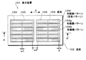
ここで特に、カラー表示が可能な表示装置、例えばフルカラー表示を行う表示装置では、画素(サブピクセル)毎にR(赤)、G(緑)、B(青)の各色に発光する表示素子が配置され、隣接するR,G,Bの3画素で1絵素(ピクセル)が構成される。このような表示装置の製造においては、画素毎に、各色に発光する発光素子を形成する必要がある。このため、例えば有機層パターンの形成工程においては、図5に示すように、基板1上に配列された各画素2のうち、特定の画素2毎に、各発光色の有機層パターン3r,3g,3bを分離形成している。
【0005】
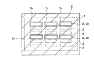
このような各有機層パターン3r,3g,3bの形成は、例えば図6に示すような蒸着マスクを用いた蒸着法によって行われる。この蒸着マスク5は、基板1において画素2が配置される面側に対向して配置され、複数の画素2のうちの特定の色に発光する発光素子が配置される画素(例えば赤)2rのみを露出させる開口部5rを備えている。
【0006】
また、この蒸着マスク5を用いた真空蒸着は、蒸着マスク5の一面側において蒸着源から蒸着材料を蒸発させ状態で、蒸着マスク5の他面側に基板1を配置した状態で行われる。
【0007】
このような蒸着方法の一例として、特開2001−93667号公報には、蒸着源に対して基板および蒸着マスクを移動させる製造装置および製造方法が開示されている。この方法は、図7の模式図に示すように、蒸着空間を仕切るための遮蔽板11に設けられた開口11aの下方に蒸着源12を配置し、この遮蔽板11の上方において、蒸着マスク5とその上部に配置した基板1とを開口11aおよび蒸着源12に対して相対的に移動させながら蒸着を行う方法である。この方法においては、開口11aと蒸着源12とは、基板1および蒸着マスク3の移動方向(図中矢印に示す方向)と直交する方向において、蒸着領域の幅以上の幅を有する線状に設けられている。
【0008】
【発明が解決しようとする課題】
ここで、図8には、前出の図7を、基板1と蒸着マスク5との進行方向から見た図を示す。この図8に示すように、基板1および蒸着マスク5の移動方向と垂直な方向(以下蒸着幅方向と記す)に対しては、蒸着源12は、基板1における蒸着領域と同程度以上の幅に設定されており、またここでの図示を省略した遮蔽板(11)の開口(11a)は、蒸着源12に対応する形状を有している。このため、蒸着源12から蒸着幅方向(蒸着源12の延設方向)に飛散した蒸着成分aは、遮蔽板によってカットされることなく蒸着マスク3を介して基板1に達するのである。
【0009】
したがって、上述したような蒸着方法では、蒸着源12から蒸着幅方向に飛散した蒸着成分aのうち、基板1に対して斜め方向から供給される蒸着成分(斜め蒸着成分)a1も、蒸着マスク5の開口に対して斜め方向から基板1に供給されるため、蒸着マスク3を介して基板1上に蒸着される有機層パターン5r(5gor5b)の膜厚を、蒸着幅方向において均一にすることはできない。図9には、蒸着幅方向における有機層パターン5rの相対膜厚比を示す。この図に示すように、基板の中央部に形成される有機層パターンの相対膜厚比は、その中央部においては一定の膜厚が保たれるものの、蒸着幅方向端部においては斜め蒸着成分a1のみの供給による成膜であるため膜厚が薄くなるのである。また同様の理由により、例えば基板の左端部に形成される有機層パターンの相対膜厚比は、その左端部においては右側からの斜め蒸着成分の侵入のみによる成膜であるため、膜厚が薄くなるのである。
【0010】
ところで、有機層パターンを電極間に挟持してなる発光素子においては、有機層パターンの膜厚が素子の発光特性に大きな影響を与える。このため、各発光素子における発光特性を確保するには、有機層パターンの膜厚が均一な部分のみを発光素子として用いる必要がある。このため、上述したような有機層パターンの端部における相対膜厚比の低下(ばらつき)は、各画素の開口率を低下させる要因となり、表示装置の輝度の向上と、これによる高集積化および高解像度化を妨げる要因となっている。
【0011】
そこで本発明は、電極材料層間に発光材料層を挟持してなる発光素子が設けられた複数の画素を基板上に配列形成してなる表示装置に関し、画素開口率の向上による輝度の向上が可能な表示装置を提供すること、およびこの表示装置の製造に関し、均一な膜厚で材料層の蒸着パターンを形成することが可能な表示装置の製造方法、ならびにこの製造方法に用いる蒸着マスクを提供することを目的とする。
【0012】
【課題を解決するための手段】
以上のような目的を達成するための本発明の表示装置は、下部電極と上部電極との間に発光材料層を挟持してなる発光素子が設けられた複数の画素を、基板上に配列形成してなり、前記上部電極が前記複数の画素に共通に用いられたアクティブマトリックス型の表示装置において、発光素子を構成する材料層のうちの少なくとも1つが蒸着パターンからなり、これらの蒸着パターンが、各画素のうち一方向に隣接して配置された複数の画素を覆う状態で連続的に設けられている。さらに、各蒸着パターンで覆われた画素間の前記一方向の間隔が、当該蒸着パターンのうちの当該一方向に隣接する蒸着パターンで覆われた画素間の当該一方向の間隔よりも狭い。そして、当該一方向に隣接する蒸着パターンで覆われた画素間に、前記上部電極に接続された補助電極が設けられていることを特徴としている。
【0013】
このような表示装置によれば、一方向に隣接する蒸着パターンで覆われた画素間の間隔よりも、同一の蒸着パターン内に一方向に配置された画素間の間隔を狭くすることで、各蒸着パターンの中央部に、その蒸着パターンで覆われた画素が配置されることになる。このため、複数の画素の全てを均等な間隔で配置した場合と比較して、膜厚が安定な蒸着パターンの中央部を有効に利用して複数の画素を配置することができる。したがって、画素の開口率の向上が図られる。また、画素間においてより幅広の間隔部分に補助電極を設けることで、この補助電極が画素の配列に影響を及ぼすことを防止できる。
【0014】
また、本発明の表示装置の製造方法は、電極材料層間に発光材料層を挟持してなる発光素子が設けられた複数の画素を、基板上に配列形成してなる表示装置の製造方法である。本発明においては、蒸着マスクの一面側に蒸着源を配置し、前記蒸着マスクの他面側に前記基板を配置し、蒸着マスクの各開口部から、前記基板における第1方向に配列された複数の画素を一括して露出させた状態で、当該第1方向と直交する第2方向に、前記蒸着マスクと前記基板とを前記蒸着源に対して相対的に移動させることで、前記基板上の各画素に前記発光材料層の蒸着パターンを形成することを特徴としている。
【0015】
このような製造方法によれば、基板および蒸着マスクの移動方向(第2方向)と直交する第1方向に配列された複数の画素を一括して露出させた状態で蒸着が行われるため、この蒸着によって形成される蒸着パターンは、基板における一方向に配列された複数の画素に亘って連続する状態で設けられる。したがって、各画素に対応させて個々の蒸着パターンを形成する場合と比較して、第1方向における蒸着マスクの開口幅が広くなり、基板の第1方向における蒸着パターンの相対膜厚比のばらつきが小さくなる。
【0016】
このような製造方法において、蒸着源の第1方向における幅を、基板の蒸着領域の幅以上とすることで、第1方向に対してより均一に蒸着成分を飛散させ、基板に対してより均一に蒸着成分を入射させることができる。
【0017】
また、このような製造方法において、蒸着マスクと蒸着源との間に、蒸着源に対向する位置に開口を有する遮蔽板を設けることで、第2方向に飛散した蒸着成分のうち、蒸着マスク側に通過する蒸着成分を垂直蒸着成分のみとすることができる。したがって、基板の第2方向における蒸着パターンの相対膜厚比のばらつきが小さくなる。
【0018】
また、本発明の蒸着マスクは、上述した製造方法に用いる蒸着マスクであり、前記基板における一方向に配列された複数の画素を一括して露出させる開口部を備えたことを特徴としている。
【0019】
【発明の実施の形態】
以下、本発明の実施の形態を、図面に基づいて順次詳細に説明する。
【0020】
<表示装置>
図1は、本発明の表示装置の実施形態を示す図であり、図2は図1におけるA−A’断面図である。これらの図に示す表示装置101は、基板102上に複数の画素103を行列状に配列形成してなる、いわゆるストライプ配列の表示装置である。このような表示装置101においては、全ての走査線と信号線が直行するため配線のレイアウトがシンプルであり、また表示画像の鮮明さから、パーソナルコンピュータ用の表示装置としての需要が高い。
【0021】
ここで、各画素103には、基板101側から順に下部電極層(図示省略)、有機層パターン104r,104g,104b、および上部電極層(図示省略)が積層され、これらの層の各積層部分からなる発光素子が設けられている。
【0022】
ここで、有機層パターン104r,104g,104bは、蒸着マスクを用いて形成された蒸着パターンからなり、各発光素子の発光色に対応した材料で形成されている。ここでは、例えば赤(R)、緑(G)、青(B)の各発光色に対応する各有機層パターン104r,104g,104bが、行方向(図面上の横方向)pに配列された2つの画素103,103を覆う状態で設けられる。また、列方向(図面上の縦方向)には、有機層パターン104r、有機層パターン104g、有機層パターン104bが繰り返し配列されている。そして、列方向に配列された3つの画素103によって、1絵素が構成される。
【0023】
ここで、各画素103は、各有機層パターン104r,104g,104bの行方向pにおける中央部に集約され、有機層パターン104r,104g,104bにおける行方向pの端部の、膜厚が不安定な領域dよりも内側に配置されている。そして、1枚の各有機層パターン104r,104g,104bで覆われた画素103間の間隔w1が、行方向pに隣接する有機層パターン104r(104gまたは104b)で覆われた画素103間の間隔w2よりも狭くなっている。
【0024】
また、この表示装置101が、薄膜トランジスタによって各発光素子を駆動させるアクティブマトリックス方式であって、ここでの図示を省略した上部電極が、画素103が配置された領域を全て覆う状態で形成されて各発光素子にわたって共通に用いられている場合には、画素103の間隔が広く設けられている部分(w2部分)に、上部電極の電圧降下を防止するための補助電極を設けるようにする。
【0025】
このような構成の表示装置101においては、行方向pにおいて隣接する有機層パターン104r(104gまたは104b)で覆われた各画素103,103間の間隔w2よりも、同一の有機層パターン104r(104g,104b)内に配置された画素103,103間の間隔w1を狭くすることで、各画素103を、その行方向pにおいて各有機層パターン104r(104g,104b)の中央部に集約して配置している。このため、行方向pに配列された画素103の全てを均等な間隔で配置した場合と比較して、有機層パターン104r(104g,104b)において膜厚が安定している中央部を有効に利用して、行方向pに複数の画素103を配置することができる。また、上述したように、表示装置101がアクティブマトリックス方式であって補助電極を備えている場合、画素103,103間の間隔w2に補助電極を設けることで、この補助電極が画素103の配列に影響を及ぼすことを防止できる。
【0026】
したがって、行方向pにおける画素103の開口率の向上を図ることが可能になる。この結果、輝度の高い表示を行うことが可能になり、さらに輝度を確保して画素数を増加させることができるため、表示装置の高集積化および高解像化を達成することが可能になる。
【0027】
尚、上述した実施形態の表示装置においては、行方向pに配列された2つの画素103,103を一つの有機膜パターン104r(104g,104b)で覆う構成とした。しかし本発明は、行方向pに配列された3つまたはそれ以上の画素103を、一つの有機膜パターン104r(104g,104b)で覆い、各有機層パターン104r(104g,104b)の行方向pにおける中央部にこれらの画素103を集約して配置する構成としても良い。また、各色の有機膜パターン104r,104g,104bの配列が行方向pに繰り返し配列されている場合、行方向pと直行する列方向に配列した複数の画素を一つの有機膜パターン104r(104g,104b)で覆い、各有機層パターン104r(104g,104b)の列方向における中央部にこれらの画素103を集約して配置する構成としても良い。
【0028】
<表示装置の製造方法>
次に、本発明の表示装置の製造方法、およびこの製造方法に用いる蒸着マスクの実施の形態を図面に基づいて詳細に説明する。ここで説明する表示装置の製造方法は、図1を用いて説明した表示装置の製造に適する方法であり、先ず、この製造方法に用いる蒸着マスクの構成を図3に基づき、また図1を参照しつつ説明する。
【0029】
図3に示す実施形態の蒸着マスク201は、いわゆるメタルマスクであり、基板102上に有機層パターン104r,104g,104bを蒸着形成する際に、基板102における画素103配置面側に、基板102に対して所定間隔を保って配置される状態で用いられる。この蒸着マスク201は、各有機層パターン104r,104g,104b毎に用意される。
【0030】
この蒸着マスク201は、例えば有機層パターン104rの形成に用いるものを例に取ると、有機層パターン104rの形成位置に対応する複数の開口部203を有している。各開口部203は、基板102の行方向pに配置される2画素103,103分を露出させる形状を有している。そして、基板102における画素103の配列の列方向において、2つ置き(2行置き)に設けられている。各開口部203の行方向の間隔w3は、蒸着マスク201の撓みを防止できる程度に設定される一方、列方向の間隔w4は、開口部203の列方向の幅w5の2倍程度に設定される。
【0031】
次に、この蒸着マスク201を用いた表示装置の製造方法を、図4の模式図に基づいて説明する。
【0032】
この図に示す表示装置の製造方法は、図1を用いて説明した表示装置の製造方法において、基板102上に有機膜パターン104を形成する場合に適用される方法であり、次のように行われる。
【0033】
すなわち、蒸着装置のチャンバ(図示省略)内を、遮蔽板301によって分離し、この遮蔽板301に形成された開口302aの下方に蒸着源302を配置する。この遮蔽板301には、第1方向xに広い幅を有する長方形の開口302aが設けられている。この開口302aの第1方向xの幅は、基板201の行方向pにおける蒸着領域の幅と同程度以上であることとする。また、蒸着源302は、加熱ホルダとこの内部に充填された蒸着材料(有機層パターンを構成する材料)とで構成されており、遮蔽板301の開口302aと対応する大きさの長方形に形成されている。つまり、この蒸着源302の第1方向xの幅も、開口302aと同程度、すなわち基板201の行方向pにおける蒸着領域の幅と同程度以上であることとする。このような蒸着源302は、開口302aの真下に、開口302aと一致させて配置されている。
【0034】
そして、遮蔽板301の上部には、蒸着マスク201を介して基板102が保持される。これらの蒸着マスク201と基板102とは、ここでの図示を省略した部材によって、所定の間隔に保持された状態を保って、第1方向xと直交する第2方向yに移動する。この際、基板102は、基板102における画素形成面を遮蔽板301側に対向させ、基板102の行方向pを、蒸着源302の長手方向である第1方向xに一致させる。また、蒸着マスク201も、基板102の配置方向に一致させて配置することとし、蒸着マスク201の各開口部203から、基板102の行方向pに配列する複数(例えば2つの画素)を、遮蔽板301側に露出させる。
【0035】
以上のような配置状態において、遮蔽板301および蒸着マスク203を介して基板102の下方に配置された蒸着源302から蒸着材料aを蒸発させる。そして、蒸着マスク201とこの上部に所定状態で配置された基板102とを、これらの配置関係を維持しながら第2方向yへ移動させる。
【0036】
これにより、蒸着マスク201の各開口部203から、基板102の行方向pに配列された複数(2つ)の画素を一括して露出させた状態で、行方向pと直交する第2方向yに、蒸着マスク201と基板102とを相対的に移動させながら、遮蔽板301の開口301aを通過した蒸着材料aを、蒸着マスク201の開口部203を通過させて基板102に蒸着する。この際、遮蔽板301の開口301aおよびこの直下に配置された蒸着源302は、第2方向yと直行する第1方向x、すなわち基板102の行方向pに延設されているため、基板102の行方向における蒸着領域全体に蒸着材料aが供給されることになる。
【0037】
このような製造方法によれば、上述したように基板102および蒸着マスク201の移動方向(第2方向y)と直交する第1方向x(すなわちここでは行方向p)に配列された複数の画素を一括して露出させた状態で蒸着が行われるため、この蒸着によって形成される蒸着パターン(すなわちここでは有機層パターン)は、基板102におけ行方向pに配列された複数の画素に亘って連続する形状に形成される。
【0038】
したがって、各画素に対応させて個々の有機層パターンを形成する場合と比較して、行方向pにおける蒸着マスク201の開口部203の開口幅が広くなり、基板102の行方向pにおける有機層パターンの相対膜厚比のばらつきが小さくなる。つまり、蒸着による有機層パターンの形成においては、発明が解決しようとする課題の項で述べたように、パターンの周縁部が薄膜化する傾向にあるため、有機膜パターンの面積を行方向pに広げることで全体に占める薄膜化部分の面積比が縮小され、これにより相対膜厚比のばらつきを小さくできるのである。
【0039】
したがって、有機層パターンにおける膜厚の安定した部分を有効に利用して画素を配置することで、画素面積を行方向pに広げることが可能になり、輝度の高い表示装置を製造することが可能になる。
【0040】
また、このような製造方法において、遮蔽板301の開口301aと蒸着源302とにおける第1方向xの幅を、基板102の蒸着領域の幅と同程度以上としたので、第1方向xに対してより均一に蒸着成分aを飛散させ、基板102に対してより均一に蒸着成分aを入射させることが可能になる。そして、基板102および蒸着マスク201を第1方向xと直交する第2方向yに移動させるため、1回の移動で基板102の全面に対して蒸着を行うことが可能になり、生産性を確保することも可能である。
【0041】
さらに、遮蔽板301の開口301aと蒸着源302とを対応する大きさの長方形に形成したことで、蒸着源302から第2方向yに飛散した蒸着成分aのうち、蒸着マスク201側に通過する蒸着成分aを、ほぼ垂直蒸着成分のみとすることができる。したがって、基板102の第2方向yにおける有機層パターンの相対膜厚比のばらつきを小さくすることができる。
【0042】
尚、以上説明した各実施形態においては、有機層パターンを蒸着パターンとして形成する場合を例示したが、本発明はこれに限定されることはない。例えば、有機層パターンを挟持する下部電極層または上部電極層が、画素毎に形成される蒸着パターンであって、これらを連続して形成可能である場合、この電極層を上述した構成で形成しても良い。
【0043】
【発明の効果】
以上説明したように、本発明の表示装置によれば、蒸着パターンの中央部にその蒸着パターンで覆われた画素を集約させて配置することで、複数の画素の全てを均等な間隔で配置した場合と比較して、膜厚が安定な蒸着パターンの中央部を有効に利用して複数の画素を配置することができる。したがって、表示装置における画素の開口率の向上を図り、さらに輝度の向上とこれによる高集積化および高解像度化を図ることが可能になる。
【0044】
また、本発明の表示装置の製造方法によれば、基板および蒸着マスクの移動方向と直交する第1方向に配列された複数の画素を一括して露出させた状態で蒸着が行われるため、この蒸着によって形成される蒸着パターンは、基板における一方向に配列された複数の画素に亘って連続する状態で設けられる。したがって、各画素に対応させて個々の蒸着パターンを形成する場合と比較して、第1方向における蒸着マスクの開口幅が広くなり、基板の第1方向における蒸着パターンの相対膜厚比のばらつきを小さくすることが可能になる。この結果、膜厚均一部を利用し、開口率がより大きく輝度の高い表示装置を得ることが可能になる。
【図面の簡単な説明】
【図1】本発明の表示装置の一例を示す平面図である。
【図2】図1のA−A’断面図である。
【図3】本発明の製造方法に用いる蒸着マスクの一例を示す構成図である。
【図4】本発明の製造方法を説明する模式図である。
【図5】従来の表示装置の構成図である。
【図6】従来の製造方法に用いる蒸着マスクの構成図である。
【図7】従来の製造方法を説明する模式図である。
【図8】従来技術の課題を説明するための図である。
【図9】従来技術の課題を説明するための相対膜厚比のグラフである。
【符号の説明】
101…表示装置、102…基板、103…画素、104r,104g,104b…有機層パターン(蒸着パターン)、201…蒸着マスク、203…開口部、301…遮蔽板、301a…開口、302…蒸着源、w1…有機層パターンで覆われた画素間の間隔、w2…隣接する有機層パターンで覆われた画素間の間隔、a…蒸着材料、x…第1方向、y…第2方向[0001]
BACKGROUND OF THE INVENTION
The present invention relates to a display device in which a plurality of light emitting elements are arranged in a matrix, a manufacturing method thereof, and a vapor deposition mask used in the display method.
[0002]
[Prior art]
An organic EL element (organic EL element) using electroluminescence of organic material (hereinafter referred to as EL) has an organic layer sandwiched between an anode and a cathode. In the organic EL element having such a configuration, light generated when holes injected from the anode and electrons injected from the cathode recombine in the organic layer is extracted as emitted light from the cathode or anode side, It attracts attention as a light emitting element capable of emitting light with high brightness of several hundreds to several 10000 cd / m 2 at a low driving voltage of 10 V or less. In addition, in the organic EL element, it is possible to obtain light emitting elements that emit light of each color by selecting the material of the organic layer. By arranging the light emitting elements that emit light of each color in a predetermined state, multicolor display or full color display is achieved. Can be configured.
[0003]
In the case of manufacturing a display device including an organic EL element having such a configuration, first, a lower electrode serving as a cathode (or an anode) is patterned on a substrate, and then an organic layer is formed on the lower electrode. . The formation of the organic layer is usually performed by a vacuum deposition method. In addition, after the organic layer is formed, an upper electrode serving as an anode (or a cathode) is formed in a state in which insulation with the lower electrode is ensured.
[0004]
In particular, in a display device capable of color display, for example, a display device that performs full-color display, a display element that emits light of each color of R (red), G (green), and B (blue) is provided for each pixel (subpixel). One picture element (pixel) is composed of three adjacent R, G, and B pixels. In manufacturing such a display device, it is necessary to form a light emitting element that emits light of each color for each pixel. Therefore, for example, in the organic layer pattern forming step, as shown in FIG. 5, the
[0005]
Such
[0006]
Further, the vacuum deposition using the
[0007]
As an example of such a vapor deposition method, Japanese Patent Application Laid-Open No. 2001-93667 discloses a production apparatus and a production method for moving a substrate and a vapor deposition mask with respect to a vapor deposition source. In this method, as shown in the schematic diagram of FIG. 7, a
[0008]
[Problems to be solved by the invention]
Here, FIG. 8 shows a view of FIG. 7 as seen from the traveling direction of the
[0009]
Therefore, in the vapor deposition method as described above, among the vapor deposition component a scattered in the vapor deposition width direction from the
[0010]
By the way, in a light emitting device in which an organic layer pattern is sandwiched between electrodes, the film thickness of the organic layer pattern greatly affects the light emitting characteristics of the device. For this reason, in order to ensure the light emission characteristic in each light emitting element, it is necessary to use only the part with the uniform film thickness of an organic layer pattern as a light emitting element. For this reason, the decrease (variation) in the relative film thickness ratio at the end of the organic layer pattern as described above becomes a factor that decreases the aperture ratio of each pixel, and improves the luminance of the display device, thereby increasing the integration density. This is a factor preventing high resolution.
[0011]
Therefore, the present invention relates to a display device in which a plurality of pixels provided with a light emitting element having a light emitting material layer sandwiched between electrode material layers are arranged on a substrate, and the luminance can be improved by improving the pixel aperture ratio. The present invention relates to a display device and a method for manufacturing the display device, and a method for manufacturing a display device capable of forming a vapor deposition pattern of a material layer with a uniform film thickness, and a vapor deposition mask used in the method. For the purpose.
[0012]
[Means for Solving the Problems]
In order to achieve the above object, a display device of the present invention is formed by arranging a plurality of pixels provided with a light-emitting element having a light-emitting material layer sandwiched between a lower electrode and an upper electrode on a substrate. Ri greens and, in an active matrix type display device used in common said upper electrode to said plurality of pixels comprises at least one of the deposition pattern of the material layers constituting the light-emitting element, these deposition pattern These are continuously provided so as to cover a plurality of pixels arranged adjacent to each other in one direction . Furthermore, the one-way interval between the pixels covered with each vapor deposition pattern is narrower than the one-way interval between the pixels covered with the vapor deposition pattern adjacent to the one direction among the vapor deposition patterns . An auxiliary electrode connected to the upper electrode is provided between the pixels covered with the vapor deposition pattern adjacent in the one direction .
[0013]
According to such a display device, than the spacing between the pixels covered with deposition patterns adjacent to one direction, by narrowing the spacing between the pixels arranged that in one direction in the same vapor-deposition pattern, each A pixel covered with the vapor deposition pattern is arranged at the center of the vapor deposition pattern. For this reason, compared with the case where all the some pixels are arrange | positioned at equal intervals, a some pixel can be arrange | positioned effectively using the center part of the vapor deposition pattern whose film thickness is stable. Therefore, the aperture ratio of the pixel can be improved. In addition, by providing auxiliary electrodes at wider intervals between the pixels, it is possible to prevent the auxiliary electrodes from affecting the arrangement of the pixels.
[0014]
The display device manufacturing method of the present invention is a method for manufacturing a display device in which a plurality of pixels each provided with a light emitting element having a light emitting material layer sandwiched between electrode material layers are arranged on a substrate. . In the present invention, a deposition source is disposed on one surface side of the deposition mask, the substrate is disposed on the other surface side of the deposition mask, and a plurality of arrays arranged in the first direction of the substrate from each opening of the deposition mask. With the pixels exposed in a lump, the deposition mask and the substrate are moved relative to the deposition source in a second direction orthogonal to the first direction. A vapor deposition pattern of the light emitting material layer is formed on each pixel .
[0015]
According to such a manufacturing method, since the plurality of pixels arranged in the first direction orthogonal to the moving direction (second direction) of the substrate and the deposition mask are exposed in a lump, this deposition is performed. The vapor deposition pattern formed by vapor deposition is provided in a continuous state across a plurality of pixels arranged in one direction on the substrate. Therefore, compared to the case of forming individual vapor deposition patterns corresponding to each pixel, the opening width of the vapor deposition mask in the first direction is widened, and the relative film thickness ratio variation of the vapor deposition pattern in the first direction of the substrate is different. Get smaller.
[0016]
In such a manufacturing method, by setting the width in the first direction of the vapor deposition source to be equal to or larger than the width of the vapor deposition region of the substrate, the vapor deposition components are scattered more uniformly in the first direction, and more uniform with respect to the substrate. The vapor deposition component can be incident on the substrate.
[0017]
Moreover, in such a manufacturing method, by providing a shielding plate having an opening at a position facing the vapor deposition source between the vapor deposition mask and the vapor deposition source, the vapor deposition mask side of the vapor deposition components scattered in the second direction. Only the vertical vapor deposition component can pass through the vapor deposition component. Therefore, the variation in the relative film thickness ratio of the vapor deposition pattern in the second direction of the substrate is reduced.
[0018]
The vapor deposition mask of the present invention is a vapor deposition mask used in the above-described manufacturing method, and is characterized in that it has an opening that collectively exposes a plurality of pixels arranged in one direction on the substrate.
[0019]
DETAILED DESCRIPTION OF THE INVENTION
DESCRIPTION OF EMBODIMENTS Hereinafter, embodiments of the present invention will be sequentially described in detail based on the drawings.
[0020]
<Display device>
FIG. 1 is a diagram showing an embodiment of a display device of the present invention, and FIG. 2 is a cross-sectional view taken along line AA ′ in FIG. The display device 101 shown in these drawings is a so-called stripe array display device in which a plurality of
[0021]
Here, in each
[0022]
Here, the
[0023]
Here, each
[0024]
In addition, the display device 101 is an active matrix system in which each light emitting element is driven by a thin film transistor, and an upper electrode (not shown) is formed so as to cover the entire region where the
[0025]
In the display device 101 having such a configuration, the same
[0026]
Therefore, it is possible to improve the aperture ratio of the
[0027]
In the display device of the above-described embodiment, the two
[0028]
<Manufacturing method of display device>
Next, an embodiment of a manufacturing method of a display device of the present invention and a vapor deposition mask used in the manufacturing method will be described in detail with reference to the drawings. The manufacturing method of the display device described here is a method suitable for manufacturing the display device described with reference to FIG. 1. First, the configuration of the vapor deposition mask used in this manufacturing method is based on FIG. 3, and also refer to FIG. However, it will be explained.
[0029]
The
[0030]
For example, when the
[0031]
Next, the manufacturing method of the display apparatus using this
[0032]
The display device manufacturing method shown in this figure is a method applied when the organic film pattern 104 is formed on the
[0033]
That is, the inside of the chamber (not shown) of the vapor deposition apparatus is separated by the shielding plate 301, and the vapor deposition source 302 is disposed below the opening 302 a formed in the shielding plate 301. The shielding plate 301 is provided with a rectangular opening 302a having a wide width in the first direction x. The width of the opening 302a in the first direction x is equal to or larger than the width of the vapor deposition region in the row direction p of the
[0034]
The
[0035]
In the arrangement state as described above, the vapor deposition material a is evaporated from the vapor deposition source 302 disposed below the
[0036]
As a result, a plurality of (two) pixels arranged in the row direction p of the
[0037]
According to such a manufacturing method, as described above, a plurality of pixels arranged in the first direction x (that is, the row direction p here) orthogonal to the moving direction (second direction y) of the
[0038]
Therefore, the opening width of the
[0039]
Therefore, it is possible to expand the pixel area in the row direction p by effectively using the portion having a stable film thickness in the organic layer pattern, and it is possible to manufacture a display device with high luminance. become.
[0040]
In such a manufacturing method, the width in the first direction x in the opening 301a of the shielding plate 301 and the vapor deposition source 302 is set to be equal to or greater than the width of the vapor deposition region in the
[0041]
Furthermore, by forming the opening 301a of the shielding plate 301 and the vapor deposition source 302 into a corresponding rectangular shape, the vapor deposition component a scattered in the second direction y from the vapor deposition source 302 passes through the
[0042]
In addition, in each embodiment demonstrated above, although the case where an organic layer pattern was formed as a vapor deposition pattern was illustrated, this invention is not limited to this. For example, when the lower electrode layer or the upper electrode layer sandwiching the organic layer pattern is a vapor deposition pattern formed for each pixel and can be continuously formed, the electrode layer is formed with the above-described configuration. May be.
[0043]
【The invention's effect】
As described above, according to the display device of the present invention, by arranging the pixels covered with the vapor deposition pattern in the central portion of the vapor deposition pattern, all of the plurality of pixels are arranged at equal intervals. Compared to the case, a plurality of pixels can be arranged by effectively using the central portion of the vapor deposition pattern having a stable film thickness. Accordingly, it is possible to improve the aperture ratio of the pixel in the display device, further improve the luminance, and thereby achieve higher integration and higher resolution.
[0044]
In addition, according to the method for manufacturing a display device of the present invention, since the plurality of pixels arranged in the first direction orthogonal to the moving direction of the substrate and the vapor deposition mask are collectively exposed, this is performed. The vapor deposition pattern formed by vapor deposition is provided in a continuous state across a plurality of pixels arranged in one direction on the substrate. Therefore, compared to the case of forming individual vapor deposition patterns corresponding to each pixel, the opening width of the vapor deposition mask in the first direction is widened, and the variation in the relative film thickness ratio of the vapor deposition pattern in the first direction of the substrate is caused. It becomes possible to make it smaller. As a result, it is possible to obtain a display device having a larger aperture ratio and higher luminance by utilizing the uniform thickness portion.
[Brief description of the drawings]
FIG. 1 is a plan view illustrating an example of a display device of the present invention.
FIG. 2 is a cross-sectional view taken along the line AA ′ in FIG.
FIG. 3 is a configuration diagram showing an example of a vapor deposition mask used in the manufacturing method of the present invention.
FIG. 4 is a schematic diagram for explaining the production method of the present invention.
FIG. 5 is a configuration diagram of a conventional display device.
FIG. 6 is a configuration diagram of a vapor deposition mask used in a conventional manufacturing method.
FIG. 7 is a schematic diagram for explaining a conventional manufacturing method.
FIG. 8 is a diagram for explaining a problem of the prior art.
FIG. 9 is a graph of a relative film thickness ratio for explaining a problem of the prior art.
[Explanation of symbols]
DESCRIPTION OF SYMBOLS 101 ... Display apparatus, 102 ... Board | substrate, 103 ... Pixel, 104r, 104g, 104b ... Organic layer pattern (deposition pattern), 201 ... Deposition mask, 203 ... Opening part, 301 ... Shielding plate, 301a ... Opening, 302 ... Deposition source , W1 ... interval between pixels covered with organic layer pattern, w2 ... interval between pixels covered with adjacent organic layer pattern, a ... deposition material, x ... first direction, y ... second direction
Claims (2)
前記発光素子を構成する材料層のうちの少なくとも1つが蒸着パターンからなり、当該蒸着パターンが前記画素のうち一方向に隣接して配置された複数の画素を覆う状態で連続的に設けられ、
前記各蒸着パターンで覆われた画素間の前記一方向の間隔が、当該蒸着パターンのうちの当該一方向に隣接する蒸着パターンで覆われた画素間の当該一方向の間隔よりも狭く、
前記一方向に隣接する蒸着パターンで覆われた画素間に、前記上部電極に接続された補助電極が設けられている
ことを特徴とする表示装置。A plurality of pixels provided with a light emitting element having a light emitting material layer sandwiched between a lower electrode and an upper electrode are arranged on a substrate, and the upper electrode is commonly used for the plurality of pixels. In an active matrix type display device,
At least one of the material layers constituting the light emitting element is composed of a vapor deposition pattern, and the vapor deposition pattern is continuously provided in a state of covering a plurality of pixels arranged adjacent to one direction among the pixels,
The one-way interval between the pixels covered with the respective vapor deposition patterns is narrower than the one-way interval between the pixels covered with the vapor deposition pattern adjacent to the one direction of the vapor deposition patterns,
An auxiliary electrode connected to the upper electrode is provided between the pixels covered with the vapor deposition pattern adjacent in the one direction .
前記蒸着パターンは、前記下部電極と上部電極との間に挟持された有機層パターンからなる The vapor deposition pattern includes an organic layer pattern sandwiched between the lower electrode and the upper electrode.
ことを特徴とする表示装置。 A display device characterized by that.
Priority Applications (1)
| Application Number | Priority Date | Filing Date | Title |
|---|---|---|---|
| JP2002001052A JP4089228B2 (en) | 2002-01-08 | 2002-01-08 | Display device |
Applications Claiming Priority (1)
| Application Number | Priority Date | Filing Date | Title |
|---|---|---|---|
| JP2002001052A JP4089228B2 (en) | 2002-01-08 | 2002-01-08 | Display device |
Publications (3)
| Publication Number | Publication Date |
|---|---|
| JP2003203767A JP2003203767A (en) | 2003-07-18 |
| JP2003203767A5 JP2003203767A5 (en) | 2005-06-23 |
| JP4089228B2 true JP4089228B2 (en) | 2008-05-28 |
Family
ID=27641269
Family Applications (1)
| Application Number | Title | Priority Date | Filing Date |
|---|---|---|---|
| JP2002001052A Expired - Fee Related JP4089228B2 (en) | 2002-01-08 | 2002-01-08 | Display device |
Country Status (1)
| Country | Link |
|---|---|
| JP (1) | JP4089228B2 (en) |
Families Citing this family (2)
| Publication number | Priority date | Publication date | Assignee | Title |
|---|---|---|---|---|
| JP2012104300A (en) * | 2010-11-09 | 2012-05-31 | Hitachi Displays Ltd | Organic electroluminescent panel and manufacturing method thereof |
| JP5812753B2 (en) * | 2011-08-11 | 2015-11-17 | 株式会社アルバック | Film forming apparatus and film forming method |
-
2002
- 2002-01-08 JP JP2002001052A patent/JP4089228B2/en not_active Expired - Fee Related
Also Published As
| Publication number | Publication date |
|---|---|
| JP2003203767A (en) | 2003-07-18 |
Similar Documents
| Publication | Publication Date | Title |
|---|---|---|
| US11522152B2 (en) | Display panel and fabrication method thereof, and display apparatus | |
| JP3620490B2 (en) | Active matrix display device | |
| KR100518709B1 (en) | Method of attaching layer material and forming layer in predetermined pattern on substrate using mask | |
| KR101065314B1 (en) | Organic light emitting display apparatus | |
| KR101479994B1 (en) | Organic light emitting diode display and method for manufacturing the same | |
| US5742129A (en) | Organic electroluminescent display panel with projecting ramparts and method for manufacturing the same | |
| JP4925566B2 (en) | Shadow mask | |
| TWI413448B (en) | Method of depositing light emitting layer of organic el device, method of manufacturing organic el device, and organic el device manufactured by the method | |
| JP2002215063A (en) | Active matrix type display device | |
| KR101097305B1 (en) | Fine deposition mask providing block unit to block dummy slit unit, the manufacturing method of organic light emitting device using the same mask, and the organic light emitting device which is manufactured by the same method | |
| WO2021227710A1 (en) | Display panel and manufacturing method therefor, and display device | |
| US20220376204A1 (en) | Methods and apparatus for organic light emitting diode display structures | |
| JP2760347B2 (en) | Organic thin film electroluminescent device and method of manufacturing the same | |
| JP2000100576A (en) | Organic el display | |
| WO2022199003A1 (en) | Pixel arrangement structure, and display panel and method for preparing same | |
| JP2018006232A (en) | Display device and manufacturing method thereof | |
| JP4789341B2 (en) | Semiconductor device and mask for manufacturing semiconductor device | |
| US6224448B1 (en) | Luminescent display device and method of forming the same | |
| JP4089228B2 (en) | Display device | |
| US20070290955A1 (en) | Organic electroluminescent display device and manufacturing method thereof | |
| US11195892B2 (en) | Electroluminescence display device and manufacturing method thereof | |
| JP4789340B2 (en) | Semiconductor device and mask for manufacturing semiconductor device | |
| CN215220728U (en) | Pixel arrangement structure, display panel and display device | |
| US11958073B2 (en) | Deposition device and deposition method | |
| US20230220548A1 (en) | Deposition device and deposition method |
Legal Events
| Date | Code | Title | Description |
|---|---|---|---|
| A521 | Request for written amendment filed |
Free format text: JAPANESE INTERMEDIATE CODE: A523 Effective date: 20040927 |
|
| A621 | Written request for application examination |
Free format text: JAPANESE INTERMEDIATE CODE: A621 Effective date: 20040927 |
|
| A977 | Report on retrieval |
Free format text: JAPANESE INTERMEDIATE CODE: A971007 Effective date: 20070405 |
|
| A131 | Notification of reasons for refusal |
Free format text: JAPANESE INTERMEDIATE CODE: A131 Effective date: 20070410 |
|
| A521 | Request for written amendment filed |
Free format text: JAPANESE INTERMEDIATE CODE: A523 Effective date: 20070611 |
|
| A131 | Notification of reasons for refusal |
Free format text: JAPANESE INTERMEDIATE CODE: A131 Effective date: 20071002 |
|
| A521 | Request for written amendment filed |
Free format text: JAPANESE INTERMEDIATE CODE: A523 Effective date: 20071128 |
|
| TRDD | Decision of grant or rejection written | ||
| A01 | Written decision to grant a patent or to grant a registration (utility model) |
Free format text: JAPANESE INTERMEDIATE CODE: A01 Effective date: 20080205 |
|
| A61 | First payment of annual fees (during grant procedure) |
Free format text: JAPANESE INTERMEDIATE CODE: A61 Effective date: 20080218 |
|
| FPAY | Renewal fee payment (event date is renewal date of database) |
Free format text: PAYMENT UNTIL: 20110307 Year of fee payment: 3 |
|
| FPAY | Renewal fee payment (event date is renewal date of database) |
Free format text: PAYMENT UNTIL: 20110307 Year of fee payment: 3 |
|
| LAPS | Cancellation because of no payment of annual fees |