JP4085798B2 - Wafer position teaching method, teaching jig, and robot - Google Patents
Wafer position teaching method, teaching jig, and robot Download PDFInfo
- Publication number
- JP4085798B2 JP4085798B2 JP2002359389A JP2002359389A JP4085798B2 JP 4085798 B2 JP4085798 B2 JP 4085798B2 JP 2002359389 A JP2002359389 A JP 2002359389A JP 2002359389 A JP2002359389 A JP 2002359389A JP 4085798 B2 JP4085798 B2 JP 4085798B2
- Authority
- JP
- Japan
- Prior art keywords
- teaching
- semiconductor wafer
- robot
- wafer
- cone
- Prior art date
- Legal status (The legal status is an assumption and is not a legal conclusion. Google has not performed a legal analysis and makes no representation as to the accuracy of the status listed.)
- Expired - Fee Related
Links
Images


Description
【0001】
【発明の属する技術分野】
本発明は、半導体ウェハ搬送用ロボットに半導体ウェハの位置を教示する方法に関するものである。また前記方法に用いる教示用治具に関するものである。
【0002】
【従来の技術】
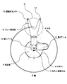
半導体ウェハ搬送用ロボットに半導体ウェハの位置を教示する従来の方法は、次のような手順で行なわれている。すなわち、円盤部とその円盤部の中心もしくは中心よりずれた位置に立設されたピンを持つ教示用冶具を収納容器あるいは処理装置の半導体ウェハを設置する位置に設置し、教示用冶具の円盤部のエッジを検知手段を用いて検出し、また前記教示用冶具のピンの位置を検知手段を用いて検出しその検出位置に基づいて前記教示用冶具の中心位置を検知してポジションデータを取得し記憶する。この方法では、図9に示すように検知手段1がピン2からの反射光に基づきピン2のX(前後)方向の位置3を検出する。また図10に示すように検知手段1からレーザ光Rを旋回照射して、反射光の有無からピン2の左右両端を検知し、その2等分位置をY(旋回)方向の位置4として検出する。また図11に示すように検知手段1からレーザ光RをZ(上下)方向へ上下動照射して反射光の有無から円盤部5のエッジを検知し、その位置を教示用冶具6のZ(高さ)方向の位置7として検出するという手順がとられていた(例えば特許文献1)。
【0003】
【特許文献1】
特開平9−102527号公報
【0004】
【発明が解決しようとする課題】
しかしながら、従来の方法では、収納容器及び処理装置の形状によってはZ(高さ)方向にロボットを動作させることが困難なことがある。例えば、教示位置周辺に障害物があり検出手段によるセンシングが行えない場合や、また検出手段がウェハ把持部に取り付けられている場合は収納容器及び処理装置の間口が狭いことでZ方向の動作が制限される為、エッジを検出することができない可能性がある。
本発明はこのような様々な問題点に鑑みてなされたものであり、ステーションに置載した教示用冶具の特徴部(センシング対象)を円錐または円錐の特徴を有する形状にすることにより、その円錐断面の径を検出することで Z(高さ)方向のエッジを検出することなく、教示用冶具のZ(高さ)方向を検出する方法を提供することを目的とするものである。
【0005】
【課題を解決するための手段】
上記の課題を解決するために、請求項1の発明は、収納容器と処理装置の間あるいは処理装置相互の間で半導体ウェハの搬送を行なうロボットに前記半導体ウェハの位置を教示するウェハ位置教示方法において、前記収納容器あるいは前記処理装置の半導体ウェハを設置する位置に教示用治具を設置し、前記教示用治具上の中心軸部に円錐または円錐の特徴を有する形状部を設け、前記ロボットのハンドの先端に設けた透過式センサで前記円錐部を検出し、前記円錐部の断面径に基づき、前記教示用冶具のZ(高さ)方向を検出することを特徴とする。
また請求項2の発明は、収納容器と処理装置の間あるいは処理装置相互の間で半導体ウェハの搬送を行なうロボットに前記半導体ウェハの位置を教示するウェハ位置教示方法において、前記収納容器あるいは前記処理装置の半導体ウェハを設置する位置との関係が明らかになっている位置に、円錐または円錐の特徴を有する形状部を設け、前記ロボットのハンドの先端に設けた透過式センサで前記円錐部を検出し、前記円錐部の断面径に基づき、半導体ウェハを設置する位置のZ(高さ)方向を検出することを特徴とする。
また請求項3の発明は、収納容器と処理装置の間あるいは処理装置相互の間で半導体ウェハの搬送を行なうロボットに前記半導体ウェハの位置を教示する教示用治具において、前記半導体ウェハと同一の外径を有する大円板部と、前記大円板部と中心軸を共通にする円錐または円錐の特徴を有する形状部を持つことを特徴とする。
このようになっているため、ロボットの動作範囲(Z方向)に制限がある場合でも、位置の教示ができ、半導体ウェハの設置位置の教示ができ、教示用治具を設置する際の回転方向の向きは所定の角度ずれても問題がなく、教示用治具の設置が容易になるのである
【0006】
【発明の実施の形態】
以下、本発明の方法の具体的実施例について、図に基づいて説明する。
図1および図2は本発明の実施例を示すロボットの平面図であり、図3は側面図である。図において、8は半導体ウェハ搬送用の水平多関節型ロボットであり、Wはロボット8の搬送対象の半導体ウェハである。ロボット8は、昇降自在な円柱状の支柱部9の中心軸14回りに水平面内で旋回する第1アーム10と、第1アーム10の先端に水平面内で旋回自在に取り付けられた第2アーム11と、第2アーム11の先端に水平面内で旋回自在に取り付けられたウェハ把持部12を備えている。ウェハ把持部12は半導体ウェハWを載置するY字形のハンドであって、Y字形の先端に1組の透過式センサ13を備えている。
【0007】
図に示すように、ロボット8は第1アーム10、第2アーム11およびウェハ把持部12の相対的な角度を保ったまま、第1アーム10を支柱部9の中心軸14回りに旋回させるθ軸動作(旋回)、第1アーム10、第2アーム11およびウェハ把持部12を一定の速度比を保って旋回させることにより、ウェハ把持部12を支柱部9の半径方向に伸縮させるR軸動作(伸縮)、および支柱部9を昇降させるZ軸動作(昇降)の3自由度を有している。
ここで、θ軸は反時計回りをプラス方向とし(図1参照)、R軸は、ウェハ把持部12を支柱部9から遠ざける方向、つまりアームを伸ばす方向をプラスとし(図2参照)、Z軸は、支柱部9を上昇させる方向をプラス(図3参照)とする。
【0008】
図4は本発明の実施例を示す透過式センサの説明図である。図において、15はY字形のウェハ把持部12の一方の端に取り付けられた発光部であり、16は他方の端に発光部15に対向するように取り付けられた受光部である。発光部15と受光部16で1組の透過式センサ13を構成している。17は発光部15から受光部16に向かう光軸であり、透過式センサ13は光軸17を遮る物体を検出することができる。
【0009】
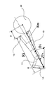
図5および図6は本発明の実施例を示すウェハ位置教示方法の説明図である。図において、18は大円板部19と円錐部20の中心を一致させて上下に重ねて結合した教示用治具である。大円板部19の直径は実物の半導体ウェハに等しく、収納容器等の半導体ウェハを載置する場所に大円板部19を載置することができる。また円錐部20の形状は、事前に測定されているので、円錐部20の断面径を知ればその断面の位置から大円盤部19までの高さ方向の距離を知ることができる。また大円板部19と円錐部20の相対位置は、事前に測定されているので、円錐部20の位置を知れば大円板部19の位置を知ることができる。
なお、大円板部19の厚さは約2mmであり、実物の半導体ウェハの厚さ0.7mmより大きいが、これは強度上の制約から決められたものであり、実物の半導体ウェハの厚さと同一にしたほうが望ましいことは言うまでもない。
【0010】
次に、ウェハ位置教示方法の手順を説明する。
(ステップ1)教示治具18を収納容器等の半導体ウェハを載置する場所に載置する。大円板部19は実物の半導体ウェハと全く同一の外径を有するから、収納容器等の位置決めガイド等により、教示冶具18は正しく位置決めさせる。
(ステップ2)作業者の操作により、図6に示すように、ウェハ把持部12を光軸17が円錐部20を遮る高さに移動させる。
(ステップ3)ウェハ把持部12を移動させ、円錐部20の手前を透過式センサ13で検出し、その時のR軸の座標R1を記録する。さらにウェハ把持部12を移動させ円錐部20の奥を透過式センサ13で検出し、その時のR軸の座標R2を記録する。
(ステップ4)円錐部20の断面径を(R2−R1)にする。すでに円錐部の形状は測定されているので円錐部20の断面径より大円盤部から円錐部の断面までの高さを知ることができる。つまり、教示冶具18のZ(高さ)方向の位置を円錐部断面の高さ方向の位置より算出し設定する。
(ステップ5)R軸を動作させて、透過式センサ13が円錐部20を検出しない位置までアームを縮める。
(ステップ6)θ軸を動作させて、ウェハ把持部12の向きを変え、次にR軸を動作させて、ウェハ把持部12を円錐部20にゆっくり接近させる。そして透過式センサ13が円錐部20を最初に検出した時、すなわち光軸17が円錐部20の円周に接した時、のθ軸とR軸の座標を記録する。
(ステップ7)ステップ5とステップ6を繰り返して、ウェハ把持部12を異なる方向から円錐部20に接近させ、光軸17が円錐部20の円周に接する時のθ軸とR軸の座標を複数組求める。そして、これらの値から、円錐部20の中心の位置を求めて記録する。
【0011】
以上のようにして、円錐部20の位置が求まる。円錐部20と大円板部19の相対的な位置関係は事前に測定されているから、この位置関係分だけ前記位置をシフトすれば、大円板部19の位置すなわち、収納容器等に載置された半導体ウェハの位置が求まるわけである。
また、ステップ2からステップ7までの操作を予め、プログラムしておけば、半導体ウェハの位置の教示を、作業者の操作に拠らず、自動的に行なうことができる。
【0012】
次に、ステップ3ないしステップ7において、円錐部20のセンシングを行った高さを求める計算手順と、円錐部20の中心座標(θs,Rs)を求める計算の手順の詳細を説明する。図7はステップ3において、光軸17が円錐20を横切る状態を示す説明図である。H、Lは教示用冶具18上の円錐20の高さと底面の直径をあらわす。R1とR2は光軸17が円錐20を横切った時の伸縮方向の座標である。光軸17が円錐を横切った断面の直径をL1とすると、下記の式が成り立つ。
【0013】
L1=R2-R1 (1)
ここで、円錐20の形状は既に測定されており、高さH、底面の直径Lより
H:L=H1:L1 (2)
これより、H2は
H1=(R2-R1)・H/L (3)
H2=H-H1 (4)
となる。
【0014】
図8はステップ6において、光軸17が円錐部20の円周に接した状態を示す説明図である。θi、Riは透過式センサ6の光軸17が円錐部20の円周に接した時のロボット1のθ軸およびR軸の座標である。Rmは光軸17と円錐部20の円周の接点と第1アーム10の旋回中心の距離であり、rは円錐部20を光軸17をもってセンシングし検出した半径であるとすると、下記の式が成り立つ。
【0015】
Ri+r=(Rm+r)・cos(θi-θs) (5)
ここで、Rs=Rm+rだから、
Ri+r=Rs・cos(θi-θs) (6)
変形すると、
Ri+r=Rs・cosθs・cosθi+Rs・sinθs・sinθi (7)
ここで、A=Rs・cosθs,B=Rs・sinθsとおくと、下記の式が得られる。
Ri+r=A・cosθi+B・sinθi (8)
【0016】
ここで、ステップ7で説明したように、ウェハ把持部12の向きを変えて、計測を繰り返して、θi、Riの値を3組以上求めて、最小2乗法を用いて係数A,Bを決定する。
係数A,Bが決定するとθsは下記の式で得られる。
θs=tan-1(B/A) (9)
また、cosθs=A/(A2+B2)0.5だから、Rsは下記の式で得られる。
Rs=(A2+B2) 0.5 (10)
【0017】
【発明の効果】
以上述べたように、請求項1、3の発明によれば、教示用治具の円錐部の断面径をハンド上のセンサで検出することにより、教示用冶具のZ(高さ)方向を検出できるので、ロボットの動作範囲(Z方向)に制限がある場合でも、位置の教示ができるという効果がある。また請求項2の発明によれば、半導体ウェハを設置する位置との関係が明らかな円錐部の断面径をハンド上のセンサで検出することにより、半導体ウェハ設置位置の教示ができるという効果がある。また請求項3の発明によれば、教示用治具の形状は中心軸を共通とする形状物から構成しているので、教示用治具を設置する際の回転方向の向きは所定の角度ずれても問題ないので、教示用治具の設置が容易であるという効果がある。
【図面の簡単な説明】
【図1】本発明の実施例を示すロボットの平面図である。
【図2】本発明の実施例を示すロボットの別の平面図である。
【図3】本発明の実施例を示すロボットの側面図である。
【図4】本発明の実施例を示す透過式センサの説明図である。
【図5】本発明の実施例を示すウェハ位置教示方法の説明図である。
【図6】本発明の実施例を示すウェハ位置教示方法の説明図である。
【図7】本発明の実施例を示すウェハ位置教示方法の説明図である。
【図8】本発明の実施例を示すウェハ位置教示方法の説明図である。
【図9】従来の技術の実施例を示すウェハ位置教示方法の説明図である。
【図10】従来の技術の実施例を示すウェハ位置教示方法の説明図である。
【図11】従来の技術の実施例を示すウェハ位置教示方法の説明図である。
【符号の説明】
1.検知手段、2.ピン、3.X(前後)方向の位置、4.Y(旋回)方向の位置、5.円盤部、6.教示用冶具、7.Z(高さ)方向の位置、8.ロボット、9.支柱部、10.第1アーム、11.第2アーム、12.ウェハ把持部、13.透過式センサ、14.ロボット旋回中心、15.発光部、16.受光部、17.光軸、18.教示治具、19.大円板部、20.円錐部、[0001]
BACKGROUND OF THE INVENTION
The present invention relates to a method for teaching a position of a semiconductor wafer to a semiconductor wafer transfer robot. The present invention also relates to a teaching jig used in the above method.
[0002]
[Prior art]
A conventional method for teaching a position of a semiconductor wafer to a semiconductor wafer transfer robot is performed in the following procedure. In other words, a teaching jig having a disk part and a pin erected at the center of the disk part or a position shifted from the center is installed at a position where a semiconductor wafer of a storage container or a processing apparatus is installed, and the disk part of the teaching jig The edge of the teaching jig is detected using the detecting means, the position of the pin of the teaching jig is detected using the detecting means, and the center position of the teaching jig is detected based on the detected position to obtain position data. Remember. In this method, as shown in FIG. 9, the detection means 1 detects the position 3 of the pin 2 in the X (front-rear) direction based on the reflected light from the pin 2. Further, as shown in FIG. 10, the laser beam R is radiated from the detection means 1 to detect the left and right ends of the pin 2 based on the presence or absence of reflected light, and the bisected position is detected as the position 4 in the Y (turning) direction. To do. Further, as shown in FIG. 11, the laser beam R is vertically moved in the Z (vertical) direction from the detecting means 1 to detect the edge of the
[0003]
[Patent Document 1]
JP-A-9-102527 [0004]
[Problems to be solved by the invention]
However, in the conventional method, it may be difficult to operate the robot in the Z (height) direction depending on the shapes of the storage container and the processing apparatus. For example, when there is an obstacle around the teaching position and sensing by the detection means cannot be performed, or when the detection means is attached to the wafer gripping part, the operation in the Z direction is performed due to the narrow opening between the storage container and the processing apparatus. Because it is limited, there is a possibility that the edge cannot be detected.
The present invention has been made in view of such various problems. By forming a feature (sensing target) of a teaching jig mounted on a station into a shape having a cone or a cone, the cone is obtained. An object of the present invention is to provide a method for detecting the Z (height) direction of a teaching jig without detecting an edge in the Z (height) direction by detecting the diameter of the cross section.
[0005]
[Means for Solving the Problems]
In order to solve the above-mentioned problems, the invention of claim 1 is directed to a wafer position teaching method for teaching a position of the semiconductor wafer to a robot that transports the semiconductor wafer between the storage container and the processing apparatus or between the processing apparatuses. A teaching jig is installed at a position where the storage container or the semiconductor wafer of the processing apparatus is installed, and a cone or a shape part having a conical feature is provided on a central axis portion on the teaching jig, and the robot The cone portion is detected by a transmission type sensor provided at the tip of the hand, and the Z (height) direction of the teaching jig is detected based on the cross-sectional diameter of the cone portion.
According to a second aspect of the present invention, there is provided a wafer position teaching method for teaching a position of a semiconductor wafer to a robot that transfers a semiconductor wafer between a storage container and a processing apparatus or between processing apparatuses. At the position where the relationship with the position where the semiconductor wafer of the device is installed is clarified, a cone or a shape part having a cone shape is provided, and the cone part is detected by a transmission sensor provided at the tip of the robot hand. The Z (height) direction of the position where the semiconductor wafer is installed is detected based on the cross-sectional diameter of the conical portion.
According to a third aspect of the present invention, there is provided a teaching jig for teaching a position of the semiconductor wafer to a robot that transfers the semiconductor wafer between the storage container and the processing apparatus or between the processing apparatuses. A large disc portion having an outer diameter and a shape portion having a conical shape or a conical feature sharing a central axis with the large disc portion.
This makes it possible to teach the position even when the robot's movement range (Z direction) is limited, to teach the installation position of the semiconductor wafer, and to rotate when the teaching jig is installed There is no problem even if the orientation of the lens is deviated by a predetermined angle, and the teaching jig can be easily installed.
DETAILED DESCRIPTION OF THE INVENTION
Hereinafter, specific examples of the method of the present invention will be described with reference to the drawings.
1 and 2 are plan views of a robot showing an embodiment of the present invention, and FIG. 3 is a side view. In the figure, 8 is a horizontal articulated robot for transferring a semiconductor wafer, and W is a semiconductor wafer to be transferred by the robot 8. The robot 8 includes a
[0007]
As shown in the figure, the robot 8 turns the
Here, the θ-axis is a counterclockwise plus direction (see FIG. 1), and the R-axis is a plus direction in which the
[0008]
FIG. 4 is an explanatory diagram of a transmissive sensor showing an embodiment of the present invention. In the figure, 15 is a light emitting part attached to one end of a Y-shaped
[0009]
5 and 6 are explanatory views of a wafer position teaching method showing an embodiment of the present invention. In the figure,
The thickness of the
[0010]
Next, the procedure of the wafer position teaching method will be described.
(Step 1) The
(Step 2) By the operator's operation, the
(Step 3) The
(Step 4) The cross-sectional diameter of the
(Step 5) The R axis is operated to retract the arm to a position where the
(Step 6) The θ axis is operated to change the orientation of the
(Step 7) Steps 5 and 6 are repeated to bring the
[0011]
As described above, the position of the
If the operations from step 2 to step 7 are programmed in advance, the position of the semiconductor wafer can be automatically taught without depending on the operator's operation.
[0012]
Next, details of a calculation procedure for obtaining the height at which the
[0013]
L1 = R2-R1 (1)
Here, the shape of the
H: L = H1: L1 (2)
From this, H2
H1 = (R2-R1) ・ H / L (3)
H2 = H-H1 (4)
It becomes.
[0014]
FIG. 8 is an explanatory diagram showing a state in which the
[0015]
Ri + r = (Rm + r) ・ cos (θi-θs) (5)
Where Rs = Rm + r,
Ri + r = Rs ・ cos (θi-θs) (6)
When deformed,
Ri + r = Rs ・ cosθs ・ cosθi + Rs ・ sinθs ・ sinθi (7)
Here, when A = Rs · cos θs and B = Rs · sin θs, the following equations are obtained.
Ri + r = A ・ cosθi + B ・ sinθi (8)
[0016]
Here, as described in step 7, the orientation of the
When the coefficients A and B are determined, θs is obtained by the following equation.
θs = tan -1 (B / A) (9)
Also, since cos θs = A / (A2 + B2) 0.5 , Rs can be obtained by the following equation.
Rs = (A2 + B2) 0.5 (10)
[0017]
【The invention's effect】
As described above, according to the first and third aspects of the invention, the Z (height) direction of the teaching jig is detected by detecting the cross-sectional diameter of the conical portion of the teaching jig with the sensor on the hand. Therefore, there is an effect that the position can be taught even when the operation range (Z direction) of the robot is limited. According to the second aspect of the present invention, there is an effect that the position of the semiconductor wafer can be taught by detecting the cross-sectional diameter of the conical portion having a clear relationship with the position of installing the semiconductor wafer with the sensor on the hand. . According to the invention of claim 3, since the shape of the teaching jig is formed of a shape having a common central axis, the direction of the rotation direction when the teaching jig is installed is shifted by a predetermined angle. However, since there is no problem, there is an effect that the teaching jig can be easily installed.
[Brief description of the drawings]
FIG. 1 is a plan view of a robot showing an embodiment of the present invention.
FIG. 2 is another plan view of the robot showing the embodiment of the present invention.
FIG. 3 is a side view of a robot showing an embodiment of the present invention.
FIG. 4 is an explanatory diagram of a transmissive sensor showing an embodiment of the present invention.
FIG. 5 is an explanatory diagram of a wafer position teaching method showing an embodiment of the present invention.
FIG. 6 is an explanatory diagram of a wafer position teaching method showing an embodiment of the present invention.
FIG. 7 is an explanatory diagram of a wafer position teaching method showing an embodiment of the present invention.
FIG. 8 is an explanatory diagram of a wafer position teaching method showing an embodiment of the present invention.
FIG. 9 is an explanatory diagram of a wafer position teaching method showing an embodiment of the prior art.
FIG. 10 is an explanatory view of a wafer position teaching method showing an embodiment of the prior art.
FIG. 11 is an explanatory diagram of a wafer position teaching method showing an embodiment of the prior art.
[Explanation of symbols]
1. 1. detection means; Pin, 3. 3. X (front-rear) direction position 4. Y (turning) direction position; Disk part, 6. 6. Teaching jig, 7. the position in the Z (height) direction; Robot, 9. Strut part, 10. First arm, 11. Second arm, 12. Wafer gripping part, 13. Transmissive sensor, 14. Robot turning center, 15. Light emitting section, 16. Light receiving section, 17. Optical axis, 18. Teaching jig, 19. Large disc part, 20. Cone,
Claims (5)
前記収納容器あるいは前記処理装置の半導体ウェハを設置する位置に教示用治具を設置し、
前記教示用治具上の中心軸部に円錐または円錐の特徴を有する形状部を設け、
前記ロボットのハンドの先端に設けた透過式センサで前記円錐部を検出し、
前記円錐部の断面径に基づき、前記教示用冶具のZ(高さ)方向を検出することを特徴とするウェハ位置教示方法。In a wafer position teaching method for teaching a position of the semiconductor wafer to a robot that carries the semiconductor wafer between the storage container and the processing apparatus or between the processing apparatuses,
A teaching jig is installed at a position where the semiconductor wafer of the storage container or the processing apparatus is installed,
A central portion on the teaching jig is provided with a cone or a shape portion having a conical feature,
Detect the cone with a transmission sensor provided at the tip of the robot hand,
A wafer position teaching method, comprising: detecting a Z (height) direction of the teaching jig based on a cross-sectional diameter of the conical portion.
前記収納容器あるいは前記処理装置の半導体ウェハを設置する位置との関係が明らかになっている位置に、円錐または円錐の特徴を有する形状部を設け、
前記ロボットのハンドの先端に設けた透過式センサで前記円錐部を検出し、
前記円錐部の断面径に基づき、半導体ウェハを設置する位置のZ(高さ)方向を検出する
ことを特徴とするウェハ位置教示方法。In a wafer position teaching method for teaching a position of the semiconductor wafer to a robot that carries the semiconductor wafer between the storage container and the processing apparatus or between the processing apparatuses,
In a position where the relationship with the position where the semiconductor container of the storage container or the processing apparatus is installed is provided, a cone or a shape part having a conical feature is provided,
Detect the cone with a transmission sensor provided at the tip of the robot hand,
A wafer position teaching method, comprising: detecting a Z (height) direction of a position where a semiconductor wafer is installed based on a cross-sectional diameter of the conical portion.
前記半導体ウェハと同一の外径を有する大円板部と、
前記大円板部と中心軸を共通にする円錐または円錐の特徴を有する形状部と
を備えたことを特徴とする教示用治具。In a teaching jig for teaching the position of the semiconductor wafer to a robot that transports the semiconductor wafer between the storage container and the processing apparatus or between the processing apparatuses,
A large disk portion having the same outer diameter as the semiconductor wafer;
A teaching jig comprising: the large disk portion and a cone having a common central axis or a shape portion having a conical feature.
Priority Applications (1)
| Application Number | Priority Date | Filing Date | Title |
|---|---|---|---|
| JP2002359389A JP4085798B2 (en) | 2002-12-11 | 2002-12-11 | Wafer position teaching method, teaching jig, and robot |
Applications Claiming Priority (1)
| Application Number | Priority Date | Filing Date | Title |
|---|---|---|---|
| JP2002359389A JP4085798B2 (en) | 2002-12-11 | 2002-12-11 | Wafer position teaching method, teaching jig, and robot |
Publications (3)
| Publication Number | Publication Date |
|---|---|
| JP2004193333A JP2004193333A (en) | 2004-07-08 |
| JP2004193333A5 JP2004193333A5 (en) | 2005-10-27 |
| JP4085798B2 true JP4085798B2 (en) | 2008-05-14 |
Family
ID=32758799
Family Applications (1)
| Application Number | Title | Priority Date | Filing Date |
|---|---|---|---|
| JP2002359389A Expired - Fee Related JP4085798B2 (en) | 2002-12-11 | 2002-12-11 | Wafer position teaching method, teaching jig, and robot |
Country Status (1)
| Country | Link |
|---|---|
| JP (1) | JP4085798B2 (en) |
Families Citing this family (5)
| Publication number | Priority date | Publication date | Assignee | Title |
|---|---|---|---|---|
| WO2007008941A2 (en) * | 2005-07-11 | 2007-01-18 | Brooks Automation, Inc. | Substrate transport apparatus with automated alignment |
| JP5235376B2 (en) * | 2007-10-05 | 2013-07-10 | 川崎重工業株式会社 | Robot target position detector |
| JP5529920B2 (en) * | 2012-05-11 | 2014-06-25 | 川崎重工業株式会社 | Robot target position detection device, semiconductor device, and target position detection method |
| JP6303556B2 (en) * | 2014-02-05 | 2018-04-04 | 東京エレクトロン株式会社 | Substrate transport mechanism position detection method, storage medium, and substrate transport mechanism position detection device |
| US9026244B1 (en) * | 2014-05-22 | 2015-05-05 | Applied Materials, Inc. | Presence sensing and position correction for wafer on a carrier ring |
-
2002
- 2002-12-11 JP JP2002359389A patent/JP4085798B2/en not_active Expired - Fee Related
Also Published As
| Publication number | Publication date |
|---|---|
| JP2004193333A (en) | 2004-07-08 |
Similar Documents
| Publication | Publication Date | Title |
|---|---|---|
| JP4305652B2 (en) | Wafer position teaching method | |
| US6591160B2 (en) | Self teaching robot | |
| JP4465518B2 (en) | Rectangular wafer alignment system | |
| KR101363591B1 (en) | Substrate transport apparatus with automated alignment | |
| JP4501103B2 (en) | Calibration method for semiconductor wafer transfer robot, semiconductor wafer transfer robot and wafer transfer apparatus provided with the same | |
| JP4357744B2 (en) | Robot alignment system and alignment method using the system | |
| EP1016506A1 (en) | Device and method for calibrating robot | |
| JPWO2007010725A1 (en) | Wafer position teaching method and teaching jig apparatus | |
| US20020016650A1 (en) | Robot alignment system and method | |
| JPH08208376A (en) | Method for measuring crucible | |
| US20070150100A1 (en) | Robot calibration system and method | |
| US20150174763A1 (en) | Detection system and detection method | |
| US20040261550A1 (en) | Substrate detecting apparatus and method, substrate transporting apparatus and method, and substrate processing apparatus and method | |
| JP4085798B2 (en) | Wafer position teaching method, teaching jig, and robot | |
| JP4506255B2 (en) | Wafer position teaching method and robot thereof | |
| JP4501102B2 (en) | Teaching jig, robot taught using the same and teaching method of the robot | |
| TW201916238A (en) | Substrate transport device and method for determining positional relationship between substrate transport robot and substrate carrying unit | |
| JP4471704B2 (en) | Substrate detection apparatus, substrate detection method, substrate transfer apparatus and substrate transfer method, substrate processing apparatus and substrate processing method | |
| WO2019216401A1 (en) | Substrate transport robot, and method for detecting shifting of optical axis of substrate-holding hand | |
| JP2890874B2 (en) | Robot arm relative posture correction method | |
| JP2009184069A (en) | Wafer carrying device and method of adjusting the same | |
| JP2023532340A (en) | AUTOMATIC TEACHING DEVICE FOR ROBOT SYSTEM AND METHOD THEREOF | |
| JP4285204B2 (en) | Wafer position teaching method and wafer transfer robot | |
| JPH02218578A (en) | Transfer device for work | |
| JP2008260599A (en) | Method for adjusting conveying face of semiconductor wafer conveying system, semiconductor wafer conveying system using it, and semiconductor manufacturing device |
Legal Events
| Date | Code | Title | Description |
|---|---|---|---|
| A521 | Written amendment |
Free format text: JAPANESE INTERMEDIATE CODE: A523 Effective date: 20050720 |
|
| A621 | Written request for application examination |
Free format text: JAPANESE INTERMEDIATE CODE: A621 Effective date: 20050720 |
|
| A977 | Report on retrieval |
Free format text: JAPANESE INTERMEDIATE CODE: A971007 Effective date: 20080125 |
|
| TRDD | Decision of grant or rejection written | ||
| A01 | Written decision to grant a patent or to grant a registration (utility model) |
Free format text: JAPANESE INTERMEDIATE CODE: A01 Effective date: 20080129 |
|
| A61 | First payment of annual fees (during grant procedure) |
Free format text: JAPANESE INTERMEDIATE CODE: A61 Effective date: 20080211 |
|
| FPAY | Renewal fee payment (event date is renewal date of database) |
Free format text: PAYMENT UNTIL: 20110228 Year of fee payment: 3 |
|
| R150 | Certificate of patent or registration of utility model |
Free format text: JAPANESE INTERMEDIATE CODE: R150 |
|
| FPAY | Renewal fee payment (event date is renewal date of database) |
Free format text: PAYMENT UNTIL: 20120229 Year of fee payment: 4 |
|
| FPAY | Renewal fee payment (event date is renewal date of database) |
Free format text: PAYMENT UNTIL: 20120229 Year of fee payment: 4 |
|
| FPAY | Renewal fee payment (event date is renewal date of database) |
Free format text: PAYMENT UNTIL: 20130228 Year of fee payment: 5 |
|
| FPAY | Renewal fee payment (event date is renewal date of database) |
Free format text: PAYMENT UNTIL: 20140228 Year of fee payment: 6 |
|
| FPAY | Renewal fee payment (event date is renewal date of database) |
Free format text: PAYMENT UNTIL: 20150228 Year of fee payment: 7 |
|
| LAPS | Cancellation because of no payment of annual fees |