JP4084635B2 - Cat-PECVD apparatus and film processing system using the same - Google Patents
Cat-PECVD apparatus and film processing system using the same Download PDFInfo
- Publication number
- JP4084635B2 JP4084635B2 JP2002316814A JP2002316814A JP4084635B2 JP 4084635 B2 JP4084635 B2 JP 4084635B2 JP 2002316814 A JP2002316814 A JP 2002316814A JP 2002316814 A JP2002316814 A JP 2002316814A JP 4084635 B2 JP4084635 B2 JP 4084635B2
- Authority
- JP
- Japan
- Prior art keywords
- film
- gas
- thermal catalyst
- cat
- forming space
- Prior art date
- Legal status (The legal status is an assumption and is not a legal conclusion. Google has not performed a legal analysis and makes no representation as to the accuracy of the status listed.)
- Expired - Fee Related
Links
Images


Landscapes
- Chemical Vapour Deposition (AREA)
Description
【0001】
【発明の属する技術分野】
本発明は、製膜用ガスの分解・活性化手段にプラズマを用いたCVD(Chemical Vapor Deposition)法であるPECVD(Plasma Enhanced Chemical Vapor Deposition:プラズマCVD)法と、製膜用ガスの分解・加熱・活性化手段に熱触媒体を用いたCVD法であるCat−CVD(Catalytic Chemical Vapor Deposition:触媒CVD)法(HW−CVD(ホットワイヤーCVD)法も同一原理)とを融合させた、新しいCVD法であるCat−PECVD装置およびそれを用いた膜処理システムに関する。
【0002】
【従来技術およびその課題】
真空装置を用いた薄膜製膜においては、通常、所望の基体だけに薄膜製膜を限定することは困難であり、不可避的に所望の基体以外の製膜室内にも膜や粉体等が付着する。これらの付着物は、所望の基体上への製膜に対して、不純物混入源や、異物混入源、など様々な意味での汚染源として働くために、薄膜製膜装置においては、前記付着物の定期的な除去(クリーニング)が不可欠となっている。
【0003】
通常行われているクリーニング方法は、装置を大気開放して、製膜室内壁及び内部構成部品を、拭き取りや削り取りなどのメカニカル手段やエッチング液などの薬液手段を用いてクリーニングするというものである。しかしこの方法は、装置を大気開放するためにクリーニング後の真空引きに非常な時間を要し、またクリーニング自体の手間も非常にかかるため、装置の生産性を著しく落としてしまう問題がある。特に薄膜Si系太陽電池のように、非常に生産量の大きい製品、従って薄膜製膜を短時間に大量に行う場合の薄膜製膜装置では、該法は生産性の致命的な低下、つまり大幅なコストアップをもたらしてしまう。
【0004】
これに対して、装置を大気開放することなく、クリーニングガスを流すことによって装置内部のクリーニングを真空状態を維持したまま簡便・短時間に行う方法(in-situクリーニング)が知られている。代表的な手法は、クリーニングガスにフッ素(F)や塩素(Cl)を含んだガスをプラズマによって分解・活性化して、該活性化したガスを前記付着物に反応させて、気化・排気除去する、というものである。しかし、通常、プラズマは装置内全域に生成することはできず、プラズマ生成領域は装置内の一部に限定されてしまうので、前記付着物の除去は不充分となる問題点がある。
【0005】
これに対して、ClF3等の反応性に富むガスを用いて、製膜室内を所定の温度にまで上昇させて、前記反応性ガスと付着物とを反応・気化させて排気除去する、というin-situクリーニング法も知られている。これは製膜室内全域の温度を所定の温度に上げることさえできれば、前記プラズマを用いた手法の欠点を補いうるものではあるが、通常、製膜室内の温度を200℃程度とする必要があるため、装置にかなりの熱的負荷がかかる問題や、クリーニングするまでの昇温過程、クリーニング後の降温過程に相当な時間を要するなどの問題があった(特許文献1を参照)。
【0006】
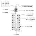
以上に対して、熱触媒体を用いたin-situクリーニング法が提案されている(特許文献1および特許文献2を参照)。本法は、金属からなる熱触媒体(発熱体)によってクリーニングガスを加熱・活性化させて、該活性化したガスと前記付着物とを反応・気化させて排気除去する、というものである。図11に本法を実現する装置の概略図を挙げる。600はクリーニングガスを噴出させるためのシャワーヘッド、601はクリーニングガスの導入口、602はクリーニングガスの噴出口、603はクリーニングガスが活性化されている活性ガス空間、604はクリーニングガスを加熱・活性化させるための熱触媒体、605は熱触媒体を加熱させるための加熱用電源、608はガスを排気するための真空ポンプである。なお本法の構成要件ではないが、図11中には、本装置を製膜装置として用いる場合の構成要件である基体(606)と基体加熱ヒーター(607)も示してある。
【0007】
ところで、本発明者らは、かねてからPECVD法とCat−CVD法とを融合させた新型CVD法の検討を進めており、既に、特許文献3〜6等において、Cat−PECVD法と命名した手法を開示してきた。図5に平行平板電極型のCat−PECVD法を実現する装置の概略図を、図6〜図10にはアンテナ電極型のCat−PECVD法を実現する装置の概略図を示す。
【0008】
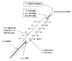
ここで、図5中の、700はシャワーヘッド、701は分子式にSiおよび/またはCを含むガスを含んだ原料系ガス導入口、702は分子式にSiとCを含まないガスからなる非Si非C系ガス導入口、703は原料系ガス導入経路、704は非Si非C系ガス導入経路、705は熱触媒体、706は加熱用電源、707はプラズマ空間、708はプラズマ生成用電極、709は高周波電源、710は原料系ガス噴出口、711は非Si・非C系ガス噴出口、712は被製膜用の基体、713は基体加熱用ヒーター、714はガス排気用真空ポンプ、715は輻射遮断部材である。
【0009】
また、図6は、アンテナ電極型Cat−PECVD法を実現する装置の一例を示す全体図であり、平板状の基体の製膜面が紙面に垂直方向に向いている場合に熱触媒体が内蔵されたアンテナ電極位置における断面図である。図7は管状のアンテナ電極をアレイ状に配置した一例を示すものであり、基体の製膜面が紙面に平行方向に向いている場合の断面図である(基体の存在を示すためにアレイ状アンテナ電極ユニットは一部のみ示してある。またアンテナ電極の端部構造の詳細は省略してある:詳細は図6や図8を参照)。図8は、熱触媒体を内蔵したアンテナ電極の詳細構造を示す断面図である。図9は、熱触媒体を内蔵したアンテナ電極の立体構造を示す斜視図である。図10は、2重管構造を有し熱触媒体を内蔵したアンテナ電極の断面図である。
【0010】
これら図6〜図10中の、101は分子式にSiとCを含まないガスからなる非Si非C系ガスの導入口、102は分子式にSiおよび/またはCを含むガスを含んだ原料系ガスの導入口、103は熱触媒体、104は熱触媒体103の加熱用電源、105は活性ガス空間、106aは熱触媒体を内蔵したアンテナ電極、106bは熱触媒体を内蔵しないアンテナ電極、107aおよび107bは高周波電源、108aおよび108cは位相変換器、108bおよび108dは電力分配器、109は被製膜用の基体、110は基体加熱用のヒーター、111aは熱触媒体内蔵アンテナ電極106aに設けられたガス噴出口(熱触媒体非内蔵アンテナ電極にも同じくガス噴出口が設けられているが説明は省略する)、112は電気絶縁用の絶縁部材、113は製膜空間を構成するチャンバー(製膜室)、114aおよび114bは、アンテナ電極内部に設けられた中空部、201はガス排出口である。なお、ガス排出口は真空ポンプに接続されているが、図示は省略する。
【0011】
以下、該Cat−PECVD法を図5に示した平行平板電極型のCat−PECVD装置をもとに説明するが、同様の原理説明は、図6〜図10に示したアンテナ電極型のCat−PECVD装置においてもあてはまることは言うまでもない。
【0012】
Cat−PECVD法は、例えば、原料系ガスとしてSiH4を、非Si非C系ガスとしてH2を用い、それぞれを製膜室に異なったガス導入経路にて分離導入し、H2はガス導入経路に設置された熱触媒体705によって加熱・活性化され、SiH4とはプラズマ空間707中で混合されることによってSi系膜の形成を行うものであって、高速製膜条件下であっても容易に結晶性の高い高品質結晶質Si膜を得ることができ、また同じく高速製膜条件化であっても光劣化の程度が少ない低水素濃度の高品質水素化アモルファスシリコン膜を得ることができるものである。これは、この方法では熱触媒体を用いることでH2の加熱・活性化量を、SiH4のプラズマによる分解・活性化量とは独立に自由に制御できること、またSiH4はプラズマのみによって活性化されるので、熱触媒体705による好ましくないラジカル生成を避けられること、また、輻射遮断部材715を設置することもできるので、熱触媒体705から基体712に直達する輻射を遮断でき製膜表面温度の好ましくない上昇を避けられること、さらには熱触媒体705によるガスヒーティング効果によって、気相中での高次シラン生成反応が抑制されること(SiH2分子の挿入反応による高次シラン生成反応は発熱反応であるため、ガスヒーティングによるガス温度の上昇は高次シラン生成反応に対してブレーキをかける効果を持つ)、などによるものと考えられる。
【0013】
なお、平行平板型電極に対するアンテナ電極型の利点は、VHFプラズマを用いても大面積均一製膜を実現しやすい点にある。
【0014】
さて、前記特許文献1および特許文献2に開示された熱触媒体を用いたin-situクリーニング法であるが、本法は本発明者らが開発した前記Cat−PECVD法に適用するには大きな問題点があることが判明した。
【0015】
すなわち、Cat−PECVD法においては、分離導入されるガスのうち非Si非C系ガスの導入経路中には熱触媒体が配設されており、理想的には該ガス導入経路にはSiやCを含む膜や粉体等の付着物は生成されないはずである。しかし実際には、例えば、前記したようにSiH4を原料ガスに用いる場合、製膜空間に投入された該SiH4や、該SiH4を母ガスとしてプラズマ空間の諸反応で生じたSiを含むガス分子が、僅かに前記非Si非C系ガス導入経路に拡散進入して該ガス導入経路に配設された熱触媒体によって加熱・活性化されることで、該ガス導入管中で前記付着物の生成がある程度は生じてしまう場合があるのであるが、前記した熱触媒体を用いたin-situクリーニング法では、熱触媒体がシャワーヘッド(従ってガス導入経路)の下流である製膜空間にしか配設されていないために、前記した非Si非C系ガス導入経路中で生成する付着物を容易には除去できないのである。
【0016】
さらに、このことは、当該製膜室を異導電型の膜を連続して製膜するような使い方を容易には許さないことを示していることは明白である。すなわち、目的の膜を製膜する前にそれまでの製膜履歴によって既に製膜室内面やガス導入経路内面に生成している付着物の有する導電型決定元素(ドーピング元素)が、目的とする膜の導電型の決定およびそのドーピングの程度、つまり膜品質に影響するからである。
【0017】
以上に対して、本発明者らは特許文献7において前記ガス導入経路に生成した付着物を除去するための方法を開示した。すなわち、クリーニングガスとしてH2を用い、該ガスを熱触媒体で加熱・活性化することで前記ガス導入経路内の付着物を除去するものである。このとき、製膜空間側の製膜室内壁のクリーニングについては、前記熱触媒体で活性化されたガスが、前記製膜空間において、さらにプラズマで追加活性されるので、通常のプラズマ単体での場合よりもクリーニングは促進される効果があった。
【0018】
しかしながら前記特許文献7においては、製膜空間側に存在するガスの活性化手段はプラズマに限定されていた。そのため、既に前記したプラズマを用いる場合の問題点(プラズマ生成位置が所定の位置に限定されるために、製膜空間全域に及ぶクリーニングが困難であること)は依然として解決できない状況に留まっていた。
【0019】
本発明は、このような背景のもとになされたものであり、優れて有効なガスクリーニング法を実現するCat−PECVD装置およびそれを実現する膜処理システムを提供することを目的とする。特に薄膜Si系太陽電池等に代表される光電変換装置におけるSi系薄膜の製膜において、装置メンテ作業の簡便化及び時間短縮、及び同一製膜室で異種導電型膜の製膜を連続して行えるようにすることで装置コストを大幅に低減させることを目的とする。
【0020】
【特許文献1】
特開2001−49436公報
【特許文献2】
特開2001−49437公報
【特許文献3】
特願2000−130858号
【特許文献4】
特願2001−293031号
【特許文献5】
特願2002−67445号
【特許文献6】
特願2002−155537号
【特許文献7】
特願2002−007147号
【0021】
【課題を解決するための手段】
本発明のCat−PECVD装置は、分子式にSiおよび/またはCを含むガスを含んだ原料系ガスと、ガス導入経路に配設された第1の熱触媒体によって加熱される分子式にSiとCを含まないガスからなる非Si非C系ガスとが、それぞれ分離された状態で、製膜空間に設置されたプラズマ生成電極を兼ねるシャワーヘッドに設けられた複数のガス噴出口から前記製膜空間に噴出され、該製膜空間に噴出されて混合したガスは、高周波電源に接続された前記シャワーヘッドによって生成されたプラズマによって分解・活性化されて、前記製膜空間において前記シャワーヘッドに対向して配置された基体に膜が堆積されるように成したCat−PECVD装置であって、前記非Si非C系ガス導入経路に配設された熱触媒体とは別の第2の熱触媒体が前記製膜空間に配設されており、水素ガス、分子式にフッ素(F)を含んだガス、あるいは分子式に塩素(Cl)を含んだガスのうち、少なくともいずれかを含んだクリーニング用ガスが、少なくとも前記非Si非C系ガス導入経路を通して前記製膜空間に導入され、前記第1の熱触媒体及び第2の熱触媒体によって加熱・活性化され、該加熱・活性化されたガスによって前記製膜空間を構成する製膜室内に堆積した付着物をエッチング除去するクリーニング機構を備えており、前記第2の熱触媒体は、製膜時に前記付着物の被付着対象物とならないようにクリーニング時と異なる位置に待避されることを特徴とする。
【0022】
また、分子式にSiおよび/またはCを含むガスを含んだ原料系ガスと、ガス導入経路に配設された第1の熱触媒体によって加熱される分子式にSiとCを含まないガスからなる非Si非C系ガスとが、それぞれ分離された状態で、製膜空間に設置された中空構造を有したアンテナ電極の中空部を通って該アンテナ電極に設けられた複数のガス噴出口から前記製膜空間に噴出され、該製膜空間に噴出されて混合したガスは、高周波電源に接続された前記アンテナ電極によって生成されたプラズマによって分解・活性化されて、前記製膜空間において前記アンテナ電極に対向して配置された基体に膜が堆積されるように成したCat−PECVD装置であって、前記非Si非C系ガス導入経路に配設された熱触媒体とは別の第2の熱触媒体が前記製膜空間に配設されており、水素ガス、分子式にフッ素(F)を含んだガス、あるいは分子式に塩素(Cl)を含んだガスのうち、少なくともいずれかを含んだクリーニング用ガスが、少なくとも前記非Si非C系ガス導入経路を通して前記製膜空間に導入され、前記第1の熱触媒体及び第2の熱触媒体によって加熱・活性化され、該加熱・活性化されたガスによって前記製膜空間を構成する製膜室内に堆積した付着物をエッチング除去するクリーニング機構を備えており、前記第2の熱触媒体は、製膜時に前記付着物の被付着対象物とならないようにクリーニング時と異なる位置に待避されることを特徴とする。
【0024】
また、本発明の膜処理システムは、上記のCat−PECVD装置から成る製膜室を少なくとも一室含む複数の真空室からなる膜処理システムであって、前記製膜室は、Si系膜またはC系膜をp型化できるドーピングガス、あるいはn型化できるドーピングガスのうち、少なくとも一方を導入できる構造を有していることを特徴とする。
【0025】
また、上記膜処理システムであって、p型膜、実質的にi型膜、およびn型膜のうち、少なくとも導電型の異なる2種以上の膜を積層したSi系膜またはC系膜を製膜するにあたって、少なくともi型膜を製膜する直前には、クリーニングガスによって製膜室内をクリーニングすることを特徴とする。
【0026】
さらに、この膜処理システムは、真空弁によって隔離され基体を格納できる待避室が隣接して設けられていることを特徴とする
【0027】
【発明の実施の形態】
以下、本発明の実施形態を模式的に図示した図面に基づいて詳細に説明する。
【0028】
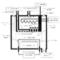
図1は、平行平板電極型のCat−PECVD法を実現する装置の一例を示す全体図である。ここで、705aは非Si非C系ガス導入経路に配設された第1の熱触媒体、705bは製膜空間に配設された第2の熱触媒体、706aは第1の熱触媒体用の加熱用電源、706bは第2の熱触媒体用の加熱用電源であり、それ以外の番号は図5のそれと同一にとってある。
【0029】
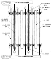
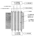
また、図2は、アンテナ電極型のCat−PECVD法を実現する装置の一例を示す全体図であり、平板状の基体の製膜面が紙面に垂直方向に向いている場合に熱触媒体が内蔵されたアンテナ電極位置における断面図である。図3は、アレイ状アンテナ電極をその中心軸方向から見た断面図である。
【0030】
これら図中の、103aは非Si非C系ガス導入経路に配設された第1の熱触媒体、103bは製膜空間に配設された第2の熱触媒体、104aは第1の熱触媒体用の加熱用電源、104bは第2の熱触媒体用の加熱用電源、109a及び109bは基体、111bは熱触媒体非内蔵アンテナ電極106bに設けられたガス噴出口であり、それ以外の番号は、図6のそれと同一にとってある。
【0031】
なお、以下では主に図1に示された平行平板型Cat−PECVD装置を例にとって説明していくが、同様の説明は図2及び図3に示されたアンテナ電極型Cat−PECVD装置にも適用できるので、特に個別の説明を必要とする部分以外は説明を省略する。
【0032】
さて、図1に示されたCat−PECVD装置を用いて、例えば、原料系ガスとしてSiH4を、また非Si非C系ガスとしてH2を用いて、Si系膜を基体に製膜した場合を例にとって以下説明する。
【0033】
Si系膜を基体に製膜すると、不可避的に基体以外の製膜室内にSi系の膜や粉体などが付着する。また、Cat−PECVD法においては、製膜モードでは第1の熱触媒体705aを加熱状態とするので、製膜条件によっては、既に従来技術およびその課題の欄で述べたように、非Si非C系ガス導入経路の熱触媒体近傍にも前記付着物が生成することがある。
【0034】
これら付着物は前記基体上に製膜されるSi系膜の品質に大きな影響を及ぼす。すなわち、付着物である膜の剥離によって生じたゴミや、粉体の脱離や、付着物が活性ガスと反応して生じる高次シラン系ガスなどが前記Si系膜に取り込まれることによって膜品質は低下する。
【0035】
そこで、これら付着物を、少なくとも1回以上の製膜モードを経た後に、ガスクリーニングモードに移行して除去し、付着物の存在が基体上に製膜される所望の膜の品質に悪影響を及ぼす程度を低減する。ガスクリーニング用のクリーニングガスは、少なくとも非Si非C系ガス導入経路から導入し、第1の熱触媒体705aおよび第2の熱触媒体705bで加熱・活性化させる。該活性化されたクリーニングガスは、非Si非C系ガス導入経路上の付着物および製膜空間内の付着物と反応して、付着物は気化・排気されクリーニングが進行する。
【0036】
ここで、クリーニングガスとしては、水素(H2)、分子式にフッ素(F)を含んだガス、あるいは分子式に塩素(Cl)を含んだガスのうち、少なくともいずれかを含んだガスを用いることができる。分子式にフッ素を含んだガス、および分子式に塩素を含んだガスとしては、SF6、NF3、CF4、C2F6、C3F8、CCl4、C2ClF5、ClF3、CClF3、などを用いることができる。
【0037】
ここで、熱触媒体705a及び705bは、これに電流を流してそのジュール発熱で加熱・高温化させて熱触媒体として機能させるために、少なくともその表面が金属材料からなるが、この金属材料はより好ましくは高融点金属材料であるTa、W、Re、Os、Ir、Nb、Mo、Ru、Ptのうちの少なくとも1種を主成分とするような金属材料からなることが望ましい。また、熱触媒体の形状としては、通常、上記のような金属材料をワイヤ状にしたものを用いることが多いが、特にワイヤ状に限るものではなく、板状、メッシュ状のものも用いることができる。なお、熱触媒体材料たる金属材料中に膜形成にあたって好ましくない不純物が含まれている場合には、熱触媒体705a及び705bを製膜に使用する前に、予め製膜時の加熱温度以上の温度で数分間以上予備加熱すれば、不純物低減に効果的である。
【0038】
なお、熱触媒体705a及び705bの加熱用電源706a及び706bとしては、通常、直流電源を用いるのが簡便であるが、プラズマを生成させない程度の低周波の交流電源を用いても支障はない。
【0039】
また、熱触媒体の温度は、用いるクリーニングガス種によって異なる。例えばH2のように熱触媒体をエッチングすることはないクリーニングガスにおいては、1000℃以上とする。圧力にもよるがH2の原子状水素Hへの分解反応はおよそ1000℃程度以上から顕著になってき、その分解の程度に応じてクリーニング効果も増大するからである。一方、Fを含んだガスやClを含んだガスをクリーニングガスに用いる場合には、熱触媒体の温度が充分に高くない場合、熱触媒体自体がこれらクリーニングガスとの反応によってエッチング消耗されてしまう場合がある。この場合は、熱触媒体の温度を、熱触媒体材料とこれらクリーニングガスとの反応が進行する前にこれらクリーニングガスあるいはその分解成分が熱触媒体表面から熱脱離するような温度にまで高めてやればよい。なお、熱触媒体の温度は、熱触媒体材料の蒸発が問題にならない程度以下にしなければならない。この最高使用温度は熱触媒体の材料によって異なるが、その材料の融点温度よりも500〜1000℃程度低い温度をおよその目安とすることができる。
【0040】
ここで、製膜空間に配設された第2の熱触媒体705bは、装置を製膜モード(このとき第2の熱触媒体は加熱されていない)で使用している間は、ガスクリーニングモード時の製膜空間での配設位置とは異なる位置に配設できるようにしておく。これは、製膜モードにおいては該第2の熱触媒体がこれまでに述べた付着物の被付着対象物となり、これまでに述べてきた問題を惹起するからである。具体的には、図1において、第2の熱触媒体705bを、装置が製膜モードに入る前に、予め下方向に移動させてヒーター部品に設けられた溝(不図示)などに埋め込まれるように待避させておく。こうしておけば、製膜は第2の熱触媒体705bがあたかも存在しない場合と同様の条件で実現することができ、前記問題を回避できる。なお、第2の熱触媒体の待避方法は上記方法に限るものではなく、例えば水平方向に待避させてもよいのは言うまでもない。
【0041】
なお、図2と図3には、アンテナ電極型Cat−PECVD法においての第2の熱触媒体103bの配設方法の一例を示してあるが、この場合も製膜モードにおいては図示したガスクリーニングモードでの配設位置とは異なる位置に配設する。上記と同等の理由からである。
<異種導電型の半導体膜を同じ製膜室で製膜できる膜処理システムとプロセス>
図12には、i型の水素化アモルファスシリコン膜を光活性層に用いたp−i−n型セル(トップセル)と、i型の微結晶シリコン膜を光活性層に用いたp−i−n型セル(ボトムセル)とを積層したタンデム型薄膜Si太陽電池を製造するための従来装置の一例を示してある。ここではi型の水素化アモルファスシリコン膜形成とi型の微結晶シリコン膜の形成にCat−PECVD法を利用する例を示してあるが、もちろん、他の膜(p型膜、n型膜)の形成にもCat−PECVD法を用いても構わない。
【0042】
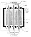
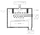
ここで、本発明のガスクリーニング法を適用した場合の装置構成の一例を図4に示す。ここでは、前記p−i−n型トップセルを1つの製膜室で、同じく前記p−i−n型ボトムセルを1つの製膜室で実現する場合の例を示してある。それぞれの製膜室にはp型膜及びn型膜も形成できるように、B 2 H 6 に代表されるp型ドーピングガス及びPH 3 に代表されるn型ドーピングガスを導入できるようにしてある。このように、従来は図12に示したように、p型膜、i型膜、n型膜をそれぞれ独立した製膜室で形成していたのに対して、本発明のガスクリーニング法によれば、ガスクリーニングによってそれまでに堆積した製膜室内の付着物を除去できるので(すなわちそれまでの製膜履歴を消去できるので)、同一製膜室であっても異種導電型の膜を連続製膜できるのである。
【0043】
また、ガスクリーニングは、少なくともi型膜を形成する場合には、その製膜直前に実施する。これはi型膜の品質が太陽電池の特性を決定づけるからである。一方、p型膜及びn型膜形成の場合には、その製膜直前に、ガスクリーニングを必ずしも実施する必要はない。これは、通常、太陽電池用のp型膜及びn型膜のドーピング濃度は、製膜室のそれまでの製膜履歴に影響される程低いものではなく、充分高い場合がほとんどだからである。しかしできうれば実施するのが望ましいことは言うまでもない。
【0044】
なお、ガスクリーニング法による異種導電型膜の連続形成自体は従来から知られていた技術であるが、Cat−PECVD法を用いた製膜法を用いる場合においては、本発明のガスクリーニング法(製膜室内だけではなく、非Si非C系ガス導入経路もガスクリーニングする方法)が必須であるのは明らかである。
【0045】
また、図4には、製膜室をガスクリーニングするときに、基体を一時待避させておく待避室も示してある。これによってガスクリーニングの影響が基体に及ぶことを避けることができる。
【0046】
また、上記では1つの製膜室で、p型、i型、n型の3種の膜を製膜する場合について述べたが、もちろん、これらのうちの2種の膜、あるいは1種の膜を製膜する場合にも本法は適用可能であることは言うまでもない。
【0047】
【発明の効果】
以上、本発明のCat−PECVD装置およびそれを用いた膜処理システムによれば、優れて有効なガスクリーニング法及びそれを実現する装置構成を提供することができるので、装置メンテ作業の簡便化及び大幅な時間短縮を実現することができる。
【0048】
また、同一製膜室で異種導電型膜の製膜を連続して行えるようになるため装置コストも大幅に抑えることができる。
【図面の簡単な説明】
【図1】本発明に係るガスクリーニング法を実現する装置の一例を模式的に説明する断面図である。
【図2】本発明に係るガスクリーニング法を実現する装置の一例を模式的に説明する断面図である。
【図3】本発明に係るガスクリーニング法を実現する装置構成の一例を模式的に説明する図であり、アンテナ電極の中心軸方向からみた断面図である。
【図4】本発明に係るCat−PECVD法を実現する膜処理システムの一例を説明する図である。
【図5】従来のCat−PECVD装置の一例を模式的に説明する図である。
【図6】従来のCat−PECVD装置の一例を模式的に説明する図である。
【図7】従来のCat−PECVD装置の構成の一例を模式的に説明する図である。
【図8】従来のCat−PECVD装置の部品の一例を模式的に説明する断面図である。
【図9】従来のCat−PECVD装置の部品の一例を模式的に説明する斜視図である。
【図10】従来のCat−PECVD装置の部品の一例を模式的に説明する断面図である。
【図11】従来のガスクリーニング方法を実現する装置の一例を模式的に説明する断面図である。
【図12】従来の膜処理システムの一例を説明する模式図である。
【符号の説明】
103a:非Si非C系ガス導入経路に配設された第1の熱触媒体
101:分子式にSiとCを含まないガスからなる非Si非C系ガスの導入口
102:分子式にSiおよび/またはCを含むガスを含んだ原料系ガスの導入口
103:熱触媒体
103b:製膜空間に配設された第2の熱触媒体
104:熱触媒体103の加熱用電源
104a:第1の熱触媒体用の加熱用電源
104b:第2の熱触媒体用の加熱用電源
105:活性ガス空間
106a:熱触媒体を内蔵したアンテナ電極
106b:熱触媒体を内蔵しないアンテナ電極
107a、107b:高周波電源
108a、108c:位相変換器
108b、108d:電力分配器
109:被製膜用の基体
109a、109b:基体
110:基体加熱用のヒーター
111b:熱触媒体非内蔵アンテナ電極
111a:熱触媒体内蔵アンテナ電極106aに設けられたガス噴出口
112:電気絶縁用の絶縁部材
113:製膜空間を構成するチャンバー(製膜室)
114a、114b:アンテナ電極内部に設けられた中空部
201:ガス排出口
700:シャワーヘッド
701:分子式にSiおよび/またはCを含むガスを含んだ原料系ガス導入口
702:分子式にSiとCを含まないガスからなる非Si非C系ガス導入口
703:原料系ガス導入経路
704:非Si非C系ガス導入経路
705:熱触媒体
705a:非Si非C系ガス導入経路に配設された第1の熱触媒体
705b:製膜空間に配設された第2の熱触媒体
706:加熱用電源
706a:第1の熱触媒体用の加熱用電源
706b:第2の熱触媒体用の加熱用電源
707:プラズマ空間
708:プラズマ生成用電極
709:高周波電源
710:原料系ガス噴出口
711:非Si・非C系ガス噴出口
712:被製膜用の基体
713:基体加熱用ヒーター
714:ガス排気用真空ポンプ
715:輻射遮断部材[0001]
BACKGROUND OF THE INVENTION
The present invention relates to PECVD (Plasma Enhanced Chemical Vapor Deposition), which is a CVD (Chemical Vapor Deposition) method using plasma as a means for decomposing and activating a film forming gas, and decomposition and heating of a film forming gas.・ New CVD that combines Cat-CVD (Catalytic Chemical Vapor Deposition: catalytic CVD) method (same principle as HW-CVD (hot wire CVD) method), which is a CVD method using a thermal catalyst as the activation means The present invention relates to a Cat-PECVD apparatus and a film processing system using the Cat-PECVD apparatus.
[0002]
[Prior art and its problems]
In thin film formation using a vacuum apparatus, it is usually difficult to limit thin film formation to only a desired substrate, and inevitably film, powder, etc. adhere to the film formation chamber other than the desired substrate. To do. Since these deposits act as a contamination source in various meanings such as an impurity contamination source and a foreign matter contamination source for film formation on a desired substrate, in the thin film deposition apparatus, Periodic removal (cleaning) is essential.
[0003]
The usual cleaning method is to open the apparatus to the atmosphere and clean the inner wall of the film formation and the internal components using mechanical means such as wiping or scraping, or chemical means such as an etching solution. However, this method requires a very long time for evacuation after cleaning in order to release the apparatus to the atmosphere, and also requires a lot of time and effort for cleaning itself, so that the productivity of the apparatus is remarkably reduced. In particular, in a product with a very large production amount, such as a thin-film Si-based solar cell, and therefore in a thin-film deposition apparatus in which a large amount of thin-film deposition is performed in a short time, the method is a fatal decrease in productivity, that is, a significant reduction. Will result in a significant cost increase.
[0004]
On the other hand, there is known a method (in-situ cleaning) in which cleaning of the inside of the apparatus is performed in a simple and short time while maintaining a vacuum state by flowing a cleaning gas without opening the apparatus to the atmosphere. A typical method is to decompose and activate a gas containing fluorine (F) or chlorine (Cl) in a cleaning gas by plasma, and react the activated gas with the deposits to vaporize and exhaust the gas. That's it. However, normally, plasma cannot be generated in the entire area of the apparatus, and the plasma generation region is limited to a part of the apparatus, so that there is a problem that the removal of the deposits is insufficient.
[0005]
In contrast, ClFThreeAlso known is an in-situ cleaning method that uses a gas with high reactivity such as raising the temperature in the film forming chamber to a predetermined temperature and reacting and vaporizing the reactive gas and deposits to remove the exhaust gas. It has been. This compensates for the drawbacks of the method using plasma as long as the temperature in the entire film forming chamber can be raised to a predetermined temperature, but usually the temperature in the film forming chamber needs to be about 200 ° C. For this reason, there are problems such as a considerable thermal load on the apparatus, a temperature rising process until cleaning, and a temperature lowering process after cleaning which requires a considerable time (see Patent Document 1).
[0006]
In contrast, an in-situ cleaning method using a thermal catalyst has been proposed (see Patent Document 1 and Patent Document 2). In this method, a cleaning gas is heated and activated by a thermal catalyst body (heating element) made of metal, and the activated gas and the deposits are reacted and vaporized for exhaust removal. FIG. 11 shows a schematic diagram of an apparatus for realizing the present method. 600 is a shower head for jetting cleaning gas, 601 is a cleaning gas introduction port, 602 is a cleaning gas jet port, 603 is an active gas space in which the cleaning gas is activated, 604 is heating and activation of the cleaning gas 605 is a heating power source for heating the thermal catalyst body, and 608 is a vacuum pump for exhausting the gas. Although not a constituent requirement of the present method, FIG. 11 also shows a base (606) and a base heater (607) that are constituent requirements when the apparatus is used as a film forming apparatus.
[0007]
By the way, the present inventors have been studying a new type of CVD method in which PECVD method and Cat-CVD method have been fused for some time, and a method named Cat-PECVD method has already been named in Patent Documents 3-6. Has been disclosed. FIG. 5 is a schematic view of an apparatus for realizing a parallel plate electrode type Cat-PECVD method, and FIGS. 6 to 10 are schematic views of an apparatus for realizing an antenna electrode type Cat-PECVD method.
[0008]
Here, in FIG. 5, 700 is a shower head, 701 is a raw material gas inlet containing a gas containing Si and / or C in the molecular formula, and 702 is a non-Si non-Si composed of a gas not containing Si and C in the molecular formula. C gas introduction port, 703 is a raw material gas introduction path, 704 is a non-Si non-C gas introduction path, 705 is a thermal catalyst, 706 is a heating power source, 707 is a plasma space, 708 is a plasma generation electrode, 709 Is a high-frequency power source, 710 is a raw material gas outlet, 711 is a non-Si / non-C gas outlet, 712 is a substrate for film formation, 713 is a heater for heating the substrate, 714 is a vacuum pump for exhausting gas, and 715 is It is a radiation blocking member.
[0009]
FIG. 6 is an overall view showing an example of an apparatus for realizing the antenna electrode type Cat-PECVD method. When the film-forming surface of the flat substrate is oriented in a direction perpendicular to the paper surface, a thermal catalyst is incorporated. It is sectional drawing in the antenna electrode position made. FIG. 7 shows an example in which the tubular antenna electrodes are arranged in an array, and is a cross-sectional view when the film-forming surface of the substrate faces in a direction parallel to the paper surface (in order to show the presence of the substrate, an array shape). Only a part of the antenna electrode unit is shown, and details of the end structure of the antenna electrode are omitted: see FIG. 6 and FIG. 8 for details). FIG. 8 is a cross-sectional view showing a detailed structure of an antenna electrode incorporating a thermal catalyst. FIG. 9 is a perspective view showing a three-dimensional structure of an antenna electrode incorporating a thermal catalyst. FIG. 10 is a cross-sectional view of an antenna electrode having a double tube structure and incorporating a thermal catalyst.
[0010]
6 to 10, 101 is a non-Si non-C gas introduction port made of a gas not containing Si and C in the molecular formula, and 102 is a raw material gas containing a gas containing Si and / or C in the molecular formula. , 103 is a thermal catalyst, 104 is a power source for heating the thermal catalyst 103, 105 is an active gas space, 106a is an antenna electrode with a built-in thermal catalyst, 106b is an antenna with no built-in thermal catalyst, 107a And 107b are high-frequency power supplies, 108a and 108c are phase converters, 108b and 108d are power distributors, 109 is a substrate for film formation, 110 is a heater for heating the substrate, and 111a is provided on the
[0011]
Hereinafter, the Cat-PECVD method will be described based on the parallel plate electrode-type Cat-PECVD apparatus shown in FIG. 5, but the same principle will be described for the antenna electrode-type Cat− shown in FIGS. 6 to 10. Needless to say, this also applies to the PECVD apparatus.
[0012]
The Cat-PECVD method uses, for example, SiH as a raw material gas.FourH as non-Si non-C based gas2Are separated and introduced into the film forming chamber through different gas introduction paths, and H2Is heated and activated by the thermal catalyst 705 installed in the gas introduction path, and SiHFourIs to form a Si-based film by mixing in the
[0013]
The advantage of the antenna electrode type over the parallel plate type electrode is that a large-area uniform film formation can be easily realized even using VHF plasma.
[0014]
Now, the in-situ cleaning method using the thermal catalyst disclosed in Patent Document 1 and
[0015]
That is, in the Cat-PECVD method, a thermal catalyst is disposed in the introduction path of the non-Si non-C gas among the gases to be separated and introduced, and ideally, Si or Deposits such as C-containing films and powders should not be generated. However, in practice, for example, as described above, SiHFourWhen Si is used as the source gas, the SiH introduced into the film forming spaceFourAnd the SiHFourThe gas molecules containing Si generated by various reactions in the plasma space using the gas as a base gas are slightly diffused and entered into the non-Si non-C gas introduction path and heated by the thermal catalyst disposed in the gas introduction path. When activated, the deposit may be generated to some extent in the gas introduction pipe. However, in the in-situ cleaning method using the thermal catalyst, the thermal catalyst is Since the film is disposed only in the film forming space downstream of the shower head (and therefore the gas introduction path), the deposits generated in the non-Si non-C gas introduction path cannot be easily removed.
[0016]
Furthermore, this clearly shows that the film forming chamber is not easily allowed to be used for continuously forming films of different conductivity types. That is, the conductive type determining element (doping element) of the deposit already generated on the inner surface of the film forming chamber and the inner surface of the gas introduction path based on the film forming history until the target film is formed is the target. This is because it determines the conductivity type of the film and the degree of doping, that is, the film quality.
[0017]
In contrast, the present inventors disclosed a method for removing deposits generated in the gas introduction path in
[0018]
However, in
[0019]
The present invention has been made based on such a background, and an object thereof is to provide a Cat-PECVD apparatus that realizes an excellent and effective gas cleaning method and a film processing system that realizes the Cat-PECVD apparatus. In particular, in the formation of Si-based thin films in photoelectric conversion devices typified by thin-film Si-based solar cells, etc., device maintenance work is simplified and time is reduced, and different conductivity type films are continuously formed in the same film-forming chamber. The purpose is to greatly reduce the cost of the apparatus by making it possible.
[0020]
[Patent Document 1]
JP 2001-49436 A
[Patent Document 2]
JP 2001-49437 A
[Patent Document 3]
Japanese Patent Application No. 2000-130858
[Patent Document 4]
Japanese Patent Application No. 2001-293031
[Patent Document 5]
Japanese Patent Application No. 2002-67445
[Patent Document 6]
Japanese Patent Application No. 2002-155537
[Patent Document 7]
Japanese Patent Application No. 2002-007147
[0021]
[Means for Solving the Problems]
The Cat-PECVD apparatus according to the present invention includes a raw material gas containing a gas containing Si and / or C in the molecular formula, and Si and C in the molecular formula heated by the first thermal catalyst disposed in the gas introduction path. The film-forming space is formed from a plurality of gas outlets provided in a shower head that also serves as a plasma generation electrode installed in the film-forming space in a state where the non-Si non-C gas composed of a gas that does not contain gas is separated from each other. The gas mixed into the film forming space is decomposed and activated by the plasma generated by the shower head connected to a high-frequency power source, and faces the shower head in the film forming space. A Cat-PECVD apparatus configured to deposit a film on a substrate disposed in a second position, wherein the second is different from the thermal catalyst disposed in the non-Si non-C gas introduction path. A catalyst body is disposed in the film forming space, and for cleaning containing at least one of hydrogen gas, gas containing fluorine (F) in molecular formula, or gas containing chlorine (Cl) in molecular formula A gas is introduced into the film forming space through at least the non-Si non-C gas introduction path, heated and activated by the first thermal catalyst body and the second thermal catalyst body, and heated and activated. A cleaning mechanism is provided for etching and removing deposits deposited in the film forming chamber constituting the film forming space by gas.The second thermal catalyst is retracted at a position different from that at the time of cleaning so as not to become an object to be adhered to when the film is formed.It is characterized by that.
[0022]
In addition, a non-chemical gas consisting of a raw material gas containing a gas containing Si and / or C in the molecular formula and a gas not containing Si and C in the molecular formula heated by the first thermal catalyst disposed in the gas introduction path. The Si non-C gas is separated from each other through a plurality of gas outlets provided in the antenna electrode through a hollow portion of the antenna electrode having a hollow structure installed in the film forming space. The gas injected into the film space and mixed into the film forming space is decomposed and activated by the plasma generated by the antenna electrode connected to a high-frequency power source, and is then applied to the antenna electrode in the film forming space. A Cat-PECVD apparatus configured to deposit a film on a substrate disposed oppositely, wherein the second heat is different from the thermal catalyst disposed in the non-Si non-C gas introduction path. The catalyst body is in front At least a cleaning gas containing at least one of hydrogen gas, gas containing fluorine (F) in the molecular formula, or gas containing chlorine (Cl) in the molecular formula is disposed in the film forming space. It is introduced into the film forming space through the non-Si non-C based gas introduction path, heated and activated by the first thermal catalyst body and the second thermal catalyst body, and the production is performed by the heated and activated gas. Equipped with a cleaning mechanism that removes deposits deposited in the deposition chamber that forms the membrane space.The second thermal catalyst is retracted at a position different from that at the time of cleaning so as not to become an object to be adhered to when the film is formed.It is characterized by that.
[0024]
The film processing system of the present invention is a film processing system comprising a plurality of vacuum chambers including at least one film forming chamber comprising the above Cat-PECVD apparatus, wherein the film forming chamber comprises an Si-based film or C It has a structure in which at least one of a doping gas that can make the system film p-type or a doping gas that can make it n-type can be introduced.
[0025]
Further, in the film processing system, an Si-based film or a C-based film in which at least two kinds of films having different conductivity types are stacked among a p-type film, a substantially i-type film, and an n-type film is manufactured. In forming the film, at least immediately before forming the i-type film, the film forming chamber is cleaned with a cleaning gas.
[0026]
Further, this membrane processing system is characterized in that a waiting room is provided adjacent to the substrate, which is isolated by a vacuum valve and can store a substrate.
[0027]
DETAILED DESCRIPTION OF THE INVENTION
Embodiments of the present invention will be described below in detail with reference to the drawings schematically shown.
[0028]
FIG. 1 is an overall view showing an example of an apparatus for realizing a parallel plate electrode type Cat-PECVD method. Here, 705a is a first thermal catalyst disposed in the non-Si non-C gas introduction path, 705b is a second thermal catalyst disposed in the film forming space, and 706a is a first thermal catalyst. A heating power source 706b is a heating power source for the second thermal catalyst, and the other numbers are the same as those in FIG.
[0029]
FIG. 2 is an overall view showing an example of an apparatus for realizing the antenna electrode type Cat-PECVD method. When the film-forming surface of the flat substrate is oriented in a direction perpendicular to the paper surface, the thermal catalyst is It is sectional drawing in the position of the built-in antenna electrode. FIG. 3 is a cross-sectional view of the arrayed antenna electrode as viewed from the central axis direction.
[0030]
In these drawings, 103a is a first thermal catalyst disposed in the non-Si non-C gas introduction path, 103b is a second thermal catalyst disposed in the film forming space, and 104a is the first heat catalyst. A heating power source for the catalyst body, 104b is a heating power source for the second thermal catalyst body, 109a and 109b are bases, 111b is a gas outlet provided in the antenna electrode 106b without the built-in thermal catalyst body, and the others Is the same as that of FIG.
[0031]
In the following description, the parallel plate Cat-PECVD apparatus shown in FIG. 1 will be mainly described as an example, but the same description applies to the antenna electrode Cat-PECVD apparatus shown in FIGS. Since it can be applied, the description will be omitted except for parts that require individual explanation.
[0032]
Now, using the Cat-PECVD apparatus shown in FIG.FourAnd H as non-Si non-C gas2An example in which a Si-based film is formed on a substrate using a film will be described below.
[0033]
When a Si-based film is formed on a substrate, inevitably, a Si-based film or powder adheres to a film forming chamber other than the substrate. Further, in the Cat-PECVD method, the first thermal catalyst 705a is heated in the film forming mode. Therefore, depending on the film forming conditions, as described above in the section of the related art and the problem, non-Si non-Si The deposit may also be generated in the vicinity of the thermal catalyst in the C-based gas introduction path.
[0034]
These deposits greatly affect the quality of the Si-based film formed on the substrate. That is, film quality is obtained by taking in the Si-based film such as dust generated by peeling of the film that is a deposit, desorption of powder, and higher silane gas generated by the reaction of the deposit with the active gas. Will decline.
[0035]
Therefore, after these deposits have passed through the film forming mode at least once, they are put into the gas cleaning mode.MigrationTo reduce the extent to which the presence of deposits adversely affects the quality of the desired film deposited on the substrate. A cleaning gas for gas cleaning is introduced at least from the non-Si non-C gas introduction path, and is heated and activated by the first thermal catalyst body 705a and the second thermal catalyst body 705b. The activated cleaning gas reacts with the deposit on the non-Si non-C gas introduction path and the deposit in the film forming space, the deposit is vaporized and exhausted, and cleaning proceeds.
[0036]
Here, as the cleaning gas, hydrogen (H2), A gas containing fluorine (F) in the molecular formula, or a gas containing at least one of chlorine (Cl) in the molecular formula can be used. The gas containing fluorine in the molecular formula and the gas containing chlorine in the molecular formula include SF6, NFThree, CFFour, C2F6, CThreeF8, CClFour, C2ClFFive, ClFThree, CClFThree, Etc. can be used.
[0037]
Here, the thermal catalyst bodies 705a and 705b are made of a metal material at least on the surface in order to function as a thermal catalyst body by passing an electric current therethrough and heating and raising the temperature by Joule heat generation. More preferably, it is made of a metal material containing as a main component at least one of Ta, W, Re, Os, Ir, Nb, Mo, Ru, and Pt, which are refractory metal materials. In addition, as the shape of the thermal catalyst, a metal material as described above is usually used in the form of a wire. However, the shape is not particularly limited to a wire shape, and a plate-like or mesh-like shape is also used. Can do. In addition, when the metal material which is a thermal catalyst body material includes an undesirable impurity for film formation, before using the thermal catalyst bodies 705a and 705b for the film formation, the heating temperature at the time of film formation or higher is previously set. Preheating at temperature for several minutes or more is effective in reducing impurities.
[0038]
As the heating power supplies 706a and 706b for the thermal catalyst bodies 705a and 705b, it is usually easy to use a DC power supply, but there is no problem even if a low-frequency AC power supply that does not generate plasma is used.
[0039]
The temperature of the thermal catalyst varies depending on the type of cleaning gas used. For example, H2In the case of the cleaning gas that does not etch the thermal catalyst as described above, the temperature is set to 1000 ° C. or higher. H depending on pressure2This is because the decomposition reaction of
[0040]
Here, the second thermal catalyst body 705b disposed in the film forming space is used for gas cleaning while the apparatus is being used in the film forming mode (the second thermal catalyst body is not heated at this time). So that it can be placed at a position different from the position in the film-forming space during mode.deep. This is because in the film forming mode, the second thermal catalyst is an object to be adhered to the deposits described so far and causes the problems described so far. Specifically, in FIG. 1, the second thermal catalyst 705 b is moved downward in advance and embedded in a groove (not shown) provided in the heater component before the apparatus enters the film forming mode. Let's save. In this way, the film formation can be realized under the same conditions as when the second thermal catalyst 705b does not exist, and the above problem can be avoided. Note that the method for retracting the second thermal catalyst is not limited to the above method, and it is needless to say that the second thermal catalyst may be retracted in the horizontal direction, for example.
[0041]
2 and 3 show an example of a method for disposing the second thermal catalyst 103b in the antenna electrode type Cat-PECVD method. In this case as well, the gas cleaning shown in FIG. Arranged at a position different from the arrangement position in the modeTo do.For the same reason as aboveIs.
<Film treatment system and process capable of depositing different conductivity type semiconductor films in the same deposition chamber>
FIG. 12 shows a p-i-n type cell (top cell) using an i-type hydrogenated amorphous silicon film as a photoactive layer, and a p-i using an i-type microcrystalline silicon film as a photoactive layer. An example of a conventional apparatus for manufacturing a tandem-type thin-film Si solar cell in which an n-type cell (bottom cell) is stacked is shown. In this example, the Cat-PECVD method is used to form an i-type hydrogenated amorphous silicon film and an i-type microcrystalline silicon film. Of course, other films (p-type film, n-type film) are used. The Cat-PECVD method may be used for forming the film.
[0042]
Here, FIG. 4 shows an example of an apparatus configuration when the gas cleaning method of the present invention is applied. Here, an example is shown in which the p-i-n type top cell is realized by one film-forming chamber and the p-i-n type bottom cell is realized by one film-forming chamber. In order to form a p-type film and an n-type film in each film forming chamber, 2 H 6 P-type doping gas and PH represented by 3 An n-type doping gas typified by can be introduced. Thus, as shown in FIG. 12, the p-type film, the i-type film, and the n-type film are conventionally formed in independent film forming chambers, but according to the gas cleaning method of the present invention. For example, since the deposits deposited in the film forming chamber can be removed by gas cleaning (that is, the previous film forming history can be erased), different types of conductive films can be continuously manufactured even in the same film forming chamber. A film can be formed.
[0043]
Further, the gas cleaning is performed immediately before the film formation when at least the i-type film is formed. This is because the quality of the i-type film determines the characteristics of the solar cell. On the other hand, in the case of forming a p-type film and an n-type film, it is not always necessary to perform gas cleaning immediately before the film formation. This is because the doping concentration of the p-type film and the n-type film for solar cells is usually not high enough to be influenced by the film forming history of the film forming chamber, and is often sufficiently high. However, it goes without saying that it is desirable to implement it if possible.
[0044]
The continuous formation of the different conductivity type films by the gas cleaning method is a conventionally known technique. However, when the film forming method using the Cat-PECVD method is used, the gas cleaning method (manufactured by the present invention) is used. It is obvious that a method of cleaning the gas not only in the film chamber but also in the non-Si non-C gas introduction path) is essential.
[0045]
FIG. 4 also shows a retracting chamber in which the substrate is temporarily retracted when the film forming chamber is gas-cleaned. As a result, the influence of gas cleaning on the substrate can be avoided.
[0046]
In the above description, the case where three types of films of p-type, i-type, and n-type are formed in one film-forming chamber has been described. Of course, two of these films, or one kind of film Needless to say, this method can also be applied to the film formation.
[0047]
【The invention's effect】
As described above, according to the Cat-PECVD apparatus of the present invention and the film processing system using the Cat-PECVD apparatus, it is possible to provide an excellent and effective gas cleaning method and an apparatus configuration for realizing the gas cleaning method. Significant time savings can be realized.
[0048]
Also, since different conductive type films can be continuously formed in the same film forming chamber, the apparatus cost can be greatly reduced.
[Brief description of the drawings]
FIG. 1 is a cross-sectional view schematically illustrating an example of an apparatus for realizing a gas cleaning method according to the present invention.
FIG. 2 is a cross-sectional view schematically illustrating an example of an apparatus for realizing a gas cleaning method according to the present invention.
FIG. 3 is a diagram schematically illustrating an example of an apparatus configuration that realizes the gas cleaning method according to the present invention, and is a cross-sectional view of the antenna electrode as viewed from the central axis direction.
FIG. 4 is a diagram for explaining an example of a film processing system for realizing a Cat-PECVD method according to the present invention.
FIG. 5 is a diagram schematically illustrating an example of a conventional Cat-PECVD apparatus.
FIG. 6 is a diagram schematically illustrating an example of a conventional Cat-PECVD apparatus.
FIG. 7 is a diagram schematically illustrating an example of a configuration of a conventional Cat-PECVD apparatus.
FIG. 8 is a cross-sectional view schematically illustrating an example of a part of a conventional Cat-PECVD apparatus.
FIG. 9 is a perspective view schematically illustrating an example of a part of a conventional Cat-PECVD apparatus.
FIG. 10 is a cross-sectional view schematically illustrating an example of a part of a conventional Cat-PECVD apparatus.
FIG. 11 is a cross-sectional view schematically illustrating an example of an apparatus for realizing a conventional gas cleaning method.
FIG. 12 is a schematic diagram illustrating an example of a conventional film processing system.
[Explanation of symbols]
103a: a first thermal catalyst disposed in a non-Si non-C gas introduction path
101: Non-Si non-C-based gas inlet made of a gas not containing Si and C in the molecular formula
102: Inlet for raw material gas containing gas containing Si and / or C in molecular formula
103: Thermal catalyst body
103b: a second thermal catalyst disposed in the film forming space
104: Power source for heating the thermal catalyst 103
104a: Heating power source for the first thermal catalyst
104b: Heating power source for the second thermal catalyst
105: Active gas space
106a: antenna electrode with built-in thermal catalyst
106b: Antenna electrode without a built-in thermal catalyst
107a, 107b: high frequency power supply
108a, 108c: phase converters
108b, 108d: Power distributor
109: Substrate for film formation
109a, 109b: substrate
110: Heater for heating the substrate
111b: antenna electrode with no built-in thermal catalyst
111a: Gas outlet provided in the
112: Insulating member for electrical insulation
113: Chamber forming the film forming space (film forming room)
114a, 114b: hollow portions provided inside the antenna electrode
201: Gas outlet
700: Shower head
701: Raw material gas inlet containing a gas containing Si and / or C in the molecular formula
702: Non-Si non-C gas inlet made of a gas not containing Si and C in the molecular formula
703: Raw material gas introduction route
704: Non-Si non-C gas introduction route
705: Thermal catalyst body
705a: first thermal catalyst disposed in the non-Si non-C gas introduction path
705b: a second thermal catalyst disposed in the film forming space
706: Heating power source
706a: Heating power source for the first thermal catalyst
706b: Heating power source for the second thermal catalyst body
707: Plasma space
708: Electrode for plasma generation
709: High frequency power supply
710: Raw material type gas outlet
711: Non-Si / Non-C gas outlet
712: Substrate for film formation
713: Substrate heating heater
714: Vacuum pump for gas exhaust
715: Radiation blocking member
Claims (6)
Priority Applications (1)
| Application Number | Priority Date | Filing Date | Title |
|---|---|---|---|
| JP2002316814A JP4084635B2 (en) | 2002-10-30 | 2002-10-30 | Cat-PECVD apparatus and film processing system using the same |
Applications Claiming Priority (1)
| Application Number | Priority Date | Filing Date | Title |
|---|---|---|---|
| JP2002316814A JP4084635B2 (en) | 2002-10-30 | 2002-10-30 | Cat-PECVD apparatus and film processing system using the same |
Publications (2)
| Publication Number | Publication Date |
|---|---|
| JP2004149857A JP2004149857A (en) | 2004-05-27 |
| JP4084635B2 true JP4084635B2 (en) | 2008-04-30 |
Family
ID=32460410
Family Applications (1)
| Application Number | Title | Priority Date | Filing Date |
|---|---|---|---|
| JP2002316814A Expired - Fee Related JP4084635B2 (en) | 2002-10-30 | 2002-10-30 | Cat-PECVD apparatus and film processing system using the same |
Country Status (1)
| Country | Link |
|---|---|
| JP (1) | JP4084635B2 (en) |
Families Citing this family (6)
| Publication number | Priority date | Publication date | Assignee | Title |
|---|---|---|---|---|
| JP4727000B2 (en) * | 2008-07-30 | 2011-07-20 | 京セラ株式会社 | Deposited film forming apparatus and deposited film forming method |
| CN102471886A (en) * | 2009-08-28 | 2012-05-23 | 京瓷株式会社 | Apparatus for forming deposited film and method for forming deposited film |
| JP5694543B2 (en) * | 2011-09-08 | 2015-04-01 | 東芝三菱電機産業システム株式会社 | Plasma generator, CVD apparatus, and plasma processing particle generator |
| WO2013035375A1 (en) * | 2011-09-09 | 2013-03-14 | 東芝三菱電機産業システム株式会社 | Plasma generator and cvd device |
| TWI570777B (en) * | 2011-12-23 | 2017-02-11 | 索泰克公司 | Processes and systems for reducing undesired deposits within a reaction chamber associated with a semiconductor deposition system |
| JP5792215B2 (en) * | 2013-03-08 | 2015-10-07 | 国立大学法人東北大学 | Hot wire processing equipment |
-
2002
- 2002-10-30 JP JP2002316814A patent/JP4084635B2/en not_active Expired - Fee Related
Also Published As
| Publication number | Publication date |
|---|---|
| JP2004149857A (en) | 2004-05-27 |
Similar Documents
| Publication | Publication Date | Title |
|---|---|---|
| JP3872363B2 (en) | Cat-PECVD method | |
| US20100144122A1 (en) | Hybrid chemical vapor deposition process combining hot-wire cvd and plasma-enhanced cvd | |
| JP3872357B2 (en) | Cathode type PECVD apparatus with built-in thermal catalyst, cathode type PECVD method with built-in thermal catalyst, and CVD apparatus using the same | |
| KR20090031492A (en) | Method and apparatus for depositing microcrystalline silicon film for optoelectronic devices | |
| CN102668032A (en) | Deposited film forming device | |
| JP5566389B2 (en) | Deposited film forming apparatus and deposited film forming method | |
| JP3837539B2 (en) | Plasma CVD equipment | |
| JP4084635B2 (en) | Cat-PECVD apparatus and film processing system using the same | |
| JP5430662B2 (en) | Deposited film forming apparatus and deposited film forming method | |
| EP1381710B1 (en) | Process and device for the deposition of a microcrystalline silicon layer on a substrate | |
| AU2002253725A1 (en) | Process and device for the deposition of an at least partially crystalline silicium layer on a substrate | |
| JP4172739B2 (en) | Plasma CVD method and apparatus used therefor | |
| JP2003124133A (en) | Gas separation type catalytic CVD apparatus, photoelectric conversion apparatus manufactured using the same, and method of manufacturing the same | |
| JP3894862B2 (en) | Cat-PECVD method | |
| JP3759076B2 (en) | Cat-PECVD method and film processing system | |
| JP3805279B2 (en) | Cat-PECVD apparatus and film processing system having the same | |
| JPS6239534B2 (en) | ||
| JP3759075B2 (en) | Cat-PECVD method, film formed using the same, thin film device including the film, and film processing system | |
| JP3759071B2 (en) | Cat-PECVD method | |
| JP3759077B2 (en) | Cat-PECVD method and film processing system | |
| JP4129202B2 (en) | Cat-PECVD method | |
| JP3759072B2 (en) | Cat-PECVD method | |
| JP2003347220A (en) | Cat-PECVD method, film formed using the same, and thin film device provided with the film | |
| JP2659394B2 (en) | Semiconductor thin film manufacturing method | |
| JP2003209060A (en) | Cleaning method for plasma CVD apparatus |
Legal Events
| Date | Code | Title | Description |
|---|---|---|---|
| A621 | Written request for application examination |
Free format text: JAPANESE INTERMEDIATE CODE: A621 Effective date: 20050413 |
|
| A977 | Report on retrieval |
Free format text: JAPANESE INTERMEDIATE CODE: A971007 Effective date: 20071026 |
|
| A131 | Notification of reasons for refusal |
Free format text: JAPANESE INTERMEDIATE CODE: A131 Effective date: 20071109 |
|
| A521 | Written amendment |
Free format text: JAPANESE INTERMEDIATE CODE: A523 Effective date: 20071218 |
|
| TRDD | Decision of grant or rejection written | ||
| A01 | Written decision to grant a patent or to grant a registration (utility model) |
Free format text: JAPANESE INTERMEDIATE CODE: A01 Effective date: 20080122 |
|
| A61 | First payment of annual fees (during grant procedure) |
Free format text: JAPANESE INTERMEDIATE CODE: A61 Effective date: 20080215 |
|
| R150 | Certificate of patent or registration of utility model |
Free format text: JAPANESE INTERMEDIATE CODE: R150 |
|
| FPAY | Renewal fee payment (event date is renewal date of database) |
Free format text: PAYMENT UNTIL: 20110222 Year of fee payment: 3 |
|
| FPAY | Renewal fee payment (event date is renewal date of database) |
Free format text: PAYMENT UNTIL: 20110222 Year of fee payment: 3 |
|
| FPAY | Renewal fee payment (event date is renewal date of database) |
Free format text: PAYMENT UNTIL: 20120222 Year of fee payment: 4 |
|
| FPAY | Renewal fee payment (event date is renewal date of database) |
Free format text: PAYMENT UNTIL: 20120222 Year of fee payment: 4 |
|
| FPAY | Renewal fee payment (event date is renewal date of database) |
Free format text: PAYMENT UNTIL: 20130222 Year of fee payment: 5 |
|
| FPAY | Renewal fee payment (event date is renewal date of database) |
Free format text: PAYMENT UNTIL: 20140222 Year of fee payment: 6 |
|
| LAPS | Cancellation because of no payment of annual fees |