JP4080982B2 - Magnetic memory - Google Patents
Magnetic memory Download PDFInfo
- Publication number
- JP4080982B2 JP4080982B2 JP2003350988A JP2003350988A JP4080982B2 JP 4080982 B2 JP4080982 B2 JP 4080982B2 JP 2003350988 A JP2003350988 A JP 2003350988A JP 2003350988 A JP2003350988 A JP 2003350988A JP 4080982 B2 JP4080982 B2 JP 4080982B2
- Authority
- JP
- Japan
- Prior art keywords
- layer
- magnetic
- current
- wiring
- nonmagnetic
- Prior art date
- Legal status (The legal status is an assumption and is not a legal conclusion. Google has not performed a legal analysis and makes no representation as to the accuracy of the status listed.)
- Expired - Fee Related
Links
Images


Description
本発明は、磁気メモリに関する。 The present invention relates to a magnetic memory.
磁性体膜を用いた磁気抵抗効果素子は、磁気ヘッド、磁気センサーなどに用いられているとともに、固体磁気メモリ(磁気抵抗効果メモリ:MRAM(Magnetic Random Access Memory))に用いることが提案されている。 A magnetoresistive element using a magnetic film is used for a magnetic head, a magnetic sensor, and the like, and has been proposed to be used for a solid magnetic memory (magnetoresistance effect memory: MRAM (Magnetic Random Access Memory)). .
近年、2つの磁性金属層の間に1層の誘電体を挿入したサンドイッチ構造膜において、膜面に対して垂直に電流を流し、トンネル電流を利用した磁気抵抗効果素子として、いわゆる「強磁性トンネル接合素子(Tunneling Magneto-Resistance effect:TMR素子)」が提案されている。強磁性トンネル接合素子においては、20%以上の磁気抵抗変化率が得られるようになったことから、MRAMへの民生化応用技術開発が盛んに行われている。 In recent years, in a sandwich structure film in which a single dielectric is inserted between two magnetic metal layers, a so-called “ferromagnetic tunnel” is used as a magnetoresistive effect element utilizing a tunnel current by flowing a current perpendicular to the film surface. A junction element (Tunneling Magneto-Resistance effect: TMR element) has been proposed. Ferromagnetic tunnel junction elements have been able to obtain a magnetoresistance change rate of 20% or more, and therefore, development of consumer application technology for MRAM has been actively conducted.
この強磁性トンネル接合素子は、強磁性電極上に0.6nm〜2.0nm厚の薄いAl(アルミニウム)層を成膜した後、その表面を酸素グロー放電または酸素ガスに曝すことによって、Al2O3からなるトンネルバリア層を形成することにより、実現できる。 In this ferromagnetic tunnel junction device, a thin Al (aluminum) layer having a thickness of 0.6 nm to 2.0 nm is formed on a ferromagnetic electrode, and then the surface thereof is exposed to oxygen glow discharge or oxygen gas to thereby form Al 2. This can be realized by forming a tunnel barrier layer made of O 3 .
また、この強磁性1重トンネル接合の片側一方の強磁性層に反強磁性層を付与して磁化固着層とした構造を有する強磁性1重トンネル接合が提案されている。 In addition, a ferromagnetic single tunnel junction having a structure in which an antiferromagnetic layer is added to one ferromagnetic layer on one side of the ferromagnetic single tunnel junction to form a magnetization fixed layer has been proposed.
また、誘電体中に分散した磁性粒子を介した強磁性トンネル接合や、強磁性2重トンネル接合(連続膜)も提案されている。 Further, a ferromagnetic tunnel junction via magnetic particles dispersed in a dielectric and a ferromagnetic double tunnel junction (continuous film) have been proposed.
これらにおいても、20〜50%の磁気抵抗変化率が得られるようになったこと、および所望の出力電圧値を得るため強磁性トンネル接合素子に印加する電圧値を増やしても磁気抵抗変化率の減少が抑えられることから、MRAMへの応用の可能性がある。 Also in these cases, a magnetoresistance change rate of 20 to 50% can be obtained, and even if the voltage value applied to the ferromagnetic tunnel junction element is increased in order to obtain a desired output voltage value, the magnetoresistance change rate Since the decrease is suppressed, there is a possibility of application to MRAM.
これら強磁性1重トンネル接合あるいは強磁性2重トンネル接合を用いた磁気記録素子は、不揮発性で、書き込み読み出し時間も10ナノ秒以下と速く、書き換え回数も1015以上というポテンシャルを有する。特に、強磁性2重トンネル接合を用いた磁気記録素子は、上述したように、所望の出力電圧値を得るため強磁性トンネル接合素子に印加する電圧値を増やしても磁気抵抗変化率の減少が抑えられるため、大きな出力電圧が得られ、磁気記録素子として好ましい特性を示す。 These magnetic recording elements using a ferromagnetic single tunnel junction or a ferromagnetic double tunnel junction are non-volatile, have a fast read / write time of 10 nanoseconds or less, and a rewrite frequency of 10 15 or more. In particular, as described above, the magnetic recording element using the ferromagnetic double tunnel junction does not decrease the magnetoresistance change rate even if the voltage value applied to the ferromagnetic tunnel junction element is increased in order to obtain a desired output voltage value. Therefore, a large output voltage can be obtained, and preferable characteristics as a magnetic recording element can be obtained.
しかし、メモリのセルサイズに関しては、セルが1個のトランジスタと、1個のTMR素子から構成されるアーキテクチャを用いた場合、半導体のDRAM(Dynamic Random Access Memory)以下にサイズを小さくできないという問題がある。 However, with regard to the memory cell size, there is a problem that the size cannot be reduced below that of a semiconductor DRAM (Dynamic Random Access Memory) when an architecture including one transistor and one TMR element is used. is there.
この問題を解決するために、ビット線とワード線との間にTMR素子とダイオードを直列接続したダイオード型アーキテクチャや、ビット線とワード線の間にTMR素子を配置した単純マトリックス型アーキテクチャが提案されている。 In order to solve this problem, a diode type architecture in which a TMR element and a diode are connected in series between a bit line and a word line and a simple matrix type architecture in which a TMR element is arranged between a bit line and a word line have been proposed. ing.
しかし、いずれの場合も記憶層への書きこみ時には電流パルスによる電流磁場で反転を行っているため、消費電力が大きい,大容量化した時配線の許容電流密度限界があり大容量化できない、電流を流す絶対値が1mA以下、DRAMとの代替のためには0.2mA以下でないと電流を流すためのドライバの面積が大きくなり、他の不揮発性メモリ、例えば、強誘電体キャパシタを用いた強誘電体メモリ(Ferroelectric Random Access Memory) やフラッシュメモリなどと比較した場合チップサイズが大きくなり競争力が無くなってしまうなどの問題点が有る。 However, in either case, when writing to the memory layer, reversal is performed with a current magnetic field generated by a current pulse, so power consumption is large. When the capacity is increased, there is a limit on the allowable current density of the wiring and the capacity cannot be increased. If the absolute value of flowing current is 1 mA or less, and if it is not 0.2 mA or less for replacement with DRAM, the area of the driver for flowing current will increase, and other nonvolatile memories such as ferroelectric capacitors will be used. When compared with a dielectric memory (Ferroelectric Random Access Memory) or a flash memory, there is a problem that the chip size is increased and the competitiveness is lost.
上記の問題に対し、書込配線の周りに高透磁率磁性材料からなる薄膜を設けた固体磁気メモリが提案されている。これらの磁気メモリによれば、配線の周囲に高透磁率磁性膜が設けられているため、磁気記録層への情報書込に必要な電流値を効率的に低減できる。 To solve the above problem, a solid-state magnetic memory in which a thin film made of a high magnetic permeability magnetic material is provided around a write wiring has been proposed. According to these magnetic memories, since the high magnetic permeability magnetic film is provided around the wiring, the current value required for writing information to the magnetic recording layer can be efficiently reduced.
しかしながら、これらを用いても、書き込み電流値を1mA以下にすることは非常に困難であった。
However, even if these were used, it was very difficult to make the write
また、通常これまでに提案されている強磁性トンネル接合の磁化自由層は、接合分離の再に規定される体積で決まり、デザインルールが0.25μm以下になると熱安定性の点で問題があった。これらを解決するために磁化自由層を反強磁性結合した三層膜、または多層膜にすることが提案されている。 In addition, the magnetization free layer of the ferromagnetic tunnel junction that has been proposed so far is determined by the volume defined for re-junction, and there is a problem in terms of thermal stability when the design rule is 0.25 μm or less. . In order to solve these problems, it has been proposed to use a three-layer film or a multilayer film in which the magnetization free layer is antiferromagnetically coupled.
これら課題を解決するために、スピン注入法による書き込み方法が提案されている(例えば、非特許文献1、非特許文献2、非特許文献3、非特許文献4、非特許文献5参照)。
現在のスピントンネル素子を用いた磁気メモリ(MRAM)は、パルス電流が作る電流磁界によって磁性体の磁気モーメントを反転させる書き込み方式をとっている。しかし、電流磁界を用いる方法は、電流に対する磁場発生効率が悪く、所望の電流磁界を得るためには、配線を磁性体で被覆した場合においても2mA程度の比較的大きな電流が必要であった。また、スピン偏極した電流をスピン注入することによってスピン反転することが観測されている。しかし、スピン注入法をTMR素子に応用した場合、トンネル絶縁膜の絶縁破壊等の素子破壊の問題があり、素子の信頼性に問題があった。スピン注入法書き込みを行っても、素子破壊の無い新しい半導体メモリ構造、アーキテクチャが必要であった。 The current magnetic memory (MRAM) using a spin tunnel element employs a writing method in which the magnetic moment of a magnetic material is reversed by a current magnetic field generated by a pulse current. However, the method using a current magnetic field has poor magnetic field generation efficiency with respect to the current, and in order to obtain a desired current magnetic field, a relatively large current of about 2 mA is required even when the wiring is covered with a magnetic material. It has also been observed that spin inversion occurs by spin injection of a spin-polarized current. However, when the spin injection method is applied to the TMR element, there is a problem of element breakdown such as breakdown of the tunnel insulating film, and there is a problem in the reliability of the element. A new semiconductor memory structure and architecture that does not destroy the device even when the spin injection method is used is required.
以上説明したように、低消費電力、低電流書き込みで動作し、素子破壊が無い信頼性ある固体磁気メモリMRAMを実現するためには新しいアーキテクチャ、素子構造が必要とされる。 As described above, a new architecture and element structure are required to realize a reliable solid-state magnetic memory MRAM that operates with low power consumption and low current writing and has no element destruction.
本発明は、かかる課題の認識に基づいてなされたものであり、消費電力が少なく素子破壊が無く信頼性の高い磁気メモリを提供することを目的とする。 The present invention has been made based on the recognition of such a problem, and an object of the present invention is to provide a highly reliable magnetic memory with low power consumption and no element destruction.
本発明の第1の態様による磁気メモリは、スピンの向きが固着された第1磁化固着層と、
書き込み電流によりスピンの向きが可変の磁気記録層と、前記第1磁化固着層と前記磁気記録層との間に設けられた第1非磁性層と、読み出し電流用の第1配線に電気的に接続され、スピンの向きが固着された第2磁化固着層と、前記磁気記録層の前記第1非磁性層と反対側の面の第1領域と、前記第2磁化固着層の前記第1配線に電気的に接続された面と反対側の面との間に設けられた第2非磁性層と、を備えたメモリセルを含み、前記磁気記録層の前記第1非磁性層とは反対側の面の第2領域に、前記書き込み電流用の第2配線が電気的に接続され、前記第1磁化固着層の前記第1非磁性層と反対側の面が前記書き込み電流および前記読み出し電流用の第3配線に電気的に接続されたことを特徴とする。
The magnetic memory according to the first aspect of the present invention includes a first magnetization pinned layer in which a spin direction is fixed,
Electrically connected to a magnetic recording layer whose spin direction is variable by a write current, a first nonmagnetic layer provided between the first magnetization pinned layer and the magnetic recording layer, and a first wiring for a read current A second magnetization pinned layer connected and pinned in a spin direction; a first region on the surface of the magnetic recording layer opposite to the first nonmagnetic layer; and the first wiring of the second magnetization pinned layer And a second nonmagnetic layer provided between a surface electrically connected to the opposite surface and a surface opposite to the first surface, wherein the magnetic recording layer is opposite to the first nonmagnetic layer. The second wiring for the write current is electrically connected to the second region of the first surface, and the surface opposite to the first nonmagnetic layer of the first magnetization pinned layer is for the write current and the read current The third wiring is electrically connected.
なお、前記磁気抵抗効果素子は、前記第1磁化固着層と前記第1配線との間に形成され前記第1磁化固着層のスピンの向きを交換結合力によって固着する第1反強磁性層を備えるように構成してもよい。 The magnetoresistive element includes a first antiferromagnetic layer formed between the first magnetization pinned layer and the first wiring and pinning the spin direction of the first magnetization pinned layer by an exchange coupling force. You may comprise so that it may be provided.
なお、前記第2非磁性層はトンネルバリア層であることが好ましい。 The second nonmagnetic layer is preferably a tunnel barrier layer.
なお、前記第2磁化固着層と前記第3配線との間に形成され前記第2磁化固着層のスピンの向きを交換結合力によって固着する第2反強磁性層を備えるように構成してもよい。 Note that a second antiferromagnetic layer formed between the second magnetization pinned layer and the third wiring and pinning the spin direction of the second magnetization pinned layer by an exchange coupling force may be provided. Good.
なお、前記メモリセルは、前記第2配線に電気的に接続された第3磁化固着層と、前記第3磁化固着層の前記第2配線に電気的に接続された面と反対側の面と前記磁気記録層の前記第2領域との間に設けられた第3非磁性層と、を更に備えるように構成してもよい。 The memory cell includes a third magnetization fixed layer electrically connected to the second wiring, and a surface opposite to the surface electrically connected to the second wiring of the third magnetization fixed layer. You may comprise so that the 3rd nonmagnetic layer provided between the said 2nd area | regions of the said magnetic-recording layer may be further provided.
なお、前記第1磁化固着層および前記磁気記録層はそれぞれ、非磁性膜を介して磁性膜が積層された積層構造を有してもよい。 The first magnetization pinned layer and the magnetic recording layer may each have a laminated structure in which a magnetic film is laminated via a nonmagnetic film.
なお、前記磁気記録層はスピンの向きが膜面方向を向いていてもよい。 In the magnetic recording layer, the spin direction may be in the film surface direction.
なお、前記磁気記録層はスピンの向きが膜面に垂直な方向を向いていてもよい。 The magnetic recording layer may have a spin direction that is perpendicular to the film surface.
なお、前記メモリセルはソースおよびドレインの一方が前記第1配線に電気的に接続される選択トランジスタを備えていてもよい。 The memory cell may include a selection transistor in which one of a source and a drain is electrically connected to the first wiring.
また、本発明の第2の態様による磁気メモリは、スピンの向きが固着された第1磁化固着層と、 書き込み電流によりスピンの向きが可変の磁気記録層と、前記第1磁化固着層と前記磁気記録層との間に設けられた第1非磁性層と、読み出し電流および前記書き込み電流用の第1配線に電気的に接続され、スピンの向きが固着された第2磁化固着層と、前記第2磁化固着層の前記第1配線に電気的に接続された面と反対側の面と、前記磁気記録層の前記第1非磁性層と反対側の面の第1領域との間に設けられた第2非磁性層と、を備えたメモリセルを含み、前記磁気記録層の前記第1非磁性層とは反対側の面の第2領域に、前記書き込み電流用の第2配線が電気的に接続され、前記第1磁化固着層の前記第1非磁性層と反対側の面が前記読み出し電流用の第3配線に電気的に接続されたことを特徴とする。 The magnetic memory according to the second aspect of the present invention includes a first magnetization fixed layer in which a spin direction is fixed, a magnetic recording layer in which a spin direction is variable by a write current, the first magnetization fixed layer, A first nonmagnetic layer provided between the magnetic recording layer, a second magnetization pinned layer electrically connected to a first wiring for read current and write current, and having a spin orientation fixed; Provided between the surface of the second magnetization pinned layer opposite to the surface electrically connected to the first wiring and the first region of the surface of the magnetic recording layer opposite to the first nonmagnetic layer. A second wiring for writing current is electrically connected to a second region of the surface of the magnetic recording layer opposite to the first nonmagnetic layer. The surface opposite to the first nonmagnetic layer of the first magnetization pinned layer is Characterized in that it is electrically connected to the third wiring for current and.
なお、前記第1磁化固着層と前記第1配線との間に形成され前記第1磁化固着層のスピンの向きを交換結合力によって固着する反強磁性層を備えてもよい。 An antiferromagnetic layer formed between the first magnetization pinned layer and the first wiring may be provided to fix the spin direction of the first magnetization pinned layer by an exchange coupling force.
なお、第1非磁性層はトンネルバリア層であってもよい。 The first nonmagnetic layer may be a tunnel barrier layer.
なお、前記第2磁化固着層および前記磁気記録層はそれぞれ、非磁性膜を介して磁性膜が積層された積層構造を有していてもよい。 Each of the second magnetization pinned layer and the magnetic recording layer may have a laminated structure in which a magnetic film is laminated via a nonmagnetic film.
なお、前記磁気記録層はスピンの向きが膜面方向を向いていてもよい。 In the magnetic recording layer, the spin direction may be in the film surface direction.
なお、前記磁気記録層はスピンの向きが膜面に垂直な方向を向いていてもよい。 The magnetic recording layer may have a spin direction that is perpendicular to the film surface.
なお、前記メモリセルはソースおよびドレインの一方が前記第3配線に電気的に接続される選択トランジスタを備えていてもよい。 The memory cell may include a selection transistor in which one of a source and a drain is electrically connected to the third wiring.
また、本発明の第3の態様による磁気メモリは、書き込み電流用の第1配線に電気的に接続され、スピンの向きが固着された第1磁化固着層と、前記書き込み電流によりスピンの向きが可変の磁気記録層と、前記第1磁化固着層の前記第1配線に電気的に接続された面と反対側の面と、前記磁気記録層との間に設けられた第1非磁性層と、第1読み出し電流用の第2配線に電気的に接続され、スピンの向きが固着された第2磁化固着層と、第2読み出し電流用の第3配線に電気的に接続され、スピンの向きが固着された第3磁化固着層と、前記磁気記録層の前記第1非磁性層と反対側の面の第1領域と、前記第2磁化固着層の前記第2配線に電気的に接続された面と反対側の面との間に設けられた第2非磁性層と、前記磁気記録層の前記第1非磁性層と反対側の面の第2領域と、前記第3磁化固着層の前記第3配線に電気的に接続された面と反対側の面との間に設けられた第3非磁性層と、を備えたメモリセルを含み、前記磁気記録層の前記第1非磁性層と反対側の面の第3領域に前記書き込み電流および前記読み出し電流用の第4配線が電気的に接続されたことを特徴とする。 The magnetic memory according to the third aspect of the present invention includes a first magnetization pinned layer electrically connected to the first wiring for write current and fixed in the spin direction, and the spin direction by the write current. A variable magnetic recording layer; a surface of the first magnetization pinned layer opposite to the surface electrically connected to the first wiring; and a first nonmagnetic layer provided between the magnetic recording layer and The second magnetization pinned layer that is electrically connected to the second wiring for the first read current and the spin direction is fixed, and the spin direction that is electrically connected to the third wiring for the second read current Is electrically connected to the third magnetization pinned layer to which the magnetic recording layer is pinned, the first region on the surface of the magnetic recording layer opposite to the first nonmagnetic layer, and the second wiring of the second magnetization pinned layer. A second nonmagnetic layer provided between the opposite surface and the opposite surface, and the first of the magnetic recording layer A third nonmagnetic layer provided between the second region on the surface opposite to the magnetic layer and the surface electrically connected to the third wiring of the third magnetization pinned layer and the surface on the opposite side; , And the write current and the fourth wire for the read current are electrically connected to a third region of the surface of the magnetic recording layer opposite to the first nonmagnetic layer. It is characterized by.
なお、前記第2非磁性層の前記第1領域と前記第2配線との間にスピンの向きが固着された第4磁化固着層を備えていてもよい。 Note that a fourth magnetization pinned layer in which a spin direction is fixed between the first region of the second nonmagnetic layer and the second wiring may be provided.
なお、第2および第3非磁性層はトンネルバリア層であってもよい。 The second and third nonmagnetic layers may be tunnel barrier layers.
なお、前記第1磁化固着層と前記磁気記録層は、非磁性膜を介して磁性膜が積層された積層構造を有していてもよい。 The first magnetization pinned layer and the magnetic recording layer may have a laminated structure in which a magnetic film is laminated via a nonmagnetic film.
なお、前記磁気記録層のスピンの向きが膜面方向を向いていてもよい。 Note that the spin direction of the magnetic recording layer may be directed to the film surface direction.
なお、前記磁気記録層のスピンの向きが膜面に垂直な方向を向いていてもよい。 The spin direction of the magnetic recording layer may be in a direction perpendicular to the film surface.
また、本発明の第4の態様による磁気メモリは、読み出し電流および書き込み電流用の第1配線と、前記第1配線の一方の側に電気的に接続され、スピンの向きが可変の磁気記録層と、前記読み出し電流用の第2配線に電気的に接続され、スピンの向きが固着された第1磁化固着層と、前記磁気記録層と前記第1磁化固着層との間に設けられた第1非磁性層と、前記第1配線の他方の側に電気的に接続され、前記磁気記録層と反強磁性結合または静磁結合する少なくとも1層の第1磁性層と、前記書き込み電流用の第3配線に電気的に接続され、磁化の向きが固着された第2磁化固着層と、前記第1磁性層と前記第2磁化固着層との間に設けられた第2非磁性層と、を備えたメモリセルを含むことを特徴とする。 According to a fourth aspect of the present invention, there is provided a magnetic memory including a first wiring for a read current and a write current and a magnetic recording layer electrically connected to one side of the first wiring and having a variable spin direction. And a first magnetization pinned layer electrically connected to the second wiring for read current and pinned in a spin direction, and a first magnetization pinned layer provided between the magnetic recording layer and the first magnetization pinned layer. One nonmagnetic layer, at least one first magnetic layer electrically connected to the other side of the first wiring and antiferromagnetically or magnetostatically coupled to the magnetic recording layer, and for the write current A second magnetization pinned layer electrically connected to the third wiring and pinned in a magnetization direction; a second nonmagnetic layer provided between the first magnetic layer and the second magnetization pinned layer; It is characterized by including the memory cell provided with.
なお、前記第1非磁性層はトンネルバリア層であってもよい。 The first nonmagnetic layer may be a tunnel barrier layer.
なお、前記第2配線は中に磁性層を含む非磁性導電層からなっていてもよい。 The second wiring may be composed of a nonmagnetic conductive layer including a magnetic layer therein.
なお、前記メモリセルはソースおよびドレインの一方が前記第2配線に電気的に接続される選択トランジスタを備えていてもよい。 Note that the memory cell may include a selection transistor in which one of a source and a drain is electrically connected to the second wiring.
なお、前記磁気記録層の近傍に電流磁界を印加するためのデジット線を更に備えていてもよい。 A digit line for applying a current magnetic field may be further provided in the vicinity of the magnetic recording layer.
本発明によれば、消費電力が少なく素子破壊が無い信頼性の高い磁気メモリを得ることができる。 According to the present invention, a highly reliable magnetic memory with low power consumption and no element breakdown can be obtained.
本発明の実施形態を以下に図面を参照して説明する。 Embodiments of the present invention will be described below with reference to the drawings.
(第1実施形態)
本発明の第1実施形態による磁気メモリを図1乃至図3を参照して説明する。図1は、本実施形態による磁気メモリのメモリセルの構成を示す断面図である。本実施形態による磁気メモリは、アレイ状に配置された複数のメモリセル1を有しており、各メモリセル1は、図1に示すように、磁気抵抗効果素子2と、引き出し電極(引き出し配線)18と、ビット線20と、ワード線30と、接続部50と、選択トランジスタ60とを備えている。
(First embodiment)
A magnetic memory according to a first embodiment of the present invention will be described with reference to FIGS. FIG. 1 is a cross-sectional view showing the configuration of the memory cell of the magnetic memory according to the present embodiment. The magnetic memory according to the present embodiment has a plurality of
磁気抵抗効果素子2は、反強磁性層4と、磁化の向きが固着された磁性層からなる磁化固着層6と、トンネルバリア層8と、磁化の向きが可変の磁気記録層10とを備えている。磁気記録層10は、磁性層からなる磁化の向きが可変のソフト層10aと、非磁性層10bと、磁性層からなる磁化の向きが固着されたハード層10cとが積層された構成となっている。ハード層10cは、下地層16を介して引き出し電極18上に形成されている。ソフト層10aの上面の一部分の領域上にトンネルバリア層8が形成されている。トンネルバリア層8上には磁化固着層6が形成され、磁化固着層6上に反強磁性層4が形成されている。磁化固着層6の磁化の向きは、反強磁性層4との交換結合力によって固着される。反強磁性層4はビット線20に電気的に接続されている。また、ソフト層10aの上面の他の部分が、接続部32を介してワード線30に接続されている。なお、ビット線20は本体部(破線部分)がワード線30と略並行に配置され、上記本体部から分岐した分岐部に磁気抵抗効果素子2の反強磁性層4が接続されるように構成されている。
The
接続部50は、接続プラグ52、54、56を備えている。選択トランジスタ60は、ゲート62と、ドレイン64と、ソース66とを備えている。接続部50の一端は引き出し電極18に接続され、他端は選択トランジスタ60のドレイン64に接続されている。なお、ハード層10cの磁化の向きは、磁化固着層6の磁化の向きと反対となるように構成されている。
The
次に、本実施形態の磁気メモリのメモリセル1への書き込み動作を、図2を参照して説明する。メモリセルへデータを書き込む場合は、選択トランジスタ60をONにし、選択トランジスタ60とワード線30との間に電流を流し、磁気記録層10にスピン注入することにより行われる。スピン注入による書き込み原理は、以下に示す通りである。
Next, a write operation to the
a)磁化固着層6、ソフト層10aのスピンモーメントを平行→反平行へスピン反転させる場合;
ハード層10c側から電子を注入し、ハード層10cでスピン偏極した電子が非磁性層10bを通過し、ソフト層10aへスピントルクを及ぼし、ソフト層10aのスピンが平行→反平行へ反転する。
a) When the spin moment of the magnetization pinned
Electrons are injected from the
b)磁化固着層6、ソフト層10aのスピンモーメントを反平行→平行へスピン反転させる場合;
ソフト層10a側から電子を注入し、ソフト層10aでスピン偏極した電子が非磁性層10bを通過する。その際、ハード層10cのスピンの方向と同じスピンの方向を持つ電子はトンネル確率が高く容易にトンネルするが、反平行のスピンは反射される。ソフト層10aへ反射してきた電子は、ソフト層10aへスピントルクを及ぼし、ソフト層10aのスピンが反平行→平行へ反転する。
b) When the spin moment of the magnetization pinned
Electrons are injected from the
一方、本実施形態による磁気メモリのメモリセルからのデータの読み出しは図3に示すように、選択トランジスタ60をONし、ビット線20から磁気抵抗効果素子2を通って選択トランジスタ60のソース66に流れる電流を計測することによって行われる。このとき、磁気抵抗効果素子2のソフト層10aの磁化(スピン)の向きが磁化固着層6と反平行か平行かによって磁気抵抗効果素子2の抵抗が異なるので、計測された電流値も異なり、磁気記録層10に記録されたデータの読み出しが可能となる。
On the other hand, reading of data from the memory cell of the magnetic memory according to the present embodiment turns on the
なお、スピン注入法によりスピン反転を行う磁気記憶層10は、磁性層(ソフト層10a)/非磁性層10b/磁性層(ハード層10c)から構成され、電流を流す方向を変えることにより、スピントルク,非磁性層10bへのスピン蓄積効果により、2層の磁性層のうち必ずソフト層10aのスピンの向きが反転し、ハード層のスピンの向きは変わらない。そしてスピン注入法は、図1に示す、磁気抵抗効果素子2の幅Lが0.25μmより小さい時、電流磁界に比べて効率よく低電流でスピン反転が可能となる。
The
以上説明したように、本実施形態によれば、メモリセルへの書き込みには、トンネルバリア層8にはスピン注入のための電流を流すことがないため、書き込みのためのスピン注入を行ってもトンネルバリア層8は破壊されず、信頼性が高いものとなる。また、書き込みがスピン注入によって行われるため、電流磁界による書き込みに比べて低い電流で行うことが可能となり、消費電力を少なくすることができる。
As described above, according to the present embodiment, since no current for spin injection flows through the
なお、第1実施形態においては、磁気抵抗効果素子2は引き出し電極18上に形成されていたが、引き出し電極18の下側に形成してもよい。この場合、磁気抵抗効果素子2の積層膜の積層順序が本実施形態と全く逆になり、ビット線20、ワード線30も引き出し電極18の下側に位置することになる。そして、この場合、ワード線30と接続部50が交差しないようにワード線30の位置をずらす必要がある。
In the first embodiment, the
(第1変形例)
次に、第1実施形態による磁気メモリの第1変形例を、図4を参照して説明する。この第1変形例の磁気メモリは、図1に示す第1実施形態の磁気メモリの各メモリセルにおいて、磁気抵抗効果素子2を図4に示す磁気抵抗効果素子に置き換えた構成となっている。図4に示す磁気抵抗効果素子は、ハード層10c、非磁性層10b、およびソフト層10aからなる共通の磁気記録層10上に2つの磁気抵抗効果素子2a、2bを設けた構成となっている。すなわち、磁気抵抗効果素子2aは、ソフト層10aの上面の一部分の領域上に形成された、トンネルバリア層8a、磁化固着層6a、反強磁性層4aからなる積層膜を有し、磁気抵抗効果素子2bは、ソフト層10aの上面の他の部分の領域上に形成された、トンネルバリア層8b、磁化固着層6b、反強磁性層4bからなる積層膜を有している。そして、磁気抵抗効果素子2aの反強磁性層4aはビット線20に接続され、磁気抵抗効果素子2bの反強磁性層4bは、キャップ層20aおよびビア27を介してワード線30に接続される構成となっている。
(First modification)
Next, a first modification of the magnetic memory according to the first embodiment will be described with reference to FIG. The magnetic memory of the first modification has a configuration in which the
この第1変形例においては、データの読み出しには、磁気抵抗効果素子2aに電流を流し、データの書き込みには磁気抵抗効果素子2bに電流を流す。これにより、第1変形例の構造を用いれば、読み出し時には通電する電流が小さいため、トンネルバリア層8aの絶縁破壊は起きないばかりか、書き込み時には磁気抵抗効果素子2aに電流が流れないため読み出しラインの磁気抵抗効果素子2aが破壊されることは無い。磁気抵抗効果素子2bのトンネルバリアはその際破壊される可能性があるが、破壊されても、スピン注入書き込みに問題は生じない。つまり、本変形例の構造を用いれば、作成上の容易性ばかりか、素子破壊が無い信頼性ある磁気メモリを実現することができる。
In this first modification, a current is passed through the
また、本変形例において、磁化固着層6b、トンネルバリア層8b、磁気記録層となるソフト層10a間のスピンモーメントを反平行→平行へスピン反転させる場合、磁化固着層6b側からソフト層10aへ電子を注入すると磁化固着層6bでスピン偏極した電子がトンネルバリア層8bをトンネルし、ソフト層10aへスピントルクを及ぼす。このとき、スピン偏極した電子はソフト層10aから非磁性層10bを介してハード層10cに流れるので、ソフト層10aのスピンが磁化固着層6bのスピンに対して反平行の間は、ハード層10cとソフト層10aとのスピンモーメントが平行のため、ハード層10cによって反射された反射スピン電子もソフト層10aへスピントルクを及ぼし、ソフト層10aのスピンが磁化固着層6bのスピンに対して反平行→平行へ反転する。この2つのスピントルクにより、通常のトンネル接合素子に比べてスピン注入の電流値は著しく低下する。
In this modification, when the spin moment between the magnetization pinned
また、本変形例において、磁化固着層6b、トンネルバリア層8b、ソフト層10a間のスピンモーメントを平行→反平行へスピン反転させる場合、ハード層10cからソフト層10aへ電子を注入すると、ハード層10cでスピン偏極した電子が非磁性層10bを通過してソフト層10aへ流れスピントルクを及ぼす。このとき、スピン偏極した電子はトンネルバリア層8bをトンネルして磁化固着層6bへ流れようとするが、トンネルバリア層8bをトンネルする際、磁化固着層6bのスピンの方向と同じスピンの方向を持つ電子はトンネル確率が高く容易にトンネルするが、反平行のスピンは反射される。ソフト層10aへ反射してきた電子は、ソフト層10aへスピントルクを及ぼし、この2つのスピントルクにより、ソフト層10aのスピンが磁化固着層6bのスピンに対して平行→反平行へ反転する。
Further, in this modification, when spin inversion is performed from the
したがって、本変形例においてはスピン注入を行うことにより低消費電力で“1”、“0”の書き込みを行うことが可能となるとともに、通常のトンネル接合素子にスピン注入書き込みを行う場合に比べて書き込み電流を小さくできる。 Therefore, in this modified example, by performing spin injection, writing of “1” and “0” can be performed with low power consumption, and compared with the case of performing spin injection writing on a normal tunnel junction element. Write current can be reduced.
なお、本変形例においては、磁化固着層6a、6bの磁化の向きは同じ向きであるため、同一の磁化固着層からパターニングにより容易に形成することができる。
In the present modification, the magnetization directions of the magnetization fixed
また、本変形例においては、磁化固着層6b、反強磁性層4b、キャップ層20a、ビア27のいずれかは形成されていなくともよい。
In the present modification, any one of the magnetization pinned
なお、この第1変形例においても、第1実施形態で説明したように、磁気抵抗効果素子2,2aを引き出し電極18の下側に形成してもよい。
In the first modification, as described in the first embodiment, the
(第2変形例)
次に、第1実施形態による磁気メモリの第2変形例を、図5を参照して説明する。この第2変形例の磁気メモリは、図1に示す第1実施形態の磁気メモリの各メモリセルにおいて、磁気抵抗効果素子2を図5に示す磁気抵抗効果素子に置き換えた構成となっている。図5に示す磁気抵抗効果素子は、図1に示す磁気抵抗効果素子2の磁気記録層10のハード層10cと下地層16との間に反強磁性層12を設けた構成となっている。この反強磁性層12との交換結合力によってハード層10cの磁化(スピン)の向きが固着される。
(Second modification)
Next, a second modification of the magnetic memory according to the first embodiment will be described with reference to FIG. The magnetic memory of the second modified example has a configuration in which the
この第2変形例も第1実施形態と同様に、書き込み電流によってトンネルバリア層8に破壊が生じず、信頼性の高いものとなる。
Similarly to the first embodiment, the second modification is also reliable because the
また、この第2変形例の構造を用いることにより、ハード層10cのスピンの向きが固着されているため、第1実施形態に比べてより低電流でスピンの向きを反転させることができる。
In addition, by using the structure of the second modification, the spin direction of the
なお、上記第1実施形態、第1変形例、および第2変形例においては、磁化固着層6は磁性層からなる単層であったが、シンセティックな構造、すなわち非磁性層を挟んで反強磁性結合の磁性層が積層された構造であってもよい。
In the first embodiment, the first modified example, and the second modified example, the magnetization pinned
(第2実施形態)
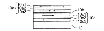
次に、本発明の第2実施形態による磁気メモリを、図6乃至図8を参照して説明する。図6は、本実施形態による磁気メモリのメモリセルの構成を示す断面図である。この実施形態による磁気メモリのメモリセル1Aは、図1に示す第1実施形態の磁気メモリの各メモリセルにおいて、磁気抵抗効果素子2を磁気抵抗効果素子2Aに置き換えた構成となっている。磁気抵抗効果素子2Aは、図1に示す磁気抵抗効果素子1の磁気記録層10のソフト層10aを、磁性層10a1、非磁性導電層10a2、磁性層10a3からなる3層構造とし、ハード層10cを、磁性層10c1、非磁性導電層10c2、磁性層10c3からなる3層構造とした構成となっている。ソフト層10aの磁性層10a1と磁性層10a3は強磁性結合をし、ハード層10cの磁性層10c1と磁性層10c3は反強磁性結合をしている。なお、ビット線20は本体部(破線部分)がワード線30と略並行に配置され、上記本体部から分岐した分岐部に磁気抵抗効果素子2の反強磁性層4が接続されるように構成されている。
(Second Embodiment)
Next, a magnetic memory according to a second embodiment of the present invention will be described with reference to FIGS. FIG. 6 is a cross-sectional view showing the configuration of the memory cell of the magnetic memory according to the present embodiment. The
なお、この第2実施形態におけるデータの書き込みおよび読み出し動作は、第1実施形態の場合と同じである。 The data write and read operations in the second embodiment are the same as those in the first embodiment.
この実施形態の磁気メモリも第1実施形態と同様に、書き込み電流はトンネルバリア層8を流れないため、トンネルバリア層が破壊されることがなく、信頼性の高いものとなる。また、磁気記録層10の体積は第1実施形態に比べて大きくすることが可能となり、微細化しても熱安定性が確保することができるとともに、微細セルの場合にスピン注入するとき、より低電流で磁気記録層10のスピン反転が可能となる。
Similarly to the first embodiment, since the write current does not flow through the
なお、第2実施形態においては、磁気抵抗効果素子2Aは引き出し電極18上に形成されていたが、引き出し電極18の下側に形成してもよい。この場合、磁気抵抗効果素子2Aの積層膜の積層順序が本実施形態と全く逆になり、ビット線20、ワード線30も引き出し電極18の下側に位置することになる。そして、この場合、ワード線30と接続部50が交差しないようにワード線30の位置をずらす必要がある。
In the second embodiment, the
(第1変形例)
次に、第2実施形態による磁気メモリの第1変形例を、図7を参照して説明する。この第1変形例の磁気メモリは、図6に示す第2実施形態の磁気メモリの各メモリセルにおいて、磁気抵抗効果素子2Aを図7に示す磁気抵抗効果素子に置き換えた構成となっている。図7に示す磁気抵抗効果素子は、ハード層10c、非磁性層10b、およびソフト層10aからなる共通の磁気記録層10上に2つの磁気抵抗効果素子2a、2bを設けた構成となっている。すなわち、磁気抵抗効果素子2aは、ソフト層10aの上面の一部分の領域上に形成された、トンネルバリア層8a、磁化固着層6a、反強磁性層4aからなる積層膜を有し、磁気抵抗効果素子2bは、ソフト層10aの上面の他の部分の領域上に形成された、トンネルバリア層8b、磁化固着層6b、反強磁性層4bからなる積層膜を有している。そして、磁気抵抗効果素子2aの反強磁性層4aはビット線20に接続され、磁気抵抗効果素子2bの反強磁性層4bは、キャップ層20aおよびビア27を介してワード線30に接続される構成となっている。なお、ソフト層10aは、第2実施形態と同様に、磁性層10a1、非磁性導電層10a2、磁性層10a3からなる積層構造であり、ハード層10cは、磁性層10c1、非磁性導電層10c2,磁性層10c3からなる積層構造である。
(First modification)
Next, a first modification of the magnetic memory according to the second embodiment will be described with reference to FIG. The magnetic memory of this first modification has a configuration in which the
この第1変形例においては、データの読み出しには、磁気抵抗効果素子2aに電流を流し、データの書き込みには磁気抵抗効果素子2bに電流を流す。これにより、第1変形例の構造を用いれば、読み出し時には通電する電流が小さいため、トンネルバリア層8aの絶縁破壊は起きないばかりか、書き込み時には磁気抵抗効果素子2aに電流が流れないため読み出しラインの磁気抵抗効果素子2aが破壊されることは無い。磁気抵抗効果素子2bのトンネルバリアはその際破壊される可能性があるが、破壊されても、スピン注入書き込みに問題は生じない。つまり、本変形例の構造を用いれば、作成上の容易性ばかりか、素子破壊が無い信頼性ある磁気メモリを実現することができる。
In this first modification, a current is passed through the
なお、この第1変形例においても、第2実施形態で説明したように、磁気抵抗効果素子2a,2bを引き出し電極18の下側に形成してもよい。
In the first modification, as described in the second embodiment, the
(第2変形例)
次に、第2実施形態による磁気メモリの第2変形例を、図8を参照して説明する。この第2変形例の磁気メモリは、図6に示す第2実施形態の磁気メモリの各メモリセルにおいて、磁気抵抗効果素子2Aを図8に示す磁気抵抗効果素子に置き換えた構成となっている。図8に示す磁気抵抗効果素子は、図6に示す磁気抵抗効果素子2の磁気記録層10のハード層10cと下地層16との間に反強磁性層12を設けた構成となっている。この反強磁性層12との交換結合力によってハード層10cの磁化(スピン)の向きが固着される。
(Second modification)
Next, a second modification of the magnetic memory according to the second embodiment will be described with reference to FIG. The magnetic memory of the second modification has a configuration in which the
この第2変形例も第2実施形態と同様に、書き込み電流によってトンネルバリア層8に破壊が生じず、信頼性の高いものとなる。
Similarly to the second embodiment, the second modification is also reliable because the
また、この第2変形例の構造を用いることにより、ハード層10cのスピンの向きが固着されているため、第2実施形態に比べてより低電流でスピンの向きを反転させることができる。
In addition, by using the structure of the second modification, the spin direction of the
なお、上記第2実施形態、第1変形例、および第2変形例においては、磁化固着層6は磁性層からなる単層であったが、シンセティックな構造、すなわち非磁性層を挟んで反強磁性結合の磁性層が積層された構造であってもよい。
In the second embodiment, the first modified example, and the second modified example, the magnetization pinned
また、上記第2実施形態、第1変形例、および第2変形例においては、磁気記録層10のソフト層10aおよびハード層10cは、非磁性導電層を挟んで磁性層が積層された3層構造であったが、非磁性導電層を介して磁性層が積層された5層以上の多層構造であってもよい。
In the second embodiment, the first modification, and the second modification, the
(第3実施形態)
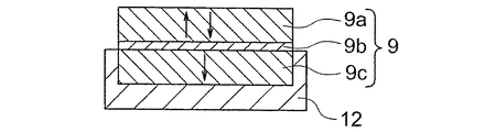
次に、本発明の第3実施形態による磁気メモリを、図9乃至図11を参照して説明する。図9は、本実施形態による磁気メモリのメモリセルの構成を示す断面図である。この実施形態による磁気メモリのメモリセル1Bは、図1に示す第1実施形態の磁気メモリの各メモリセルにおいて、磁気抵抗効果素子2を磁気抵抗効果素子2Bに置き換えた構成となっている。磁気抵抗効果素子2Bは、図1に示す磁気抵抗効果素子2において、磁化固着層6をスピンモーメントが膜厚方向(膜面に垂直方向)に向いた磁化固着層5に置き換えるとともに、磁気記録層10をスピンモーメントが膜厚方向に向いた磁気記録層9に置き換えた構成となっている。磁気記録層9は、磁化の向きが可変の磁性層からなるソフト層9aと、非磁性導電層9bと、磁化の向きが磁化固着層6の磁化の向きと反対の磁性層からなるハード層9cを有している。
(Third embodiment)
Next, a magnetic memory according to a third embodiment of the present invention will be described with reference to FIGS. FIG. 9 is a cross-sectional view showing the configuration of the memory cell of the magnetic memory according to the present embodiment. The
ハード層9cは、下地層16を介して引き出し電極18上に形成されている。ソフト層9aの上面の一部分の領域上にトンネルバリア層8が形成されている。トンネルバリア層8上には磁化固着層5が形成され、磁化固着層5上に反強磁性層4が形成されている。なお、磁化固着層5は上面および側面が反強磁性層4によって覆われている。ソフト層9aの上面の他の部分が接続部32を介してワード線30に接続されている。なお、ビット線20は本体部(破線部分)がワード線30と略並行に配置され、上記本体部から分岐した分岐部に磁気抵抗効果素子2の反強磁性層4が接続されるように構成されている。
The
なお、この第3実施形態におけるデータの書き込みおよび読み出し動作は、第1実施形態の場合と同じである。 The data write and read operations in the third embodiment are the same as those in the first embodiment.
この第3実施形態による磁気メモリにおいても、第1実施形態と同様に、書き込み時には電流がトンネルバリア層8を流れないため、トンネルバリア層8が破壊されることがなく、信頼性の高いものとなる。また、磁気記録層9の体積を大きくすることが可能となり、微細化しても熱安定性が確保することができるとともに、微細セルの場合にスピン注入するとき、より低電流で磁気記録層9のスピン反転ができ、消費電力を少なくすることができる。
In the magnetic memory according to the third embodiment, as in the first embodiment, since no current flows through the
なお、第3実施形態においては、磁気抵抗効果素子2Bは引き出し電極18上に形成されていたが、引き出し電極18の下側に形成してもよい。この場合、磁気抵抗効果素子2Bの積層膜の積層順序が本実施形態と全く逆になり、ビット線20、ワード線30も引き出し電極18の下側に位置することになる。そして、この場合、ワード線30と接続部50が交差しないようにワード線30の位置をずらす必要がある。
In the third embodiment, the
(第1変形例)
次に、第3実施形態による磁気メモリの第1変形例を、図10を参照して説明する。この第1変形例の磁気メモリは、図9に示す第1実施形態の磁気メモリの各メモリセルにおいて、磁気抵抗効果素子2Bを図10に示す磁気抵抗効果素子に置き換えた構成となっている。図10に示す磁気抵抗効果素子は、ハード層9c、非磁性層9b、およびソフト層9aからなる共通の磁気記録層9上に2つの磁気抵抗効果素子2a、2bを設けた構成となっている。すなわち、磁気抵抗効果素子2aは、ソフト層9aの上面の一部分の領域上に形成された、トンネルバリア層8a、磁化固着層5a、反強磁性層4aからなる積層膜を有し、磁気抵抗効果素子2bは、ソフト層9aの上面の他の部分の領域上に形成された、トンネルバリア層8b、磁化固着層5b、反強磁性層4bからなる積層膜を有している。そして、磁気抵抗効果素子2aの反強磁性層4aはビット線20に接続され、磁気抵抗効果素子2bの反強磁性層4bは、キャップ層20aおよびビア27を介してワード線30に接続される構成となっている。
(First modification)
Next, a first modification of the magnetic memory according to the third embodiment will be described with reference to FIG. The magnetic memory of the first modified example has a configuration in which the
この第1変形例においては、データの読み出しには、磁気抵抗効果素子2aに電流を流し、データの書き込みには磁気抵抗効果素子2bに電流を流す。これにより、第1変形例の構造を用いれば、読み出し時には通電する電流が小さいため、トンネルバリア層8aの絶縁破壊は起きないばかりか、書き込み時には磁気抵抗効果素子2aに電流が流れないため読み出しラインの磁気抵抗効果素子2aが破壊されることは無い。磁気抵抗効果素子2bのトンネルバリアはその際破壊される可能性があるが、破壊されても、スピン注入書き込みに問題は生じない。つまり、本変形例の構造を用いれば、作成上の容易性ばかりか、素子破壊が無い信頼性ある磁気メモリを実現することができる。
In this first modification, a current is passed through the
なお、この第1変形例においても、第3実施形態で説明したように、磁気抵抗効果素子2a,2bを引き出し電極18の下側に形成してもよい。
In the first modification, as described in the third embodiment, the
(第2変形例)
次に、第3実施形態による磁気メモリの第2変形例を、図11を参照して説明する。この第2変形例の磁気メモリは、図9に示す第1実施形態の磁気メモリの各メモリセルにおいて、磁気抵抗効果素子2Bを図11に示す磁気抵抗効果素子に置き換えた構成となっている。図11に示す磁気抵抗効果素子は、図9に示す磁気抵抗効果素子2の磁気記録層9のハード層9cと下地層16との間に反強磁性層12を設けた構成となっている。この反強磁性層12との交換結合力によってハード層9cの磁化(スピン)の向きが固着される。なお、反強磁性層12は、ハード層9cの下面および側面を覆っている。
(Second modification)
Next, a second modification of the magnetic memory according to the third embodiment will be described with reference to FIG. The magnetic memory of the second modification has a configuration in which the
この第2変形例も第1実施形態と同様に、書き込み電流によってトンネルバリア層8に破壊が生じず、信頼性の高いものとなる。
Similarly to the first embodiment, the second modification is also reliable because the
また、この第2変形例の構造を用いることにより、ハード層9cのスピンの向きが固着されているため、第3実施形態に比べてより低電流でスピンの向きを反転させることができる。
Further, by using the structure of the second modification, the spin direction of the
(第4実施形態)
次に、本発明の第4実施形態による磁気メモリを、図12を参照して説明する。図12は、本実施形態による磁気メモリのメモリセルの構成を示す断面図である。この実施形態による磁気メモリのメモリセル1Cは、図1に示す第1実施形態の磁気メモリの各メモリセルにおいて、磁気抵抗効果素子2を磁気抵抗効果素子2Cに置き換えた構成となっている。
(Fourth embodiment)
Next, a magnetic memory according to a fourth embodiment of the present invention is described with reference to FIG. FIG. 12 is a cross-sectional view showing the configuration of the memory cell of the magnetic memory according to the present embodiment. The
磁気抵抗効果素子2Cは、ワード線20上に形成された反強磁性層4と、反強磁性層4上に形成された磁化固着層6と、磁化固着層6上に形成されたトンネルバリア層8と、トンネルバリア層8上に形成された磁気記録層10とを備えている。すなわち、磁気抵抗効果素子1Cは、磁化固着層6が磁気記録層10に比べて下側に配置されたボトムピン型の磁気抵抗効果素子である。
The
磁気記録層10は、ソフト層10aと、ソフト層10a上に形成された非磁性導電層10bと、非磁性導電層10bの上面の一部分の領域上に形成されたハード層10cとを有している。ソフト層10aは、トンネルバリア層8上に形成された磁性層10a1と、この磁性層10a1上に形成された非磁性導電層10a2と、非磁性層10a2上に形成された磁性層10a3とからなっている。ハード層10cは、非磁性導電層10bの上面の一部分の領域上に形成された磁性層10c1と、この磁性層10c1上に形成された非磁性導電層10c2と、非磁性導電層10c2上に形成された磁性層10c3とからなっている。磁性層10c3は、キャップ層17を介して引き出し電極18の下面に接続されている。非磁性導電層10bの上面の他の部分は接続部32を介してワード線30に接続された構成となっている。なお、ビット線20は本体部(破線部分)がワード線30と略並行に配置され、上記本体部から分岐した分岐部に磁気抵抗効果素子2の反強磁性層4が接続されるように構成されている。また、本実施形態においては、ワード線30は接続部32を介して非磁性導電層10bに接続されていたが、接続部32と磁性層10a3間の非磁性導電層10bを除去して接続部32が磁性層10a3に接続されるように構成してもよい。
The
なお、この第4実施形態におけるデータの書き込みおよび読み出し動作は、第1実施形態の場合と同じである。例えば、書き込み電流はワード線30、接続部32、非磁性導電層10b、ソフト層10a、ハード層10c、キャップ層17、引き出し電極18、接続部50、選択トランジスタ60の順に流れる。
The data write and read operations in the fourth embodiment are the same as those in the first embodiment. For example, the write current flows in the order of the
この第4実施形態においても、第1実施形態と同様に、書き込み時には、スピン注入のための電流はトンネルバリア層8を流れないため、トンネルバリア層8が絶縁破壊されることがなく、信頼性の高いものとなる。また、書き込みがスピン注入によって行われるため、電流磁界による書き込みに比べて低い電流で行うことが可能となり、消費電力を少なくすることができる。
Also in the fourth embodiment, as in the first embodiment, the current for spin injection does not flow through the
なお、第4実施形態において、ハード層10cの磁性層10c3と、キャップ層17との間に反強磁性層を設け、この反強磁性層との交換結合力によってハード層10cの磁化の向きを固着するようにしてもよい。この場合、第4実施形態に比べて、より低電流でソフト層10aの磁化の向きを反転することが可能となる。
In the fourth embodiment, an antiferromagnetic layer is provided between the magnetic layer 10c3 of the
なお、第4実施形態においては、磁気抵抗効果素子2Cは引き出し電極18下に形成されていたが、引き出し電極18の上側に形成してもよい。この場合、磁気抵抗効果素子2Cの積層膜の積層順序が本実施形態と全く逆になり、ビット線20が引き出し電極18の上側に、ワード線30が、引き出し電極18の下側に位置することになる。そして、この場合、ワード線30と接続部50が交差しないようにワード線30の位置をずらす必要がある。
In the fourth embodiment, the
(第5実施形態)
次に、本発明の第5実施形態による磁気メモリを、図13を参照して説明する。図13は、本実施形態による磁気メモリのメモリセルの構成を示す断面図である。この実施形態による磁気メモリのメモリセル1Dは、図12に示す第4実施形態の磁気メモリ1Cにおいて、磁気抵抗効果素子2Cを磁気抵抗効果素子2Dに置き換えた構成となっている。
(Fifth embodiment)
Next, a magnetic memory according to a fifth embodiment of the present invention is described with reference to FIG. FIG. 13 is a cross-sectional view showing the configuration of the memory cell of the magnetic memory according to the present embodiment. The
磁気抵抗効果素子2Dは、ワード線20上に形成された反強磁性層4と、反強磁性層4上に形成され磁化の向きが膜面に垂直の磁化固着層5と、磁化固着層5上に形成されたトンネルバリア層8と、トンネルバリア層8上に形成された磁気記録層9とを備えている。すなわち、磁気抵抗効果素子1Cは、磁化固着層5が磁気記録層9に比べて下側に配置されたボトムピン型の磁気抵抗効果素子である。なお、反強磁性層4によって磁化固着層5の下面および側面が覆われている。
The
磁気記録層9は、磁化の向きが膜面に垂直な磁性層からなるソフト層9aと、ソフト層9a上に形成された非磁性導電層9bと、非磁性導電層9bの上面の一部分の領域上に形成された磁化の向きが膜面に垂直なハード層9cとを有している。ハード層9cは、キャップ層17を介して引き出し電極18の下面に接続されている。非磁性導電層10bの上面の他の部分は接続部32を介してワード線30に接続された構成となっている。なお、ビット線20は本体部(破線部分)がワード線30と略並行に配置され、上記本体部から分岐した分岐部に磁気抵抗効果素子2の反強磁性層4が接続されるように構成されている。また、本実施形態においては、ワード線30は接続部32を介して非磁性導電層9bに接続されていたが、接続部32とソフト層9a間の非磁性導電層9bを除去して接続部32がソフト層9aに接続されるように構成してもよい。
The
なお、この第3実施形態におけるデータの書き込みおよび読み出し動作は、第4実施形態の場合と同じである。 The data write and read operations in the third embodiment are the same as those in the fourth embodiment.
この第5実施形態においても、第4実施形態と同様に、書き込み時には、スピン注入のための電流はトンネルバリア層8を流れないため、トンネルバリア層8が絶縁破壊されることがなく、信頼性の高いものとなる。また、書き込みがスピン注入によって行われるため、電流磁界による書き込みに比べて低い電流で行うことが可能となり、消費電力を少なくすることができる。
Also in the fifth embodiment, as in the fourth embodiment, the current for spin injection does not flow through the
なお、第5実施形態において、ハード層9cと、キャップ層17との間に反強磁性層を設け、この反強磁性層との交換結合力によってハード層9cの磁化の向きを固着するようにしてもよい。この場合、第5実施形態に比べて、より低電流でソフト層9aの磁化の向きを反転することが可能となる。
In the fifth embodiment, an antiferromagnetic layer is provided between the
なお、第5実施形態においては、磁気抵抗効果素子2Dは引き出し電極18下に形成されていたが、引き出し電極18の上側に形成してもよい。この場合、磁気抵抗効果素子2Dの積層膜の積層順序が本実施形態と全く逆になり、ビット線20が引き出し電極18の上側に、ワード線30が引き出し電極18の下側に位置することになる。そして、この場合、ワード線30と接続部50が交差しないようにワード線30の位置をずらす必要がある。
In the fifth embodiment, the
(第6実施形態)
次に、本発明の第6実施形態による磁気メモリを、図14を参照して説明する。図14は、本実施形態による磁気メモリのメモリセルの構成を示す断面図である。本実施形態による磁気メモリは、アレイ状に配置された複数のメモリセル1Eを有しており、各メモリセル1Eは、図14に示すように、磁気抵抗効果素子2Ea、2Ebと、引き出し部28と、ビット線20a、20bと、ワード線30と、接続部50と、選択トランジスタ60とを備えている。接続部50は、接続プラグ52、54、56を有しており、選択トランジスタ60は、ゲート62と、ドレイン64と、ソース66とを有している。なお、図14においては、ワード線30の断面と選択トランジスタ60の断面があたかも同一断面となるように記載されているが、実際には選択トランジスタ60の断面は、ワード線30の断面と略直交する位置における断面である。すなわち、ワード線30と選択トランジスタ60のゲート62は、略直交するように配置されている。
(Sixth embodiment)
Next, a magnetic memory according to a sixth embodiment of the present invention is described with reference to FIG. FIG. 14 is a cross-sectional view showing the configuration of the memory cell of the magnetic memory according to the present embodiment. The magnetic memory according to the present embodiment has a plurality of
磁気抵抗効果素子2Eaと、磁気抵抗効果素子2Ebとは、磁気記録層10およびこの磁気記録層10上に形成されたトンネルバリア層8が共通に形成された構成となっている。磁気記録層10は、ソフト層10aと、非磁性層10bと、ハード層10cとを備えている。ハード層10cは、ワード線30上に形成された磁性層10c3と、磁性層10c3上に形成された非磁性導電層10c2と、非磁性導電層10c2上に形成された磁性層10c1とから構成されている。非磁性層10bは磁性層10c1上に形成されている。ソフト層10aは、非磁性層10b上に形成された磁性層10a3と、磁性層10a3上に形成された非磁性導電層10a2と、非磁性導電層10a2上に形成された磁性層10a1とからなっている。トンネルバリア層8は磁性層10a1上に形成されている。
The magnetoresistive effect element 2Ea and the magnetoresistive effect element 2Eb have a configuration in which the
磁気抵抗効果素子2Eaは、更にトンネルバリア層8の上面の第1領域に形成された磁化固着層6aと、磁化固着層6a上に形成された反強磁性層4aとを有し、磁気抵抗効果素子2Ebは、トンネルバリア層8の上面の第2領域に形成された磁化固着層6bと、磁化固着層6b上に形成された反強磁性層4bとを有している。反強磁性層4aはビット線20aに接続され、反強磁性層4bはビット線20bに接続されている。なお、磁化固着層6aと磁化固着層6bのうちの少なくとも一方は、シンセティックな磁化固着層すなわち非磁性層を挟んで反強磁性結合の磁性層が積層された構造であってもよい。この場合、シンセティックな磁化固着層上の反強磁性層は不要としてもよい。
The magnetoresistive effect element 2Ea further includes a magnetic pinned
また、トンネルバリア層8の第3領域が引き出し部28および接続部50を介して選択トランジスタ60のドレインに接続されている。
Further, the third region of the
本実施形態においては、書き込み動作は、第1実施形態の場合と同様に、選択トランジスタ60をONして、ワード線30と選択トランジスタ60のソース66との間に電流を流し、磁気記録層10にスピン注入することにより行う。また、読み出し動作は、選択トランジスタ60をONし、選択トランジスタ60のソース66からドレイン64、接続部50、引き出し部28を介して電流を流す。すると、この電流はソフト層10aで磁気抵抗効果素子2Eaおよび磁気抵抗効果素子2Ebに分岐され、それぞれビット線20aおよびビット線20bに流れる。このとき、ビット線20a、20bに流れる電流を差動増幅器86で読み出すことにより、メモリセルからのデータの読み出しを行う。この場合、高速の読み出しが可能となる。
In the present embodiment, as in the case of the first embodiment, in the write operation, the
この実施形態も、書き込み動作時には、トンネルバリア層8の第3領域と、ワード線30との間にスピン注入のための電流が流れ、磁化固着層6a、6b直下のトンネルバリア層8にはほとんどスピン注入のための電流が流れないため、磁化固着層6a、6b直下のトンネルバリア層8が絶縁破壊されることがなく、信頼性の高いものとなる。また、書き込みがスピン注入によって行われるため、電流磁界による書き込みに比べて低い電流で行うことが可能となり、消費電力を少なくすることができる。
Also in this embodiment, during the write operation, a current for spin injection flows between the third region of the
なお、第6実施形態において、図15に示すように、引き出し部28と、トンネルバリア層8の第3領域との間に、磁化固着層6c、反強磁性層4c、およびキャップ層20cからなる積層膜を挿入してもよい。この場合には、磁気抵抗効果素子2Ea、2Ebを覆う層間絶縁膜を平坦化し易いという製造工程メリットがある。
In the sixth embodiment, as shown in FIG. 15, the pinned
なお、第6実施形態においては、磁気抵抗効果素子2Ea、2Ebはワード線30上に形成されていたが、ワード線30の下側に形成してもよい。この場合、磁気抵抗効果素子2Ea、2Ebの積層膜の積層順序が本実施形態と全く逆になり、ビット線20a、20bおよび引き出し部28がワード線30の下側に位置することになる。
In the sixth embodiment, the magnetoresistive elements 2Ea and 2Eb are formed on the
なお、本実施形態においては、引き出し部28はトンネルバリア層8に接続するように構成されていたが、引き出し部28とソフト層10aの磁性層10a1との間のトンネルバリア層8を除去して引き出し部28が磁性層10a1に直接接続されるように構成してもよい。この場合は、磁化固着層6aと磁性層10a1との間のトンネルバリア層8と、磁化固着層6bと磁性層10a1との間のトンネルバリア層8とは同じ材料で形成してもよいし、異なる材料で形成してもよい。
In the present embodiment, the
(第7実施形態)
次に、本発明の第7実施形態による磁気メモリを図16を参照して説明する。図16は、本実施形態による磁気メモリのメモリセルの構成を示す断面図である。本実施形態による磁気メモリは、アレイ状に配置された複数のメモリセル1Fを有しており、各メモリセル1Fは、図16に示すように、磁気抵抗効果素子2Fa、2Fbと、引き出し部28と、ビット線20a、20bと、ワード線30と、接続部50と、選択トランジスタ60とを備えている。接続部50は、接続プラグ52、54、56を有しており、選択トランジスタ60は、ゲート62と、ドレイン64と、ソース66とを有している。
(Seventh embodiment)
Next, a magnetic memory according to a seventh embodiment of the present invention is described with reference to FIG. FIG. 16 is a cross-sectional view showing the configuration of the memory cell of the magnetic memory according to the present embodiment. The magnetic memory according to the present embodiment has a plurality of
磁気抵抗効果素子2Faと、磁気抵抗効果素子2Fbとは、磁化の向きが膜面に垂直な磁気記録層9およびこの磁気記録層9上に形成されたトンネルバリア層8が共通に形成された構成となっている。磁気記録層9は、ソフト層9aと、非磁性層9bと、ハード層9cとを備えている。なお、図16においては、ワード線30の断面と選択トランジスタ60の断面があたかも同一断面となるように記載されているが、実際には選択トランジスタ60の断面は、ワード線30の断面と略直交する位置における断面である。すなわち、ワード線30と選択トランジスタ60のゲート62は、略直交するように配置されている。
The magnetoresistive effect element 2Fa and the magnetoresistive effect element 2Fb have a configuration in which the
磁気抵抗効果素子2Faは、更にトンネルバリア層8の上面の第1領域に形成された磁化の向きが膜面に垂直な磁化固着層5aと、磁化固着層5aの上面および側面に形成された反強磁性層4aとを有し、磁気抵抗効果素子2Fbは、トンネルバリア層8の上面の第2領域に形成された磁化の向きが膜面に垂直な磁化固着層5bと、磁化固着層5bの上面および側面に形成された反強磁性層4bとを有している。反強磁性層4aはビット線20aに接続され、反強磁性層4bはビット線20bに接続されている。
The magnetoresistive effect element 2Fa further includes a magnetization pinned
また、トンネルバリア層8の第3領域が引き出し部28および接続部50を介して選択トランジスタ60のドレインに接続されている。
Further, the third region of the
本実施形態においては、書き込み動作は、第1実施形態の場合と同様に、選択トランジスタ60をONして、ワード線30と選択トランジスタ60のソース66との間に電流を流し、磁気記録層10にスピン注入することにより行う。また、読み出し動作は、選択トランジスタ60をONし、選択トランジスタ60のソース66からドレイン64、接続部50、引き出し部28を介して電流を流す。すると、この電流はソフト層9aで磁気抵抗効果素子2Faおよび磁気抵抗効果素子2Fbに分岐され、それぞれビット線20aおよびビット線20bに流れる。このとき、ビット線20a、20bに流れる電流を差動増幅器86で読み出すことにより、メモリセルからのデータの読み出しを行う。この場合、高速の読み出しが可能となる。
In the present embodiment, as in the case of the first embodiment, in the write operation, the
この実施形態も、書き込み動作時には、トンネルバリア層8の第3領域と、ワード線30との間にスピン注入のための電流が流れ、磁化固着層5a、5b直下のトンネルバリア層8にはほとんどスピン注入のための電流が流れないため、磁化固着層5a、5b直下のトンネルバリア層8が絶縁破壊されることがなく、信頼性の高いものとなる。また、書き込みがスピン注入によって行われるため、電流磁界による書き込みに比べて低い電流で行うことが可能となり、消費電力を少なくすることができる。
Also in this embodiment, a current for spin injection flows between the third region of the
なお、第7実施形態においては、磁気抵抗効果素子2Fa、2Fbはワード線30上に形成されていたが、ワード線30の下側に形成してもよい。この場合、磁気抵抗効果素子2Fa、2Fbの積層膜の積層順序が本実施形態と全く逆になり、ビット線20a、20bおよび引き出し部28がワード線30の下側に位置することになる。
In the seventh embodiment, the magnetoresistive elements 2Fa and 2Fb are formed on the
なお、第7実施形態において、図17に示すように、引き出し部28と、トンネルバリア層8の第3領域との間に、磁化の向きが膜面に垂直な磁化固着層5c、反強磁性層4c、およびキャップ層20cからなる積層膜を挿入してもよい。この場合には、磁気抵抗効果素子2Fa、2Fbを覆う層間絶縁膜を平坦化し易いという製造工程メリットがある。
In the seventh embodiment, as shown in FIG. 17, a magnetization pinned layer 5 c whose magnetization direction is perpendicular to the film surface, antiferromagnetic, between the lead-out
なお、第7実施形態においては、引き出し部28はトンネルバリア層8に接続するように構成されていたが、引き出し部28とソフト層9aとの間のトンネルバリア層8を除去して引き出し部28がソフト層9aに直接接続されるように構成してもよい。この場合は、磁化固着層5aとソフト層9aとの間のトンネルバリア層8と、磁化固着層5bとソフト層9aとの間のトンネルバリア層8とは、同じ材料で形成してもよいし、異なる材料で形成してもよい。
In the seventh embodiment, the
上記第1乃至第7実施形態においては、磁気メモリのメモリセルの構成について説明したが、上記実施形態の磁気メモリの回路構成の一具体例を図18に示す。なお、図18は、第1実施形態による磁気メモリの回路構成を示しているが、第2乃至第7実施形態による磁気メモリについても同じ回路構成とすることが可能である。また、後述する第8実施形態の磁気メモリも同じ回路構成とすることができる。 In the first to seventh embodiments, the configuration of the memory cell of the magnetic memory has been described. FIG. 18 shows a specific example of the circuit configuration of the magnetic memory of the above embodiment. FIG. 18 shows the circuit configuration of the magnetic memory according to the first embodiment, but the same circuit configuration can be applied to the magnetic memory according to the second to seventh embodiments. Also, the magnetic memory of the eighth embodiment to be described later can have the same circuit configuration.
図18において、磁気メモリは、複数のビット線20と、これらのビット線20に並行するように形成された複数のワード線30と、アレイ状に配置された複数のメモリセル1と、ビット線20を選択するビット線選択トランジスタ90と、ワード線30を選択するワード線選択トランジスタ92とを備えている。各メモリセル1は、磁気抵抗効果素子2と、選択トランジスタ60とを備えている。磁気抵抗効果素子2の磁化固着層6はビット線20に接続される。磁気抵抗効果素子2のトンネルバリア層8と磁気記録層10との接続点がワード線30に接続される。なお、同一行のメモリセルの選択トランジスタ60はゲートが接続された構成となっている。
18, the magnetic memory includes a plurality of
メモリセル1へのデータの書き込みは、選択すべきワード線30に接続されたワード線選択トランジスタ92をONするとともに書き込むべきメモリセルの選択トランジスタ60をONして、選択したワード線30に電流を流し、磁気記録層10にスピン注入することによって行う。一方読み出しは、選択すべきビット線に接続されたビット線選択トランジスタ90をONするとともに読み出すべきメモリセルの選択トランジスタ60をONし、ビット線20からメモリセル1に電流が流れるように電圧を印加し、流れた電流を検出することにより行う。
Data is written to the
なお、図18に示す回路において、磁気抵抗効果素子に流すセンス電流を制御するセンス電流制御回路(図示せず)、ドライバ(図示せず)、およびシンカー(図示せず)を更に備えている。 Note that the circuit shown in FIG. 18 further includes a sense current control circuit (not shown) for controlling the sense current to flow through the magnetoresistive element, a driver (not shown), and a sinker (not shown).
(第8実施形態)
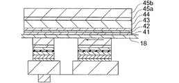
次に、本発明の第8実施形態による磁気メモリを、図19を参照して説明する。図19は、本実施形態による磁気メモリのメモリセルの構成を示す断面図である。本実施形態による磁気メモリは、アレイ状に配置された複数のメモリセル1Gを有しており、各メモリセル1Gは、図19に示すように、磁気抵抗効果素子21、22と、引き出し電極18と、ビット線20と、ワード線30と、磁気抵抗効果素子40と、接続部50と、選択トランジスタ60とを備えている。接続部50は、接続プラグ52、54、56を有しており、選択トランジスタ60は、ゲート62と、ドレイン64と、ソース66とを有している。接続プラグ56はドレイン64と電気的に接続される。
(Eighth embodiment)
Next, a magnetic memory according to an eighth embodiment of the present invention is described with reference to FIG. FIG. 19 is a cross-sectional view showing the configuration of the memory cell of the magnetic memory according to the present embodiment. The magnetic memory according to the present embodiment has a plurality of
磁気抵抗効果素子21と、磁気抵抗効果素子22は、同じ層構造を有している。すなわち、磁気抵抗効果素子2i(i=1,2)は、下地層25iと、下地層25i上に形成された反強磁性層4iと、反強磁性層4i上に形成された磁化固着層6iと、磁化固着層6i上にトンネルバリア層81を介して形成された磁気記録層10iとを備えている。そして、磁気抵抗効果素子21の下地層251はビット線20上に形成され、磁気記録層101は引き出し電極18に接続される。また、磁気抵抗効果素子22の下地層252は接続部50の接続プラグ52上に形成され、磁気記録層102は引き出し電極18に接続される。すなわち、磁気抵抗効果素子21はビット線20と引き出し電極18との間に形成され、磁気抵抗効果素子22は接続プラグ52と引き出し電極18との間に形成された構成となっている。なお、ビット線20は本体部(破線部分)がワード線30と略並行に配置され、上記本体部から分岐した分岐部に磁気抵抗効果素子21の反強磁性層41が接続されるように構成されている。
A
また、磁気抵抗効果素子40は、引き出し電極18上に形成された磁性層41と、磁性層41上に形成された金属または半導体からなる層42と、層42上に形成された磁化固着層43と、磁化固着層43上に形成された反強磁性層44と、反強磁性層44上に形成されたキャップ層45とを備えている。キャップ層45はワード線30に接続されている。また、磁気抵抗効果素子21の磁気記録層101と、磁性層41は、反強磁性結合または静磁結合の相互作用が働いており、スピンモーメントの向きは互いに逆方向を向いている。なお、磁化固着層61、62、43は、単層の磁性層であったが、シンセティック構造であってもよい。
In addition, the
本実施形態においては、書き込み動作は、図20に示すように、選択トランジスタ60をONして、ワード線30と選択トランジスタ60のソース66との間、すなわち磁気抵抗効果素子22と磁気抵抗効果素子40に電流を流し、磁性層41にスピン注入することにより行う。すると、磁性層41と反強磁性結合または静磁結合している磁気抵抗効果素子21の磁気記録層101のスピンの向きが、磁性層41のスピンの反転に応じて変わり、磁気記録層101にデータの書き込みが行われる。
In the present embodiment, the writing operation, as shown in FIG. 20, by turning ON the
また、読み出し動作は、図21に示すように、選択トランジスタ60をONし、ビット線20から磁気抵抗効果素子21、引き出し電極18、磁気抵抗効果素子22、接続部50、選択トランジスタ60のドレイン64、ソース66へ電流を流すことにより行われる。
In the read operation, as shown in FIG. 21, the
この実施形態も、書き込み動作時には、磁気抵抗効果素子21のトンネルバリア層81にはスピン注入のための電流が流れないため、トンネルバリア層81が絶縁破壊されることがなく、信頼性の高いものとなる。なお、書き込み時には、磁気抵抗効果素子22には電流が流れるが、この磁気抵抗効果素子22のトンネルバリア層82の破壊が起きてもスピン注入書き込みには悪影響を与えない。また、書き込みがスピン注入によって行われるため、電流磁界による書き込みに比べて低い電流で行うことが可能となり、消費電力を少なくすることができる。
This embodiment also, during a write operation, since the
なお、本実施形態においては、書き込み時に電流を流す磁性層41の膜厚が磁気記録層101に比べて厚いか、または実際のスピンモーメントが大きく漏れ磁界が大きい方が好ましい。実際には、磁性層41の厚さを厚くする、または磁気モーメントが大きな材料にすることで実現できる。
In the present embodiment, or the thickness of the
なお、第8実施形態においては、磁気抵抗効果素子21は引き出し電極18の下側に、磁気抵抗効果素子40は引き出し電極18の上側に形成されていたが、磁気抵抗効果素子21を引き出し電極18の上側に、磁気抵抗効果素子40を引き出し電極18の下側に形成してもよい。この場合、磁気抵抗効果素子21、40の積層膜の積層順序が本実施形態と全く逆になり、ビット線20が引き出し電極18の上側に、ワード線30が引き出し電極18の下側に位置することになる。また、この場合、ワード線30と接続部50が交差しないようにワード線30の位置をずらす必要がある。また、この場合、磁気抵抗効果素子22は、磁気抵抗効果素子40の積層膜の積層順序が逆にした構成となる。
In the eighth embodiment, the
(変形例)
次に、本発明の第8実施形態の変形例による磁気メモリの構成を図22に示す。この変形例による磁気メモリは、第8実施形態の磁気メモリにおいて、磁気記録層101と、磁性層41との反強磁性結合の強さを調整するために、引き出し電極18の一部に磁性層からなる、または磁性層/非磁性層からなる膜19を挿入したものである。磁気記録層101と磁性層41の相互作用は、その絶対値が0.2erg/cm2以下、より好ましくは0.1erg/cm2以下であることが好ましい。この大きさ以下では、熱擾乱耐性、磁気抵抗曲線の角型比など好ましい特性を得ることができる。
(Modification)
Next, FIG. 22 shows a configuration of a magnetic memory according to a modification of the eighth embodiment of the present invention. The magnetic memory according to this modification, in the magnetic memory of the eighth embodiment, a
(第9実施形態)
次に、本発明の第9実施形態による磁気メモリの構成を図23に示す。図23は、本実施形態による磁気メモリのメモリセルの構成を示す断面図である。この実施形態による磁気メモリは、図19に示す第8実施形態による磁気メモリにおいて、ビット線20の下方に、スピン注入時に微弱な電流磁界を、磁気記録層101のスピンモーメントの磁化容易軸方向に印加するためのデジット線70を設けた構成となっている。これは、スピントルクは、スピンモーメントが多少でも傾いていると有効にスピン反転するためである。なお、電流磁界をより小さな電流で発生させるために、デジット線70の下面および側面が磁性膜70aによって被覆されている。したがって、第8実施形態の場合よりも、より小さな電流で書き込みを行うことが可能となり、消費電力を少なくすることができる。なお、ビット線20の下方にデジット線70を設けたことにより、接続部50Aは、接続プラグ52と接続プラグ54との間に、接続プラグ53が設けられた構成となる。この接続プラグ53の下面および側面はデジット線70と同様に磁性膜53aによって被覆されている。
(Ninth embodiment)
Next, FIG. 23 shows a configuration of a magnetic memory according to the ninth embodiment of the present invention. FIG. 23 is a cross-sectional view showing the configuration of the memory cell of the magnetic memory according to the present embodiment. The magnetic memory according to this embodiment, in the magnetic memory according to the eighth embodiment shown in FIG. 19, below the bit lines 20, a weak current magnetic field at the time of spin injection magnetization easy axis direction of the spin moment of the
この実施形態による磁気メモリも、第8実施形態と同様に、書き込み動作時には、磁気抵抗効果素子21のトンネルバリア層81にはスピン注入のための電流が流れないため、トンネルバリア層81が絶縁破壊されることがなく、信頼性の高いものとなる。
Also magnetic memory according to this embodiment, like the eighth embodiment, during a write operation, since the
なお、第9実施形態においては、磁気抵抗効果素子21は引き出し電極18の下側に、磁気抵抗効果素子40は引き出し電極18の上側に形成されていたが、第8実施形態で説明したように、磁気抵抗効果素子21を引き出し電極18の上側に、磁気抵抗効果素子40を引き出し電極18の下側に形成してもよい。この場合、磁気抵抗効果素子21、40の積層膜の積層順序が本実施形態と全く逆になり、ビット線20が引き出し電極18の上側に、ワード線30が引き出し電極18の下側に位置することになるとともに、デジット線70はビット線20の上側に位置することになる。また、この場合、ワード線30と接続部50が交差しないようにワード線30の位置をずらす必要がある。また、この場合、磁気抵抗効果素子22は、磁気抵抗効果素子40の積層膜の積層順序が逆にした構成となる。
Incidentally, as in the ninth embodiment, the
(第10実施形態)
次に、本発明の第10実施形態による磁気メモリの構成を図24、図25に示す。図24は、本実施形態による磁気メモリのメモリセルの構成を示す断面図であり、図25は、図24に示す切断線A−Aによって切断した断面図である。この実施形態による磁気メモリは、図6に示す第2実施形態による磁気メモリにおいて、引き出し電極18の下方に、スピン注入時に微弱な電流磁界を、磁気記録層10のスピンモーメントの磁化容易軸方向に印加するためのデジット線70を設けた構成となっている。なお、電流磁界をより小さな電流で発生させるために、デジット線70の下面および側面が磁性膜70aによって被覆されている。したがって、第2実施形態の場合よりも、より小さな電流で書き込みを行うことが可能となり、消費電力を少なくすることができる。なお、接続部50の接続プラグ52は、下面および側面がデジット線70と同様に磁性膜52aによって被覆されている。
(10th Embodiment)
Next, the configuration of a magnetic memory according to the tenth embodiment of the present invention is shown in FIGS. 24 is a cross-sectional view showing the configuration of the memory cell of the magnetic memory according to the present embodiment, and FIG. 25 is a cross-sectional view taken along the cutting line AA shown in FIG. The magnetic memory according to this embodiment is the same as the magnetic memory according to the second embodiment shown in FIG. 6, but a weak current magnetic field is applied below the
この実施形態による磁気メモリも、第2実施形態と同様に、書き込み動作時には、磁気抵抗効果素子2Aのトンネルバリア層8にはスピン注入のための電流が流れないため、トンネルバリア層8が絶縁破壊されることがなく、信頼性の高いものとなる。
In the magnetic memory according to this embodiment, as in the second embodiment, the current for the spin injection does not flow through the
なお、第10実施形態において、磁気記録層10のハード層10cと、引き出し電極18との間に図26に示すように、反強磁性層12を設けても良い。この反強磁性層12との交換結合力によってハード層10cの磁化(スピン)の向きが固着されるため、さらにより低電流でスピンの向きを反転させることができる。
In the tenth embodiment, an
なお、第10実施形態においては、磁気抵抗効果素子2Aは引き出し電極18上に形成されていたが、第2実施形態で説明したように、引き出し電極18の下側に形成してもよい。この場合、磁気抵抗効果素子2Aの積層膜の積層順序が本実施形態と全く逆になり、ビット線20、ワード線30も引き出し電極18の下側に位置するとともにデジット線70が引き出し電極18の上側に位置することになる。そして、この場合、ワード線30と接続部50が交差しないようにワード線30の位置をずらす必要がある。
In the tenth embodiment, the
(第11実施形態)
次に、本発明の第11実施形態による磁気メモリの構成を図27を参照して説明する。図27は、本実施形態による磁気メモリのメモリセルの構成を示す断面図である。本実施形態による磁気メモリは、図12に示す第4実施形態による磁気メモリにおいて、ビット線20の下方、スピン注入時に微弱な電流磁界を、磁気記録層10のスピンモーメントの磁化容易軸方向に印加するためのデジット線70を設けた構成となっている。なお、電流磁界をより小さな電流で発生させるために、デジット線70の下面および側面が磁性膜70aによって被覆されている。このようにデジット線70を設けるとともにデジット線70を磁性膜で被覆したことにより、第4実施形態の場合よりも、より小さな電流で書き込みを行うことが可能となり、消費電力を少なくすることができる。なお、接続部50の接続プラグ54は、下面および側面がデジット線70と同様に磁性膜54aによって被覆されている。
(Eleventh embodiment)
Next, the configuration of a magnetic memory according to the eleventh embodiment of the present invention will be described with reference to FIG. FIG. 27 is a cross-sectional view showing the configuration of the memory cell of the magnetic memory according to the present embodiment. The magnetic memory according to the present embodiment is the same as the magnetic memory according to the fourth embodiment shown in FIG. 12, except that a weak current magnetic field is applied below the
この実施形態による磁気メモリも、第4実施形態と同様に、書き込み動作時には、磁気抵抗効果素子2Cのトンネルバリア層8にはスピン注入のための電流が流れないため、トンネルバリア層8が絶縁破壊されることがなく、信頼性の高いものとなる。
In the magnetic memory according to this embodiment, as in the fourth embodiment, no current for spin injection flows through the
なお、第11実施形態において、磁気記録層10のハード層10cと、キャップ層17との間に図28に示すように、反強磁性層12を設けても良い。この反強磁性層12との交換結合力によってハード層10cの磁化(スピン)の向きが固着されるため、さらにより低電流でスピンの向きを反転させることができる。
In the eleventh embodiment, an
なお、第11実施形態においては、磁気抵抗効果素子2Cは引き出し電極18の下側に形成されていたが、第4実施形態で説明したように、引き出し電極18の上側に形成してもよい。この場合、磁気抵抗効果素子2Cの積層膜の積層順序が本実施形態と全く逆になり、ビット線20が引き出し電極18の上側に位置し、ワード線30が引き出し電極18の下側に位置するとともにデジット線70がビット線20の上側に位置することになる。そして、この場合、ワード線30と接続部50が交差しないようにワード線30の位置をずらす必要がある。
In the eleventh embodiment, the
(第12実施形態)
次に、本発明の第12実施形態による磁気メモリの構成を図29に示す。図29は、本実施形態による磁気メモリのメモリセルの構成を示す断面図である。本実施形態による磁気メモリは、図14に示す第6実施形態の磁気メモリにおいて、ワード線30の下方に、スピン注入時に微弱な電流磁界を、磁気記録層10のスピンモーメントの磁化容易軸方向に印加するためのデジット線70を設けた構成となっている。なお、電流磁界をより小さな電流で発生させるために、デジット線70の下面および側面が磁性膜70aによって被覆されている。このようにデジット線70を設けるとともにデジット線70を磁性膜で被覆したことにより、第6実施形態の場合よりも、より小さな電流で書き込みを行うことが可能となり、消費電力を少なくすることができる。なお、図29においては、ワード線30の断面と選択トランジスタ60の断面があたかも同一断面となるように記載されているが、実際には選択トランジスタ60の断面は、ワード線線30の断面と略直交する位置における断面である。すなわち、ワード線30と選択トランジスタ60のゲート62は、略直交するように配置されている。
(Twelfth embodiment)
Next, FIG. 29 shows the configuration of a magnetic memory according to the twelfth embodiment of the present invention. FIG. 29 is a cross-sectional view showing the configuration of the memory cell of the magnetic memory according to the present embodiment. The magnetic memory according to the present embodiment is the same as the magnetic memory according to the sixth embodiment shown in FIG. 14 except that a weak current magnetic field is applied below the word lines 30 in the direction of the easy magnetization axis of the spin moment of the
この実施形態による磁気メモリも、第6実施形態と同様に、書き込み動作時には、磁気抵抗効果素子2Ea、2Ebのトンネルバリア層8にはスピン注入のための電流がほとんど流れないため、トンネルバリア層8が絶縁破壊されることがなく、信頼性の高いものとなる。
In the magnetic memory according to this embodiment, as in the sixth embodiment, the current for spin injection hardly flows through the
なお、第12実施形態において、磁気記録層10のハード層10cと、ワード線30との間に図30に示すように、反強磁性層12を設けても良い。この反強磁性層12との交換結合力によってハード層10cの磁化(スピン)の向きが固着されるため、さらにより低電流でスピンの向きを反転させることができる。
In the twelfth embodiment, an
なお、第12実施形態においては、磁気抵抗効果素子2Ea、2Ebはワード線30上に形成されていたが、第6実施形態で説明したように、ワード線30の下側に形成してもよい。この場合、磁気抵抗効果素子2Ea、2Ebの積層膜の積層順序が本実施形態と全く逆になり、ビット線20a、20bおよび引き出し部28がワード線30の下側に位置することになる。また、この場合、デジット線70はワード線30の上側に位置することになる。
In the twelfth embodiment, the magnetoresistive elements 2Ea and 2Eb are formed on the
また、上記第9乃至第12実施形態において、デジット線70を被覆する磁性被覆膜材料としては、Ni−Fe,Co−Fe, Co−Fe−Ni合金または、(Co、Fe、Ni)−(Si、B)−(P、Al、Mo、Nb、Mn)系またはCo−(Zr、Hf、Nb、Ta、Ti)膜などのアモルファス材料,Co−Cr−Fe−Al系などのホイスラー材料からなる群より選ばれる少なくとも1種の薄膜またはそれら多層膜で構成される。なお、記号「−」は合金を示し、記号「( 、 )」は、括弧内の少なくとも一個の元素が選択されることを示す。
In the ninth to twelfth embodiments, as the magnetic coating film material for covering the
上記第9乃至第12実施形態においては、磁気メモリのメモリセルの構成について説明したが、上記実施形態の磁気メモリの回路構成の一具体例を図31に示す。なお、図31は、第10実施形態(図24乃至図26)による磁気メモリの回路構成を示しているが、第9、第11、および第12実施形態による磁気メモリについても同じ回路構成とすることが可能である。 In the ninth to twelfth embodiments, the configuration of the memory cell of the magnetic memory has been described. FIG. 31 shows a specific example of the circuit configuration of the magnetic memory of the above embodiment. FIG. 31 shows the circuit configuration of the magnetic memory according to the tenth embodiment (FIGS. 24 to 26), but the same circuit configuration is used for the magnetic memories according to the ninth, eleventh, and twelfth embodiments. It is possible.
図31において、磁気メモリは、複数のビット線20と、これらのビット線20に並行するように形成された複数のワード線30と、アレイ状に配列された複数のメモリセルと、ワード線30に直交するように形成されたデジット線70と、ビット線20を選択するビット線選択トランジスタ90と、ワード線30を選択するワード線選択トランジスタ92と、デジット線70を選択するデジット線選択トランジスタ94とを備えている。各メモリセルは、磁気抵抗効果素子2と、選択トランジスタ60とを備えている。磁気抵抗効果素子2の磁化固着層6はビット線20に接続される。磁気抵抗効果素子2のトンネルバリア層8と磁気記録層10との接続点がワード線30に接続される。なお、同一行のメモリセルの選択トランジスタ60はゲートが接続された構成となっている。
In FIG. 31, the magnetic memory includes a plurality of
メモリセルへのデータの書き込みは、選択すべきワード線30に接続されたワード線選択トランジスタ92および選択すべきデジット線に接続されたデジット線選択トランジスタ94をONするとともに書き込むべきメモリセルの選択トランジスタ60をONして、選択したワード線30に書き込み電流を流すとともに選択したデジット線70に微弱な電流を流し、磁気記録層10にスピン注入することによって行う。一方読み出しは、選択すべきビット線20に接続されたビット線選択トランジスタをONするとともに読み出すべきメモリセルの選択トランジスタ60をONし、ビット線20からメモリセルに電流が流れるように電圧を印加し、流れた電流を検出することにより行う。
Data is written to the memory cell by turning on the word
なお、図31に示す回路において、磁気抵抗効果素子に流すセンス電流を制御するセンス電流制御回路(図示せず)、ドライバ(図示せず)、およびシンカー(図示せず)を更に備えている。 In addition, the circuit shown in FIG. 31 further includes a sense current control circuit (not shown) for controlling a sense current flowing through the magnetoresistive effect element, a driver (not shown), and a sinker (not shown).
デジット線が設けられた磁気メモリにおいて、更に書き込み時の消費電力を低減する“0”書き込みおよび“1”書き込みの方法を説明する。まず、“0”書き込み方法を図32(a)のフローチャートに示す。図32(b)は、磁気記憶層10および磁化固着層6の、“0”書き込み前後のスピンの向きを示す断面図である。まず、消費電力低減のため、最初にそのセルに記憶されているデータを読み出し(ステップS1参照)、読み出した値が“0”か“1”かの判定をする(ステップS2参照)。読み出されたデータが“0”の場合は、書き込みを行わない(ステップS3参照)。読み出されたデータが“1”の場合は、デジット線70に電流を流して電流磁場を磁気記録層10に印加し(ステップS4参照)、続いて、磁気記憶層10にスピンを注入する(ステップS5参照)。なお、電流磁場の印加とスピン注入は同時であってもよいし、順番は逆であってもよい。その後、スピン注入を停止し(ステップS6参照)、続いてデジット線70に流す電流を切り、電流磁場の印加を解除する(ステップS7参照)。なお、スピン注入の停止と電流磁場の印加の解除は同時であってもよいし、順番は逆であってもよい。
A method of “0” writing and “1” writing for further reducing power consumption during writing in a magnetic memory provided with a digit line will be described. First, the “0” write method is shown in the flowchart of FIG. FIG. 32B is a cross-sectional view showing the spin directions of the
一方、“1”書き込みの方法を図33(a)のフローチャートに示す。図33(b)は、磁気記憶層10および磁化固着層6の、“1”書き込み前後のスピンの向きを示す断面図である。まず、消費電力低減のため、最初にそのセルに記憶されているデータを読み出し(ステップS11参照)、読み出した値が“0”か“1”かの判定をする(ステップS12参照)。読み出されたデータが“1”の場合は、書き込みを行わない(ステップS13参照)。読み出されたデータが“0”の場合は、磁気記憶層10にスピンを注入し(ステップS14参照)、続いて、デジット線70に電流を流して電流磁場を磁気記録層10に印加する(ステップS15参照)。なお、スピン注入と電流磁場の印加は同時であってもよし、順番は逆であってもよい。その後、スピン注入を停止し(ステップS16参照)、続いてデジット線70に流す電流を切り、電流磁場の印加を解除する(ステップS17参照)。なお、スピン注入の停止と電流磁場の印加の解除は同時であってもよいし、順番は逆であってもよい。
On the other hand, the method of writing “1” is shown in the flowchart of FIG. FIG. 33B is a cross-sectional view showing the spin directions of the
なお、上記各実施形態における磁化固着層としては、強磁性層であって一方向異方性を、磁気記録層としては、強磁性層であって一軸異方性を有することが望ましい。また、それぞれの厚さは0.1nmから100nmが好ましい。さらに、この強磁性層の膜厚は、超常磁性にならない程度の厚さが必要であり、0.4nm以上であることがより望ましい。 In the above embodiments, the magnetization pinned layer is preferably a ferromagnetic layer and has unidirectional anisotropy, and the magnetic recording layer is preferably a ferromagnetic layer and has uniaxial anisotropy. Each thickness is preferably 0.1 nm to 100 nm. Furthermore, the thickness of the ferromagnetic layer needs to be a thickness that does not become superparamagnetic, and is more preferably 0.4 nm or more.
また、磁化固着層として用いる強磁性層には、反強磁性膜を付加して磁化を固着することが望ましい。そのような反強磁性膜としては、Fe(鉄)−Mn(マンガン)、Pt(白金)−Mn(マンガン)、Pt(白金)−Cr(クロム)−Mn(マンガン)、Ni(ニッケル)−Mn(マンガン)、Ir(イリジウム)−Mn(マンガン)、NiO(酸化ニッケル)、Fe2O3(酸化鉄)などを挙げることができる。 Further, it is desirable to add an antiferromagnetic film to the ferromagnetic layer used as the magnetization fixed layer to fix the magnetization. As such an antiferromagnetic film, Fe (iron) -Mn (manganese), Pt (platinum) -Mn (manganese), Pt (platinum) -Cr (chromium) -Mn (manganese), Ni (nickel)- Mn (manganese), Ir (iridium) -Mn (manganese), NiO (nickel oxide), Fe 2 O 3 (iron oxide) and the like.
また、これら磁性体には、Ag(銀)、Cu(銅)、Au(金)、Al(アルミニウム)、Mg(マグネシウム)、Si(シリコン)、Bi(ビスマス)、Ta(タンタル)、B(ボロン)、C(炭素)、O(酸素)、N(窒素)、Pd(パラジウム)、Pt(白金)、Zr(ジルコニウム)、Ir(イリジウム)、W(タングステン)、Mo(モリブデン)、Nb(ニオブ)、B(ボロン)などの非磁性元素を添加して、磁気特性を調節したり、その他、結晶性、機械的特性、化学的特性などの各種物性を調節することができる。 These magnetic materials include Ag (silver), Cu (copper), Au (gold), Al (aluminum), Mg (magnesium), Si (silicon), Bi (bismuth), Ta (tantalum), B ( Boron), C (carbon), O (oxygen), N (nitrogen), Pd (palladium), Pt (platinum), Zr (zirconium), Ir (iridium), W (tungsten), Mo (molybdenum), Nb ( By adding a nonmagnetic element such as niobium or B (boron), the magnetic properties can be adjusted, and various physical properties such as crystallinity, mechanical properties, and chemical properties can be adjusted.
より具体的には、磁性層を一方向に固着する方法として、Co(Co−Fe)/Ru(ルテニウム)/Co(Co−Fe)、Co(Co−Fe)/Ir(イリジウム)/Co(Co−Fe)、 Co(Co−Fe)/Os(オスニウム)/Co(Co−Fe),Co(Co−Fe)/Re(レニウム)/Co(Co−Fe),Co−Fe−Bなどのアモルファス材料層/Ru(ルテニウム)/Co−Fe−Bなどのアモルファス材料層、Co−Fe−Bなどのアモルファス材料層/Ir(イリジウム)/Co−Fe−Bなどのアモルファス材料層、Co−Fe−Bなどのアモルファス材料層/Os(オスニウム)/Co−Fe−Bなどのアモルファス材料層,Co−Fe−Bなどのアモルファス材料層/Re(レニウム)/Co−Fe−Bなどのアモルファス材料層などの3層構造の積層膜を用いる。これら積層膜を磁化固着層として用いる場合は、さらに、これに隣接して反強磁性膜を設けることが望ましい。この場合の反強磁性膜としても、前述したものと同様に、Fe−Mn、Pt−Mn、Pt−Cr−Mn、Ni−Mn、Ir−Mn、NiO、Fe2O3などを用いることかできる。この構造を用いると、磁化固着層の磁化がビット線やワード線からの電流磁界の影響をより受け難く、しっかりと磁化が固着される。また、磁化固着層からの漏洩磁界(stray field)を減少(あるいは調節)でき、磁化固着層を形成する2層の強磁性層の膜厚を変えることにより,磁気記録層(磁気記録層)の磁化シフトを調整することができる。 More specifically, as a method for fixing the magnetic layer in one direction, Co (Co—Fe) / Ru (ruthenium) / Co (Co—Fe), Co (Co—Fe) / Ir (iridium) / Co ( Co-Fe), Co (Co-Fe) / Os (osnium) / Co (Co-Fe), Co (Co-Fe) / Re (rhenium) / Co (Co-Fe), Co-Fe-B, etc. Amorphous material layer / Amorphous material layer such as Ru (ruthenium) / Co—Fe—B, Amorphous material layer such as Co—Fe—B / Amorphous material layer such as Ir (iridium) / Co—Fe—B, Co—Fe -B or other amorphous material layer / Os (osnium) / Amorphous material layer such as Co-Fe-B, Co-Fe-B or other amorphous material layer / Re (rhenium) / Co-Fe-B, etc. A laminated film having a three-layer structure such as an amorphous material layer is used. When these laminated films are used as the magnetization pinned layer, it is desirable to further provide an antiferromagnetic film adjacent to this. As for the antiferromagnetic film in this case, is it possible to use Fe—Mn, Pt—Mn, Pt—Cr—Mn, Ni—Mn, Ir—Mn, NiO, Fe 2 O 3 or the like as described above? it can. When this structure is used, the magnetization of the magnetization pinned layer is less affected by the current magnetic field from the bit line or word line, and the magnetization is firmly fixed. Further, the leakage magnetic field (stray field) from the magnetization pinned layer can be reduced (or adjusted), and the magnetic recording layer (magnetic recording layer) can be changed by changing the film thickness of the two ferromagnetic layers forming the magnetization pinned layer. The magnetization shift can be adjusted.
さらに、この強磁性層の膜厚は、超常磁性にならない程度の厚さが必要であり、0.4nm以上であることがより望ましい。 Furthermore, the thickness of the ferromagnetic layer needs to be a thickness that does not become superparamagnetic, and is more preferably 0.4 nm or more.
また、磁気記録層として、軟磁性層/強磁性層という2層構造、または、強磁性層/軟磁性層/強磁性層という3層構造を用いても良い。磁気記録層として、強磁性層/非磁性層/強磁性層という3層構造、強磁性層/非磁性層/強磁性層/非磁性層/強磁性層という5層構造を用いて、強磁性層の層間の相互作用の強さを制御することにより、メモリセルである磁気記録層のセル幅がサブミクロン以下になっても、電流磁界の消費電力を増大させずに済むというより好ましい効果が得られる。この際、強磁性層の種類、膜厚を変えてもかまわない。 Further, as the magnetic recording layer, a two-layer structure of soft magnetic layer / ferromagnetic layer or a three-layer structure of ferromagnetic layer / soft magnetic layer / ferromagnetic layer may be used. As the magnetic recording layer, a three-layer structure of ferromagnetic layer / nonmagnetic layer / ferromagnetic layer and a five-layer structure of ferromagnetic layer / nonmagnetic layer / ferromagnetic layer / nonmagnetic layer / ferromagnetic layer are used to provide ferromagnetic properties. By controlling the strength of the interaction between the layers, even if the cell width of the magnetic recording layer, which is a memory cell, is less than or equal to submicron, there is a more preferable effect that it is not necessary to increase the power consumption of the current magnetic field. can get. At this time, the type and film thickness of the ferromagnetic layer may be changed.
特に、絶縁障壁に近い強磁性層にはMR比が大きくなるCo−Fe,Co−Fe−Ni、FeリッチNi−Feを用い絶縁膜と接していない強磁性体にはNiリッチNi−Fe,NiリッチNi−Fe−Coなどを用いるとMRを大きく保ったまま,スイッチング磁界を低減でき、より好ましい。非磁性材料としては、Ag(銀)、Cu(銅)、Au(金)、Al(アルミニウム)、Ru(ルテニウム)、Os(オスニウム),Re(レニウム),Si(シリコン)、Bi(ビスマス)、Ta(タンタル)、B(ボロン)、C(炭素)、Pd(パラジウム)、Pt(白金)、Zr(ジルコニウム)、Ir(イリジウム)、W(タングステン)、Mo(モリブデン)、Nb(ニオブ)、またはそれら合金を用いることができる。 In particular, the ferromagnetic layer close to the insulating barrier uses Co—Fe, Co—Fe—Ni, and Fe-rich Ni—Fe that increase the MR ratio, and the ferromagnetic material that is not in contact with the insulating film has Ni-rich Ni—Fe, Using Ni-rich Ni—Fe—Co or the like is more preferable because the switching magnetic field can be reduced while maintaining a large MR. Nonmagnetic materials include Ag (silver), Cu (copper), Au (gold), Al (aluminum), Ru (ruthenium), Os (osnium), Re (rhenium), Si (silicon), Bi (bismuth) , Ta (tantalum), B (boron), C (carbon), Pd (palladium), Pt (platinum), Zr (zirconium), Ir (iridium), W (tungsten), Mo (molybdenum), Nb (niobium) Or alloys thereof.
磁気記録層においても、これら磁性体に、Ag(銀)、Cu(銅)、Au(金)、Al(アルミニウム)、Ru(ルテニウム)、Os(オスニウム),Re(レニウム),Mg(マグネシウム)、Si(シリコン)、Bi(ビスマス)、Ta(タンタル)、B(ボロン)、C(炭素)、O(酸素)、N(窒素)、Pd(パラジウム)、Pt(白金)、Zr(ジルコニウム)、Ir(イリジウム)、W(タングステン)、Mo(モリブデン)、Nb(ニオブ)などの非磁性元素を添加して、磁気特性を調節したり、その他、結晶性、機械的特性、化学的特性などの各種物性を調節することができる。 Also in the magnetic recording layer, these magnetic materials include Ag (silver), Cu (copper), Au (gold), Al (aluminum), Ru (ruthenium), Os (osnium), Re (rhenium), Mg (magnesium). , Si (silicon), Bi (bismuth), Ta (tantalum), B (boron), C (carbon), O (oxygen), N (nitrogen), Pd (palladium), Pt (platinum), Zr (zirconium) , Ir (iridium), W (tungsten), Mo (molybdenum), Nb (niobium) and other nonmagnetic elements are added to adjust the magnetic properties, and other crystallinity, mechanical properties, chemical properties, etc. Various physical properties can be adjusted.
一方、磁気抵抗効果素子としてTMR素子を用いる場合に、磁化固着層と磁化記録層との間に設けられる絶縁層(あるいは誘電体層)としては、Al2O3(酸化アルミニウム)、SiO2(酸化シリコン)、MgO(酸化マグネシウム)、AlN(窒化アルミニウム)、Bi2O3(酸化ビスマス)、MgF2(フッ化マグネシウム)、CaF2(フッ化カルシウム)、SrTiO2(酸化チタン・ストロンチウム)、AlLaO3(酸化ランタン・アルミニウム)、Al−N−O(酸化窒化アルミニウム)などの各種の絶縁体(誘電体)を用いることができる。 On the other hand, when a TMR element is used as the magnetoresistive effect element, as the insulating layer (or dielectric layer) provided between the magnetization fixed layer and the magnetization recording layer, Al 2 O 3 (aluminum oxide), SiO 2 ( Silicon oxide), MgO (magnesium oxide), AlN (aluminum nitride), Bi 2 O 3 (bismuth oxide), MgF 2 (magnesium fluoride), CaF 2 (calcium fluoride), SrTiO 2 (titanium oxide / strontium), Various insulators (dielectrics) such as AlLaO 3 (lanthanum oxide / aluminum) and Al—N—O (aluminum oxynitride) can be used.
これらの化合物は、化学量論的にみて完全に正確な組成である必要はなく、酸素、窒素、フッ素などの欠損、あるいは過不足が存在していてもよい。また、この絶縁層(誘電体層)の厚さは、トンネル電流が流れる程度に薄い方が望ましく、実際上は、10nm以下であることが望ましい。 These compounds do not need to have a completely accurate composition in terms of stoichiometry, and may be deficient or excessive or deficient in oxygen, nitrogen, fluorine, or the like. In addition, the thickness of the insulating layer (dielectric layer) is desirably thin enough to allow a tunnel current to flow, and in practice, desirably 10 nm or less.
このような磁気抵抗効果素子は、各種スパッタ法、蒸着法、分子線エピタキシャル法などの通常の薄膜形成手段を用いて、所定の基板上に形成することができる。この場合の基板としては、例えば、Si(シリコン)、SiO2(酸化シリコン)、Al2O3(酸化アルミニウム)、スピネル、AlN(窒化アルニウム)など各種の基板を用いることができる。 Such a magnetoresistive effect element can be formed on a predetermined substrate using ordinary thin film forming means such as various sputtering methods, vapor deposition methods, and molecular beam epitaxial methods. As the substrate in this case, for example, various substrates such as Si (silicon), SiO 2 (silicon oxide), Al 2 O 3 (aluminum oxide), spinel, and AlN (aluminum nitride) can be used.
また、基板の上に、下地層や保護層、ハードマスクなどとして、Ta(タンタル)、Ti(チタン)、Pt(白金)、Pd(パラジウム)、Au(金)、Ti(チタン)/Pt(白金)、Ta(タンタル)/Pt(白金)、Ti(チタン)/Pd(パラジウム)、Ta(タンタル)/Pd(パラジウム)、Cu(銅)、Al(アルミニウム)‐Cu(銅)、Ru(ルテニウム)、Ir(イリジウム)、Os(オスミウム)などからなる層を設けてもよい。 Moreover, Ta (tantalum), Ti (titanium), Pt (platinum), Pd (palladium), Au (gold), Ti (titanium) / Pt (as a base layer, a protective layer, a hard mask, etc. on the substrate. Platinum), Ta (tantalum) / Pt (platinum), Ti (titanium) / Pd (palladium), Ta (tantalum) / Pd (palladium), Cu (copper), Al (aluminum) -Cu (copper), Ru ( A layer made of ruthenium), Ir (iridium), Os (osmium), or the like may be provided.
なお、デジット線70が磁気記録層の磁化容易軸方向に磁化を印加するという上記実施形態の構造は、スピン注入により磁気記録層の磁化の向きが反転するメモリに用いることが可能である。
The structure of the above embodiment in which the
以上、本発明の磁気メモリにおける磁気抵抗効果素子及びビット線とワード線の配置関係について説明した。 In the foregoing, the magnetoresistive effect element and the arrangement relationship between the bit line and the word line in the magnetic memory of the present invention have been described.
以下、実施例を参照しつつ本発明の実施形態についてさらに詳細に説明する。 Hereinafter, embodiments of the present invention will be described in more detail with reference to examples.
(第1実施例)
まず、第1実施例として、図4に示す本発明の第1実施形態の第2変形例による磁気メモリのメモリセルを作成した。この第1実施例の製造方法を図34乃至〜図41に示す。
(First embodiment)
First, as a first example, a memory cell of a magnetic memory according to a second modification of the first embodiment of the present invention shown in FIG. 4 was created. The manufacturing method of the first embodiment is shown in FIGS.
まず、図示しないMOSトランジスタが形成され、このMOSトランジスタを覆うように層間絶縁膜が形成され、この層間絶縁膜に上記MOSトランジスタのドレインに接続する接続部50が形成された基板上に、引き出し電極18を形成し、この引き出し電極18上に下地層16を形成する(図34参照)。続いて、下地層16上にTMR膜、すなわち磁性層10c、非磁性層10b、磁性層10a、トンネルバリア層8、シンセティック構造(すなわち磁性層/非磁性層/磁性層から構成される)磁化固着層6、反強磁性層4からなる積層膜を形成する(図34参照)。そしてTMR膜上にキャップ層101と、Taからなるハードマスク層102を形成する(図34参照)。本実施例では、引き出し電極18はTa、下地層16はRu、TMR膜は、下側から順に、CoFe(10nm)/Cu(2.3nm)/CoFe(3nm)/AlOx(1.4nm)/CoFe(2nm)/Ru(0.95nm)/CoFe(2nm)/Ir−Mn(10nm)とした。なお、括弧内の数字は膜厚を示す。
First, a MOS transistor (not shown) is formed, an interlayer insulating film is formed so as to cover the MOS transistor, and a lead electrode is formed on the substrate on which the connecting
次に、磁場中アニールした後、ハードマスク層102上にレジストパターン(図示せず)を形成し、このレジストパターンをマスクとして塩素系ガスでTaからなるハードマスク層102をRIE(Reactive Ion Etching)法を用いてエッチングし、ハードマスク102a、102bを形成する(図35参照)。なお、上記エッチングはRuからなるキャップ層101でストップさせた。
Next, after annealing in a magnetic field, a resist pattern (not shown) is formed on the
次に、レジストパターンを剥離し、ハードマスク層102a、102bをマスクとして、トンネルバリア層8まで、ミリングまたはRIE法で強磁性トンネル接合を接合分離する(図36参照)。上記接合サイズは、2つのTMR素子ともに、0.18×0.36μm2とした。
Next, the resist pattern is peeled off, and the ferromagnetic tunnel junction is junction-separated by milling or RIE to the
次に、図37に示すように、SiOx保護膜103を成膜した後、SiOx保護膜103上にレジストパターン(図示せず)を形成し、このレジストパターンをマスクとして磁性層10a、非磁性層10b、磁性層10cをRIE法でパターニングし、磁気記録層10を形成する。その後、レジストパターンを除去し、SiOx層間絶縁膜104を成膜する(図38参照)。
Next, as shown in FIG. 37, after forming the SiOx
続いて、図39に示すように、エッチバックを行い、層間絶縁膜104の平坦化を行う(以降、SiOx保護膜103は図示せず)。その後、図40に示すように、TMR膜上部のTaハードマスク層102bに接続するビア27を形成する。続いて、配線材料をスパッタにより堆積し、パターニングすることにより、ビア27に接続するワード線30を形成する(図41参照)。その後、磁場中アニールを磁性層の長軸方向に磁場を印加し、メモリセルを完成する。
Subsequently, as shown in FIG. 39, etch back is performed to planarize the interlayer insulating film 104 (hereinafter, the SiOx
なお、上記実施例で形成したメモリセルをサンプル1とし、上記実施例のメモリセルにおいて、下地層16と、磁性層10cとの間に反強磁性層を形成したメモリセルを同様に形成してサンプル2とする。これらのサンプル1とサンプル2のメモリセルを図2、図3に示した書き込み/読み出し方法を用い、電流を印加し、何mAでスピンが反転するか調べたところ、サンプル1では0.84mA,サンプル2では0.52mAで反転し、大容量MRAMとして適した低電流でスピン注入書き込みができることが分かった。また、サンプル1およびサンプル2に対して、書き込み−読み出しサイクルを109回行い信頼性の検査を行ったが、変化は無く信頼性が確保できるメモリ構造であることが分かった。
Note that the memory cell formed in the above embodiment is
(第2実施例)
次に、第2実施例として、図19に示した第8実施形態による磁気メモリを作製した。この第2実施例の磁気メモリの製造方法を、図42乃至図57に示す。
(Second embodiment)
Next, as a second example, a magnetic memory according to the eighth embodiment shown in FIG. 19 was fabricated. A method of manufacturing the magnetic memory according to the second embodiment is shown in FIGS.
まず、図示しないMOSトランジスタが形成され、このMOSトランジスタを覆うように層間絶縁膜が形成され、この層間絶縁膜に上記MOSトランジスタのドレインに接続する接続部50が形成された基板上に、ビット線用配線層110、下地層25、TMR膜、キャップ層111、ハードマスク層112をスパッタする(図42参照)。TMR膜は、反強磁性層4、シンセティック構造(磁性層/非磁性層/磁性層)の磁化固着層6、トンネルバリア層8、磁性層10からなる。本実施例では、ビット線用配線層110はTa/Al−Cu/Taからなる積層膜、下地層25はRu、キャップ層111はRu、ハードマスク層112はTaを用い、TMR膜は下側から順に、Pt−Mn(14nm)/CoFe(3nm)/Ru(1nm)/CoFe(3.25nm)/AlOx(1.4nm)/CoNiFe(3nm)とした。CoFe(3nm)/Ru(1nm)/CoFe(3.25nm)からなるシンセティック構造の磁化固着層6はCoFeNiからなる磁気記録層となる磁性層10に磁界が漏れないように膜厚を設計した。なお、キャップ層111、ハードマスク層112は、図19では図示していないが、磁性層101、102と、引き出し電極18との間に設けられる層である。
First, a MOS transistor (not shown) is formed, an interlayer insulating film is formed so as to cover the MOS transistor, and a bit line is formed on the substrate on which the connecting
次に、磁場中アニールした後、図43に示すように、ハードマスク層112上にレジストパターン(図示せず)を形成し、塩素系ガスでTaからなるハードマスク層をRIE法でエッチングし、ハードマスク層112a、112bを形成する。このエッチングは、Ruからなるキャップ層111でストップさせた。
Next, after annealing in a magnetic field, as shown in FIG. 43, a resist pattern (not shown) is formed on the
続いて、レジストパターンを剥離し、Taからなるハードマスク層112a、112bをマスクとして、ビット線用配線層110の上部までミリングし、強磁性トンネル接合を接合分離した(図44参照)。トンネル接合のサイズは、直径0.18×0.32μm2とした。
Subsequently, the resist pattern was peeled off, and the
次に、SiOx保護膜113を成膜する(図45参照)。続いて、図46に示すように、レジストパターン114を形成する。そして、ビット線用配線層110をRIE法を用いてパターニングすることによりビット線20および接続部50の接続プラグ52を形成し、その後レジストパターン114を除去する(図47参照)。
Next, a SiOx
次に、SiOxからなる層間絶縁膜115を堆積し(図48参照)、CMP(Chemical Mechanical Polishing)を用いて、層間絶縁膜115を平坦化するとともに(以降SiOx保護膜113は図示せず)、Taからなるハードマスク層112a、112bを露出する(図49参照)。
Next, an
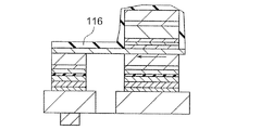
続いて、引き出し電極層18、磁性層41、金属または半導体層42、磁性層/非磁性層/磁性層からなるシンセティック構造の磁化固着層43、反強磁性層44、キャップ層45a、およびTaからなるハードマスク層45bをスパッタした。実際の膜構造は、引き出し電極層18はTa(5nm)/Ru(20nm)からなり、磁性層41はCoFe(5nm)からなり、層42はCu(2.3nm)からなり、磁化固着層43はCoFe(3.2nm)/Ru(0.9nm)/CoFe(3nm)からなり、反強磁性層44はPtMn(14nm)からなり、キャップ層45aはRu(10nm)からなり、ハードマスク層45bはTa(120nm)からなる。
Subsequently, from the
次に、レジストパターン(図示せず)を形成し、このレジストパターンをマスクとして塩素系ガスでTaからなるハードマスク層45bをRIE法を用いてエッチングし、ハードマスク45bを形成する(図51参照)。このエッチングはRuからなるキャップ層45aでストップさせた。
Next, a resist pattern (not shown) is formed, and using this resist pattern as a mask, a
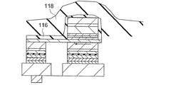
その後、レジストパターンを剥離し、Taからなるハードマスク層45bをマスクとして、Ruからなる引き出し電極18までミリングし、磁気抵抗効果素子40を形成した(図52参照)。この磁気抵抗効果素子40のサイズも、直径0.18×0.32μm2とした。
Thereafter, the resist pattern was peeled off and milled to the
次に、図53に示すように、SiOx保護膜116を成膜した後、レジストパターン(図示せず)を形成し、Ta(5nm)/Ru(20nm)からなる引き出し電極18をミリングし、レジストパターンを除去する(図54参照)。続いて、SiOxからなる層間絶縁膜118を堆積し(図55参照)、CMPおよびエッチバックを用いて層間絶縁膜118を平坦化するとともに(以降、SiOx保護膜116は図示せず)、Taからなるハードマスク層45bの表面を露出させる(図56参照)。その後、図57に示すように、ハードマスク層45bに接続するワード線30を形成する。その後、磁場中アニールを磁性層の長軸方向に磁場を印加した。
Next, as shown in FIG. 53, after forming the SiOx
図20、図21に示した書き込み/読み出し方法を用い、電流を印加し、何mAでスピンが反転するか調べたところ、0.43mAで反転し、大容量MRAMとして適した低電流でスピン注入書き込みができることが分かった。また、書き込み−読み出しサイクルを109回行い信頼性の検査を行ったが、変化は無く信頼性が確保できるメモリ構造であることが分かった。
When the current was applied and the spin was reversed by using the write / read method shown in FIGS. 20 and 21, the spin was reversed at 0.43 mA, and the spin injection was performed at a low current suitable as a large capacity MRAM. I found that I can write. The write - has been read cycles performed
(第3実施例)
本発明の第3実施例として、図23に示したアーキテクチャを有するメモリセルを作製した。この実施例のプロセス工程は、第2実施例にデジット線70を設けただけで、上記第2実施例のプロセス工程と同様である。また、膜構造,SiOx設計膜厚などの条件も同様にした。第2実施例よりもどの程度スピン注入電流が減少できるか調べた。その際、書き込み方法は、図32、図33で説明した方法を用いた。
(Third embodiment)
As a third embodiment of the present invention, a memory cell having the architecture shown in FIG. 23 was fabricated. The process steps of this embodiment are the same as the process steps of the second embodiment, except that the
電流を印加し、何mAでスピンが反転するか調べた。ワード線30に0.2mAのパルス電流を印加したところ、第3実施例は0.31mAで反転し、大容量MRAMとして適した低電流でスピン注入書き込みができることが分かった。また、書き込み−読み出しサイクルを109回行い信頼性の検査を行ったが変化は無く信頼性が確保できるメモリ構造であることが分かった。
A current was applied, and it was examined how many mA the spin was reversed. When a pulse current of 0.2 mA was applied to the
以上、具体例を参照しつつ、本発明の実施の形態について説明した。しかし、本発明は、これらの具体例に限定されるものではない。例えば、磁気抵抗効果素子を構成する強磁性体層、絶縁膜、反強磁性体層、非磁性金属層、電極などの具体的な材料や、膜厚、形状、寸法などに関しては、当業者が適宜選択することにより本発明を同様に実施し、同様の効果を得ることができるものも本発明の範囲に包含される。 The embodiments of the present invention have been described above with reference to specific examples. However, the present invention is not limited to these specific examples. For example, a person skilled in the art is concerned with specific materials, such as a ferromagnetic layer, an insulating film, an antiferromagnetic layer, a nonmagnetic metal layer, and an electrode constituting the magnetoresistive effect element, as well as a film thickness, a shape, and a dimension. Appropriate selections that similarly implement the present invention and obtain similar effects are also included in the scope of the present invention.
同様に、本発明の磁気メモリを構成する各要素の構造、材質、形状、寸法についても、当業者が適宜選択することにより本発明を同様に実施し、同様の効果を得ることができるものも本発明の範囲に包含される。 Similarly, the structure, material, shape, and dimensions of each element constituting the magnetic memory of the present invention can be appropriately selected by those skilled in the art to implement the present invention in the same manner and obtain similar effects. It is included in the scope of the present invention.
その他、本発明の実施の形態として上述した磁気メモリを基にして、当業者が適宜設計変更して実施し得るすべての磁気メモリも同様に本発明の範囲に属する。 In addition, all magnetic memories that can be implemented by those skilled in the art based on the above-described magnetic memory as an embodiment of the present invention are also within the scope of the present invention.
1 メモリセル
1A〜1G メモリセル
2 磁気抵抗効果素子
2A〜2G 磁気抵抗効果素子
4 反強磁性層
5 磁化固着層
6 磁化固着層
8 トンネルバリア層
10 磁気記録層
16 下地層
18 引き出し電極(引き出し配線)
20 ビット線
30 ワード線
32 接続部
50 接続部
52 接続プラグ
54 接続プラグ
56 接続プラグ
60 選択トランジスタ
62 ゲート
64 ドレイン
66 ソース
DESCRIPTION OF
20
Claims (11)
書き込み電流によりスピンの向きが可変の磁気記録層と、
前記第1磁化固着層と前記磁気記録層との間に設けられた第1非磁性層と、
読み出し電流用の第1配線に電気的に接続され、スピンの向きが固着された第2磁化固着層と、
前記磁気記録層の前記第1非磁性層と反対側の面の第1領域と、前記第2磁化固着層の前記第1配線に電気的に接続された面と反対側の面との間に設けられた第2非磁性層と、
を備えたメモリセルを含み、前記磁気記録層の前記第1非磁性層とは反対側の面の第2領域に、前記書き込み電流用の第2配線が電気的に接続され、前記第1磁化固着層の前記第1非磁性層と反対側の面が前記書き込み電流および前記読み出し電流用の第3配線に電気的に接続されたことを特徴とする磁気メモリ。 A first magnetization pinned layer in which the spin direction is fixed;
A magnetic recording layer whose spin direction is variable by a write current;
A first nonmagnetic layer provided between the first magnetization pinned layer and the magnetic recording layer;
A second magnetization pinned layer electrically connected to the first wiring for read current and having the spin direction fixed;
Between the first region of the surface opposite to the first nonmagnetic layer of the magnetic recording layer and the surface opposite to the surface electrically connected to the first wiring of the second magnetization pinned layer. A provided second nonmagnetic layer;
A second wiring for the write current is electrically connected to a second region of the surface of the magnetic recording layer opposite to the first nonmagnetic layer, and the first magnetization A magnetic memory, wherein a surface of the pinned layer opposite to the first nonmagnetic layer is electrically connected to the third wiring for the write current and the read current.
書き込み電流によりスピンの向きが可変の磁気記録層と、
前記第1磁化固着層と前記磁気記録層との間に設けられた第1非磁性層と、
読み出し電流および前記書き込み電流用の第1配線に電気的に接続され、スピンの向きが固着された第2磁化固着層と、
前記第2磁化固着層の前記第1配線に電気的に接続された面と反対側の面と、前記磁気記録層の前記第1非磁性層と反対側の面の第1領域との間に設けられた第2非磁性層と、
を備えたメモリセルを含み、前記磁気記録層の前記第1非磁性層とは反対側の面の第2領域に、前記書き込み電流用の第2配線が電気的に接続され、前記第1磁化固着層の前記第1非磁性層と反対側の面が前記読み出し電流用の第3配線に電気的に接続されたことを特徴とする磁気メモリ。 A first magnetization pinned layer in which the spin direction is fixed;
A magnetic recording layer whose spin direction is variable by a write current;
A first nonmagnetic layer provided between the first magnetization pinned layer and the magnetic recording layer;
A second magnetization pinned layer electrically connected to the first wiring for the read current and the write current and having the spin direction fixed;
Between the surface of the second magnetization pinned layer opposite to the surface electrically connected to the first wiring and the first region of the surface of the magnetic recording layer opposite to the first nonmagnetic layer. A provided second nonmagnetic layer;
A second wiring for the write current is electrically connected to a second region of the surface of the magnetic recording layer opposite to the first nonmagnetic layer, and the first magnetization A magnetic memory, wherein a surface of the fixed layer opposite to the first nonmagnetic layer is electrically connected to the third wiring for read current.
前記書き込み電流によりスピンの向きが可変の磁気記録層と、
前記第1磁化固着層の前記第1配線に電気的に接続された面と反対側の面と、前記磁気記録層との間に設けられた第1非磁性層と、
第1読み出し電流用の第2配線に電気的に接続され、スピンの向きが固着された第2磁化固着層と、
第2読み出し電流用の第3配線に電気的に接続され、スピンの向きが固着された第3磁化固着層と、
前記磁気記録層の前記第1非磁性層と反対側の面の第1領域と、前記第2磁化固着層の前記第2配線に電気的に接続された面と反対側の面との間に設けられた第2非磁性層と、 前記磁気記録層の前記第1非磁性層と反対側の面の第2領域と、前記第3磁化固着層の前記第3配線に電気的に接続された面と反対側の面との間に設けられた第3非磁性層と、 を備えたメモリセルを含み、
前記磁気記録層の前記第1非磁性層と反対側の面の第3領域に前記書き込み電流および前記読み出し電流用の第4配線が電気的に接続されたことを特徴とする磁気メモリ。 A first magnetization pinned layer electrically connected to the first wiring for write current and pinned in the spin direction;
A magnetic recording layer whose spin direction is variable by the write current;
A first nonmagnetic layer provided between a surface of the first magnetization pinned layer opposite to a surface electrically connected to the first wiring and the magnetic recording layer;
A second magnetization pinned layer electrically connected to the second wiring for the first read current and pinned in a spin direction;
A third magnetization pinned layer electrically connected to the third wiring for the second read current and having the spin direction fixed;
Between the first region of the surface opposite to the first nonmagnetic layer of the magnetic recording layer and the surface opposite to the surface electrically connected to the second wiring of the second magnetization pinned layer. Electrically connected to the provided second nonmagnetic layer, the second region of the surface of the magnetic recording layer opposite to the first nonmagnetic layer, and the third wiring of the third magnetization pinned layer A third nonmagnetic layer provided between the surface and the opposite surface; and a memory cell comprising:
A magnetic memory, wherein the write current and the fourth wire for the read current are electrically connected to a third region of the surface of the magnetic recording layer opposite to the first nonmagnetic layer.
前記第1配線の一方の側に電気的に接続され、スピンの向きが可変の磁気記録層と、
前記読み出し電流用の第2配線に電気的に接続され、スピンの向きが固着された第1磁化固着層と、
前記磁気記録層と前記第1磁化固着層との間に設けられた第1非磁性層と、
前記第1配線の他方の側に電気的に接続され、前記磁気記録層と反強磁性結合または静磁結合する少なくとも1層の第1磁性層と、
前記書き込み電流用の第3配線に電気的に接続され、磁化の向きが固着された第2磁化固着層と、
前記第1磁性層と前記第2磁化固着層との間に設けられた第2非磁性層と、
を備えたメモリセルを含むことを特徴とする磁気メモリ。 A first wiring for read current and write current;
A magnetic recording layer electrically connected to one side of the first wiring and having a variable spin direction;
A first magnetization pinned layer electrically connected to the second wiring for the read current and pinned in a spin direction;
A first nonmagnetic layer provided between the magnetic recording layer and the first magnetization pinned layer;
At least one first magnetic layer electrically connected to the other side of the first wiring and antiferromagnetically or magnetostatically coupled to the magnetic recording layer;
A second magnetization pinned layer electrically connected to the third wiring for write current and having a magnetization direction fixed;
A second nonmagnetic layer provided between the first magnetic layer and the second magnetization pinned layer;
A magnetic memory comprising: a memory cell comprising:
Priority Applications (1)
| Application Number | Priority Date | Filing Date | Title |
|---|---|---|---|
| JP2003350988A JP4080982B2 (en) | 2003-10-09 | 2003-10-09 | Magnetic memory |
Applications Claiming Priority (1)
| Application Number | Priority Date | Filing Date | Title |
|---|---|---|---|
| JP2003350988A JP4080982B2 (en) | 2003-10-09 | 2003-10-09 | Magnetic memory |
Publications (2)
| Publication Number | Publication Date |
|---|---|
| JP2005116888A JP2005116888A (en) | 2005-04-28 |
| JP4080982B2 true JP4080982B2 (en) | 2008-04-23 |
Family
ID=34542391
Family Applications (1)
| Application Number | Title | Priority Date | Filing Date |
|---|---|---|---|
| JP2003350988A Expired - Fee Related JP4080982B2 (en) | 2003-10-09 | 2003-10-09 | Magnetic memory |
Country Status (1)
| Country | Link |
|---|---|
| JP (1) | JP4080982B2 (en) |
Families Citing this family (30)
| Publication number | Priority date | Publication date | Assignee | Title |
|---|---|---|---|---|
| US6946697B2 (en) | 2003-12-18 | 2005-09-20 | Freescale Semiconductor, Inc. | Synthetic antiferromagnet structures for use in MTJs in MRAM technology |
| US6992359B2 (en) * | 2004-02-26 | 2006-01-31 | Grandis, Inc. | Spin transfer magnetic element with free layers having high perpendicular anisotropy and in-plane equilibrium magnetization |
| JP2007027575A (en) * | 2005-07-20 | 2007-02-01 | Toshiba Corp | Magnetoresistance effect element and magnetic memory |
| FR2889348B1 (en) * | 2005-07-27 | 2008-09-12 | Commissariat Energie Atomique | MAGNETORESISTIVE DEVICE |
| JP5591888B2 (en) * | 2005-07-28 | 2014-09-17 | 株式会社日立製作所 | Magnetoresistive element and nonvolatile magnetic memory equipped with the same |
| JP2007053143A (en) * | 2005-08-15 | 2007-03-01 | Sony Corp | Memory element and memory |
| JP2007095765A (en) * | 2005-09-27 | 2007-04-12 | Fuji Electric Holdings Co Ltd | Multiple-value recording spin injection magnetization inverting element and device using the same |
| JP5193419B2 (en) * | 2005-10-28 | 2013-05-08 | 株式会社東芝 | Spin injection magnetic random access memory and writing method thereof |
| JP2007123640A (en) * | 2005-10-28 | 2007-05-17 | Sharp Corp | Magnetic memory, information recording/reproducing method, information reproducing method and information recording method |
| JP4997789B2 (en) * | 2006-02-23 | 2012-08-08 | Tdk株式会社 | Magnetic memory |
| JP5002996B2 (en) * | 2006-03-30 | 2012-08-15 | 富士通株式会社 | Semiconductor memory device, manufacturing method thereof, data writing method thereof, and data reading method thereof |
| JP4797795B2 (en) * | 2006-05-24 | 2011-10-19 | Tdk株式会社 | Magnetic memory |
| JP5034318B2 (en) * | 2006-05-24 | 2012-09-26 | Tdk株式会社 | Magnetic memory |
| JP4518049B2 (en) * | 2006-07-03 | 2010-08-04 | ソニー株式会社 | Storage device |
| JP2008078378A (en) | 2006-09-21 | 2008-04-03 | Alps Electric Co Ltd | Tunnel-type magnetism detecting element and manufacturing method thereof |
| JP5147212B2 (en) * | 2006-10-04 | 2013-02-20 | 株式会社日立製作所 | Magnetic memory cell and magnetic random access memory |
| JP2008171862A (en) * | 2007-01-09 | 2008-07-24 | Nec Corp | Magnetoresistive effect element and mram |
| JP2009049101A (en) * | 2007-08-16 | 2009-03-05 | Sony Corp | Magnetic memory element and magnetic memory device |
| US8154913B2 (en) | 2007-10-25 | 2012-04-10 | Nec Corporation | Magnetoresistance effect element and magnetic random access memory |
| US7577021B2 (en) * | 2007-11-21 | 2009-08-18 | Magic Technologies, Inc. | Spin transfer MRAM device with separated CPP assisted writing |
| US8004881B2 (en) * | 2007-12-19 | 2011-08-23 | Qualcomm Incorporated | Magnetic tunnel junction device with separate read and write paths |
| US8149615B2 (en) | 2008-02-19 | 2012-04-03 | Nec Corporation | Magnetic random access memory |
| JP5299642B2 (en) * | 2008-02-19 | 2013-09-25 | 日本電気株式会社 | Magnetic random access memory |
| JP5435298B2 (en) * | 2008-03-07 | 2014-03-05 | 日本電気株式会社 | Semiconductor device |
| JP5175750B2 (en) | 2009-01-19 | 2013-04-03 | 株式会社日立製作所 | Manufacturing method of semiconductor integrated circuit device using magnetic memory element |
| JP5472832B2 (en) * | 2009-09-28 | 2014-04-16 | 日本電気株式会社 | Magnetic memory |
| JP5814680B2 (en) | 2011-07-29 | 2015-11-17 | 株式会社東芝 | Magnetoresistive element and magnetic memory |
| JP5809903B2 (en) * | 2011-09-21 | 2015-11-11 | 株式会社東芝 | Nonvolatile memory device |
| US8570792B2 (en) * | 2012-01-24 | 2013-10-29 | Taiwan Semiconductor Manufacturing Co., Ltd. | Magnetoresistive random access memory |
| US8884386B2 (en) | 2012-02-02 | 2014-11-11 | Taiwan Semiconductor Manufacturing Company, Ltd. | MRAM device and fabrication method thereof |
-
2003
- 2003-10-09 JP JP2003350988A patent/JP4080982B2/en not_active Expired - Fee Related
Also Published As
| Publication number | Publication date |
|---|---|
| JP2005116888A (en) | 2005-04-28 |
Similar Documents
| Publication | Publication Date | Title |
|---|---|---|
| JP4080982B2 (en) | Magnetic memory | |
| JP3824600B2 (en) | Magnetoresistive element and magnetic memory | |
| JP4504273B2 (en) | Magnetoresistive element and magnetic memory | |
| JP3863484B2 (en) | Magnetoresistive element and magnetic memory | |
| JP3873015B2 (en) | Magnetic memory | |
| JP4253225B2 (en) | Magnetoresistive element and magnetic memory | |
| JP4693450B2 (en) | Magnetoresistive element and magnetic memory | |
| JP4371781B2 (en) | Magnetic cell and magnetic memory | |
| JP4157707B2 (en) | Magnetic memory | |
| EP1320104B1 (en) | Magnetic memory device and manufacturing method thereof | |
| JP3583102B2 (en) | Magnetic switching element and magnetic memory | |
| JP4952725B2 (en) | Nonvolatile magnetic memory device | |
| JP2007027575A (en) | Magnetoresistance effect element and magnetic memory | |
| EP1349172A1 (en) | Magnetic logic element, magnetic memory element and arrays thereof | |
| JP2009094104A (en) | Magnetoresistive element | |
| JP2007299931A (en) | Magnetoresistance effect element and magnetic memory | |
| JP2006190838A (en) | Memory element and memory | |
| JP4005832B2 (en) | Magnetic memory and magnetic memory device | |
| JP4187021B2 (en) | Memory element and memory | |
| JP2007281247A (en) | Spin memory | |
| JP2003163330A (en) | Magnetic memory | |
| JP4575101B2 (en) | Magnetoresistive element and magnetic memory | |
| JP5087067B2 (en) | Magnetoresistive element and magnetic memory | |
| JP2006108316A (en) | Memory element and memory | |
| JP2006148039A (en) | Magneto-resistance effect element and magnetic memory |
Legal Events
| Date | Code | Title | Description |
|---|---|---|---|
| A621 | Written request for application examination |
Free format text: JAPANESE INTERMEDIATE CODE: A621 Effective date: 20050203 |
|
| A977 | Report on retrieval |
Free format text: JAPANESE INTERMEDIATE CODE: A971007 Effective date: 20071212 |
|
| A131 | Notification of reasons for refusal |
Free format text: JAPANESE INTERMEDIATE CODE: A131 Effective date: 20071218 |
|
| A521 | Request for written amendment filed |
Free format text: JAPANESE INTERMEDIATE CODE: A523 Effective date: 20080110 |
|
| TRDD | Decision of grant or rejection written | ||
| A01 | Written decision to grant a patent or to grant a registration (utility model) |
Free format text: JAPANESE INTERMEDIATE CODE: A01 Effective date: 20080201 |
|
| A61 | First payment of annual fees (during grant procedure) |
Free format text: JAPANESE INTERMEDIATE CODE: A61 Effective date: 20080207 |
|
| FPAY | Renewal fee payment (event date is renewal date of database) |
Free format text: PAYMENT UNTIL: 20110215 Year of fee payment: 3 |
|
| FPAY | Renewal fee payment (event date is renewal date of database) |
Free format text: PAYMENT UNTIL: 20110215 Year of fee payment: 3 |
|
| FPAY | Renewal fee payment (event date is renewal date of database) |
Free format text: PAYMENT UNTIL: 20120215 Year of fee payment: 4 |
|
| FPAY | Renewal fee payment (event date is renewal date of database) |
Free format text: PAYMENT UNTIL: 20120215 Year of fee payment: 4 |
|
| FPAY | Renewal fee payment (event date is renewal date of database) |
Free format text: PAYMENT UNTIL: 20130215 Year of fee payment: 5 |
|
| FPAY | Renewal fee payment (event date is renewal date of database) |
Free format text: PAYMENT UNTIL: 20140215 Year of fee payment: 6 |
|
| LAPS | Cancellation because of no payment of annual fees |