JP4079397B2 - Tracking mechanism and tracking method for recording / reproducing apparatus - Google Patents
Tracking mechanism and tracking method for recording / reproducing apparatus Download PDFInfo
- Publication number
- JP4079397B2 JP4079397B2 JP21859298A JP21859298A JP4079397B2 JP 4079397 B2 JP4079397 B2 JP 4079397B2 JP 21859298 A JP21859298 A JP 21859298A JP 21859298 A JP21859298 A JP 21859298A JP 4079397 B2 JP4079397 B2 JP 4079397B2
- Authority
- JP
- Japan
- Prior art keywords
- tracking
- recording medium
- probe
- recording
- probes
- Prior art date
- Legal status (The legal status is an assumption and is not a legal conclusion. Google has not performed a legal analysis and makes no representation as to the accuracy of the status listed.)
- Expired - Fee Related
Links
Images


Landscapes
- Length Measuring Devices With Unspecified Measuring Means (AREA)
Description
【0001】
【発明の属する技術分野】
本発明は記録再生装置のトラッキング機構及びトラッキング方法に関し、例えばSTMの原理を用いて高密度・大容量メモリ装置を構成する際のトラッキング機構及びトラッキング方法に関するものである。
【0002】
【従来の技術】
近年、導体の電子構造を直接観察できる走査型トンネル顕微鏡(以後、STMと略す)が開発され[G.Binning et al.Phys.Rev.Lett,49,57(1982)]、単結晶、多結晶を問わず実空間像の高い分解能の測定ができるようになった。
以来、先端の尖ったプローブを走査することにより様々な情報を得る走査プローブ顕微鏡(SPM)や、さらに基板に電気的、化学的あるいは物理的作用を及ぼす事を目的としたSPMを応用した微細加工技術の研究開発が行われている。さらに、このようなSPM技術はメモリ技術にも応用されつつある。例えば、特開昭63−161552号公報、特開昭63−161553号公報等には、記録層として電圧電流のスイッチング特性に対してメモリ効果を持つ材料、例えばπ電子径有機化合物やカルコゲン化合物類の薄膜層を用いて、記録・再生をSPMで行う方法が開示されている。この方法を用いて記録のビットサイズを直径10[nm]とすれば、1012bit/cm2の記録密度を持つ情報処理装置が実現できる。
【0003】
さて、一般に媒体上に記録された情報を読み出す場合には、媒体上の情報列に沿って情報読み出し用のプローブを相対移動させる必要がある。
まず、情報列の位置を検出する方法として媒体上に物理的なトラックを形成し、そのトラックにプローブを沿わせる方法が知られている。
特開平1−107341号公報には記録媒体表面にトラックとしてV字型の溝を形成し、プローブ電極が常にこの溝の中央に位置するように制御する方法が開示されている。
また特開平1−133239号公報には記録媒体の下にトラックを導電体層で形成して、トラックにトラッキング信号を印加し、プローブから検出されるトラッキング信号に基づいてフィードバック制御を行う方法が開示されている。
【0004】
【発明が解決しようとする課題】
しかしながら、特開平1−107341号公報や特開平1−133239号公報に開示されているような媒体上に物理トラックを作成する方法は、物理トラックを設ける工程が必要になる。したがって、記録媒体の作成工程が複雑になることや、物理的な加工を行うために、記録媒体や、その基板の材質に対する制限が問題となる。
【0005】
そこで、本発明は上記した従来のものにおける課題を解決し、記録媒体に物理的な加工を行うことなく、記録再生と共通の原理を用いて、ビット列を利用して高精度な制御が可能なトラッキングを行い、エラーがなく安定した情報の記録及び再生のできる記録再生装置のトラッキング機構及びトラッキング方法を提供することを目的とする。
【0006】
【課題を解決するための手段】
本発明は、上記課題を達成するため、記録再生装置のトラッキング機構及びトラッキング方法を、つぎのように構成したことを目的としている。
すなわち、本発明のトラッキング機構は、記録媒体に対しプローブを相対走査してトラッキングを行いながら前記記録媒体上に情報を記録し、前記記録媒体上に記録された情報を再生する記録再生装置のトラッキング機構であって、
前記記録媒体上を走査して該記録媒体上にトラッキングビット列を記録すると共に、該トラッキングビット列を再生するように走査する際に用いられる、一体成形された2本1組のトラッキングプローブと、
前記2本1組のトラッキングプローブの前記記録媒体の表面と平行な面内における角度を変化させることで、該2本1組のトラッキングプローブの見かけの間隔を変化させる角度制御手段と、
前記記録媒体上に形成された該トラッキングプローブに対応する2本1組のトラッキングビット列を再生するように走査する手段と、
前記走査による再生出力に応じて制御信号出力手段から制御信号を出力し、該制御信号に基づいて前記記録媒体とプローブとの相対位置を制御する制御信号出力手段と、
を有することを特徴としている。
また、本発明のトラッキング機構は、前記制御信号出力手段が、前記2本のトラッキングプローブからの出力を比較し、比較結果に応じた符合と絶対値を持つ信号を出力する比較演算手段であることを特徴としている。
また、本発明のトラッキング機構は、前記制御信号出力手段が、前記2本1組のトラッキングプローブからの再生出力を保持するホールド手段と、該再生出力がしきい値を超えた時に該ホールド手段をリセットするしきい値検出手段と、を有することを特徴としている。
また、本発明のトラッキング機構は、前記制御信号出力手段が、前記2本1組のトラッキングプローブからの再生出力を2値化する2値化回路を有することを特徴としている。
また、本発明のトラッキング機構は、前記制御信号出力手段が、過去の信号の履歴を積分する積分手段と、該積分手段からの信号を増幅して制御信号として出力する増幅手段と、を有することを特徴としている。
【0007】
また、本発明のトラッキング方法は、記録媒体上を記録再生プローブで相対走査して該記録媒体上に情報を記録再生する記録再生装置のトラッキング方法であって、
一体成形された2本1組のトラッキングプローブで該記録媒体上を走査して該記録媒体上にトラッキングビット列を記録し、
該2本1組のトラッキングプローブの該記録媒体の表面と平行な面内における角度を変化させることで該2本1組のトラッキングプローブの見かけの間隔を変化させ、
該2本1組のトラッキングプローブにより記録されたトラッキングビット列を再生するように、該2本1組のトラッキングプローブで該記録媒体上を走査し、
該トラッキングビット列の再生出力に応じて制御信号を出力し、該制御信号に基づいて該記録媒体と前記プローブとの相対位置を制御しながら、該記録再生プローブで該記録媒体上を走査し情報を記録再生することを特徴としている。
【0008】
【発明の実施の形態】
本発明は、上記した構成により、記録媒体に形成されたビット列を利用して、前記記録媒体とプローブとの相対位置を高精度に制御しながらトラッキングを行うことができるため、従来のように記録媒体に物理トラックを作成するための物理的な加工を行う必要がなく、エラーの少ない安定した情報の記録及び再生が可能となる。
すなわち、本発明においては、トラッキングビット列を、例えば、2本1組のトラッキングプローブで生成し、この2本1組のトラッキングプローブを一体として記録媒体表面と平行な面内において角度を変化させることでトラッキングプローブの見かけの間隔を変化させ、この状態でトラッキングビット列の再生動作を行い、トラッキングプローブによるトラッキングビット列の再生信号を比較することにより、データの記録再生と同じ方法によって高精度で、高速で安定したトラッキングが可能となる。
また、直前のトラッキングビットの再生信号をホールドすることにより、トラッキングビット列間のビット再生タイミングのずれへの対応や、トラッキングビット列を用いたアドレス情報やその他のデータの記録再生が可能となる。
【0009】
以下、図面を参照しながら本発明の実施の形態について説明する。
まず、間隔dで並んだ2本のトラッキングプローブ101、102を用いて、トラッキングのために2列のトラッキングビット列を形成する。この後、図1に示すように2本のトラッキングプローブとトラッキングビット列の相対角度をθ変化させる。これによって、先に形成したトラッキングビット列の間隔に対する、トラッキングプローブの見かけの間隔が変化する。図1は、見かけのプローブ間隔をΔdだけ狭くした場合の例である。もちろん、見かけのプローブ間隔をΔdだけ広くしてもかまわない。
ここで、2本のトラッキングプローブで、記録媒体上をトラッキングビット列に対して平行な方向(矢印の方向)にバイアス電圧を印加した状態で走査すると、プローブがトラッキングビット103上を通過する際にプローブと記録媒体との間に電流が流れる。ここで図2に示す比較回路204を用いて2本のプローブによるトラッキングビット103の再生出力の比較を行う。
【0010】
図3に示すように、トラッキングプローブが目標通りの位置にある場合には、比較回路204からのエラー信号は出力されない。しかし、図4、図5に示すようにトラッキングビット列に対して垂直方向に誤差が生じた場合、誤差の向きに応じた極性と誤差量に応じた絶対値を持つエラー信号が比較回路204から出力される。これを用いてxy駆動ステージ608を制御する。
さらに、トラッキングビット列にアドレス情報やその他のデータを記録することも可能である。
また、間隔制御のための角度変化によって、2本のトラッキングプローブの間で記録再生走査方向の位置が大きくずれた場合、あるいは、2本のトラッキングプローブで別々のデータをトラッキングビット列として記録した場合は、一方のプローブのみがトラッキングビット103を再生する場合がある。このような場合には、直前のトラッキングビット103の再生信号を保持し、次のトラッキングビットが出現するまでの間、これを用いてトラッキングを行う機構を用いることで対処できる。
【0011】
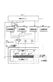
本発明を適用する記録再生装置は前記記録再生装置に限られるものではない。磁気記録再生装置、光磁気記録再生装置、近接場光記録再生装置等、他の記録再生装置にも適用可能であるが、以下に、図6を用いて、本発明を記録再生装置に適用した例の概要を説明する。
導電性を有する基板601上の記録層602からなる記録媒体603に対し、先端に設けられている探針604が接触するように、複数のプローブ605が配置されている。各プローブ605において、探針604は、たわむ様に弾性変形を生じる弾性体606により支持されている。
ここで、弾性体606の弾性変形の弾性定数が約0.1[N/m]、弾性変形量が約1[μm]であるとすると、記録媒体に対する探針の接触力は約10-7[N]程度となる。
【0012】
制御コンピュータ614により制御された位置制御回路613からの位置制御信号を受け、記録媒体603に取り付けられたxy駆動ステージ608が駆動され、プローブ605と記録媒体603とは記録媒体603に平行な面内において相対的に2次元方向に移動する。記録媒体603に対し、プローブの605のxy方向位置を調節し、探針604先端が記録媒体603上の所望の位置になるようプローブ605が位置合わせされる。
上記の記録再生装置において記録媒体603に対しプローブ605を走査する際、プローブ605上の探針604先端は記録媒体603に対し、常に接触した状態を保つ。
【0013】
このような接触走査方式は、探針604先端を記録媒体603に対し接触させたまま走査する場合に、記録媒体603の表面に凹凸があっても、弾性体606の弾性変形によりこれを吸収するため、探針604先端と記録媒体603表面の接触力はほぼ一定に保たれ、探針604先端や記録媒体603表面が破壊することを避けられる。この方式は個々のプローブをz方向に位置合わせするピエゾ素子等の手段が不必要であるため、構成が複雑にならず、特に複数のプローブを有する装置に適している。
【0014】
また、記録媒体603に対する個々のプローブ605のz方向位置のフィードバック制御が不必要であるため、記録媒体603に対するプローブ605の高速走査が可能となる。
制御コンピュータ614により制御された角度制御回路615からの角度制御信号を受け、プローブ605に取り付けられたθ駆動ステージ607が駆動され、プローブ605と記録媒体603とのなす角度は、記録媒体603の表面と平行な面内において相対的に変化する。
制御コンピュータ614により制御された記録制御回路611から発生された記録信号が、記録系に切り替えられた切り替えスイッチ609を通し、各探針604から記録媒体603に印加される。このようにして、記録層602の探針604先端が接触する部分に局所的に記録が行われる。
【0015】
上述の装置における記録層602としては、電圧印加により流れる電流値が変化するような材料を用いる。
具体例としては、第1に、特開昭63−161552号公報、特開昭63−161553号公報に開示されているようなポリイミドやSOAZ(ビス−n−オクチルスクアリリウムアズレン)等電気メモリー効果を有するLB膜(=Langmuir−Blodgette法により作成された有機単分子の膜の累積膜)が挙げられる。この材料は、探針−LB膜−基板間にしきい値以上の電圧(5〜10[V]程度)を印加すると間のLB膜の導電性が変化(OFF状態→ON状態)し、再生用のバイアス電圧(0.01〜2[V]程度)を印加した際に流れる電流が増大するものである。
第2の具体例として、GeTe,GaSb,SnTe等の非晶質薄膜材料が挙げられる。この材料は、探針−非晶質薄膜材料−基板間に電圧を印加し、流れる電流により発生する熱で非晶質→晶質への相転移を起こさせるものである。これにより材料の導電性が変化し、再生用のバイアス電圧を印加した際に流れる電流が増大するものである。
第3の具体例として、ZnやW、Si、GaAs等の酸化性金属・半導体材料が挙げられる。この材料は、探針−酸化性金属・半導体材料間に電圧を印加すると、流れる電流により、材料表面に吸着している水や大気中の酸素と反応し、表面に酸化膜が形成される。このため材料表面の接触抵抗が変化し、バイアス電圧を印加した際に流れる電流が減少する。
【0016】
さて、上述のように記録が行われたビットの再生は次のように行う。スイッチ609により、各プローブ605からの信号配線を再生系に切り替えた後、バイアス電圧印加手段610により、探針604と基板601との間にバイアス電圧を印加し、両者の間に流れる電流を再生制御回路612において検出する。記録媒体603上の記録ビットの部分は記録がなされていない部分に比べ電流が多く(または、少なく)流れるため、再生制御回路612において、この電流の違いを検出し、再生信号とし、制御コンピュータ614に出力する。
【0017】
【実施例】
以下に、本発明の実施例について説明する。
[実施例1]
以下、図面を参照しながら、前記構成の記録再生装置に対し、本発明のトラッキング機構を適用した実施例1について詳細な説明を行う。
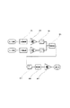
まず、上記装置に対して、図7に示すような、100[μm]間隔で一体成形された64本のプローブからなるプローブアレイ765を取り付けた。これら64本のプローブのうち、32、33番目の記録再生プローブ732、733をそれぞれトラッキングプローブ101、102として使用し、残りの62本を記録再生プローブとして使用する。この状態で、トラッキングプローブ102の探針先端からトラッキングプローブ101の探針先端を見る向きをyの正方向とし、記録媒体603の表面に垂直にプローブアレイ765から記録媒体603を見て、反時計周りをθの正の回転方向とし、yの正方向をθの負方向にπ/2[rad]回転した向きをxの正方向とする。
【0018】
次に、プローブアレイ765で、長さ110[μm]にわたり、線速度0.1[mm/s]で図1中xの正方向に、直線状に走査を行った。走査中、トラッキングプローブ102の第1の電圧パルス印加位置をトラッキングプローブ101の第1の電圧パルス印加位置に対して、走査方向に900[nm]ずらして、走査方向について50[nm]間隔で、2本のプローブそれぞれにつき、基板601との間に2048回電圧パルスを印加した。電圧は5.5V、印加時間は0.3[μsec]である。生成されたトラッキングビットの直径は約10[nm]であった。
次に、プローブアレイ765を図1中xの負方向に110[μm]、図1中yの正方向に100[nm]移動させてから、同様に、トラッキングビットの生成動作を行った。これを繰り返して各トラッキングプローブについて、図1中y方向に100[nm]間隔で10列のトラッキングビット列を生成した。
【0019】
次に、プローブアレイ765を元の位置に戻し、プローブアレイ765を記録媒体603に対して、記録媒体603の表面と平行な平面内において、トラッキングプローブ101の探針先端を中心として、θの正方向に0.009[rad]回転させた。これにより、2本のトラッキングプローブの図1中y方向の間隔は4[nm]小さくなり、トラッキングプローブ102の探針先端は、トラッキングプローブ101の探針先端に対して、図1中xの正方向に、900[nm]ずれた事になり、走査中、2本のプローブは同時にトラッキングビット103上を通過する事になる。
次に、トラッキングプローブ101、102を用いてトラッキングを行いながら、残りの62本の記録再生プローブを用いて、データビット列の記録動作を行った。
【0020】
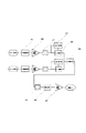
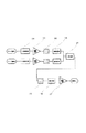
ここで、図2を用いて本実施例で用いたトラッキング機構について説明する。2本のトラッキングプローブから出力されたトラッキングビット再生時の電流信号はI/V変換回路201によって電圧信号に変換され、増幅回路202によってそれぞれ増幅された後、ローパスフィルタ203を通って、比較回路204へ入力される。比較回路204は入力された信号を比較し、その差分に応じた極性、絶対値を持つ電圧信号を出力する。この電圧信号はPIDフィルタ205を通り、積分回路206で過去の履歴と足し合わされ、増幅回路207で増幅された後、位置制御信号と足し合わされて、図6におけるxy駆動ステージ608を制御する。
トラッキングプローブ101、102と基板601との間に1.5Vのバイアス電圧を印加し、線速度2[mm/s]で、上記トラッキング機構を用いてトラッキングを行いながら長さ100[μm]にわたって、図1中のxの正方向に走査を行った。走査中、残りの記録再生プローブを用いて、基板601との間に、あらかじめ用意したデータ列に合わせて、各プローブ最大2048回電圧パルスを印加した。電圧は5.5V、印加時間は0.3[μsec]である。生成されたデータビットの直径は約10[nm]、ビット間隔は約50[nm]であった。次に、プローブアレイ765を図1中xの負方向に100[μm]、図1中yの正方向に100[nm]移動させてから、同様に走査を行い、記録動作を行った。この動作を繰り返し、各記録再生プローブについて10列のデータビット列を生成した。また、走査中にトラッキングプローブ101、102のトラッキングビット再生信号をモニタした結果、再生エラーは認められなかった。
【0021】
次に、トラッキングを行いながらデータビットの再生動作を行った。プローブアレイ765を元の位置に戻してから、プローブアレイ765の全プローブに1.5Vのバイアス電圧を印加し、線速度2[mm/s]で、トラッキングプローブ101、102で上記トラッキング機構を用いてトラッキングを行いながら走査を行った。走査中、全記録再生プローブからの再生信号をモニタした。全データビットについて50回の再生動作を行った結果、再生エラーは認められなかった。また、走査中にトラッキングプローブ101、102のトラッキングビット再生信号をモニタした結果、再生エラーは認められなかった。
【0022】
[実施例2]
以下、図面を参照しながら、前記構成の記録再生装置に対し、本発明のトラッキング機構を適用した実施例2について詳細な説明を行う。
まず、上記装置に対して、図7に示すような、100[μm]間隔で一体成形された64本のプローブからなるプローブアレイ765を取り付けた。これら64本のプローブのうち、32、33番目の記録再生プローブ732、733をそれぞれトラッキングプローブ101、102として使用し、残りの62本を記録再生プローブとして使用する。この状態で、記録媒体603の表面に垂直にプローブアレイ765から記録媒体603を見て、反時計周りをθの正の回転方向とし、トラッキングプローブ102の探針先端からトラッキングプローブ101の探針先端を見る向きをθの負方向にπ/6[rad]回転した向きをyの正方向とし、yの正方向をθの負方向にπ/2[rad]回転した向きをxの正方向とする。
【0023】
次に、プローブアレイ765を記録媒体603に対して、記録媒体603の表面と平行な平面内において、トラッキングプローブ101の探針先端を中心として、θの正方向に0.0001[rad]回転させてから、プローブアレイ765で、長さ100[μm]にわたり、線速度0.1[mm/s]で図8中xの正方向に、直線状に走査を行った。走査中、トラッキングプローブ101、102を用いて、走査方向について50[nm]間隔で、あらかじめ用意した2種類のデータにあわせて、2本のプローブそれぞれにつき、基板601との間に最大2048回電圧パルスを印加した。電圧は5.5V、印加時間は0.3[μsec]である。生成されたトラッキングビットの直径は約10[nm]であった。
【0024】
次に、プローブアレイ765を図8中xの負方向に100[μm]、図8中yの正方向に100[nm]移動させてから、同様に、トラッキングビットの生成動作を行った。これを繰り返して各トラッキングプローブについて、100[nm]間隔で10列のトラッキングビット列を生成した。
次に、プローブアレイ765を元の位置と角度に戻した。これにより、2本のトラッキングプローブの図8中y方向の間隔は5[nm]大きくなり、x方向の間隔は8.6[nm]小さくなったことになる。
次に、トラッキングプローブ101、102を用いてトラッキングを行いながら、残りの62本の記録再生プローブを用いて、データビット列の記録動作を行った。
【0025】
ここで、図9を用いて本実施例で用いたトラッキング機構について説明する。2本のトラッキングプローブから出力されたトラッキングビット再生時の電流信号はI/V変換回路201によって電圧信号に変換され、増幅回路202によってそれぞれ増幅され、ローパスフィルタ203を通った後、しきい値回路901とピークホールド回路(P/H回路)902へ入力される。しきい値回路901は、信号電圧があらかじめ定められた電圧値を超えたときにピークホールド回路(P/H回路)902に対してリセット信号を出力する。ピークホールド回路(P/H回路)902は入力された電圧の最大値を比較回路204へ出力する。本実施例においては、2本のトラッキングプローブからの信号の入力タイミングがずれる、あるいは、トラッキングビットに抜けがあるような場合、常に直前の再生信号の最大値がホールドされているため、これをトラッキングに用いる。比較回路204は、入力された信号を比較し、その差分に応じた極性と絶対値を持つ電圧信号を出力する。これにより、2つのピークホールド回路が最後にホールドした信号の差分を持つ電圧信号が得られる。この電圧信号はPIDフィルタ205を通り、積分回路206で過去の履歴と足し合わされ、増幅回路207で増幅された後、位置制御信号と足し合わされて、図6におけるxy駆動ステージ608を制御する。
【0026】
トラッキングプローブ101、102と基板601との間に1.5Vのバイアス電圧を印加し、線速度2[mm/s]で、上記トラッキング機構を用いてトラッキングを行いながら長さ100[μm]にわたって、図8中xの正方向に走査を行った。走査中、残りの記録再生プローブを用いて、基板601との間に、あらかじめ用意したデータ列に合わせて、各プローブ最大2048回電圧パルスを印加した。電圧は5.5V、印加時間は0.3[μsec]である。生成されたデータビットの直径は約10[nm]、ビット間隔は約50[nm]であった。次に、プローブアレイ765を図8中xの負方向に100[μm]、図8中yの正方向に100[nm]移動させてから、同様に走査を行い、記録動作を行った。この動作を繰り返し、各記録再生プローブについて10列のデータビット列を生成した。また、走査中にトラッキングプローブ101、102のトラッキングビット再生信号をモニタした結果、再生エラーは認められなかった。
【0027】
次に、トラッキングを行いながらデータビットの再生動作を行った。プローブアレイ765を元の位置に戻してから、プローブアレイ765の全プローブに1.5Vのバイアス電圧を印加し、線速度2[mm/s]で、トラッキングプローブ101、102で上記トラッキング機構を用いてトラッキングを行いながら走査を行った。走査中、全記録再生プローブからの再生信号をモニタした。全データビットについて50回の再生動作を行った結果、再生エラーは認められなかった。また、走査中にトラッキングプローブ101、102のトラッキングビット再生信号をモニタした結果、再生エラーは認められなかった。
さらに、トラッキングビット列生成時に用いるデータとして、アドレス情報を示すデータを用いたところ同様の結果を得た。また、この場合、記録再生動作時に、トラッキングプローブ101、102からの再生信号をモニタしたところ、各時点でのアドレス情報を得る事ができた。
【0028】
[実施例3]
以下、図面を参照しながら、前記構成の記録再生装置に対し、本発明のトラッキング機構を適用した実施例3について詳細な説明を行う。
まず、上記装置に対して、図7に示すような、100[μm]間隔で一体成形された64本のプローブからなるプローブアレイ765を取り付けた。これら64本のプローブのうち、32、33番目の記録再生プローブ732、733をそれぞれトラッキングプローブ101、102として使用し、残りの62本を記録再生プローブとして使用する。この状態で、トラッキングプローブ102の探針先端からトラッキングプローブ101の探針先端を見る向きをyの正方向とし、記録媒体603の表面に垂直にプローブアレイ765から記録媒体603を見て、反時計周りをθの正の回転方向とし、yの正方向をθの負方向にπ/2[rad]回転した向きをxの正方向とする。
【0029】
次に、プローブアレイ765で、長さ80[μm]にわたり、線速度0.1[mm/s]で図10中yの正方向に、直線状に走査を行った。走査中、トラッキングプローブ101、102を用いて、走査方向について40[nm]間隔で、あらかじめ用意したアドレス情報を示す同じデータにあわせて、2本のトラッキングプローブに同時に、基板601との間に最大2048回電圧パルスを印加した。電圧は5.5V、印加時間は0.3[μsec]である。生成されたトラッキングビットの直径は約10[nm]であった。
次に、プローブアレイ765を図10中yの負方向に80[μm]、図10中xの正方向に100[nm]移動させてから、同様に、トラッキングビットの生成動作を行った。これを繰り返して各トラッキングプローブについて、100[nm]間隔で10列のトラッキングビット列を生成した。
【0030】
次に、プローブアレイ765を元の位置に戻し、プローブアレイ765を記録媒体603に対して、記録媒体603と平行な平面内において、トラッキングプローブ101の探針先端を中心として、θの正方向に0.00005[rad]回転させた。これにより、2本のトラッキングプローブの図10中x方向の間隔は5[nm]大きくなり、図10中y方向の間隔は0.000125[nm]大きくなった事になる。y方向の間隔の変化はトラッキングビット103の直径10[nm]に対して十分に小さいため、無視できる。
次に、トラッキングプローブ101、102を用いてトラッキングを行いながら、残りの62本の記録再生プローブを用いて、データビット列の記録動作を行った。
【0031】
ここで、図11を用いて本実施例で用いたトラッキング機構について説明する。2本のトラッキングプローブから出力されたトラッキングビット再生時の電流信号はI/V変換回路201によって電圧信号に変換され、増幅回路202によってそれぞれ増幅された後、ローパスフィルタ203を通って、2値化回路1101で2値化を行った後、比較回路204へ入力される。比較回路204は入力された信号を比較し、その差分に応じた極性を持つ定電圧信号を出力する。これにより、2つの信号の長さの差分だけの長さを持った定電圧パルスが得られる事になる。この電圧信号はPIDフィルタ205を通り、積分回路206で過去の履歴と足し合わされ、増幅回路207で増幅された後、位置制御信号と足し合わされて、図6におけるxy駆動ステージ608を制御する。
【0032】
トラッキングプローブ101、102と基板601との間に1.5Vのバイアス電圧を印加し、線速度2[mm/s]で、上記トラッキング機構を用いてトラッキングを行いながら長さ80[μm]にわたって、図10中yの正方向に走査を行った。走査中、残りの記録再生プローブを用いて、基板601との間に、あらかじめ用意したデータ列に合わせて、各プローブ最大2048回電圧パルスを印加した。電圧は5.5V、印加時間は0.3[μsec]である。生成されたデータビットの直径は約10[nm]、ビット間隔は約40[nm]であった。次に、プローブアレイ765を図10中yの負方向に80[μm]、xの正方向に100[nm]移動させてから、同様に走査を行い、記録動作を行った。この動作を繰り返し、各記録再生プローブについて10列のデータビット列を生成した。また、走査中にトラッキングプローブ101、102のトラッキングビット再生信号をモニタし、アドレス情報を得た。
【0033】
次に、トラッキングを行いながらデータビットの再生動作を行った。プローブアレイ765を元の位置に戻してから、プローブアレイ765の全プローブに1.5Vのバイアス電圧を印加し、線速度2[mm/s]で、トラッキングプローブ101、102で上記トラッキング機構を用いてトラッキングを行いながら走査を行った。走査中、全記録再生プローブからの再生信号をモニタし、アドレス情報を得た。全データビットについて50回の再生動作を行った結果、再生エラーは認められなかった。
【0034】
【発明の効果】
以上説明したように、本発明によれば、一体成形された2本1組のトラッキングプローブの見かけの間隔を変化させて、該記録媒体上に形成された該トラッキングプローブに対応する2本1組のトラッキングビット列を再生するように走査し、該走査による再生出力に応じて制御信号を出力し、該制御信号に基づいて前記記録媒体とプローブとの相対位置を制御しながらトラッキングを行うように構成されているから、記録媒体に形成されたビット列を利用して、前記記録媒体とプローブとの相対位置を高精度に制御しながらトラッキングを行うことができ、従来のように記録媒体に物理トラックを作成するための物理的な加工を行う必要がなく、上記2本1組のトラッキングプローブによりエラーの少ない安定した情報の記録及び再生が可能となる。
また、本発明においては、直前のトラッキングビットの再生信号をホールドするように構成することにより、トラッキングビット列間のビット再生タイミングのずれへの対応や、トラッキングビット列を用いたアドレス情報やその他のデータの記録再生が可能となる。
また、本発明においては、トラッキングビット列にアドレス情報やその他のデータを記録し、トラッキングプローブによりそれらを再生できるようにすることができる。
【図面の簡単な説明】
【図1】本発明の実施例1を説明する図である。
【図2】本発明の実施例1のトラッキング機構を説明する図である。
【図3】本発明のトラッキング機構の原理を説明する図である。
【図4】本発明のトラッキング機構の原理を説明する図である。
【図5】本発明のトラッキング機構の原理を説明する図である。
【図6】本発明を適用する記録再生装置の全体構成を説明する図である。
【図7】本発明の実施例で用いたプローブアレイの構成を説明する図である。
【図8】本発明の実施例2を説明する図である。
【図9】本発明の実施例2のトラッキング機構を説明する図である。
【図10】本発明の実施例3を説明する図である。
【図11】本発明の実施例3のトラッキング機構を説明する図である。
【符号の説明】
101:トラッキングプローブ
102:トラッキングプローブ
103:トラッキングビット
201:I/V変換回路
202:増幅回路
203:ローパスフィルタ
204:比較回路
205:PIDフィルタ
206:積分回路
207:増幅回路
601:基板
602:記録層
603:記録媒体
604:探針
605:プローブ
606:弾性体
607:θ駆動ステージ
608:xy駆動ステージ
609:切り替えスイッチ
610:バイアス印加手段
611:記録制御回路
612:再生制御回路
613:位置制御回路
614:制御コンピュータ
615:角度制御回路
701:プローブ
702:プローブ
703:プローブ
732:プローブ
733:プローブ
763:プローブ
764:プローブ
765:プローブアレイ
901:しきい値回路
902:ピークホールド回路
1101:2値化回路[0001]
BACKGROUND OF THE INVENTION
The present invention relates to a tracking mechanism and a tracking method of a recording / reproducing apparatus, for example, a tracking mechanism and a tracking method when a high-density and large-capacity memory device is configured using the principle of STM.
[0002]
[Prior art]
In recent years, a scanning tunneling microscope (hereinafter abbreviated as STM) capable of directly observing the electronic structure of a conductor has been developed [G. Binning et al. Phys. Rev. Lett, 49, 57 (1982)], it has become possible to measure a real space image with high resolution regardless of single crystal or polycrystal.
Since then, scanning probe microscope (SPM), which obtains various information by scanning a probe with a sharp tip, and fine processing using SPM for the purpose of exerting electrical, chemical or physical action on the substrate. Technology research and development is underway. Furthermore, such SPM technology is being applied to memory technology. For example, Japanese Patent Laid-Open Nos. 63-161552 and 63-161553 disclose materials having a memory effect with respect to voltage-current switching characteristics as recording layers, such as π electron diameter organic compounds and chalcogen compounds. A method of performing recording / reproduction by SPM using a thin film layer is disclosed. If the bit size of recording is 10 [nm] using this method, 1012bit / cm2An information processing apparatus having a recording density of can be realized.
[0003]
In general, when reading information recorded on a medium, it is necessary to relatively move an information reading probe along an information string on the medium.
First, as a method for detecting the position of an information string, a method is known in which a physical track is formed on a medium and a probe is placed along the track.
Japanese Patent Laid-Open No. 1-107341 discloses a method of forming a V-shaped groove as a track on the surface of a recording medium and controlling the probe electrode so that it is always located at the center of the groove.
Japanese Laid-Open Patent Publication No. 1-133239 discloses a method in which a track is formed of a conductive layer under a recording medium, a tracking signal is applied to the track, and feedback control is performed based on the tracking signal detected from the probe. Has been.
[0004]
[Problems to be solved by the invention]
However, the method of creating a physical track on a medium as disclosed in Japanese Patent Application Laid-Open Nos. 1-107341 and 1-133239 requires a step of providing a physical track. Therefore, the production process of the recording medium becomes complicated, and restrictions on the material of the recording medium and its substrate become a problem in order to perform physical processing.
[0005]
Therefore, the present invention solves the above-described problems in the conventional apparatus, and enables high-precision control using a bit string using a principle common to recording and reproduction without performing physical processing on the recording medium. It is an object of the present invention to provide a tracking mechanism and a tracking method of a recording / reproducing apparatus capable of performing tracking and recording and reproducing information stably without error.
[0006]
[Means for Solving the Problems]
In order to achieve the above object, an object of the present invention is to configure a tracking mechanism and a tracking method of a recording / reproducing apparatus as follows.
That is, the tracking mechanism of the present invention records information on the recording medium while performing tracking by scanning the probe relative to the recording medium.,in frontA recording / playback device tracking mechanism for playing back information recorded on a recording medium,
The recording bit is recorded on the recording medium by scanning the recording medium, and is integrally formed for use in scanning to reproduce the tracking bit string.Two pairs of tracking probesWhen,
SaidBy changing the angle of a set of two tracking probes in a plane parallel to the surface of the recording medium,Changing the apparent interval between the two pairs of tracking probesAngle control means;
SaidScanning to reproduce a set of two tracking bit strings corresponding to the tracking probe formed on the recording mediumMeans to
SaidA control signal is output from the control signal output means in accordance with the reproduction output by scanning, and the relative position between the recording medium and the probe based on the control signalControlControlControl signal output means;
HaveIt is characterized by that.
In the tracking mechanism of the present invention, the control signal output means compares the outputs from the two tracking probes and outputs a signal having a sign and an absolute value according to the comparison result. It is characterized by.
In the tracking mechanism of the present invention, the control signal output means includes a holding means for holding the reproduction output from the pair of tracking probes, and the holding means when the reproduction output exceeds a threshold value. And a threshold value detecting means for resetting.
Further, the tracking mechanism of the present invention is characterized in that the control signal output means has a binarization circuit for binarizing the reproduction output from the pair of tracking probes.
In the tracking mechanism of the present invention, the control signal output means includes integration means for integrating past signal histories, and amplification means for amplifying the signal from the integration means and outputting the amplified signal as a control signal. It is characterized by.
[0007]
In addition, the tracking method of the present invention performs recording on a recording medium.Recording / playbackA recording / reproducing apparatus tracking method for recording / reproducing information on / from the recording medium by performing relative scanning with a probe,
Integrally moldedTwo pairs of tracking probesTo scan the recording medium and record a tracking bit string on the recording medium,
This set of two tracking probesTheBy changing the angle in a plane parallel to the surface of the recording medium, the apparent distance between the two pairs of tracking probes can be changed.Let
Recorded by the two pairs of tracking probesPlay the tracking bit string, On the recording medium with a set of two tracking probesScan,
Of the tracking bit stringA control signal is output according to the reproduction output, and based on the control signalTheWith recording mediaSaidWhile controlling the relative position with the probeThe recording / reproducing probe scans the recording medium to record / reproduce information.It is characterized by.
[0008]
DETAILED DESCRIPTION OF THE INVENTION
With the above-described configuration, the present invention can perform tracking while controlling the relative position between the recording medium and the probe with high accuracy by using a bit string formed on the recording medium. It is not necessary to perform physical processing for creating a physical track on the medium, and stable information recording and reproduction with few errors can be performed.
That is, in the present invention, a tracking bit string is generated by, for example, a set of two tracking probes, and the angle is changed in a plane parallel to the recording medium surface by integrating the two sets of tracking probes together. By changing the apparent interval of the tracking probe and performing the tracking bit string playback operation in this state, and comparing the tracking bit string playback signal from the tracking probe, high accuracy, high speed and stability are achieved in the same way as data recording and playback. Tracking becomes possible.
Further, by holding the reproduction signal of the immediately preceding tracking bit, it is possible to cope with the deviation of the bit reproduction timing between the tracking bit strings, and to record / reproduce address information and other data using the tracking bit string.
[0009]
Hereinafter, embodiments of the present invention will be described with reference to the drawings.
First, two tracking bit strings are formed for tracking using two
Here, when scanning is performed with two tracking probes on the recording medium with a bias voltage applied in the direction parallel to the tracking bit string (in the direction of the arrow), the probe passes as the probe passes over the
[0010]
As shown in FIG. 3, when the tracking probe is at a target position, the error signal from the
Furthermore, address information and other data can be recorded in the tracking bit string.
In addition, when the position in the recording / reproducing scanning direction is greatly shifted between the two tracking probes due to the change in angle for the interval control, or when separate data is recorded as a tracking bit string by the two tracking probes. Only one probe may reproduce the
[0011]
The recording / reproducing apparatus to which the present invention is applied is not limited to the recording / reproducing apparatus. Although the present invention can be applied to other recording / reproducing apparatuses such as a magnetic recording / reproducing apparatus, a magneto-optical recording / reproducing apparatus, and a near-field optical recording / reproducing apparatus, the present invention is applied to the recording / reproducing apparatus with reference to FIG. An outline of the example will be described.
A plurality of probes 605 are arranged so that a probe 604 provided at the tip contacts a recording medium 603 composed of a recording layer 602 on a conductive substrate 601. In each probe 605, the probe 604 is supported by an elastic body 606 that is elastically deformed so as to bend.
Here, if the elastic constant of the elastic body 606 is about 0.1 [N / m] and the amount of elastic deformation is about 1 [μm], the contact force of the probe with respect to the recording medium is about 10-7About [N].
[0012]
In response to the position control signal from the
When the probe 605 is scanned with respect to the recording medium 603 in the recording / reproducing apparatus described above, the tip of the probe 604 on the probe 605 is always kept in contact with the recording medium 603.
[0013]
In such a contact scanning method, when scanning is performed while the tip of the probe 604 is in contact with the recording medium 603, even if the surface of the recording medium 603 is uneven, this is absorbed by the elastic deformation of the elastic body 606. Therefore, the contact force between the tip of the probe 604 and the surface of the recording medium 603 is kept substantially constant, and the tip of the probe 604 and the surface of the recording medium 603 can be prevented from being destroyed. Since this method does not require a means such as a piezo element for aligning individual probes in the z direction, the configuration does not become complicated and is particularly suitable for an apparatus having a plurality of probes.
[0014]
Further, since feedback control of the z-direction position of each probe 605 with respect to the recording medium 603 is unnecessary, high-speed scanning of the probe 605 with respect to the recording medium 603 is possible.
Upon receiving an angle control signal from the angle control circuit 615 controlled by the
A recording signal generated from the recording control circuit 611 controlled by the
[0015]
As the recording layer 602 in the above-described apparatus, a material whose current value that flows by voltage application is changed is used.
As specific examples, firstly, an electric memory effect such as polyimide and SOAZ (bis-n-octyl squarylium azulene) as disclosed in JP-A-63-161552 and JP-A-63-161553 is used. LB film (= accumulated film of organic monomolecular film prepared by Langmuir-Blodgette method). This material changes the conductivity of the LB film between the probe, the LB film, and the substrate (approx. 5-10 [V]) between the probe, LB film, and substrate. Current flowing (approx. 0.01 to 2 [V]) is increased.
As a second specific example, amorphous thin film materials such as GeTe, GaSb, and SnTe can be cited. In this material, a voltage is applied between the probe, the amorphous thin film material, and the substrate, and a phase transition from amorphous to crystalline is caused by heat generated by a flowing current. This changes the conductivity of the material and increases the current that flows when a bias voltage for reproduction is applied.
As a third specific example, an oxidizing metal / semiconductor material such as Zn, W, Si, or GaAs can be cited. When a voltage is applied between the probe and the oxidizable metal / semiconductor material, this material reacts with water adsorbed on the surface of the material or oxygen in the atmosphere by a flowing current, and an oxide film is formed on the surface. For this reason, the contact resistance of the material surface changes, and the current that flows when a bias voltage is applied decreases.
[0016]
Now, the reproduction of the bits recorded as described above is performed as follows. After the signal wiring from each probe 605 is switched to the reproduction system by the switch 609, a bias voltage is applied between the probe 604 and the substrate 601 by the bias voltage application means 610, and the current flowing between the two is reproduced. This is detected by the
[0017]
【Example】
Examples of the present invention will be described below.
[Example 1]
Hereinafter, a first embodiment in which the tracking mechanism of the present invention is applied to the recording / reproducing apparatus having the above-described configuration will be described in detail with reference to the drawings.
First, as shown in FIG. 7, a probe array 765 composed of 64 probes integrally formed at intervals of 100 [μm] was attached to the apparatus. Of these 64 probes, the 32nd and 33rd recording / reproducing
[0018]
Next, the probe array 765 was scanned linearly in the positive direction x in FIG. 1 at a linear velocity of 0.1 [mm / s] over a length of 110 [μm]. During scanning, the first voltage pulse application position of the
Next, after moving the probe array 765 110 [μm] in the negative direction x in FIG. 1 and 100 [nm] in the positive direction y in FIG. 1, the tracking bit generation operation was performed in the same manner. By repeating this, for each tracking probe, 10 tracking bit strings were generated at intervals of 100 [nm] in the y direction in FIG.
[0019]
Next, the probe array 765 is returned to the original position, and the probe array 765 is moved forward with respect to the recording medium 603 in the plane parallel to the surface of the recording medium 603 with the probe tip of the
Next, while performing tracking using the tracking probes 101 and 102, the remaining 62 recording / reproducing probes were used to perform data bit string recording operation.
[0020]
Here, the tracking mechanism used in this embodiment will be described with reference to FIG. The tracking bit reproduction current signals output from the two tracking probes are converted into voltage signals by the I /
A bias voltage of 1.5 V is applied between the tracking probes 101 and 102 and the substrate 601, and the linear velocity is 2 [mm / s], and tracking is performed using the tracking mechanism, over a length of 100 [μm]. Scanning was performed in the positive direction of x in FIG. During scanning, a voltage pulse was applied a maximum of 2048 times for each probe in accordance with a data string prepared in advance with the substrate 601 using the remaining recording / reproducing probes. The voltage is 5.5 V, and the application time is 0.3 [μsec]. The diameter of the generated data bits was about 10 [nm], and the bit interval was about 50 [nm]. Next, the probe array 765 was moved 100 [μm] in the negative direction x in FIG. 1 and 100 [nm] in the positive direction y in FIG. This operation was repeated to generate 10 data bit strings for each recording / reproducing probe. Further, as a result of monitoring the tracking bit reproduction signal of the tracking probes 101 and 102 during scanning, no reproduction error was recognized.
[0021]
Next, a data bit reproduction operation was performed while tracking. After returning the probe array 765 to its original position, a bias voltage of 1.5 V is applied to all the probes of the probe array 765, and the
[0022]
[Example 2]
Hereinafter, a second embodiment in which the tracking mechanism of the present invention is applied to the recording / reproducing apparatus having the above-described configuration will be described in detail with reference to the drawings.
First, as shown in FIG. 7, a probe array 765 composed of 64 probes integrally formed at intervals of 100 [μm] was attached to the apparatus. Of these 64 probes, the 32nd and 33rd recording / reproducing
[0023]
Next, the probe array 765 is rotated by 0.0001 [rad] in the positive direction of θ around the probe tip of the
[0024]
Next, after the probe array 765 was moved 100 [μm] in the negative direction x in FIG. 8 and 100 [nm] in the positive direction y in FIG. 8, the tracking bit generation operation was performed in the same manner. This was repeated to generate 10 tracking bit strings at 100 [nm] intervals for each tracking probe.
Next, the probe array 765 was returned to its original position and angle. As a result, the distance between the two tracking probes in FIG. 8 in the y direction is increased by 5 [nm], and the distance in the x direction is decreased by 8.6 [nm].
Next, while performing tracking using the tracking probes 101 and 102, the remaining 62 recording / reproducing probes were used to perform data bit string recording operation.
[0025]
Here, the tracking mechanism used in the present embodiment will be described with reference to FIG. The tracking bit reproduction current signal output from the two tracking probes is converted into a voltage signal by the I /
[0026]
A bias voltage of 1.5 V is applied between the tracking probes 101 and 102 and the substrate 601, and the linear velocity is 2 [mm / s], and tracking is performed using the tracking mechanism, over a length of 100 [μm]. Scanning was performed in the positive direction x in FIG. During scanning, a voltage pulse was applied a maximum of 2048 times for each probe in accordance with a data string prepared in advance with the substrate 601 using the remaining recording / reproducing probes. The voltage is 5.5 V, and the application time is 0.3 [μsec]. The diameter of the generated data bits was about 10 [nm], and the bit interval was about 50 [nm]. Next, the probe array 765 was moved 100 [μm] in the negative direction x in FIG. 8 and 100 [nm] in the positive direction y in FIG. 8, and then scanned in the same manner to perform a recording operation. This operation was repeated to generate 10 data bit strings for each recording / reproducing probe. Further, as a result of monitoring the tracking bit reproduction signal of the tracking probes 101 and 102 during scanning, no reproduction error was recognized.
[0027]
Next, a data bit reproduction operation was performed while tracking. After returning the probe array 765 to its original position, a bias voltage of 1.5 V is applied to all the probes of the probe array 765, and the
Furthermore, similar results were obtained when data indicating address information was used as data used when generating the tracking bit string. In this case, when the reproduction signal from the tracking probes 101 and 102 is monitored during the recording / reproducing operation, address information at each time point can be obtained.
[0028]
[Example 3]
Hereinafter, a third embodiment in which the tracking mechanism of the present invention is applied to the recording / reproducing apparatus having the above configuration will be described in detail with reference to the drawings.
First, as shown in FIG. 7, a probe array 765 composed of 64 probes integrally formed at intervals of 100 [μm] was attached to the apparatus. Of these 64 probes, the 32nd and 33rd recording / reproducing
[0029]
Next, the probe array 765 was linearly scanned in the positive direction y in FIG. 10 at a linear velocity of 0.1 [mm / s] over a length of 80 [μm]. During scanning, the tracking probes 101 and 102 are used at the same time as two tracking probes simultaneously with the substrate 601 in accordance with the same data indicating address information prepared in advance at an interval of 40 nm in the scanning direction. A voltage pulse was applied 2048 times. The voltage is 5.5 V, and the application time is 0.3 [μsec]. The diameter of the generated tracking bit was about 10 [nm].
Next, after moving the probe array 765 80 [μm] in the negative direction y in FIG. 10 and 100 [nm] in the positive direction x in FIG. 10, the tracking bit generation operation was performed in the same manner. This was repeated to generate 10 tracking bit strings at 100 [nm] intervals for each tracking probe.
[0030]
Next, the probe array 765 is returned to the original position, and the probe array 765 is moved in the positive direction of θ around the probe tip of the
Next, while performing tracking using the tracking probes 101 and 102, the remaining 62 recording / reproducing probes were used to perform data bit string recording operation.
[0031]
Here, the tracking mechanism used in the present embodiment will be described with reference to FIG. The tracking bit reproduction current signals output from the two tracking probes are converted into voltage signals by the I /
[0032]
A bias voltage of 1.5 V is applied between the tracking probes 101 and 102 and the substrate 601, and at a linear velocity of 2 [mm / s], tracking is performed using the tracking mechanism over a length of 80 [μm]. Scanning was performed in the positive direction y in FIG. During scanning, a voltage pulse was applied a maximum of 2048 times for each probe in accordance with a data string prepared in advance with the substrate 601 using the remaining recording / reproducing probes. The voltage is 5.5 V, and the application time is 0.3 [μsec]. The diameter of the generated data bits was about 10 [nm], and the bit interval was about 40 [nm]. Next, the probe array 765 was moved 80 [μm] in the negative direction y in FIG. 10 and 100 [nm] in the positive direction x, and then scanned in the same manner to perform a recording operation. This operation was repeated to generate 10 data bit strings for each recording / reproducing probe. Also, the tracking bit reproduction signals of the tracking probes 101 and 102 were monitored during scanning to obtain address information.
[0033]
Next, a data bit reproduction operation was performed while tracking. After returning the probe array 765 to its original position, a bias voltage of 1.5 V is applied to all the probes of the probe array 765, and the
[0034]
【The invention's effect】
As explained above, according to the present invention,Integrally moldedThe apparent interval between the two pairs of tracking probes is changed, scanning is performed so as to reproduce the two pairs of tracking bit strings corresponding to the tracking probes formed on the recording medium, and reproduction output by the scanning is performed. According to the control signal, and tracking is performed while controlling the relative position between the recording medium and the probe based on the control signal. Therefore, the bit string formed on the recording medium is used. Thus, tracking can be performed while controlling the relative position between the recording medium and the probe with high accuracy, and there is no need to perform physical processing for creating a physical track on the recording medium as in the prior art. This one set of tracking probes enables stable information recording and reproduction with few errors.
In the present invention, the playback signal of the immediately preceding tracking bit is configured to be held, so that it is possible to cope with the deviation of the bit playback timing between tracking bit strings, and the address information and other data using the tracking bit string. Recording and playback are possible.
Further, in the present invention, address information and other data can be recorded in the tracking bit string and can be reproduced by the tracking probe.
[Brief description of the drawings]
FIG. 1 is a diagram illustrating Example 1 of the present invention.
FIG. 2 is a diagram illustrating a tracking mechanism according to the first embodiment of the present invention.
FIG. 3 is a diagram illustrating the principle of the tracking mechanism of the present invention.
FIG. 4 is a diagram illustrating the principle of the tracking mechanism of the present invention.
FIG. 5 is a diagram illustrating the principle of the tracking mechanism of the present invention.
FIG. 6 is a diagram for explaining the overall configuration of a recording / reproducing apparatus to which the present invention is applied.
FIG. 7 is a diagram illustrating the configuration of a probe array used in an example of the present invention.
FIG. 8 is a diagram illustrating Example 2 of the present invention.
FIG. 9 is a diagram illustrating a tracking mechanism according to a second embodiment of the present invention.
FIG. 10 is a diagram illustrating Example 3 of the present invention.
FIG. 11 is a diagram illustrating a tracking mechanism according to a third embodiment of the present invention.
[Explanation of symbols]
101: Tracking probe
102: Tracking probe
103: Tracking bit
201: I / V conversion circuit
202: Amplifier circuit
203: Low-pass filter
204: Comparison circuit
205: PID filter
206: Integration circuit
207: Amplifier circuit
601: Substrate
602: Recording layer
603: Recording medium
604: Probe
605: Probe
606: Elastic body
607: θ drive stage
608: xy drive stage
609: changeover switch
610: Bias applying means
611: Recording control circuit
612: Reproduction control circuit
613: Position control circuit
614: Control computer
615: Angle control circuit
701: Probe
702: Probe
703: Probe
732: Probe
733: Probe
763: Probe
764: Probe
765: Probe array
901: Threshold circuit
902: Peak hold circuit
1101: Binary circuit
Claims (6)
前記記録媒体上を走査して該記録媒体上にトラッキングビット列を記録すると共に、該トラッキングビット列を再生するように走査する際に用いられる、一体成形された2本1組のトラッキングプローブと、
前記2本1組のトラッキングプローブの前記記録媒体の表面と平行な面内における角度を変化させることで、該2本1組のトラッキングプローブの見かけの間隔を変化させる角度制御手段と、
前記記録媒体上に形成された該トラッキングプローブに対応する2本1組のトラッキングビット列を再生するように走査する手段と、
前記走査による再生出力に応じて制御信号出力手段から制御信号を出力し、該制御信号に基づいて前記記録媒体とプローブとの相対位置を制御する制御信号出力手段と、
を有することを特徴とするトラッキング機構。The recording medium relative scanning probe records information onto the recording medium while performing the tracking, a tracking mechanism of the recording and reproducing apparatus for reproducing pre SL information recorded on a recording medium,
A set of two integrally formed tracking probes used to scan the recording medium to record a tracking bit string on the recording medium and to scan to reproduce the tracking bit string ;
By changing the angle of the two pair of tracking probes the recording medium parallel to the surface plane of the angle control means for changing the distance between the apparent of the two pair of tracking probes,
It means for scanning to reproduce a set of two tracking bit string corresponding to said tracking probe formed on the recording medium,
Outputs a control signal from the control signal output means in accordance with the reproduction output by the scanning, and a control signal output means for control of the relative position between the recording medium and the probe based on the control signal,
Tracking mechanism, characterized in that it comprises a.
一体成形された2本1組のトラッキングプローブで該記録媒体上を走査して該記録媒体上にトラッキングビット列を記録し、
該2本1組のトラッキングプローブの該記録媒体の表面と平行な面内における角度を変化させることで該2本1組のトラッキングプローブの見かけの間隔を変化させ、
該2本1組のトラッキングプローブにより記録されたトラッキングビット列を再生するように、該2本1組のトラッキングプローブで該記録媒体上を走査し、
該トラッキングビット列の再生出力に応じて制御信号を出力し、該制御信号に基づいて該記録媒体と前記プローブとの相対位置を制御しながら、該記録再生プローブで該記録媒体上を走査し情報を記録再生することを特徴とする記録再生装置のトラッキング方法。A recording / reproducing device tracking method for performing relative scanning on a recording medium with a recording / reproducing probe to record / reproduce information on the recording medium,
Scanning the recording medium with a pair of integrally formed tracking probes to record a tracking bit string on the recording medium,
Changing the interval apparent the two pair of tracking probe by changing the angle in the one set of two tracking probes of the recording medium parallel to the surface plane,
Scanning the recording medium with the two pairs of tracking probes so as to reproduce the tracking bit string recorded by the two pairs of tracking probes ;
Outputs a control signal in accordance with the reproduction output of the tracking bit string, while controlling the relative position between said probe and said recording medium based on the control signal, the scanning the said recording medium information with the recording and reproducing probe Tracking method of the recording and reproducing apparatus, characterized in that the recording and reproduction.
Priority Applications (2)
| Application Number | Priority Date | Filing Date | Title |
|---|---|---|---|
| JP21859298A JP4079397B2 (en) | 1998-07-16 | 1998-07-16 | Tracking mechanism and tracking method for recording / reproducing apparatus |
| US09/140,404 US6195313B1 (en) | 1997-08-29 | 1998-08-26 | Tracking mechanism and method using probes for information recording/reproducing apparatus |
Applications Claiming Priority (1)
| Application Number | Priority Date | Filing Date | Title |
|---|---|---|---|
| JP21859298A JP4079397B2 (en) | 1998-07-16 | 1998-07-16 | Tracking mechanism and tracking method for recording / reproducing apparatus |
Publications (2)
| Publication Number | Publication Date |
|---|---|
| JP2000036140A JP2000036140A (en) | 2000-02-02 |
| JP4079397B2 true JP4079397B2 (en) | 2008-04-23 |
Family
ID=16722382
Family Applications (1)
| Application Number | Title | Priority Date | Filing Date |
|---|---|---|---|
| JP21859298A Expired - Fee Related JP4079397B2 (en) | 1997-08-29 | 1998-07-16 | Tracking mechanism and tracking method for recording / reproducing apparatus |
Country Status (1)
| Country | Link |
|---|---|
| JP (1) | JP4079397B2 (en) |
-
1998
- 1998-07-16 JP JP21859298A patent/JP4079397B2/en not_active Expired - Fee Related
Also Published As
| Publication number | Publication date |
|---|---|
| JP2000036140A (en) | 2000-02-02 |
Similar Documents
| Publication | Publication Date | Title |
|---|---|---|
| US6195313B1 (en) | Tracking mechanism and method using probes for information recording/reproducing apparatus | |
| JP3073616B2 (en) | Information processing device with multiple probes | |
| JPH04339337A (en) | information processing equipment | |
| US5251200A (en) | Tracking method for memory apparatus | |
| JP2783672B2 (en) | Information recording and / or reproducing method and information recording and / or reproducing apparatus | |
| JP3029143B2 (en) | Information playback method | |
| JP4079397B2 (en) | Tracking mechanism and tracking method for recording / reproducing apparatus | |
| US5757760A (en) | Information recording and/or reproducing apparatus and method for performing recording and/or reproduction of information by using probe | |
| JP4079398B2 (en) | Probe positioning and tracking mechanism and method thereof | |
| EP0640963B1 (en) | Recording and reproducing method and apparatus using a scanning probe | |
| JP3372841B2 (en) | Tracking mechanism and tracking method | |
| JP3095915B2 (en) | Information processing device | |
| JP2930449B2 (en) | Tracking method | |
| JP3004823B2 (en) | Information processing device | |
| JP3044417B2 (en) | Information processing device | |
| JP2000090503A (en) | Positioning mechanism and tracking mechanism of recording / reproducing device | |
| JP2962603B2 (en) | Information recording method | |
| JP3056901B2 (en) | Recording and playback device | |
| JP3093065B2 (en) | Recording / reproducing method and recording / reproducing apparatus | |
| JP3053142B2 (en) | Information processing device | |
| JP2968613B2 (en) | Information playback device | |
| JPH11353721A (en) | Information processing device | |
| JP3093946B2 (en) | recoding media | |
| JP2000011473A (en) | Surface matching method and mechanism in recording / reproducing apparatus | |
| JP3004825B2 (en) | Memory device |
Legal Events
| Date | Code | Title | Description |
|---|---|---|---|
| A621 | Written request for application examination |
Free format text: JAPANESE INTERMEDIATE CODE: A621 Effective date: 20040616 |
|
| A131 | Notification of reasons for refusal |
Free format text: JAPANESE INTERMEDIATE CODE: A131 Effective date: 20061107 |
|
| A521 | Written amendment |
Free format text: JAPANESE INTERMEDIATE CODE: A523 Effective date: 20061228 |
|
| TRDD | Decision of grant or rejection written | ||
| A01 | Written decision to grant a patent or to grant a registration (utility model) |
Free format text: JAPANESE INTERMEDIATE CODE: A01 Effective date: 20080131 |
|
| A61 | First payment of annual fees (during grant procedure) |
Free format text: JAPANESE INTERMEDIATE CODE: A61 Effective date: 20080204 |
|
| FPAY | Renewal fee payment (event date is renewal date of database) |
Free format text: PAYMENT UNTIL: 20110215 Year of fee payment: 3 |
|
| R150 | Certificate of patent or registration of utility model |
Free format text: JAPANESE INTERMEDIATE CODE: R150 |
|
| FPAY | Renewal fee payment (event date is renewal date of database) |
Free format text: PAYMENT UNTIL: 20120215 Year of fee payment: 4 |
|
| FPAY | Renewal fee payment (event date is renewal date of database) |
Free format text: PAYMENT UNTIL: 20130215 Year of fee payment: 5 |
|
| FPAY | Renewal fee payment (event date is renewal date of database) |
Free format text: PAYMENT UNTIL: 20140215 Year of fee payment: 6 |
|
| RD03 | Notification of appointment of power of attorney |
Free format text: JAPANESE INTERMEDIATE CODE: R3D03 |
|
| LAPS | Cancellation because of no payment of annual fees |