JP4078295B2 - Ink-jet head substrate, ink-jet head using the same, and method for producing the same - Google Patents
Ink-jet head substrate, ink-jet head using the same, and method for producing the same Download PDFInfo
- Publication number
- JP4078295B2 JP4078295B2 JP2003413498A JP2003413498A JP4078295B2 JP 4078295 B2 JP4078295 B2 JP 4078295B2 JP 2003413498 A JP2003413498 A JP 2003413498A JP 2003413498 A JP2003413498 A JP 2003413498A JP 4078295 B2 JP4078295 B2 JP 4078295B2
- Authority
- JP
- Japan
- Prior art keywords
- layer
- ink
- film
- upper protective
- protective layer
- Prior art date
- Legal status (The legal status is an assumption and is not a legal conclusion. Google has not performed a legal analysis and makes no representation as to the accuracy of the status listed.)
- Expired - Fee Related
Links
- 239000000758 substrate Substances 0.000 title claims description 64
- 238000004519 manufacturing process Methods 0.000 title claims description 10
- 239000010410 layer Substances 0.000 claims description 97
- 239000011241 protective layer Substances 0.000 claims description 86
- 229920005989 resin Polymers 0.000 claims description 38
- 239000011347 resin Substances 0.000 claims description 38
- 238000010438 heat treatment Methods 0.000 claims description 36
- 229910004525 TaCr Inorganic materials 0.000 claims description 16
- 229910045601 alloy Inorganic materials 0.000 claims description 11
- 239000000956 alloy Substances 0.000 claims description 11
- 238000000059 patterning Methods 0.000 claims description 8
- 229920002614 Polyether block amide Polymers 0.000 claims description 7
- 238000007599 discharging Methods 0.000 claims description 3
- 239000010408 film Substances 0.000 description 143
- 239000000976 ink Substances 0.000 description 138
- 238000000034 method Methods 0.000 description 32
- 239000007788 liquid Substances 0.000 description 20
- 238000004544 sputter deposition Methods 0.000 description 19
- 230000035882 stress Effects 0.000 description 19
- 239000000203 mixture Substances 0.000 description 16
- 238000000576 coating method Methods 0.000 description 15
- 239000000126 substance Substances 0.000 description 15
- 230000015572 biosynthetic process Effects 0.000 description 14
- 238000005530 etching Methods 0.000 description 14
- 230000009471 action Effects 0.000 description 13
- 239000011248 coating agent Substances 0.000 description 13
- 230000000052 comparative effect Effects 0.000 description 13
- 229910052710 silicon Inorganic materials 0.000 description 12
- 239000010703 silicon Substances 0.000 description 12
- XUIMIQQOPSSXEZ-UHFFFAOYSA-N Silicon Chemical compound [Si] XUIMIQQOPSSXEZ-UHFFFAOYSA-N 0.000 description 11
- 238000000206 photolithography Methods 0.000 description 10
- 238000006243 chemical reaction Methods 0.000 description 9
- 238000005187 foaming Methods 0.000 description 9
- 239000007789 gas Substances 0.000 description 8
- WGTYBPLFGIVFAS-UHFFFAOYSA-M tetramethylammonium hydroxide Chemical compound [OH-].C[N+](C)(C)C WGTYBPLFGIVFAS-UHFFFAOYSA-M 0.000 description 8
- 230000007797 corrosion Effects 0.000 description 7
- 238000005260 corrosion Methods 0.000 description 7
- HEMHJVSKTPXQMS-UHFFFAOYSA-M Sodium hydroxide Chemical compound [OH-].[Na+] HEMHJVSKTPXQMS-UHFFFAOYSA-M 0.000 description 6
- 239000002585 base Substances 0.000 description 6
- 229910052751 metal Inorganic materials 0.000 description 6
- 239000002184 metal Substances 0.000 description 6
- 239000000123 paper Substances 0.000 description 6
- 239000007787 solid Substances 0.000 description 6
- 230000008859 change Effects 0.000 description 4
- 230000007423 decrease Effects 0.000 description 4
- 238000000151 deposition Methods 0.000 description 4
- 230000008021 deposition Effects 0.000 description 4
- 230000018109 developmental process Effects 0.000 description 4
- 238000005338 heat storage Methods 0.000 description 4
- 238000005304 joining Methods 0.000 description 4
- 239000000463 material Substances 0.000 description 4
- 238000004528 spin coating Methods 0.000 description 4
- 229910004298 SiO 2 Inorganic materials 0.000 description 3
- 239000003513 alkali Substances 0.000 description 3
- 238000004458 analytical method Methods 0.000 description 3
- 238000004140 cleaning Methods 0.000 description 3
- 239000000470 constituent Substances 0.000 description 3
- 238000001312 dry etching Methods 0.000 description 3
- 239000006260 foam Substances 0.000 description 3
- 239000011229 interlayer Substances 0.000 description 3
- 230000007774 longterm Effects 0.000 description 3
- 230000003647 oxidation Effects 0.000 description 3
- 238000007254 oxidation reaction Methods 0.000 description 3
- 230000008569 process Effects 0.000 description 3
- 230000001681 protective effect Effects 0.000 description 3
- 238000001454 recorded image Methods 0.000 description 3
- 239000010409 thin film Substances 0.000 description 3
- BLRPTPMANUNPDV-UHFFFAOYSA-N Silane Chemical compound [SiH4] BLRPTPMANUNPDV-UHFFFAOYSA-N 0.000 description 2
- 239000000654 additive Substances 0.000 description 2
- 230000005540 biological transmission Effects 0.000 description 2
- 230000000740 bleeding effect Effects 0.000 description 2
- 230000008602 contraction Effects 0.000 description 2
- 230000008878 coupling Effects 0.000 description 2
- 238000010168 coupling process Methods 0.000 description 2
- 238000005859 coupling reaction Methods 0.000 description 2
- 238000005516 engineering process Methods 0.000 description 2
- 238000011156 evaluation Methods 0.000 description 2
- 150000002576 ketones Chemical class 0.000 description 2
- 229920002120 photoresistant polymer Polymers 0.000 description 2
- 230000000704 physical effect Effects 0.000 description 2
- 238000001020 plasma etching Methods 0.000 description 2
- 239000000047 product Substances 0.000 description 2
- 238000011084 recovery Methods 0.000 description 2
- 230000007261 regionalization Effects 0.000 description 2
- 238000005001 rutherford backscattering spectroscopy Methods 0.000 description 2
- 150000003839 salts Chemical class 0.000 description 2
- 229910000077 silane Inorganic materials 0.000 description 2
- 229910018125 Al-Si Inorganic materials 0.000 description 1
- 229910018182 Al—Cu Inorganic materials 0.000 description 1
- 229910018520 Al—Si Inorganic materials 0.000 description 1
- MYMOFIZGZYHOMD-UHFFFAOYSA-N Dioxygen Chemical compound O=O MYMOFIZGZYHOMD-UHFFFAOYSA-N 0.000 description 1
- 239000000853 adhesive Substances 0.000 description 1
- 230000001070 adhesive effect Effects 0.000 description 1
- 230000008901 benefit Effects 0.000 description 1
- 230000005587 bubbling Effects 0.000 description 1
- ICSSIKVYVJQJND-UHFFFAOYSA-N calcium nitrate tetrahydrate Chemical compound O.O.O.O.[Ca+2].[O-][N+]([O-])=O.[O-][N+]([O-])=O ICSSIKVYVJQJND-UHFFFAOYSA-N 0.000 description 1
- 150000004697 chelate complex Chemical class 0.000 description 1
- 238000004040 coloring Methods 0.000 description 1
- 238000001816 cooling Methods 0.000 description 1
- 230000001934 delay Effects 0.000 description 1
- 238000010586 diagram Methods 0.000 description 1
- 238000009792 diffusion process Methods 0.000 description 1
- 229910001882 dioxygen Inorganic materials 0.000 description 1
- 238000001035 drying Methods 0.000 description 1
- 230000002708 enhancing effect Effects 0.000 description 1
- 239000003822 epoxy resin Substances 0.000 description 1
- 239000004744 fabric Substances 0.000 description 1
- 230000020169 heat generation Effects 0.000 description 1
- 238000007654 immersion Methods 0.000 description 1
- 230000006872 improvement Effects 0.000 description 1
- 238000009413 insulation Methods 0.000 description 1
- 239000012212 insulator Substances 0.000 description 1
- 238000001755 magnetron sputter deposition Methods 0.000 description 1
- 230000007246 mechanism Effects 0.000 description 1
- 230000005499 meniscus Effects 0.000 description 1
- 150000001247 metal acetylides Chemical class 0.000 description 1
- 239000007769 metal material Substances 0.000 description 1
- 150000002739 metals Chemical class 0.000 description 1
- 229910021421 monocrystalline silicon Inorganic materials 0.000 description 1
- NHNBFGGVMKEFGY-UHFFFAOYSA-N nitrate group Chemical group [N+](=O)([O-])[O-] NHNBFGGVMKEFGY-UHFFFAOYSA-N 0.000 description 1
- 150000004767 nitrides Chemical class 0.000 description 1
- 229910000510 noble metal Inorganic materials 0.000 description 1
- 239000002245 particle Substances 0.000 description 1
- 230000002093 peripheral effect Effects 0.000 description 1
- 239000012466 permeate Substances 0.000 description 1
- 238000005268 plasma chemical vapour deposition Methods 0.000 description 1
- 239000002985 plastic film Substances 0.000 description 1
- 229920000647 polyepoxide Polymers 0.000 description 1
- 238000003825 pressing Methods 0.000 description 1
- 230000002265 prevention Effects 0.000 description 1
- 238000007639 printing Methods 0.000 description 1
- 238000005546 reactive sputtering Methods 0.000 description 1
- 230000002441 reversible effect Effects 0.000 description 1
- 239000004576 sand Substances 0.000 description 1
- 238000005488 sandblasting Methods 0.000 description 1
- 238000006748 scratching Methods 0.000 description 1
- 230000002393 scratching effect Effects 0.000 description 1
- 229910021332 silicide Inorganic materials 0.000 description 1
- 150000003376 silicon Chemical class 0.000 description 1
- 239000002356 single layer Substances 0.000 description 1
- 238000009751 slip forming Methods 0.000 description 1
- 238000003860 storage Methods 0.000 description 1
- 238000005728 strengthening Methods 0.000 description 1
- 230000008646 thermal stress Effects 0.000 description 1
- 229910052723 transition metal Inorganic materials 0.000 description 1
- 150000003624 transition metals Chemical class 0.000 description 1
Images


Classifications
-
- B—PERFORMING OPERATIONS; TRANSPORTING
- B41—PRINTING; LINING MACHINES; TYPEWRITERS; STAMPS
- B41J—TYPEWRITERS; SELECTIVE PRINTING MECHANISMS, i.e. MECHANISMS PRINTING OTHERWISE THAN FROM A FORME; CORRECTION OF TYPOGRAPHICAL ERRORS
- B41J2/00—Typewriters or selective printing mechanisms characterised by the printing or marking process for which they are designed
- B41J2/005—Typewriters or selective printing mechanisms characterised by the printing or marking process for which they are designed characterised by bringing liquid or particles selectively into contact with a printing material
- B41J2/01—Ink jet
- B41J2/135—Nozzles
- B41J2/16—Production of nozzles
- B41J2/1621—Manufacturing processes
- B41J2/164—Manufacturing processes thin film formation
- B41J2/1646—Manufacturing processes thin film formation thin film formation by sputtering
-
- B—PERFORMING OPERATIONS; TRANSPORTING
- B41—PRINTING; LINING MACHINES; TYPEWRITERS; STAMPS
- B41J—TYPEWRITERS; SELECTIVE PRINTING MECHANISMS, i.e. MECHANISMS PRINTING OTHERWISE THAN FROM A FORME; CORRECTION OF TYPOGRAPHICAL ERRORS
- B41J2/00—Typewriters or selective printing mechanisms characterised by the printing or marking process for which they are designed
- B41J2/005—Typewriters or selective printing mechanisms characterised by the printing or marking process for which they are designed characterised by bringing liquid or particles selectively into contact with a printing material
- B41J2/01—Ink jet
- B41J2/135—Nozzles
- B41J2/14—Structure thereof only for on-demand ink jet heads
- B41J2/14016—Structure of bubble jet print heads
- B41J2/14088—Structure of heating means
- B41J2/14112—Resistive element
- B41J2/14129—Layer structure
-
- B—PERFORMING OPERATIONS; TRANSPORTING
- B41—PRINTING; LINING MACHINES; TYPEWRITERS; STAMPS
- B41J—TYPEWRITERS; SELECTIVE PRINTING MECHANISMS, i.e. MECHANISMS PRINTING OTHERWISE THAN FROM A FORME; CORRECTION OF TYPOGRAPHICAL ERRORS
- B41J2/00—Typewriters or selective printing mechanisms characterised by the printing or marking process for which they are designed
- B41J2/005—Typewriters or selective printing mechanisms characterised by the printing or marking process for which they are designed characterised by bringing liquid or particles selectively into contact with a printing material
- B41J2/01—Ink jet
- B41J2/135—Nozzles
- B41J2/16—Production of nozzles
- B41J2/1601—Production of bubble jet print heads
- B41J2/1603—Production of bubble jet print heads of the front shooter type
-
- B—PERFORMING OPERATIONS; TRANSPORTING
- B41—PRINTING; LINING MACHINES; TYPEWRITERS; STAMPS
- B41J—TYPEWRITERS; SELECTIVE PRINTING MECHANISMS, i.e. MECHANISMS PRINTING OTHERWISE THAN FROM A FORME; CORRECTION OF TYPOGRAPHICAL ERRORS
- B41J2/00—Typewriters or selective printing mechanisms characterised by the printing or marking process for which they are designed
- B41J2/005—Typewriters or selective printing mechanisms characterised by the printing or marking process for which they are designed characterised by bringing liquid or particles selectively into contact with a printing material
- B41J2/01—Ink jet
- B41J2/135—Nozzles
- B41J2/16—Production of nozzles
- B41J2/1621—Manufacturing processes
- B41J2/1626—Manufacturing processes etching
- B41J2/1628—Manufacturing processes etching dry etching
-
- B—PERFORMING OPERATIONS; TRANSPORTING
- B41—PRINTING; LINING MACHINES; TYPEWRITERS; STAMPS
- B41J—TYPEWRITERS; SELECTIVE PRINTING MECHANISMS, i.e. MECHANISMS PRINTING OTHERWISE THAN FROM A FORME; CORRECTION OF TYPOGRAPHICAL ERRORS
- B41J2/00—Typewriters or selective printing mechanisms characterised by the printing or marking process for which they are designed
- B41J2/005—Typewriters or selective printing mechanisms characterised by the printing or marking process for which they are designed characterised by bringing liquid or particles selectively into contact with a printing material
- B41J2/01—Ink jet
- B41J2/135—Nozzles
- B41J2/16—Production of nozzles
- B41J2/1621—Manufacturing processes
- B41J2/1626—Manufacturing processes etching
- B41J2/1629—Manufacturing processes etching wet etching
-
- B—PERFORMING OPERATIONS; TRANSPORTING
- B41—PRINTING; LINING MACHINES; TYPEWRITERS; STAMPS
- B41J—TYPEWRITERS; SELECTIVE PRINTING MECHANISMS, i.e. MECHANISMS PRINTING OTHERWISE THAN FROM A FORME; CORRECTION OF TYPOGRAPHICAL ERRORS
- B41J2/00—Typewriters or selective printing mechanisms characterised by the printing or marking process for which they are designed
- B41J2/005—Typewriters or selective printing mechanisms characterised by the printing or marking process for which they are designed characterised by bringing liquid or particles selectively into contact with a printing material
- B41J2/01—Ink jet
- B41J2/135—Nozzles
- B41J2/16—Production of nozzles
- B41J2/1621—Manufacturing processes
- B41J2/1631—Manufacturing processes photolithography
-
- B—PERFORMING OPERATIONS; TRANSPORTING
- B41—PRINTING; LINING MACHINES; TYPEWRITERS; STAMPS
- B41J—TYPEWRITERS; SELECTIVE PRINTING MECHANISMS, i.e. MECHANISMS PRINTING OTHERWISE THAN FROM A FORME; CORRECTION OF TYPOGRAPHICAL ERRORS
- B41J2/00—Typewriters or selective printing mechanisms characterised by the printing or marking process for which they are designed
- B41J2/005—Typewriters or selective printing mechanisms characterised by the printing or marking process for which they are designed characterised by bringing liquid or particles selectively into contact with a printing material
- B41J2/01—Ink jet
- B41J2/135—Nozzles
- B41J2/16—Production of nozzles
- B41J2/1621—Manufacturing processes
- B41J2/1632—Manufacturing processes machining
-
- B—PERFORMING OPERATIONS; TRANSPORTING
- B41—PRINTING; LINING MACHINES; TYPEWRITERS; STAMPS
- B41J—TYPEWRITERS; SELECTIVE PRINTING MECHANISMS, i.e. MECHANISMS PRINTING OTHERWISE THAN FROM A FORME; CORRECTION OF TYPOGRAPHICAL ERRORS
- B41J2/00—Typewriters or selective printing mechanisms characterised by the printing or marking process for which they are designed
- B41J2/005—Typewriters or selective printing mechanisms characterised by the printing or marking process for which they are designed characterised by bringing liquid or particles selectively into contact with a printing material
- B41J2/01—Ink jet
- B41J2/135—Nozzles
- B41J2/16—Production of nozzles
- B41J2/1621—Manufacturing processes
- B41J2/164—Manufacturing processes thin film formation
- B41J2/1642—Manufacturing processes thin film formation thin film formation by CVD [chemical vapor deposition]
-
- B—PERFORMING OPERATIONS; TRANSPORTING
- B41—PRINTING; LINING MACHINES; TYPEWRITERS; STAMPS
- B41J—TYPEWRITERS; SELECTIVE PRINTING MECHANISMS, i.e. MECHANISMS PRINTING OTHERWISE THAN FROM A FORME; CORRECTION OF TYPOGRAPHICAL ERRORS
- B41J2/00—Typewriters or selective printing mechanisms characterised by the printing or marking process for which they are designed
- B41J2/005—Typewriters or selective printing mechanisms characterised by the printing or marking process for which they are designed characterised by bringing liquid or particles selectively into contact with a printing material
- B41J2/01—Ink jet
- B41J2/135—Nozzles
- B41J2/16—Production of nozzles
- B41J2/1621—Manufacturing processes
- B41J2/164—Manufacturing processes thin film formation
- B41J2/1645—Manufacturing processes thin film formation thin film formation by spincoating
Landscapes
- Engineering & Computer Science (AREA)
- Manufacturing & Machinery (AREA)
- Particle Formation And Scattering Control In Inkjet Printers (AREA)
Description
本発明は、紙、プラスチックシート、布、物品等を包含する記録媒体に対して、例えばインク等の機能性液体を吐出することにより文字、記号、画像等の記録、印刷等を行うインクジェットヘッド用基体およびこれを用いるインクジェットヘッドとその製造方法に関する。 The present invention is for an ink jet head that performs recording, printing, etc. of characters, symbols, images, etc., by ejecting a functional liquid such as ink onto a recording medium including paper, plastic sheets, cloth, articles, etc. The present invention relates to a substrate, an ink jet head using the same, and a method for manufacturing the same.
インクジェット記録に使用されるヘッドの一般的な構成としては、複数の吐出口とこの吐出口に連通するインク流路と、インクを吐出するために利用される熱エネルギーを発生する複数の電気熱変換素子とを有する構成をあげることができる。そして、電気熱変換素子は発熱抵抗体及びこれに電力を供給するための電極を有して構成され、この電気熱変換素子が絶縁膜により被覆されることで、各電気熱変換素子間での絶縁性が確保される。各インク流路は,その吐出口と反対側の端部が共通液室と連通しており、この共通液室にはインク貯留部としてのインクタンクから供給されるインクが貯留される。そして、共通液室に供給されたインクは、ここから各インク流路に導かれ、吐出口近傍でメニスカスを形成して保持される。この状態で、電気熱変換素子を選択的に駆動させることにより発生する熱エネルギーを利用して熱作用面上のインクを急激に加熱発泡させ、この状態変化に伴う圧力によってインクを吐出させる。 As a general configuration of a head used for ink jet recording, a plurality of ejection openings, an ink flow path communicating with the ejection openings, and a plurality of electrothermal conversions that generate thermal energy used to eject ink A structure having an element can be given. The electrothermal conversion element is configured to include a heating resistor and an electrode for supplying power to the heating resistor. The electrothermal conversion element is covered with an insulating film, so that the electrothermal conversion element can be connected between the electrothermal conversion elements. Insulation is ensured. Each ink flow path communicates with the common liquid chamber at the end opposite to the ejection port, and ink supplied from an ink tank serving as an ink reservoir is stored in the common liquid chamber. Then, the ink supplied to the common liquid chamber is guided from here to each ink flow path, and is held in the vicinity of the ejection port while forming a meniscus. In this state, the thermal energy generated by selectively driving the electrothermal conversion element is used to rapidly heat and foam the ink on the heat acting surface, and the ink is ejected by the pressure accompanying this state change.
このインク吐出時におけるインクジェットヘッドの熱作用部は、発熱抵抗体の加熱により高温にさらされるとともに、インクの発泡、収縮に伴いキャビテーション衝撃やインクによる化学的作用を複合的に受けることになる。 The thermal action part of the inkjet head at the time of ink discharge is exposed to a high temperature by heating of the heating resistor, and receives a cavitation impact and a chemical action by the ink in combination with the foaming and contraction of the ink.
よって、通常、熱作用部にはこのキャビテーション衝撃や、インクによる化学的作用から電気熱変換素子を保護するために上部保護層が設けられる。 Therefore, usually, an upper protective layer is provided in the thermal action part in order to protect the electrothermal conversion element from this cavitation impact and chemical action by ink.
従来は、これらのキャビテーション衝撃や、インクによる化学的作用に対して比較的強いTa膜を0.2〜0.5μmの厚さに形成し、ヘッドの寿命および信頼性の両立を図っていた。 Conventionally, a Ta film that is relatively strong against cavitation impact and chemical action by ink is formed to a thickness of 0.2 to 0.5 μm to achieve both the life and reliability of the head.
また、これらの熱作用部では、インクに含まれる色材および添加物などが高温加熱されることにより、分子レベルで分解され、難溶解性の物質に変化し、上部保護層上に物理吸着する現象が起こる。この現象はコゲーションと呼ばれている。 Moreover, in these heat action parts, the coloring materials and additives contained in the ink are heated at a high temperature, so that they are decomposed at the molecular level, changed to a hardly soluble substance, and physically adsorbed on the upper protective layer. A phenomenon occurs. This phenomenon is called kogation.
このように、上部保護層上に難溶解性の有機物や無機物が吸着すると、発熱抵抗体からインクへの熱伝導が不均一になり、発泡が不安定となる。そこで、比較的コゲーションの生じない良好なTa膜が一般的に用いられている。 As described above, when a hardly soluble organic substance or inorganic substance is adsorbed on the upper protective layer, heat conduction from the heating resistor to the ink becomes non-uniform, and foaming becomes unstable. Therefore, a good Ta film that is relatively free from kogation is generally used.
以下に、熱作用部におけるインクの発泡、消泡に伴う様子について図8を用いて詳細に説明する。 Hereinafter, the state accompanying the foaming and defoaming of the ink in the heat acting part will be described in detail with reference to FIG.
図8における曲線(a)は、駆動電圧Vop=1.3xVth(Vthはインクの発泡閾値電圧を示す。)、駆動周波数:6KHz、パルス幅:5μsとした時の発熱抵抗体に電圧を印加した瞬間からの上部保護層での表面温度の経時変化を示したものである。また、曲線(b)は、同様に発熱抵抗体に電圧を印加した瞬間からの発泡した泡の成長状態を示す。曲線(a)のように、電圧を印加してから昇温が始まり、設定された所定のパルス時間よりやや遅れて昇温ピーク(発熱抵抗体からの熱が上部保護層に達するのがやや遅れるため)となり、それ以降は主として熱拡散により温度が降下する。一方、曲線(b)のように泡の成長は、上部保護層温度が300℃付近から発泡成長が始まり、最大発泡に達した後、消泡する。実際のヘッドでは、これが繰り返し行われる。このように、インクの発泡に伴い上部保護層表面は、例えば600℃付近まで昇温しており、いかにインクジェット記録が高温の熱作用を伴って行われているかがわかる。 The curve (a) in FIG. 8 shows the voltage applied to the heating resistor when the driving voltage Vop = 1.3 × V th (V th indicates the ink foaming threshold voltage), the driving frequency: 6 KHz, and the pulse width: 5 μs. It shows the change over time in the surface temperature of the upper protective layer from the moment of application. Similarly, the curve (b) shows the growth state of foamed bubbles from the moment when a voltage is applied to the heating resistor. As shown by the curve (a), the temperature rise starts after the voltage is applied, and the temperature rise peak slightly after the set predetermined pulse time (the heat from the heating resistor slightly delays reaching the upper protective layer). After that, the temperature drops mainly due to thermal diffusion. On the other hand, as shown in the curve (b), the growth of bubbles starts from the vicinity of the upper protective layer temperature of 300 ° C., and reaches the maximum foaming and then disappears. In an actual head, this is repeated. Thus, the surface of the upper protective layer is heated to, for example, around 600 ° C. as the ink is foamed, and it can be seen how ink jet recording is performed with a high temperature thermal action.
従って、インクに接する上部保護層は、耐熱性、機械的特性、化学安定性、耐酸化性、耐アルカリ性等に優れた膜特性が要求される。上部保護層に用いられる材料としては、上述したTa膜の他に、従来より貴金属、高融点遷移金属、これらの合金、あるいはこれらの金属の窒化物、ホウ化物、ケイ化物、炭化物または非晶質シリコン等が知られている。例えば、特開2001−105596号公報に見られるように、発熱抵抗体上に絶縁層を介して上部保護層を形成し、上部保護層を組成式TaαFeβNiγCrδ(但し、10原子%(at.%)≦α≦30原子%、α+β>80原子%、且つα<β、且つδ>γ、且つα+β+γ+δ=100原子%である。)で表されるアモルファス合金により形成され、そのインクとの接触面がその構成成分の酸化物を含むことにより、長寿命の信頼性の高い記録ヘッドが提案されている。 Therefore, the upper protective layer in contact with the ink is required to have excellent film characteristics such as heat resistance, mechanical characteristics, chemical stability, oxidation resistance, and alkali resistance. As the material used for the upper protective layer, in addition to the above Ta film, noble metals, refractory transition metals, alloys thereof, or nitrides, borides, silicides, carbides, or amorphous of these metals have been conventionally used. Silicon and the like are known. For example, as seen in Japanese Patent Application Laid-Open No. 2001-105596, an upper protective layer is formed on a heating resistor via an insulating layer, and the upper protective layer is composed of a composition formula TaαFeβNiγCrδ (however, 10 atomic% (at.%)) ≦ α ≦ 30 atomic%, α + β> 80 atomic%, α <β, and δ> γ, and α + β + γ + δ = 100 atomic%), and the contact surface with the ink is A recording head having a long life and high reliability has been proposed by including an oxide of the constituent component.
ところが、近年、インクジェット記録装置による記録画像の高画質化、高速記録等の高機能化に対する要求が一段と高まってきており、これらの要求を満足するために、インクの性能の向上、例えば高画質化に対応して発色性や耐候性の向上が求められるとともに、高速記録に対応してブリーディング(カラー異色インク間でのにじみ)の防止が求められている。そこで、インク中に種々の成分を添加する試みがなされている。また、インク種自体もブラック、イエロー、マゼンタ、シアンの他に、濃度を薄くした淡色のインクなど多様化してきている。これらのインクに対して、上部保護層として従来安定とされていたTa膜さえも、インクとの熱化学反応により、Ta膜が腐食する現象が起こる。例えば、Ca、Mgなどの二価金属塩や、キレート錯体を形成する成分を含有するインクを用いた場合には、顕著に現れる。 However, in recent years, there has been a further increase in the demand for higher image quality and high-speed recording, etc., of the recorded image by the ink jet recording apparatus. In order to satisfy these requirements, the ink performance has been improved, for example, higher image quality. In addition to improvement in color developability and weather resistance, prevention of bleeding (bleeding between different color inks) is also required in correspondence with high-speed recording. Therefore, attempts have been made to add various components to the ink. In addition to black, yellow, magenta, and cyan, the ink type itself has been diversified, such as light-colored ink with reduced density. For these inks, even the Ta film, which has been conventionally stable as the upper protective layer, undergoes a phenomenon that the Ta film corrodes due to the thermochemical reaction with the ink. For example, it appears remarkably when an ink containing a divalent metal salt such as Ca or Mg or a component that forms a chelate complex is used.
一方、上述したようにインクに対する耐腐食性を改善した上部保護層を形成した場合には、耐腐食性が高い代わりに表面がほとんどダメージを受けないため、逆にコゲーションが発生し易くなる傾向があり、これにより、インクの吐出速度が低下したり不安定となる。尚、従来用いられているTa膜においてコゲーションの発生が少ないのは、Ta膜の若干の腐食とコゲーションがバランス良く生じ、Ta膜の表面が若干の腐食により削れてコゲーションによる生成物の堆積が抑えられているためと推測できる。 On the other hand, when the upper protective layer with improved corrosion resistance against ink is formed as described above, the surface is hardly damaged instead of having high corrosion resistance, and conversely tends to cause kogation. As a result, the ink ejection speed decreases or becomes unstable. Note that the occurrence of kogation in the Ta film that has been used in the past is caused by a slight balance between the corrosion of the Ta film and the kogation, and the surface of the Ta film is scraped by the slight corrosion, resulting in a product of the kogation. It can be inferred that deposition is suppressed.
また、インクジェット記録の高速化を更に進めるためには、従来よりも駆動周波数を上げて、より一層の短パルスによる駆動が必要となる。このような短パルス駆動においては、ヘッドの熱作用部において短時間に加熱→発泡→消泡→冷却が繰り返され、従来に比べて短い時間に、より多くの熱ストレスを受け易いものとなっている。また、短パルス駆動により、インクの発泡、収縮に伴うキャビテーション衝撃も従来になく短時間に上部保護層に集中するため、機械的な衝撃特性に特に優れた上部保護層が必要となる。 Further, in order to further increase the speed of ink jet recording, it is necessary to increase the driving frequency as compared with the prior art and to drive with even shorter pulses. In such a short pulse drive, heating → foaming → defoaming → cooling is repeated in a short time in the heat acting part of the head, and it is more susceptible to more thermal stress in a shorter time than in the past. Yes. Further, since the cavitation impact caused by ink bubbling and contraction is concentrated in the upper protective layer in a short time by short pulse driving, an upper protective layer having particularly excellent mechanical impact characteristics is required.
これらの上部保護層が形成されたインクジェットヘッド用基体を用いてインクジェットヘッドを形成する場合は、特開平6−286149号公報に開示されているように、フォトリソグラフィ技術を用いて溶解可能な樹脂でインク流路をパターン形成し、該パターンをエポキシ樹脂等で被覆、硬化し、基板を切断した後に、その後溶解可能な樹脂を溶出除去している。 When an inkjet head is formed using an inkjet head substrate on which these upper protective layers are formed, as disclosed in JP-A-6-286149, a resin that can be dissolved using photolithography technology is used. A pattern is formed in the ink flow path, the pattern is covered and cured with an epoxy resin or the like, the substrate is cut, and then the soluble resin is eluted and removed.
また、特開2002−113870号公報に開示されているように、上部保護層を2層化し、該上部保護層の下層に耐インク腐食性の高いアモルファスTa膜、上層に比較的コゲーションの発生しにくいTa膜を用いることにより、耐久性の向上、高信頼性を得ている。
しかし、近年の記録画像の高速記録化に伴ってインク吐出エレメントが長尺化(特に0.5インチ以上)した場合や、記録媒体上に吐出されたインクの耐光性や耐ガス性を向上させるための添加物を含有して多様化するインクを用いる場合には、該構成部材の線膨張率の違いや、液流路壁や吐出口を形成する樹脂層の応力等にひずみを生じ、また新規インクによっても界面に影響を与え、液流路壁や吐出口を形成する被覆樹脂層とヒーター基板上の上部保護層との間で剥離が発生するおそれがあった。また、該上部保護層上に有機密着向上層を設けても、該密着向上層と前記上部保護層の界面付近で剥離が発生し、インクが基板上に浸透し、配線の腐食を引き起こしてしまい、その結果、良好な記録が得られなかったり、長期に渡る品質信頼性を確保することが困難となる可能性があった。 However, when the ink ejection element becomes longer (especially 0.5 inches or more) with the recent high-speed recording of recorded images, the light resistance and gas resistance of ink ejected on a recording medium are improved. In the case of using diversified ink containing additives for the above, the difference in the linear expansion coefficient of the constituent members, the stress of the resin layer forming the liquid flow path wall and the discharge port, etc. are distorted, and The new ink also affects the interface, and there is a possibility that peeling occurs between the coating resin layer forming the liquid flow path wall and the discharge port and the upper protective layer on the heater substrate. Even if an organic adhesion improving layer is provided on the upper protective layer, peeling occurs near the interface between the adhesion improving layer and the upper protective layer, and the ink permeates the substrate and causes corrosion of the wiring. As a result, good recording may not be obtained, and it may be difficult to ensure long-term quality reliability.
そこで本発明は、上述する従来技術の有する未解決の課題に鑑みてなされたものであって、インクジェットヘッド用基体のインクに接する部分を有する上部保護層と樹脂製の構造物との密着性を改善し、長期に渡る品質信頼性が得られるインクジェットヘッド用基体、インクジェットへッド及びその製造方法を提供することを目的とする。 Therefore, the present invention has been made in view of the above-mentioned unsolved problems of the conventional technology, and provides adhesion between the upper protective layer having a portion in contact with the ink of the base for an inkjet head and the resin structure. An object of the present invention is to provide an ink jet head substrate, an ink jet head , and a method for manufacturing the same, which can be improved and have long-term quality reliability.
上述の目的を解決するため、本発明のインクジェットヘッド基体は、インクジェットヘッドに用いられるインクジェットヘッド用基体において、インクを吐出するためのエネルギーを発生するための発熱抵抗体が形成された基板と、前記発熱抵抗体と前記電極配線との上方に設けられ、膜応力が1.0×10 10 dyn/cm 2 以下の圧縮応力であり、膜厚が100nm以上500nm以下である、14at.%以上73at.%以下のCrを含有するTaCr合金からなる上部保護層と、を有し、前記上部保護層は、その上部に樹脂製の構成物が形成され、該樹脂製の構成物は、有機密着向上層を介して当該上部保護層に固定されていることを特徴とする。 In order to solve the above-mentioned object, an inkjet head substrate of the present invention is a substrate for an inkjet head used in an inkjet head, on which a heating resistor for generating energy for ejecting ink is formed, 14 at. 14 which is provided above the heating resistor and the electrode wiring , has a film stress of 1.0 × 10 10 dyn / cm 2 or less, and a film thickness of 100 nm to 500 nm. % Or more and 73 at. % Of an upper protective layer made of a TaCr alloy containing less than or equal to Cr, and the upper protective layer is formed with a resin component on the upper protective layer, and the resin component is an organic adhesion improving layer. It is characterized by being fixed to the said upper protective layer via.
また、本発明のインクジェットへッドの製造方法は、基板上に、発熱部を形成する発熱抵抗体と、該発熱抵抗体に電気的に接続する電極配線と、前記発熱抵抗体と前記電極配線との上方に設けられてインクとの接触面を有する上部保護層と、樹脂製の構造物としての流路形成部材と、を有するインクジェットヘッドの製造方法において、膜応力が1.0×10 10 dyn/cm 2 以下の圧縮応力であり、膜厚が100nm以上500nm以下である、14at.%以上73at.%以下のCrを含有するTaCr合金で形成した層の上に、Ta層を積層して前記上部保護層を形成した後、前記Ta層を選択的にパターニングして当該Ta層を選択的に除去することで、前記TaCr合金で形成された層が露出した部分に有機密着向上層を介して前記流路形成部材を形成することを特徴とする。 The inkjet head manufacturing method of the present invention includes a heating resistor that forms a heating portion on a substrate, an electrode wiring that is electrically connected to the heating resistor, the heating resistor, and the electrode wiring. top and protective layer, and the flow path forming member as a resin structure, in the manufacturing method of the ink-jet head having a film stress is 1.0 × 10 10 having disposed upward contact surface between the ink and dyn / cm 2 or less, and the film thickness is 100 nm or more and 500 nm or less, 14 at. % Or more and 73 at. % On the layer formed by TaCr alloy containing less Cr, after forming the upper protective layer by stacking a Ta layer, selectively removing the Ta layer by selectively patterning the Ta layer Thus, the flow path forming member is formed through the organic adhesion improving layer in a portion where the layer formed of the TaCr alloy is exposed.
本発明によると、インクジェットヘッド用基体のインクに接する部分を有する上部保護層と樹脂製の構造物との密着性を改善し、長期に渡る品質信頼性が得られるインクジェットヘッド基体、インクジェットヘッド及びその製造方法を提供できる。 According to the present invention, an ink jet head substrate, an ink jet head, and an ink jet head capable of improving the adhesion between the upper protective layer having a portion in contact with the ink of the ink jet head substrate and the resin structure and obtaining long-term quality reliability. A manufacturing method can be provided.
本発明の実施形態を図面等に基づいて説明する。 Embodiments of the present invention will be described with reference to the drawings.
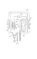
図1は、本発明の構成を適用し得るインクジェットヘッドを示す模式的な切断面部分図である。 FIG. 1 is a schematic sectional view showing an inkjet head to which the configuration of the present invention can be applied.
図1において、101はシリコン基板、102は熱酸化膜からなる蓄熱層を示すものであり、103は蓄熱を兼ねるSiO膜、SiN膜等からなる層間膜、104は発熱抵抗層、105はAl、Al−Si、Al−Cu等の金属材料からなる配線としての金属配線層、106はSiO膜、SiN膜等からなる絶縁層としても機能する保護層を示す。107は、保護層106の上に設けられ、発熱抵抗体の発熱に伴う化学的、物理的衝撃から電気熱変換素子を守るための上部保護層である。また、108は発熱抵抗層104の発熱抵抗体で発生した熱がインクに作用する熱作用部である。
In FIG. 1,
インクジェットヘッドにおける熱作用部は、発熱抵抗体での熱発生により高温にさらされると共に、インクの発泡、発泡後の泡収縮に伴い、キャビテーション衝撃やインクによる化学的作用を主に受ける部分である。そのため、熱作用部には、このキャビテーション衝撃やインクによる化学的作用から電気熱変換素子を保護するため、上部保護層107が設けられる。上部保護層107の上には、流路形成部材109を用いて、インクを吐出するための吐出口110を備えた吐出エレメントが形成される。
The thermal action part in the ink jet head is a part that is exposed to a high temperature due to heat generation by the heating resistor, and is mainly subjected to a cavitation impact and a chemical action by the ink as the ink foams and the foam shrinks after the foaming. Therefore, an upper
図2は、吐出エレメントの形成法を示す。 FIG. 2 shows a method for forming the discharge element.
図1のインクジェットヘッド用基体100と同じインクジェットヘッド用基体200の上に、最終的にインク液流路となる溶解可能な固体層201として、レジストをスピンコート法を用いて塗布する。該レジスト材は、ポリメチルイソプロペニルケトンからなり、ネガ型のレジストとして作用し、フォトリソグラフィ技術を用いてインク液流路の形状にパターニングする。続いて、液流路壁や吐出口を形成するために被覆樹脂層203を形成する。該被覆樹脂層203を形成する前に、密着性を向上させるためにシランカップリング処理等を適宜行うことができる。該被覆樹脂層203は、従来より知られているコーティング法を適宜選択することができ、インク液流路パターンが形成されたインクジェットヘッド用基体200に塗布することができる。その後、インクジェットヘッド用基体200の裏面から、異方性エッチング法、サンドブラスト法、異方性プラズマエッチング法等を用いて、インク液供給口206を形成する。最も好ましくは、テトラメチルヒドロキシアミン(TMAH)、NaOHやKOH等を用いた化学的シリコン異方性エッチング法により、インク液供給口206を形成することができる。続いて、溶解可能な固体層201を除去するために、Deep−UV光による全面露光を行い、現像、乾燥を行った。
On the same ink jet head substrate 200 as the ink
また図3に示すように、上部保護層107(Ta100−XCrX膜)形成後に、ノズル構成部材(流路形成部材109)との間に有機密着向上膜307を形成することもできる。有機密着向上膜307としては、ポリエーテルアミド樹脂を選択した。該樹脂はアルカリエッチング耐性に優れ、且つ、シリコン等の無機膜との密着性も良好であり、さらには、インクジェット記録ヘッドの耐インク保護膜としても用いることができる等の利点があり、特に好ましいものである。その後、フォトリソグラフィ技術により、例えば図3に示すような形状にパターニングを行う。このパターニングは、通常の有機膜のドライエッチングと同様の方法で行うことができる。すなわち、ポジ型のレジストをマスクとして、酸素ガスプラズマによりエッチングを行うことができる。
In addition, as shown in FIG. 3, after the formation of the upper protective layer 107 (Ta 100-X Cr X film), an organic
以下、上部保護層107(Ta100−XCrX膜)形成後に、有機密着向上膜307を形成する方法を図3にて説明する。インクジェット用基体300にスピンコート法にて、最終的にインク液流路となるべく溶解可能な固体層301として、レジストを塗布する。該レジスト材料は、ポリメチルイソプロペニルケトンから成り、ネガ型のレジストとして作用し、インク液流路の形状にフォトリソグラフィ技術によりパターニングされる。
Hereinafter, a method of forming the organic
続いて、液流路壁や吐出口を形成すべく被覆樹脂層303を形成する。該被覆樹脂層303を形成する前に、密着向上のためシランカップリング処理などを適宜行うことができる。被覆樹脂層303は、従来より知られているコーティング法を適宜選択することができ、インク液流路パターンが形成されたヒーター基板上に塗布することができる。塗布された被膜樹脂層303は、フォトリソグラフィ技術にてパターニングされる。その後、ヒーター基板裏面よりインク液供給口306として、異方性エッチング法、サンドブラスト法、異方性プラズマエッチングなどにより、ヒーター基板裏面からインク供給口を形成する。最も好ましくは、テトラメチルヒドロキシアミン(TMAH)、NaOHやKOH等を用いた化学的シリコン異方性エッチング法により、インク液供給口306を形成した。続いて、溶解可能な固体層301を除去すべく、Deep−UV光による全面露光を行った後、現像、乾燥を行った。
Subsequently, a
以上の図2、図3にて説明した工程によりノズル部が作成された基板を、ダイシングソーなどにより分離切断、チップ化し、発熱抵抗体を駆動するための電気的接合とインク供給部材の接合を行い、インクジェットヘッドが完成する。 2 and FIG. 3, the substrate on which the nozzle portion has been created is separated and cut into chips by a dicing saw or the like, and electrical bonding for driving the heating resistor and bonding of the ink supply member are performed. This completes the inkjet head.
このインクに接する上部保護層は、耐熱性、機械的特性、化学的安定性、耐酸化性、耐アルカリ性等に優れた膜特性が要求されると同時に、有機密着向上層や流路形成部材との密着性に優れていることが要求され、TaとCrからなる。好ましくはTa100−XCrXにおいてX≧12at.%から構成される。 Upper protective layer in contact with the ink, and heat resistance, mechanical properties, chemical stability, oxidation resistance, and at the same time excellent film properties in alkali resistance or the like is required, the organic adhesion improving layer and the flow path forming member It is required to be excellent in adhesion, and consists of Ta and Cr. Preferably, in Ta 100-X Cr X , X ≧ 12 at. %.
上部保護層107の膜厚は、50nm〜500nm、好ましくは100nm〜300nmから選択される。また、この上部保護層の膜応力は、少なくとも圧縮応力を有し、1.0×10 10 dyn/cm2以下であることが好ましい。なお、上部保護層107は、各種成膜法で作製可能であるが一般的には電源として高周波(RF)電源、または直流(DC)電源を用いたマグネトロンスパッタリング法により形成することができる。
The film thickness of the upper
図4は、上部保護層107を成膜するスパッタリング装置の概要を示すものである。図4において、4001はTaターゲットとCrターゲットの2種類からなる。4002は平板マグネット、4011は基板への成膜を制御するシャッター、4003は基板ホルダー、4004は基板、4006はターゲット4001と基板ホルダー4003に接続された電源である。さらに、図4において、4008は成膜室4009の外周壁を囲んで設けられた外部ヒーターである。外部ヒーター4008は、成膜室4009の雰囲気温度を調節するのに使用される。基板ホルダー4003の裏面には、基板の温度制御を行う内部ヒーター4005が設けられている。基板4004の温度制御は、外部ヒーター4008を併用して行うことが好ましい。
FIG. 4 shows an outline of a sputtering apparatus for forming the upper
図4の装置を用いた成膜は、次のように行われる。まず、排気ポンプ4007を用いて成膜室4009を1×10⁻⁵Pa〜1×10⁻⁶Paまで排気する。次いで、Arガスを、マスフローコントローラー(不図示)を介してガス導入口4010から成膜室4009に導入する。この時、基板温度及び雰囲気温度が所定の温度になるように内部ヒーター4005、外部ヒーター4008を調節する。次に、電源4006からターゲット4001にパワーを印加してスパッタリング放電を行い、シャッター4011を調節して、基板4004の上に薄膜を形成させる。
Film formation using the apparatus of FIG. 4 is performed as follows. First, the
本発明では、TaターゲットとCrターゲットの2種類からなり、それぞれに接続された2台の電源からパワーを印加する、2元同時スパッタリング法により形成することが可能である。この場合は、各々のターゲットに印加するパワーを単独に制御することが可能となる。あるいは、あらかじめ所望の組成に調整された合金ターゲットを複数用意し、それぞれを単独、あるいは複数のターゲットを同時にスパッタリングすることにより、所望の組成の薄膜を形成することができる。 In the present invention, the Ta target and the Cr target are used, and it can be formed by a binary simultaneous sputtering method in which power is applied from two power sources connected to each. In this case, the power applied to each target can be controlled independently. Alternatively, a thin film having a desired composition can be formed by preparing a plurality of alloy targets that have been adjusted in advance to a desired composition and sputtering each of them individually or simultaneously.
また、上述したように、上部保護層107の形成の際には、基板の温度を100℃〜300℃に加熱することにより強い膜密着力を得ることができる。また、上述したような比較的運動エネルギーの大きな粒子を形成できるスパッタリング法により成膜することにより、強い膜密着力を得ることができる。
Further, as described above, when the upper
更に、膜応力としては、少なくとも圧縮応力を有し、1.0×10¹⁰dyn/cm2以下にすることにより、同様に強い膜密着力を得ることができる。この膜応力は、成膜装置に導入するArガス流量やターゲットに印加するパワー、基板加熱温度を適宜設定することにより調整すればよい。 Furthermore, the film stress is at least a compressive stress, and by setting the film stress to 1.0 × 10 10 dyn / cm 2 or less, a strong film adhesion force can be obtained similarly. This film stress may be adjusted by appropriately setting the flow rate of Ar gas introduced into the film forming apparatus, the power applied to the target, and the substrate heating temperature.
また、図5は、本発明を適用し得るインクジェット装置の一例の外観図である。このインクジェット装置は旧式のタイプではあるが、本発明は最新のインクジェット装置に適用されることで、より一層効果を奏するものである。 FIG. 5 is an external view of an example of an ink jet apparatus to which the present invention can be applied. Although the ink jet apparatus is an old type, the present invention is more effective when applied to the latest ink jet apparatus.
図5のインクジェット装置において、記録ヘッド2200は、駆動モータ2101の正逆回転に連動して駆動力伝達ギア2102、2103を介して回転するリードスクリュー2104の螺旋溝2121に係合するキャリッジ2120上に搭載されており、駆動モータ2101の動力によってキャリッジ2120とともにガイド2119に沿って矢印a、b方向に往復移動される。不図示の記録媒体供給装置によってプラテン2106上に搬送される記録用紙P用の紙押え板2105は、キャリッジ2120移動方向にわたって記録用紙をプラテン2106に対して押圧する。
In the ink jet apparatus of FIG. 5, the
2107、2108はフォトカプラでキャリッジ2120のレバー2109のこの域での存在を確認して駆動モータ2101の回転方向切り替え等を行うためのホームポジション検知手段である。2110は記録ヘッド2200の全面をキャップするキャップ部材2111を支持する部材で、2112はキャップ部材2111内のインクを吸引排出するための吸引手段で、キャップ内開口2113を介して記録ヘッド2200の吸引回復を行う。2114はクリーニングブレードで、2115はこのブレードを前後方向に移動可能にする移動部材であり、本体支持板2116にこれらは支持されている。クリーニングブレード2114は、この形態でなく周知のクリーニングブレードが本体に適用できることは言うまでもない。
また、2117は、吸引回復の吸引を開始するためのレバーで、キャリッジ2120と係合するカム2118の移動に伴って移動し、駆動モータ2101からの駆動力がクラッチ切り替え等の公知の伝達手段で移動制御される。前記記録ヘッド2200に設けられて発熱部2110に信号を付与したり、上述した各機構の駆動制御を司ったりする記録制御部は、記録装置本体側に設けられている(不図示)。
上述したような構成のインクジェット記録装置2100は、記録媒体供給装置によってプラテン2106上に搬送される記録用紙Pに対し、記録ヘッド2200が記録用紙Pの全幅にわたって往復運動しながら記録を行うものであり、記録ヘッド2200は上述したような方法で製造したものを用いているため、高精度で高速な記録が可能である。
The ink
以下、上部保護層107の成膜例、およびそれらを用いたインクジェットヘッド等についての実施例により、本発明を更に詳細に説明する。なお、本発明は、かかる実施例等により限定されるものではない。
Hereinafter, the present invention will be described in more detail with reference to an example of forming the upper
図4に示した装置を使用し、かつ上述した成膜方法を利用して、上部保護層107用のTa−Cr薄膜をシリコンウエハ上に形成し、膜物性を評価した。その際の成膜操作及び膜物性の評価について以下に示す。
A Ta—Cr thin film for the upper
[成膜操作]
まず、単結晶シリコンウエハ上に熱酸化膜を形成し、このシリコンウエハ(基板4004)を図4の装置の成膜室4009内の基板ホルダー4003にセットした。次いで、排気ポンプ4007により成膜室4009内を8×10⁻⁶Paまで排気した。その後、Arガスをガス導入口4010から成膜室4009に導入し、成膜室40009内の条件を以下のようにした。
[Deposition operation]
First, a thermal oxide film was formed on a single crystal silicon wafer, and this silicon wafer (substrate 4004) was set on the
[成膜条件]
基板温度:200℃
成膜室内ガス雰囲気温度:200℃
成膜室内混合ガス圧力:0.6Pa
次いで、TaターゲットとCrターゲットを用いて、各ターゲットに投入するパワーを可変とした2元スパッタリング法により、シリコンウエハの熱酸化膜上に200nmの膜厚でTa100−XCrX膜を形成し、試料1〜7を得た。
[Film formation conditions]
Substrate temperature: 200 ° C
Gas atmosphere temperature in the deposition chamber: 200 ° C
Gas pressure in the deposition chamber: 0.6 Pa
Next, using a Ta target and a Cr target, a Ta 100-X Cr X film having a thickness of 200 nm is formed on the thermal oxide film of the silicon wafer by a binary sputtering method in which the power input to each target is variable. Samples 1 to 7 were obtained.
[膜物性評価]
得られた上記試料1〜7についてRBS(ラザフォード後方散乱)分析を行い、各試料の組成分析を行った。その結果を表1に示す。表1のように、TaとCrターゲットへの投入パワーを変えることにより、各種組成の膜を作製することが可能である。
[Evaluation of film properties]
The obtained samples 1 to 7 were subjected to RBS (Rutherford backscattering) analysis, and composition analysis of each sample was performed. The results are shown in Table 1. As shown in Table 1, it is possible to produce films having various compositions by changing the input power to the Ta and Cr targets.

[膜応力について]
次に、各試料の膜応力について、成膜の前後における基板変形量により測定した。その結果、Ta100−XCrX膜のCr濃度が増加するほど、膜応力は圧縮応力から引っ張り応力へと変化する傾向が見られ、膜の密着力の低下傾向が現れた。膜応力としては、少なくとも圧縮応力を示し、1.0×10¹⁰dyn/cm2以下にすることにより、同様に強い膜密着力を得ることができる。
[About film stress]
Next, the film stress of each sample was measured by the amount of substrate deformation before and after film formation. As a result, as the Cr concentration of the Ta 100-X Cr X film increased, the film stress tended to change from a compressive stress to a tensile stress, and a tendency to decrease the adhesion of the film appeared. As the film stress, at least compressive stress is shown, and by setting the film stress to 1.0 × 10 10 dyn / cm 2 or less, a strong film adhesion force can be obtained similarly.
[樹脂との密着性について]
(実施例1)
本実施例のTa88Cr12膜107(組成比がTa88at%、Cr12at%の膜を表す。以下、同様。)と有機密着向上膜(ポリエーテルアミド樹脂)307との密着性を簡易的に評価するために、テープ引き剥がし試験をPCT(Pressure Cooker Test)後に行った。
[Adhesion with resin]
Example 1
The adhesion between the Ta 88 Cr 12 film 107 (composition ratio of Ta 88 at % and Cr 12 at %; the same applies hereinafter) of this example and the organic adhesion improving film (polyether amide resin) 307 is simply evaluated. In order to achieve this, a tape peeling test was performed after PCT (Pressure Cooker Test).
テープ引き剥がし試験は次のように行った。上部保護層107が形成されたシリコンウエハ上に、有機密着向上膜(ポリエーテルアミド樹脂)307を膜厚2μmに形成し、カッターナイフを用いて1mm×1mm角の碁盤目状のマス目を10×10=100(縦×横)個、有機密着向上膜307上に形成した。続いて、121℃、2.0265×10⁵Pa(2atom)で10hr、アルカリインク中に浸漬する条件でPCT試験を行った。その後に、上記碁盤目状のマス目の部分にテープを貼り、テープによる引き剥がしを行い、100個の中でテープにより引き剥がされた数を調べた。その結果、100個中15個程度の剥がれが発生したが、全体的には良好な結果であった。(表2)
The tape peeling test was performed as follows. An organic adhesion improving film (polyether amide resin) 307 is formed to a thickness of 2 μm on the silicon wafer on which the upper
(比較例1)
実施例1と同様の方法を用いて、Ta膜と有機密着向上膜(ポリエーテルアミド樹脂)307との密着性について、PCT後の密着性の評価を行い、その結果を表2に示す。
(Comparative Example 1)
Using the same method as in Example 1, the adhesion between the Ta film and the organic adhesion improving film (polyetheramide resin) 307 was evaluated for adhesion after PCT, and the results are shown in Table 2.
表2のように、PCT試験後にはTa膜と有機密着向上膜307との界面から剥がれが発生し、密着性の低下が顕著であった。
As shown in Table 2, peeling occurred from the interface between the Ta film and the organic
(実施例2〜7)
実施例1と同様の方法を用いて、組成の異なるTa100−XCrX膜について、PCT後の密着性の評価を行い、その結果を表2に示す。
(Examples 2 to 7)
Using the same method as in Example 1, the Ta 100-X Cr X films having different compositions were evaluated for adhesion after PCT, and the results are shown in Table 2.
(比較例2〜3)
実施例1と同様の方法を用いて、PCT後の密着性の評価を行った。比較例としてTa20Fe61Cr14Ni5(比較例2)、Ta87Fe10Cr2Ni1(比較例3)について評価を行った。これらの結果を表2に示す。
(Comparative Examples 2-3)
Using the same method as in Example 1, the adhesion after PCT was evaluated. As comparative examples, Ta 20 Fe 61 Cr 14 Ni 5 (Comparative Example 2) and Ta 87 Fe 10 Cr 2 Ni 1 (Comparative Example 3) were evaluated. These results are shown in Table 2.
これらの比較例で明らかなように、従来上部保護層として用いられているTa20Fe61Cr14Ni5、Ta87Fe10Cr2Ni1膜においては、上部保護層107と有機密着向上膜307との界面から剥がれが生じ、十分な密着性を得ることができなかった。
As is clear from these comparative examples, in the Ta 20 Fe 61 Cr 14 Ni 5 and Ta 87 Fe 10 Cr 2 Ni 1 films conventionally used as the upper protective layer, the upper
以上のように、PCT試験を行った後の上部保護層107と有機密着向上膜307との密着性は、Ta100−XCrX膜においては、Cr組成が少ない膜で低下する傾向があり、Xが12at.%以上では良好な結果であった。
As described above, the adhesion between the upper
以上は、密着向上層がある場合の結果を示したが、密着向上層がない場合も同様の傾向を示し、密着向上層の有無にかかわらずTa100−XCrX膜(X≧12at.%)は密着性に対して効果のあることがわかった。 The above shows the results when there is an adhesion improving layer, but the same tendency is shown when there is no adhesion improving layer, and a Ta 100-X Cr X film (X ≧ 12 at.%) Regardless of the presence or absence of the adhesion improving layer. ) Was found to be effective for adhesion.
[インクジェット用特性評価]
(実施例8)
本実施例によるインクジェット特性としての評価を行う試料の基板は、Si基板あるいはすでに駆動用のICを作り込んだSi基板を用いる。Si基板の場合は、熱酸化法、スパッタ法、CVD法などによって膜厚1.8μmのSiO2の蓄熱層102(図1)を形成し、ICを作り込んだSi基板も同様にその製造プロセス中で、SiO2の蓄熱層を形成しておく。
[Characteristic evaluation for inkjet]
(Example 8)
As a sample substrate to be evaluated as ink jet characteristics according to this embodiment, a Si substrate or a Si substrate in which a driving IC has already been formed is used. In the case of a Si substrate, a SiO 2 heat storage layer 102 (FIG. 1) having a film thickness of 1.8 μm is formed by thermal oxidation, sputtering, CVD, etc., and the manufacturing process of the Si substrate in which an IC is formed is also the same. Inside, a heat storage layer of SiO 2 is formed.
次に、スパッタ法、CVD法などによってSiO2からなる膜厚1.2μmの層間絶縁膜103を形成した。次いで、Ta−Siターゲットを用いた反応性スパッタリング法により、50nmのTa40Si21N39発熱抵抗体層104を形成した。この時の基板温度は200℃で行った。金属配線105としてAl膜を200nmの膜厚にスパッタリング法により形成した。
Next, an
次に、フォトリソグラフィ法を用いてパターン形成し、Al膜を取り除いた26μm×26μmの熱作用部108を形成した。次に、保護膜106としてプラズマCVD法によってSiNからなる膜厚300nmの絶縁体を形成した。
Next, a pattern was formed using a photolithography method to form a 26 μm × 26 μm
次に、上部保護層107として、TaターゲットとCrターゲットに印加するパワーを変えながら、スパッタリング法により、Ta88Cr12膜を200nm形成した。
Next, as the upper
次に、上部保護層107をドライエッチングにより、パターニングを行った。
Next, the upper
続いて、上部保護層と流路形成部材との密着性を向上させるために、有機密着向上膜(ポリエーテルアミド樹脂)307を膜厚2μmに形成し、インクジェットヘッド用基体を作製した。 Subsequently, in order to improve the adhesion between the upper protective layer and the flow path forming member , an organic adhesion improving film (polyether amide resin) 307 was formed to a thickness of 2 μm to produce an inkjet head substrate.
これらのインクジェット用基体を用いて図3で示した製造方法によりインクジェットヘッドを作製し、更にインクジェット記録装置を用いて、吐出耐久試験を行った。この試験は、駆動周波数15KHz、パルス幅は1.0μsec.とし、2.0×10⁸パルス時点での上部保護層107のケズレの様子を、FIBを用いた断面観察により評価した。この時の駆動電圧は、1.3×Vthとした。尚、Vthはインクを吐出する発泡閾値電圧を示す。また、インクは、硝酸基の入った二価金属塩Ca(NO3)2・4H2Oを4%程度含有するインクを用いた。
Using these ink jet bases, an ink jet head was produced by the production method shown in FIG. 3, and a discharge durability test was conducted using an ink jet recording apparatus. In this test, the driving frequency was 15 KHz and the pulse width was 1.0 μsec. 2 . The state of scratching of the upper
表3のように、2.0×10⁸パルス数まで連続吐出を行っても僅かなケズレが発生しているが、吐出特性は安定しており上部保護層として安定であることがわかった。 As shown in Table 3, it was found that even if continuous ejection was performed up to the number of 2.0 × 10 8 pulses, slight damage occurred, but the ejection characteristics were stable and the upper protective layer was stable.
(比較例4)
上部保護層107をTa膜で形成する以外は実施例8と同様にしてインクジェット用ヘッドを作製した。このインクジェット用ヘッドを用いて実施例1と同様にして吐出耐久試験を行い、その結果を表3に示す。表3のように、比較例1では2×10⁸パルス以前に吐出することができなくなった。そこで、インクジェット用ヘッドを分解して解析を行った結果、その腐食が発熱抵抗層まで達し、発熱抵抗層が断線していることが判明した。
(Comparative Example 4)
An inkjet head was manufactured in the same manner as in Example 8 except that the upper
(実施例9〜16)
上部保護層107を表3に示すような組成、膜厚で形成する以外は実施例8と同様にしてインクジェット用ヘッドを作製した。このインクジェット用ヘッドを用いて実施例8と同様にして吐出耐久試験を行い、その結果を表3に示す。
(Examples 9 to 16)
An inkjet head was produced in the same manner as in Example 8 except that the upper
(比較例5〜6)
上部保護層107を表3に示すような組成、膜厚で形成する以外は実施例8と同様にしてインクジェット用ヘッドを作製した。
(Comparative Examples 5-6)
An inkjet head was produced in the same manner as in Example 8 except that the upper
このインクジェット用ヘッドを用いて実施例8と同様にして吐出耐久試験を行い、その結果を表3に示す。 Using this inkjet head, a discharge durability test was conducted in the same manner as in Example 8, and the results are shown in Table 3.
表3のように、Ta20Fe61Cr14Ni5(比較例5)においては、殆どケズレが発生しておらず、吐出耐久に対して安定であることがわかった。 As shown in Table 3, it was found that in Ta 20 Fe 61 Cr 14 Ni 5 (Comparative Example 5 ), almost no scratches were generated and the discharge durability was stable.
Ta87Fe10Cr2Ni1(比較例6)においては、膜厚の半分程度までケズレが発生していることがわかった。 In Ta 87 Fe 10 Cr 2 Ni 1 (Comparative Example 6 ), it was found that scratches occurred up to about half of the film thickness.
以上の結果から、次のことが明らかになった。 From the above results, the following became clear.
すなわち、表3の結果から明らかなように、吐出耐久における上部保護層107のケズレに対する安定性は、Ta100−XCrX膜の組成に依存し、特にCr組成が多いほど優れていることが解った。つまり、上部保護層107のTa100−XCrXの組成はX≧12at.%であるとケズレに対して極めて安定であることが明らかとなった。
That is, as is apparent from the results in Table 3, the stability of the upper
また、上部保護層107の膜厚は、100nm以上500nm以下であることが好ましい。膜厚が100nm未満であると、インクに対する保護機能が十分でなく、500nmより厚いと発熱抵抗体層からのエネルギーがインクに有効に伝達されず、エネルギー損失が大きくなる場合がある。
The thickness of the upper
上記各実施例では、膜厚が100nm程度でも優れた耐久性を得ることが可能であった。また、膜応力としては、少なくとも圧縮応力を有し、1.0×10¹⁰dyn/cm2以下にすることにより強い膜付着力を得ることができ、同様に優れた耐久性を得ることが可能であった。 In each of the above examples, excellent durability could be obtained even when the film thickness was about 100 nm. Moreover, as a film stress, it has at least a compressive stress, and by setting it to 1.0 × 10 10 dyn / cm 2 or less, a strong film adhesion can be obtained, and similarly excellent durability can be obtained. Met.
以上、説明したような各実施例によれば、上部保護層107が、TaとCrの合金からなり、上部保護層107の上部に樹脂(流路形成部材109)が形成されているとともに、該樹脂が上部保護層107に固定されることにより、高密度化を可能とインクジェットヘッド用基体、該基体を備えたインクジェットヘッド、及び該インクジェットヘッドを備えたインクジェット装置を提供することが可能となった。
According to each embodiment as described above, the upper
(実施例17)
ここで説明する実施例は、上部保護層107が2層構成となっており、熱作用部ではTaよりなる上層111、TaCrよりなる下層112の2層構成、流路形成部材109の下部では下層112のみの1層構成となっている。
(Example 17)
In the embodiment described here, the upper
具体的には、上部保護層107の下層膜112としてTa80Cr20膜、上層膜111としてTa膜を用いた場合を示す。
Specifically, a case where a Ta 80 Cr 20 film is used as the
下層112は、TaターゲットとCrターゲットを用いた2元スパッタリング法により成膜し、Ta80Cr20組成で130nm絶縁層上に形成した。尚、2元スパッタリングの条件はTaスパッタリングパワーとCrスパッタリングパワーを各々可変させて、予め組成分析を行うことにより条件設定を行った。また、2元スパッタリング法でなくとも、予め組成比のわかっているTaCr合金ターゲットを用いたスパッタリングで行っても良い。
The
その後、Taターゲットを用いて、スパッタリング法により上層111を100nm形成した。この際、同一スパッタリングチャンバーで、連続的に膜形成を行った。 Thereafter, an upper layer 111 was formed to a thickness of 100 nm by sputtering using a Ta target. At this time, the film was continuously formed in the same sputtering chamber.
その後、まず上層111のTa膜のパターン形成を、一般的なフォトリソグラフィプロセスを用い、レジストパターニング(レジスト塗布、露光、現像)、Taエッチング、レジスト剥離の順に行った。 After that, first, pattern formation of the Ta film of the upper layer 111 was performed in the order of resist patterning (resist application, exposure, development), Ta etching, and resist peeling using a general photolithography process.
この際、Ta膜のパターン形状は、露光時のフォトマスクパターンにより所望のパターンを選択することができる。そこで、図6と図7に示すように発熱部(熱作用部108)上にTa膜のパターンを形成し、流路形成部材109が形成される箇所には上層111であるTa膜を形成しないようにした。次に、TaCr膜のパターン形成を、フォトリソグラフィプロセスを用い、レジストパターニング(レジスト塗布、露光、現像)、TaCr膜のエッチング、レジスト剥離の順に行った。
At this time, as the pattern shape of the Ta film, a desired pattern can be selected according to the photomask pattern at the time of exposure. Therefore, as shown in FIGS. 6 and 7, a Ta film pattern is formed on the heat generating part (thermal action part 108), and the Ta film which is the upper layer 111 is not formed at the place where the flow
ここで、図6において、1090は一部領域に有機密着向上層307の上に流路形成部材109を積層した構成を含む流路部材形成部、1110は上部保護層上層部パターン、1120は上部保護層下層部パターン、1080は発熱抵抗体、1050は電極配線部である。
Here, in FIG. 6,
なお、TaCr膜のエッチングはドライエッチング装置を用い、下地の絶縁保護層とのエッチング選択比がとれるエッチングガス種、ガス圧力、パワーを選択した。TaCr膜のパターン形状を形成する際には、図6に示すように、流路部材形成部1090の下部に、TaCr膜のパターンが形成されるようにした。
Etching of the TaCr film was performed using a dry etching apparatus, and an etching gas type, gas pressure, and power capable of obtaining an etching selectivity with the underlying insulating protective layer were selected. When forming the pattern shape of the TaCr film, as shown in FIG. 6, the pattern of the TaCr film is formed below the flow path
また、図7にその断面構成を示すように、上部保護層107の下層膜112としての膜厚230nmのTa80Cr20膜の上には、下部流路形成部材となる有機密着向上膜307と流路形成部材109とをこの順に積層したものを用い、Ta80Cr20膜と、その上の下部流路形成部材の有機密着向上膜307及び流路形成部材109と、の密着性を簡易的に評価した。試験は、テープ引き剥がし試験を、初期状態とPCT(Pressure Cooker Test)後に行った。この下部流路形成部材としての有機密着向上膜307は、流路形成部材109とTaCr膜との密着性を更に強固にすることを目的とするため、今回用いたものである。
Also, as shown the cross-sectional configuration in FIG. 7, on the Ta80Cr20 film having a thickness of 230nm as a
PCTは、密着向上層307上に流路形成部材を形成したものを、121℃、2.0265×10⁵Pa(2atm)、10hrの条件でアルカリインク中に浸漬する条件で行った。この結果を表4に示す。この結果より、Ta80Cr20膜の密着性は問題ないことがわかった。
PCT was performed under the condition that a flow path forming member formed on the
上部保護層107の下層112であるTa80Cr20膜及び上層111であるTa膜のパターン形成後、該基板上に溶解可能な固体層301をスピンコート法により塗布し、露光することにより、インク流路となるべき形状を作成した。インク流路の形状は、通常のマスクとDeep−UV光を用いて得ることができた。その後、被覆樹脂層303を積層し、露光装置を用いて露光後、現像することで吐出口110を形成した。続いて、TMAHにて、化学的シリコン異方性エッチング法により、インク供給口306を形成した後、Deep−UV光を全面照射し、現像、乾燥することにより、被覆樹脂層303の溶解すべき部位を除去した。以上の工程により、ノズル部が形成された基板をダイシングソーなどにより分離切断、チップ化し、発熱抵抗体を駆動するための電気的接合とインク供給部材の接合を行い、インクジェットヘッドを完成させた。
After forming a pattern of the Ta 80 Cr 20 film as the
ここで作製したインクジェットヘッドを用いてpH10のアルカリインクを吐出評価したところ、良好な記録品のものを得ることができた。また、このインク中にインクジェットヘッドを、60℃、3ヶ月浸漬させた後、吐出記録評価を行ったところ、良好な記録品位のものを得ることができたとともに、被覆樹脂層303の剥離は確認されなかった。
When an alkaline ink having a pH of 10 was discharged and evaluated using the ink jet head produced here, a good recording product could be obtained. In addition, after the ink jet head was immersed in this ink at 60 ° C. for 3 months and then evaluated for ejection recording, a good recording quality was obtained and peeling of the
(比較例7)
上部保護層としてTaのみの単層膜を用いた場合を示す。
(Comparative Example 7)
The case where a single-layer film made only of Ta is used as the upper protective layer is shown.
本比較例では、Taターゲットを用いて、スパッタリング法により膜厚230nmのTa膜を形成した。 In this comparative example, a Ta film having a thickness of 230 nm was formed by sputtering using a Ta target.
その後、Ta膜のパターン形成を、一般的なフォトリソプロセスを用い、レジストパターニング(レジスト塗布、露光、現像)、Taエッチング、レジスト剥離の順に行った。 Thereafter, patterning of the Ta film was performed in the order of resist patterning (resist application, exposure, development), Ta etching, and resist stripping using a general photolithography process.
この際、Ta膜のパターン形状は露光時のフォトマスクパターンにより所望のパターンを選択することができる。 At this time, a desired pattern can be selected as the pattern shape of the Ta film according to the photomask pattern at the time of exposure.
また、膜厚230nmのTa膜と、流路形成部材109及び下部流路形成部材となる有機密着向上膜307と、の密着性を簡易的に評価するため、テープ引き剥がし試験を行った。試験は、テープ引き剥がし試験を、初期状態とPCT後に行った。
Further, in order to easily evaluate the adhesion between the Ta film having a thickness of 230 nm and the organic
PCTは、密着向上層307上に流路形成部材109を形成したものを、121℃、2.0265×10⁵Pa(2atm)、10hrの条件でアルカリインク中に浸漬する条件で行った。この結果を表4に示す。
The PCT was performed under the condition that the
この結果より,Ta膜はPCT後に剥れが見られたことから、密着性に関しては、上記実施例17で挙げた、上部保護層107の下層膜112としてのTa80Cr20を、上層膜111としてのTa膜を用いたもののほうが優れていることが確認された。
From this result, since the Ta film was peeled after PCT, regarding the adhesiveness, Ta 80 Cr 20 as the
その後、上部保護層107を形成した基板上に溶解可能な固体層301をスピンコート法により塗布し、露光することにより、インク流路となるべき形状を作成した。インク流路の形状は、通常のマスクとDeep−UV光を用いて得ることができた。その後、被覆樹脂層303を積層し、露光装置を用いて露光後、現像することで吐出口110を形成した。続いて、TMAHにて、化学的シリコン異方性エッチング法により、インク供給口306を形成した後、Deep−UV光を全面照射し、現像、乾燥することにより、被覆樹脂層303の溶解すべき部位を除去した。以上の工程により、ノズル部が形成された基板をダイシングソーなどにより分離切断、チップ化し、発熱抵抗体を駆動するための電気的接合とインク供給部材の接合を行い、インクジェットヘッドを完成させた。
After that, a soluble
そして、このインクジェットヘッドを用いてpH10のアルカリインクを吐出評価したところ、良好な記録品位のものを得ることができた。しかしながら、このインクにインクジェットヘッドを、60℃、3ヶ月浸漬させた後、吐出記録評価を行ったところ、不吐出の部分が観察され、良好な記録品位のものを得ることはできなかった。インクジェットヘッドを観察したところ、被覆樹脂層303の剥離が観察され各々インク流路の連結が確認された。
When this ink jet head was used to evaluate the discharge of alkaline ink having a pH of 10, it was possible to obtain a good recording quality. However, when the ink jet head was immersed in this ink at 60 ° C. for 3 months and then was evaluated for ejection recording, a non-ejection portion was observed, and it was not possible to obtain a recording quality of good quality. When the ink jet head was observed, peeling of the
この実施例によれば、ヒーター基板上の上部保護膜の液流路部材と接する下層にTaCr膜を、発熱部上でインクと接する上層にTa膜を形成することにより、記録画像の高精細化に対応した小ドット化や高速記録に対応した長尺化、あるいは多様なインクを用いた場合にも上部保護層と液流路を形成する樹脂層との密着性が改善され、高密度化を可能とするインクジェットヘッド用基体、インクジェットヘッド及び該インクジェットヘッドを備えたインクジェットヘッド装置を提供することが可能となった。 According to this embodiment, by forming a TaCr film on the lower layer in contact with the liquid flow path member of the upper protective film on the heater substrate and forming a Ta film on the upper layer in contact with the ink on the heat generating portion, high-definition of the recorded image is achieved. In addition, the adhesion between the upper protective layer and the resin layer that forms the liquid flow path is improved even when various dots are used. An ink jet head substrate, an ink jet head, and an ink jet head device including the ink jet head can be provided.
さらに、上部保護層を2層化することにより、コゲーションによる吐出不安定性の高いインク、腐食性の高いインク等の多様なインクに対しても、耐久性、高信頼性が得られ、高寿命のインクジェットヘッド用基体、インクジェットヘッド及び該インクジェットヘッドを備えたインクジェット装置の提供が可能となった。 Furthermore, by forming the upper protective layer into two layers, durability and high reliability can be obtained for various inks such as ink with high ejection instability due to kogation and highly corrosive ink, and has a long service life. It is possible to provide an inkjet head substrate, an inkjet head, and an inkjet apparatus including the inkjet head.
尚、上述の各実施例は、フォトリソグラフィ技術を用いて吐出口、インク流路等の吐出エレメント部を形成したインクジェット記録ヘッドについて説明してきたが、吐出口となるオリフィスプレートやインク流路を形成する天板を別体で接着剤等により上部保護層の上に形成したものも包含するものである。 In each of the above-described embodiments, the ink jet recording head in which the discharge element portion such as the discharge port and the ink flow path is formed by using the photolithography technique has been described. However, the orifice plate or the ink flow path that becomes the discharge port is formed. It also includes a separate top plate formed on the upper protective layer by an adhesive or the like.
100 インクジェットヘッド用基体
101 シリコン基板
102 蓄熱層
103 層間膜
104 発熱抵抗層
105 金属配線
106 保護層
107 上部保護層
108 熱作用部
109 流路形成部材
110 吐出口
DESCRIPTION OF
Claims (6)
インクを吐出するためのエネルギーを発生するための発熱抵抗体が形成された基板と、
前記発熱抵抗体に電気的に接続する電極配線と、
前記発熱抵抗体と前記電極配線との上方に設けられ、膜応力が1.0×10 10 dyn/cm 2 以下の圧縮応力であり、膜厚が100nm以上500nm以下である、14at.%以上73at.%以下のCrを含有するTaCr合金からなる上部保護層と、
を有し、前記上部保護層は、その上部に樹脂製の構成物が形成され、該樹脂製の構成物は、有機密着向上層を介して当該上部保護層に固定されていることを特徴とするインクジェットヘッド用基体。 In an inkjet head substrate used for an inkjet head,
A substrate on which a heating resistor for generating energy for discharging ink is formed;
An electrode wiring electrically connected to the heating resistor;
14 at. 14 which is provided above the heating resistor and the electrode wiring , has a film stress of 1.0 × 10 10 dyn / cm 2 or less, and a film thickness of 100 nm to 500 nm. % Or more and 73 at. An upper protective layer made of a TaCr alloy containing not more than% Cr,
The upper protective layer is characterized in that a resin component is formed on the upper protective layer, and the resin component is fixed to the upper protective layer via an organic adhesion improving layer. An inkjet head substrate.
前記1層構成の部分は、前記下層が有機密着向上層を介して樹脂製の構成物としての流路形成部材を固定しているとともに、
前記2層構成の部分の前記上層は、少なくとも発熱抵抗体の上方のインクと接する位置に設けられていることを特徴とする請求項1に記載のインクジェットヘッド用基体。 The upper protective layer has a two-layer part composed of a TaCr alloy in the lower layer and Ta as the upper layer and a one-layer part only of the lower layer,
In the part of the one-layer configuration, the lower layer fixes a flow path forming member as a resin component via an organic adhesion improving layer,
2. The inkjet head substrate according to claim 1, wherein the upper layer of the two-layer structure is provided at a position in contact with at least the ink above the heating resistor.
前記インク吐出口に連通し、インクを吐出するための熱エネルギーをインクに作用させる部分を有するインク流路と、
請求項1乃至3のいずれか1項に記載のインクジェットヘッド用基体と、
を有することを特徴とするインクジェットヘッド。 In an inkjet head that ejects ink from an ink ejection port,
An ink flow path having a portion that communicates with the ink discharge port and causes thermal energy to discharge the ink to act on the ink;
An ink jet head substrate according to any one of claims 1 to 3 ,
An ink jet head comprising:
膜応力が1.0×10 10 dyn/cm 2 以下の圧縮応力であり、膜厚が100nm以上500nm以下である、14at.%以上73at.%以下のCrを含有するTaCr合金で形成した層の上に、Ta層を積層して前記上部保護層を形成した後、前記Ta層を選択的にパターニングして当該Ta層を選択的に除去することで、前記TaCr合金で形成された層が露出した部分に有機密着向上層を介して前記流路形成部材を形成することを特徴とするインクジェットヘッドの製造方法。 A heating resistor that forms a heating portion on the substrate, an electrode wiring that is electrically connected to the heating resistor, and a contact surface that contacts the ink and is provided above the heating resistor and the electrode wiring. In the method of manufacturing an inkjet head having an upper protective layer and a flow path forming member as a resin structure,
The film stress is a compressive stress of 1.0 × 10 10 dyn / cm 2 or less, and the film thickness is 100 nm or more and 500 nm or less, 14 at. % Or more and 73 at. % On the layer formed by TaCr alloy containing less Cr, after forming the upper protective layer by stacking a Ta layer, selectively removing the Ta layer by selectively patterning the Ta layer Then, the flow path forming member is formed through the organic adhesion improving layer in a portion where the layer formed of the TaCr alloy is exposed.
Priority Applications (5)
| Application Number | Priority Date | Filing Date | Title |
|---|---|---|---|
| JP2003413498A JP4078295B2 (en) | 2002-12-27 | 2003-12-11 | Ink-jet head substrate, ink-jet head using the same, and method for producing the same |
| PCT/JP2003/016712 WO2004060681A1 (en) | 2002-12-27 | 2003-12-25 | Substrate for ink jet head, ink jet head utilizing the same and producing method therefor |
| AU2003295234A AU2003295234A1 (en) | 2002-12-27 | 2003-12-25 | Substrate for ink jet head, ink jet head utilizing the same and producing method therefor |
| US10/534,906 US7393084B2 (en) | 2002-12-27 | 2003-12-25 | Substrate for ink jet head with TaCr alloy protective layer, ink jet head utilizing the same and producing method therefor |
| TW092137120A TW200413176A (en) | 2002-12-27 | 2003-12-26 | Substrate for ink jet head, ink jet head utilizing the same and producing method therefor |
Applications Claiming Priority (3)
| Application Number | Priority Date | Filing Date | Title |
|---|---|---|---|
| JP2002380823 | 2002-12-27 | ||
| JP2002380822 | 2002-12-27 | ||
| JP2003413498A JP4078295B2 (en) | 2002-12-27 | 2003-12-11 | Ink-jet head substrate, ink-jet head using the same, and method for producing the same |
Publications (3)
| Publication Number | Publication Date |
|---|---|
| JP2004216875A JP2004216875A (en) | 2004-08-05 |
| JP2004216875A5 JP2004216875A5 (en) | 2007-01-25 |
| JP4078295B2 true JP4078295B2 (en) | 2008-04-23 |
Family
ID=32718771
Family Applications (1)
| Application Number | Title | Priority Date | Filing Date |
|---|---|---|---|
| JP2003413498A Expired - Fee Related JP4078295B2 (en) | 2002-12-27 | 2003-12-11 | Ink-jet head substrate, ink-jet head using the same, and method for producing the same |
Country Status (5)
| Country | Link |
|---|---|
| US (1) | US7393084B2 (en) |
| JP (1) | JP4078295B2 (en) |
| AU (1) | AU2003295234A1 (en) |
| TW (1) | TW200413176A (en) |
| WO (1) | WO2004060681A1 (en) |
Cited By (1)
| Publication number | Priority date | Publication date | Assignee | Title |
|---|---|---|---|---|
| US11433674B2 (en) * | 2020-01-22 | 2022-09-06 | Canon Kabushiki Kaisha | Liquid discharge head and method for producing liquid discharge head |
Families Citing this family (9)
| Publication number | Priority date | Publication date | Assignee | Title |
|---|---|---|---|---|
| JP4208794B2 (en) * | 2004-08-16 | 2009-01-14 | キヤノン株式会社 | Inkjet head substrate, method for producing the substrate, and inkjet head using the substrate |
| JP4646602B2 (en) * | 2004-11-09 | 2011-03-09 | キヤノン株式会社 | Manufacturing method of substrate for ink jet recording head |
| JP4241605B2 (en) * | 2004-12-21 | 2009-03-18 | ソニー株式会社 | Method for manufacturing liquid discharge head |
| JP2006327180A (en) * | 2005-04-28 | 2006-12-07 | Canon Inc | Substrate for inkjet recording head, inkjet recording head, inkjet recording device and method for manufacturing substrate for inkjet recording head |
| JP4926669B2 (en) * | 2005-12-09 | 2012-05-09 | キヤノン株式会社 | Inkjet head cleaning method, inkjet head, and inkjet recording apparatus |
| US7824560B2 (en) * | 2006-03-07 | 2010-11-02 | Canon Kabushiki Kaisha | Manufacturing method for ink jet recording head chip, and manufacturing method for ink jet recording head |
| JP4854336B2 (en) * | 2006-03-07 | 2012-01-18 | キヤノン株式会社 | Manufacturing method of substrate for inkjet head |
| JP5311975B2 (en) * | 2007-12-12 | 2013-10-09 | キヤノン株式会社 | Substrate for liquid ejection head and liquid ejection head using the same |
| KR20090062012A (en) * | 2007-12-12 | 2009-06-17 | 삼성전자주식회사 | Inkjet head and method for manufacturing the same |
Family Cites Families (8)
| Publication number | Priority date | Publication date | Assignee | Title |
|---|---|---|---|---|
| JPH0613219B2 (en) * | 1983-04-30 | 1994-02-23 | キヤノン株式会社 | Inkjet head |
| JP3143307B2 (en) | 1993-02-03 | 2001-03-07 | キヤノン株式会社 | Method of manufacturing ink jet recording head |
| JP3647365B2 (en) | 1999-08-24 | 2005-05-11 | キヤノン株式会社 | Substrate unit for liquid discharge head, method for manufacturing the same, liquid discharge head, cartridge, and image forming apparatus |
| JP3576888B2 (en) | 1999-10-04 | 2004-10-13 | キヤノン株式会社 | Substrate for inkjet head, inkjet head, and inkjet apparatus |
| JP2001171126A (en) | 1999-10-05 | 2001-06-26 | Canon Inc | Substrate for ink-jet head with heating resistance element, ink-jet head using the same, ink-jet apparatus and recording method |
| JP3720689B2 (en) | 2000-07-31 | 2005-11-30 | キヤノン株式会社 | Inkjet head substrate, inkjet head, inkjet head manufacturing method, inkjet head usage method, and inkjet recording apparatus |
| JP4208793B2 (en) | 2004-08-16 | 2009-01-14 | キヤノン株式会社 | Inkjet head substrate, method for producing the substrate, and inkjet head using the substrate |
| JP4208794B2 (en) | 2004-08-16 | 2009-01-14 | キヤノン株式会社 | Inkjet head substrate, method for producing the substrate, and inkjet head using the substrate |
-
2003
- 2003-12-11 JP JP2003413498A patent/JP4078295B2/en not_active Expired - Fee Related
- 2003-12-25 AU AU2003295234A patent/AU2003295234A1/en not_active Abandoned
- 2003-12-25 US US10/534,906 patent/US7393084B2/en not_active Expired - Fee Related
- 2003-12-25 WO PCT/JP2003/016712 patent/WO2004060681A1/en active Application Filing
- 2003-12-26 TW TW092137120A patent/TW200413176A/en unknown
Cited By (1)
| Publication number | Priority date | Publication date | Assignee | Title |
|---|---|---|---|---|
| US11433674B2 (en) * | 2020-01-22 | 2022-09-06 | Canon Kabushiki Kaisha | Liquid discharge head and method for producing liquid discharge head |
Also Published As
| Publication number | Publication date |
|---|---|
| US20060061626A1 (en) | 2006-03-23 |
| AU2003295234A1 (en) | 2004-07-29 |
| TW200413176A (en) | 2004-08-01 |
| JP2004216875A (en) | 2004-08-05 |
| WO2004060681A1 (en) | 2004-07-22 |
| US7393084B2 (en) | 2008-07-01 |
Similar Documents
| Publication | Publication Date | Title |
|---|---|---|
| JP5393275B2 (en) | Liquid discharge head | |
| JP3576888B2 (en) | Substrate for inkjet head, inkjet head, and inkjet apparatus | |
| JP4078295B2 (en) | Ink-jet head substrate, ink-jet head using the same, and method for producing the same | |
| JP3962719B2 (en) | Ink-jet head substrate, ink-jet head using the same, and method for producing the same | |
| JP5311975B2 (en) | Substrate for liquid ejection head and liquid ejection head using the same | |
| JP4646602B2 (en) | Manufacturing method of substrate for ink jet recording head | |
| JP3402618B2 (en) | Method and apparatus for manufacturing ink jet recording head | |
| JP5679688B2 (en) | Liquid discharge head and manufacturing method thereof | |
| JP3710364B2 (en) | Inkjet head | |
| JP2007230127A (en) | Manufacturing method of substrate for inkjet recording head | |
| JP3554148B2 (en) | Substrate for inkjet recording head, inkjet recording head, and inkjet recording apparatus | |
| CN100493912C (en) | Substrate for ink jet head, ink jet head utilizing the same and producing method therefor | |
| JPH07125218A (en) | Heating resistor, substrate for liquid jetting head equipped with heating resistor, liquid jetting head equipped with substrate and liquid jetting apparatus equipped with liquid jetting head | |
| CN100496979C (en) | Substrate for ink jet head, ink jet head using the same, and manufacturing method thereof | |
| JPH10114072A (en) | Substrate for ink-jet recording head, manufacture thereof, ink-jet recording head having the substrate, and manufacture of the head | |
| JPH05330047A (en) | Substrate for ink-jet recording head, ink-jet recording head and ink-jet recording device | |
| JP2006168170A (en) | Heating resistor film and its production process, ink jet head employing it and its manufacturing process | |
| JPH05338174A (en) | Ink jet recording head, production thereof and recording apparatus equipped with the head |
Legal Events
| Date | Code | Title | Description |
|---|---|---|---|
| A521 | Written amendment |
Free format text: JAPANESE INTERMEDIATE CODE: A523 Effective date: 20061201 |
|
| A621 | Written request for application examination |
Free format text: JAPANESE INTERMEDIATE CODE: A621 Effective date: 20061201 |
|
| A131 | Notification of reasons for refusal |
Free format text: JAPANESE INTERMEDIATE CODE: A131 Effective date: 20070227 |
|
| A521 | Written amendment |
Free format text: JAPANESE INTERMEDIATE CODE: A523 Effective date: 20070427 |
|
| A131 | Notification of reasons for refusal |
Free format text: JAPANESE INTERMEDIATE CODE: A131 Effective date: 20070605 |
|
| A521 | Written amendment |
Free format text: JAPANESE INTERMEDIATE CODE: A523 Effective date: 20070806 |
|
| A131 | Notification of reasons for refusal |
Free format text: JAPANESE INTERMEDIATE CODE: A131 Effective date: 20071023 |
|
| A521 | Written amendment |
Free format text: JAPANESE INTERMEDIATE CODE: A523 Effective date: 20071109 |
|
| TRDD | Decision of grant or rejection written | ||
| A01 | Written decision to grant a patent or to grant a registration (utility model) |
Free format text: JAPANESE INTERMEDIATE CODE: A01 Effective date: 20080122 |
|
| A61 | First payment of annual fees (during grant procedure) |
Free format text: JAPANESE INTERMEDIATE CODE: A61 Effective date: 20080204 |
|
| R150 | Certificate of patent or registration of utility model |
Free format text: JAPANESE INTERMEDIATE CODE: R150 |
|
| FPAY | Renewal fee payment (event date is renewal date of database) |
Free format text: PAYMENT UNTIL: 20110208 Year of fee payment: 3 |
|
| FPAY | Renewal fee payment (event date is renewal date of database) |
Free format text: PAYMENT UNTIL: 20120208 Year of fee payment: 4 |
|
| FPAY | Renewal fee payment (event date is renewal date of database) |
Free format text: PAYMENT UNTIL: 20130208 Year of fee payment: 5 |
|
| FPAY | Renewal fee payment (event date is renewal date of database) |
Free format text: PAYMENT UNTIL: 20140208 Year of fee payment: 6 |
|
| LAPS | Cancellation because of no payment of annual fees |