JP4076787B2 - Wear indicator for brake element and wear detector for brake element - Google Patents
Wear indicator for brake element and wear detector for brake element Download PDFInfo
- Publication number
- JP4076787B2 JP4076787B2 JP2002119534A JP2002119534A JP4076787B2 JP 4076787 B2 JP4076787 B2 JP 4076787B2 JP 2002119534 A JP2002119534 A JP 2002119534A JP 2002119534 A JP2002119534 A JP 2002119534A JP 4076787 B2 JP4076787 B2 JP 4076787B2
- Authority
- JP
- Japan
- Prior art keywords
- lining
- wear
- brake element
- circuit
- conductive paths
- Prior art date
- Legal status (The legal status is an assumption and is not a legal conclusion. Google has not performed a legal analysis and makes no representation as to the accuracy of the status listed.)
- Expired - Fee Related
Links
Images


Description
【0001】
【発明の属する技術分野】
この発明に係るブレーキ素子用ウェアインジケータは、ドラムブレーキ用のブレーキシューアッセンブリ、或はディスクブレーキ用のパッドとして、自動車等の車両の制動に使用するブレーキ素子の寿命、言い換えれば交換までに走行可能な距離を知る為、このブレーキ素子を構成するライニングの残り厚さを検出する為のものである。尚、本明細書でブレーキ素子とは、ブレーキシューアッセンブリとパッドとを総称したものを表す。逆に言えば、本明細書でブレーキシューアッセンブリとは、ドラムブレーキ用のブレーキ素子を指し、パッドとは、ディスクブレーキ用のブレーキ素子を指す。
【0002】
【従来の技術】
車両用のブレーキには、裏板にライニングを添着して成るブレーキ素子を組み込んでいる。制動を行なう場合には、このライニングをドラム或はディスク等の制動用回転体に押し付ける。例えばディスクブレーキの場合には、図25に示す様に、車輪と共に回転するディスク1の両側に1対のパッド2、2を、車体側に固定した図示しないサポートに対し、このディスク1の軸方向(図25の左右方向)に関する変位自在に支持している。上記各パッド2、2は、それぞれ裏板3の片面にライニング4を添着して成る。制動時には、図示しないキャリパに内蔵したピストンの押し出しに伴って上記各パッド2、2を上記ディスク1の両側面に押し付ける。そして、上記ライニング4と上記ディスク1の両側面との摩擦によって制動を行なわせる。
【0003】
上記各パッド2、2のライニング4は、制動の繰り返しにより次第に摩耗する為、或る程度摩耗が進んだ場合に、新しいパッド2、2と交換しなければならない。ところが、上記ライニング4の厚さを外部から目視して判定する事は不可能若しくは困難である為、ウェアインジケータを上記1対のパッド2、2のうちの少なくとも一方のパッド2に装着し、上記ライニング4が許容限度にまで摩耗した場合に、上記ウェアインジケータからの信号に基づいて運転席に設けた警報器から、上記各パッド2、2の交換を促す旨の指令を出す様にしている。
【0004】
図26は、この様な目的を達する為に考えられた、実開平5−47562号公報に記載されたウェアインジケータ付パッドの1例を示している。パッド2を構成する裏板3の端部で、ライニング4の周縁から突出した部分には、上記裏板3の表裏面を貫通する状態で取付孔5を形成し、この取付孔5の内側にウェアインジケータ6を、保持筒7と圧縮ばね8とを介して装着している。このウェアインジケータ6は、合成樹脂製のホルダ9中に、検出部である導線10を埋設して成る。この様なウェアインジケータ6を上記裏板3に支持した状態で上記導線10の先端部は、上記ライニング4の摩耗許容限度面Xに位置する。
【0005】
制動の繰り返しに伴なって上記ライニング4が摩耗し、その厚さ寸法が小さくなると、先ずホルダ9の先端部がディスク1との摩擦によって摩耗する。そして、更に摩耗が進むと、このホルダ9中に埋設された導線10の先端部とディスク1の側面とが擦れ合って、この導線10が、その先端部で破断する。導線10が破断した事は、図示しない検出回路により検出し、この検出回路が運転席に設けた警報器に信号を送って、この警報器により前記パッド2の交換を促す旨の指令を出す。
【0006】
又、図示はしないが、特開平6−193660号公報には、ライニング中に複数の導線を、このライニングの厚さ方向に関する位置を互いに異ならせて設ける事により、このライニングの摩耗程度を複数段に分けて運転者に知らせる装置が記載されている。
【0007】
【発明が解決しようとする課題】
図26に示した従来構造の場合、ウェアインジケータ6の製造並びに取り扱いが容易である反面、ライニング4の摩耗程度を1段階でしか検出できない。この為、パッド2の交換時期をその直前でしか運転者に知らせる事ができず、パッド2の寿命に関する知識のない運転者に不安感を与える可能性がある。これに対して特開平6−193660号公報に記載された、ライニング中に複数の導線を設ける構造の場合には、ライニングの摩耗程度を複数段階で検出する事により、パッドの寿命を知らせる事に関して知識のない運転者に与える不安感の軽減を図れる。但し、上記特開平6−193660号公報に記載された、ライニング中に複数の導線を設ける構造は、製造作業が面倒であるだけでなく、この様な導線を備えたパッドをサポートに組み付け、更に配線を取り回す作業が面倒になる。
本発明のブレーキ素子用ウェアインジケータは、この様な事情に鑑みて発明したものである。
【0008】
【課題を解決するための手段】
本発明のブレーキ素子用ウェアインジケータは、支承部材と、複数の導電路と、第一、第二両合流電路とを備える。
このうちの支承部材は、裏板の片面にライニングを添着して成るブレーキ素子の裏板の片面から突出する状態で支持されるもので、絶縁材製である。
又、上記各導電路は、上記支承部材の一部で上記ライニングの厚さ方向に関して互いに異なる位置に互いに並列に設置されたもので、それぞれ抵抗を有する。
又、上記第一合流電路は、上記各導電路の一端部を導通させたものである。
又、上記第二合流電路は、これら各導電路の他端部を導通させたものである。
又、上記各導電路は、良導電材製の良導電部と電位抵抗を有する抵抗部とを互いに直列に配置して成るものである。
更に、上記各抵抗部が、上記基板の一部で上記ライニングの厚さ方向に関して摩擦面から離れた側に片寄せて設置されている。
【0009】
又、本発明のブレーキ素子の摩耗検出装置は、請求項1又は請求項2に記載されたブレーキ素子用ウェアインジケータ(の抵抗値)に基づいて、上記ライニングの摩耗量を算出する演算器を備える。
又、この演算器と、上記ブレーキ素子用ウェアインジケータの第一合流電路又は第二合流電路との間に、モニタ電圧を得る為の基準抵抗部の一方を接続している。
更に、上記基準抵抗部の他方を、この抵抗部に一定の電圧を印加する為の定電圧電源回路に接続している(請求項3の場合)。
或は、上記基準抵抗部の他方を、アースに接続している(請求項4の場合)。
そして、何れの場合でも、上記基準抵抗部を、上記演算器を内蔵する演算制御器内に設けている。
【0010】
【作用】
上述の様に構成する本発明のブレーキ素子用ウェアインジケータをブレーキ素子に組み込むと、ライニングの摩耗進行に伴って複数の導電路が、裏板から遠い側から順次切断される。そして、導電路が切断されるのに伴って、第一合流電路と第二合流電路との間の抵抗が大きくなる。従って、上記ブレーキ素子用ウェアインジケータを、例えば請求項3、4に記載した様なブレーキ素子の摩耗検出装置に組み込む事により、上記両合流電路間の抵抗の変化に対応する値に基づいて、上記ライニングの摩耗量を、上記導電路の数に合わせた段階で検出できる。ウェアインジケータ自体、ブレーキ素子からは独立したものであるから、製造は容易である。又、上記第一、第二両合流電路を制御器に接続する等の配線は容易に行なえる。
又、本発明の場合、上記各導電路を構成する各抵抗部が、制動時に温度上昇するディスクの熱の影響を受けにくくすると共に、受けた場合でも各抵抗部への影響が等しくなる様にして、上記ライニングの摩耗量検出の信頼性向上を図れる。
【0011】
【発明の実施の形態】
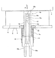
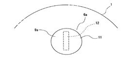
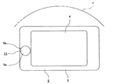
図1〜6は、本発明に関する参考例の第1例を示している。本参考例のウェアインジケータ6aは、ディスクブレーキ用のブレーキ素子であるパッド2に組み付ける事を考慮したものであって、図2〜3に示す様な支承部材11を有する。この支承部材11は、図1に示す様なセラミック製で薄肉の(例えば厚さが0.2〜0.4mm程度、より具体的には0.3mm程度の)基板12を、熱硬化性合成樹脂製のホルダ9a内に包埋支持して成る。そして、使用状態では上記支承部材11を、図4に示す様に、裏板3の片面にライニング4を添着して成るパッド2の裏板3の一部で、このライニング4の外周縁から突出する部分に、この裏板3の片面からこのライニング4を添設した側に突出する状態で装着する。
【0012】
上記基板12の片面には第一、第二両合流電路13、14を、互いに平行に設けている。そして、これら両合流電路13、14同士の間に複数本(図示の例では4本)の抵抗部22a〜22dを有する導電路15a〜15dを、それぞれの両端部を上記両合流電路13、14に導通させた状態で、互いに並列に設けている。従って、これら両合流電路13、14及び上記各導電路15a〜15dにより上記基板12の片面に、梯子形状の電路が形成される。この様な電路を構成する、上記両合流電路13、14及び上記各導電路15a〜15dは、上記基板12の片面に印刷により設けている。
【0013】
又、上記支承部材11を上記裏板3の一部に、上記図4に示す様に装着した状態で、上記各導電路15a〜15dは、上記ライニング4の厚さ方向(図1、2、5、6の上下方向、図3、4の表裏方向)に関して互いに異なる位置に、互いに並列に設置された状態となる。又、この設置状態で上記基板12の面方向が、図3に示す様にディスク1の回転方向に対し直角方向になる様に、即ち、この基板12の面方向がこのディスク1の径方向に一致する様に、上記基板12を配置している。尚、上記ホルダ9aの基端部(図2の下端部)には1対の端子16a、16bを設けており、これら両端子16a、16bの基端部を、それぞれ上記第一、第二合流電路13、14に接続すると共に、これら両端子16a、16bの中間部乃至先端部を、上記ホルダ9aの基端面から突出させている。設置状態では上記両端子16a、16bの中間部乃至先端部に、図示しない制御器に通じるハーネスの端部を接続する。
【0014】
上述の様に構成する本参考例のウェアインジケータ6aを前記パッド2に組み込むと、前記ライニング4の摩耗進行に伴って、それぞれが抵抗部22a〜22dを有する複数の導電路15a〜15dが、上記パッド2を構成する前記裏板3から遠い側から順次切断される。即ち、上記ライニング4の摩耗が進行するのに伴って、制動時に於ける前記裏板3と上記ディスク1との距離が短くなり、上記ウェアインジケータ6aを構成する支承部材11が、その先端部から基端部に向かって、上記ディスク1の側面との摩擦に基づいて次第に消失する。この場合に於いて、上記支承部材11のうちのホルダ9aは、上記ディスク1の側面との摩擦によって摩耗消失し、セラミック製の基板12が、上記ホルダ9aの先端(図2の上端)から露出した状態で折損して消失する。上記基板12を構成するセラミックはディスク1を構成する鋳鉄よりも硬い反面脆い為、この基板12を薄肉にすると共にこの基板12の面方向をこのディスク1の回転方向に対し直角に配置する事で、上記ホルダ9aの先端面から露出した上記基板12が、次々に折損する様に構成できる。尚、この基板12の折損がより確実に行なわれる様にする為、この基板12の両側縁部に、細かな切り欠きを多数形成する事もできる。
【0015】
この様にして上記基板12が先端側(図1〜2の上端側)から折損すると、この基板12の片面に配設した上記各導電路15a〜15dが、先端側の導電路15aから基端側(図1〜2の下端側)の導電路15dに向けて、順番に切断される。この様にして各導電路15a〜15dが切断されるのに伴って、上記第一合流電路13と上記第二合流電路14との間の抵抗が次第に大きくなる。従って、これら両合流電路13、14間の抵抗値の変化に対応する値に基づいて、上記ライニング4の摩耗量を、上記各導電路15a〜15dの数に合わせた段階(図示の例では4段階)で検出できる。この点に就いて、図5〜6を参照しつつ説明する。
【0016】
このうちの図5は、本参考例のウェアインジケータ6aの等価回路を、図6はこのウェアインジケータ6aを検知回路に組み込んだ状態の等価回路を、それぞれ示している。尚、この検知回路を示す図6で、Vm は上記ライニング4の摩耗に応じた出力であるモニタ電圧を、Rr はこのモニタ電圧を得る為の抵抗部(抵抗値に就いてもこの符号をそのまま使用する)を、それぞれ示している。又、このモニタ電圧を得る為の電源の電圧を5Vとした場合で説明する。
【0017】
先ず、上記各導電路15a〜15dの抵抗部22a〜22dの抵抗値をそれぞれR1 、R2 、R3 、R4 とすると、上記ライニング4が摩耗しておらず、図5〜6に示す様に総ての導電路15a〜15dが前記第一、第二合流電路13、14同士を接続している状態では、これら両合流電路13、14同士の間の抵抗値は、
1/{(1/R1 )+(1/R2 )+(1/R3 )+(1/R4 )}
となる。
そして、上記モニタ電圧Vm は、
Vm =5・Rr /[1/{(1/R1 )+(1/R2 )+(1/R3 )+(1/R4 )}]
となる。
【0018】
次に、上記ライニング4が少し摩耗し、最もディスク1寄りの導電路15aが切断されると、両合流電路13、14同士の間の抵抗値は、
1/{(1/R2 )+(1/R3 )+(1/R4 )}
となる。
そして、上記モニタ電圧Vm は、
Vm =5・Rr /[1/{(1/R2 )+(1/R3 )+(1/R4 )}]
となる。
上記ライニング4の摩耗の進行に伴って、次にディスク1に近い導電路15bが切断されると、両合流電路13、14同士の間の抵抗値は、
1/{(1/R3 )+(1/R4 )}
となる。
そして、上記モニタ電圧Vm は、
Vm =5・Rr /[1/{(1/R3 )+(1/R4 )}]
となる。
上記ライニング4の摩耗の進行に伴って、次にディスク1に近い導電路15cが切断されると、両合流電路13、14同士の間の抵抗値は、
1/(1/R4 )=R4
となる。
そして、上記モニタ電圧Vm は、
Vm =5・Rr /R4
となる。
上記ライニング4が更に摩耗し、総ての導電路15a〜15dが切断されると、両合流電路13、14同士の間の抵抗値は∞となり、上記モニタ電圧Vm は、 Vm =5・Rr /∞=0
となる。
【0019】
この様に本参考例のウェアインジケータ6aをパッド2に組み付ければ、上記ライニング4の摩耗量に応じて上記第一、第二合流電路13、14同士の間の抵抗値を1/{(1/R1 )+(1/R2 )+(1/R3 )+(1/R4 )}から∞まで、全部で5段階に変化させ、上記モニタ電圧Vm を同じく5段階に変化させる事ができる。従って、このモニタ電圧Vm を演算器を備えた制御器により処理する事で、上記ライニング4の摩耗量を、少なくとも5段階で求める事ができる。更には、このライニング4の厚さ方向に関して隣接する導電路15a〜15dが切断される間の走行距離から、走行距離と摩耗量との関係を求め、この関係とその後の走行距離とから、各時点での摩耗量を推定して表示する事も可能になる。この様に、上記ライニング4の摩耗量に関して、運転者に細かな状況を知らせる事ができる為、知識の乏しい運転者に与える不安感の軽減を図れる。又、上記ウェアインジケータ6a自体、ブレーキ素子であるパッド2からは独立したものであるから、製造は容易であり、更に、前記第一、第二両合流電路13、14を制御器に接続する等の配線は容易に行なえる。
【0020】
次に、図7は、請求項2に対応する構造の1例を示している。上述の参考例の第1例の場合、基板12を包埋して支承部材11を構成するホルダ9a(図2〜3)を円柱状に構成していたのに対して、本例の場合には、ホルダ9bを、円周方向の一部に平坦部17を形成した欠円柱状としている。そして、このホルダ9b内に包埋支持された基板12の片面に設けた第一、第二両合流電路13、14及び各導電路15a〜15d(図1参照)を、上記基板12のうちでこの平坦部17に対向する片面に設置している。尚、これら平坦部17と基板12の片面とは互いに平行にし、できるだけ近づけて、上記ホルダ9bを構成する合成樹脂のうちで上記各導電路15a〜15dを覆う部分の厚さをできるだけ薄くしている。
【0021】
この様にこれら各導電路15a〜15dを覆う合成樹脂の厚さを薄くすると、これら各導電路15a〜15dが、制動時の摩擦により温度上昇したディスク1やライニング4(図2、4、25参照)からの熱を受けて温度上昇し易くなる。この為、上記各導電路15a〜15dを、上記ディスク1やライニング4の温度検知に利用できる。即ち、これら各導電路15a〜15dとして、サーミスタ等の温度により抵抗値が変化するものを使用すれば、これら各導電路15a〜15dの両端部をそれぞれ接続した上記第一、第二両合流電路13、14同士の間の抵抗値から、上記ディスク1やライニング4部分の温度を知る事ができる。
【0022】
尚、上記各導電路15a〜15dは、上記ライニング4の摩耗の進行に伴って順番に切断される為、上記第一、第二両合流電路13、14同士の間の抵抗値は、温度変化とは別にライニング4の摩耗によっても変化する事は、前述の本発明に関する参考例の第1例で述べた通りである。そこで、本例を実施する場合には、車両の始動時等に、上記第一、第二両合流電路13、14同士の間の抵抗値と温度とを関連付ける初期設定を行なう。始動時には上記ディスク1やライニング4部分の温度は外気温と考えられるので、初期設定時に於ける抵抗値を外気温に見合う抵抗値とする。外気温を表わす信号は、空調機用の外気温センサ等から求める。尚、車両を運行停止直後に再始動する場合、上記ディスク1やライニング4部分の温度が外気温よりも高くなっているので、車両を運行停止から再始動までの時間が或る程度(例えば2時間以上)経過しない限り、上記初期設定を行なわない様にする。
【0023】
次に、図8は、本発明に関する参考例の第2例を示している。本参考例の場合には、基板12の両面にそれぞれ複数本ずつ(図示の例では4本ずつ)の導電路15a〜15d、15a´〜15d´を設けている。このうち、上記基板12の片面18{図8(A)の左面で図8(B)に表した面}に、上記各導電路15a〜15dと第一、第二両合流電路13、14とを設置している。そして、パッド2のライニング4(図2、4、25参照)の厚さ方向(図8の上下方向)に関して互いに異なる位置に(図示の例では等ピッチで)設置した上記各導電路15a〜15dの一端部を上記第一合流電路13に、他端部を第二合流電路14に、それぞれ接続している。又、上記基板12の他面19{図8(A)の右面で図8(C)に表した面}に、上記各導電路15a´〜15d´と第一、第二両合流電路13´、14´とを設置している。そして、パッド2のライニング4の厚さ方向に関して互いに異なる位置に等ピッチで設置した上記各導電路15a´〜15d´の一端部を上記第一合流電路13´に、他端部を第二合流電路14´に、それぞれ接続している。
【0024】
上記片面18に設置した第一、第二両合流電路13、14と、他面19に設置した第一、第二両合流電路13´、14´とは、互いに導通させている。この為に、上記基板12の一部で第一合流電路13、13´に整合する部分、並びに第二合流電路14、14´に整合する部分に、それぞれ通孔を形成し、これら各通孔を通じて、上記両第一合流電路13、13´同士、並びに上記両第二合流電路14、14´同士を、互いに導通させている。又、上記ライニング4の厚さ方向に関して、上記基板12の片面18に設けられた上記各導電路15a〜15dの位置と、同じく他面19に設けられた上記各導電路15a´〜15d´の位置とが互いにずれている。
【0025】
上述の様に構成する本参考例の場合、支承部材を構成する上記基板12に、上記ライニング4の厚さ方向に関する位置を互いにずらせて配置する導電路15a〜15d、15a´〜15d´の本数を多く(図示の例では8本)できて、上記ライニング4の摩耗の進行度合いを、より細かく測定できる。即ち、本例の場合にはこのライニング4の進行に伴って上記各導電路15a〜15d、15a´〜15d´が、15a→15a´→15b→15b´→15c→15c´→15d→15d´の順で順次切断される。この為、これら各導電路15a〜15d、15a´〜15d´の一端部を接続した上記第一合流電路13、13´と同じく他端部を接続した上記第二合流電路14、14´との間の抵抗値が、上記ライニング4の摩耗の進行に伴って多段階で変化する。この結果、新品時の摩耗許容厚さが5〜10mm程度しかない、小型自動車用のライニング4に関しても、上述の様に、上記ライニング4の摩耗の進行度合いを細かく測定できる。
【0026】
次に、図9〜11は、本発明に関する参考例の第3例を示している。本参考例の場合には、それぞれの片面にそれぞれ複数ずつの導電路15a〜15d、15a´〜15d´を設けた1対の基板12a、12bを有する。このうち、図9(A)に示した一方の基板12aの片面には、上記各導電路15a〜15dと第一、第二両合流電路13、14を設置している。そして、パッド2のライニング4(図2、4、25参照)の厚さ方向(図9の上下方向)に関して互いに異なる位置に等ピッチで設置した上記各導電路15a〜15dの一端部を上記第一合流電路13に、他端部を第二合流電路14に、それぞれ接続している。又、図9(B)に示した他方の基板12bの片面に、上記各導電路15a´〜15d´と第一、第二両合流電路13´、14´を設置している。そして、パッド2のライニング4の厚さ方向に関して互いに異なる位置に等ピッチで設置した上記各導電路15a´〜15d´の一端部を上記第一合流電路13´に、他端部を第二合流電路14´に、それぞれ接続している。又、上記ライニング4の厚さ方向に関して、上記一方の基板12aの片面に設けられた上記各導電路15a〜15dの位置と、同じく他方の基板12bの片面に設けられた上記各導電路15a´〜15d´の位置とは、互いにずれている。
【0027】
この様にそれぞれの片面に導電路15a〜15d、15a´〜15d´及び第一、第二両合流電路13、14、13´、14´を設けた基板12a、12bを含む支承部材は、単一のパッド2の裏板3(図2、4、25参照)に隣接して配置する他、異なるパッド2の裏板に設置する事もできる。何れの場合でも、上記一方の基板12aの片面に設けられた第一合流電路13と他方の基板12bの片面に設けられた第一合流電路13´とは互いに導通させ、同じく第二合流電路14と第二合流電路14´とは互いに導通させる。この為、上記一方の基板12aの近傍に存在するライニング4と上記他方の基板12bの近傍に存在するライニング4とが同じ速度で摩耗すれば、前述した第3例の場合と同様に、上記ライニング4の摩耗の進行度合いを細かく測定できる。或は、上記1対の基板12a、12bに設置した第一の合流電路13、13´同士、第二の合流電路14、14´同士を互いに導通させなくても、上記ライニング4のうちで上記両基板12a、12bの近傍に存在する部分が同じ速度で摩耗すれば、これら両基板12a、12bに関するモニタ電圧を、演算器を備えた制御器により処理する事により、上記ライニング4の摩耗の進行度合いを細かく測定できる。
【0028】
尚、基板12a、12bを含む支承部材を異なるパッド2の裏板に設置する態様は、各種考えられるが、次に、そのうちの2例に就いて説明する。先ず、図10に示した第1例は、単一のディスクブレーキを構成する1対の(インナ側、アウタ側両)パッド2、2に設置する状態を示している。この場合、これら両パッド2、2を構成するライニング4、4の摩耗が同じ様に進行すれば、その進行度合いを細かく測定できる。次に、図11に示した第2例の場合には、上記基板12a、12bを車両の左右に振り分けて設置したものである。この例では、図11(A)に示した左車輪用のディスクブレーキを構成するアウタ側のパッド2に一方の基板12aを、同図(B)に示した右車輪用のディスクブレーキを構成するアウタ側のパッド2に他方の基板12bを、それぞれ設置している。この設置状態の場合、これら両アウタ側のパッド2、2を構成するライニング4、4の摩耗が同じ様に進行すれば、その進行度合いを細かく測定できる。又、上記図11(A)(B)に示す、左右両車輪用のディスクブレーキには、インナ側のパッド2、2に関しても、アウタ側のパッド2、2と同様に、基板12a、12bを設置している。
【0029】
次に、図12〜13は、本発明の実施の形態の第1、2例を示している。本例の場合、各導電路20a〜20dは、良導電材製の良導電部21a〜21dと電位抵抗を有する抵抗部22a〜22dとを互いに直列に配置して成る。そして、これら各抵抗部22a〜22dを、基板12の一部で、パッド2への設置状態でライニング4の厚さ方向に関して摩擦面23(図25参照)から離れた側(図12の下側)に片寄せて設置している。この結果、上記各抵抗部22a〜22dとディスク1(図25参照)の側面との距離をできるだけ大きくすると共に互いに等しくしている。
【0030】
この様な構造を採用する事により、上記各抵抗部22a〜22dが制動時に温度上昇する上記ディスク1の熱の影響を受けにくくすると共に、受けた場合でも各抵抗部22a〜22dへの影響が等しくなる様にして、上記ライニング4の摩耗量検出の信頼性向上を図っている。尚、図12に示した第1例と、図13に示した第2例との相違点は、上記各導電路20a〜20dの形状が異なるのみである。即ち、第2例の構造は、これら各導電路20a〜20dの先端部で上記ディスク1との摩擦に伴って切断される部分の長さ寸法を短くしている。
【0031】
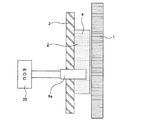
次に、上述の様な本発明のブレーキ素子用ウェアインジケータを組み込んで構成したブレーキ素子の摩耗検出装置の全体構成に就いて、図14〜19により説明する。図14は、車体の四隅に設けた4個の車輪24、24のそれぞれに、本発明のウェアインジケータ6a、6aを設けた状態を示している。これら各ウェアインジケータ6a、6aを構成する第一、第二各合流電路13、14(例えば図6参照)と演算制御器25とを、それぞれ2本ずつのハーネス26a、26bにより導通させている。
【0032】
上記演算制御器25は、図16に示す様に、演算器27と、定電圧電源回路28と、基準抵抗29とを備える。このうちの演算器27は、上記各ハーネス26a、26bを通じて送り込まれる信号、即ち、上記各ウェアインジケータ6a、6aの抵抗値に基づいて変化する電圧に基づいて、当該ウェアインジケータ6a、6aが付設されたパッド2のライニング4の摩耗量を算出する。又、上記定電圧電源回路28は、上記各ウェアインジケータ6a、6aの第一合流電路13と上記演算器27との間に一定の電圧を印加する為のものである。更に、上記基準抵抗29は、上記各ウェアインジケータ6a、6a及び定電圧電源回路28との組み合わせにより、上記演算器27に、図15に示したライニング4の摩耗量を算出させる為のモニタ電圧を得る為のものである。この様な演算器27と、定電圧電源回路28と、基準抵抗29とを備えた上記演算制御器25は、(懸架装置を基準として車輪側ではなく)車体側に設置している。
【0033】
尚、図示の例では、上記演算制御器25に、バッテリ30から電力を供給すると共に、車速センサ31からの信号を入力している。尚、この車速センサ31からの信号は、例えば制動時に上記ライニング4の摩耗量を推定する為に利用したり、このライニング4が摩耗した事を運転者に知らせる為の警報を出すタイミングを計る為に使用するが、本発明とは直接は関係しない。何れにしても、上記演算制御器25は、上記各ウェアインジケータ6a、6aの抵抗値に基づき、前記各車輪24、24毎に複数枚ずつ設けたパッド2のライニング4の摩耗状態(摩耗量)を表す信号(摩耗信号)を発すると共に、このライニング4が許容限度にまで摩耗した場合に、運転者にパッド2の交換を促す警報を発する為の信号(警報信号)を発する。
【0034】
上記各ウェアインジケータ6a、6a及び前記演算器27に対する、上記定電圧電源回路28及び上記基準抵抗29の接続状態としては、図17に示すものと図18に示すものとの2種類に大別できる。このうちの図17に示したものは、請求項4に対応する構造を有し、上記基準抵抗29を、所謂プルダウン抵抗として使用するもので、前述の図6に示した形態と同じである。この様な図17に示した構造の場合には、上記各ウェアインジケータ6a、6aを構成する導電路15a〜15dが順次切断されるのに伴って、上記演算器27に送り込まれる信号電圧(モニタ電圧Vm )が、図19(A)に示す様に順次低下する。この際の信号電圧の値は、前述の段落番号[0015]〜[0018]で説明した通りである。
【0035】
これに対して、図18に示したものは、請求項3に対応する構造を有し、上記基準抵抗29を、所謂プルアップ抵抗として使用するものである。この様な図18に示した構造の場合には、上記各ウェアインジケータ6a、6aを構成する導電路15a〜15dが順次切断されるのに伴って、上記演算器27に送り込まれる信号電圧(モニタ電圧Vm )が、図19(B)に示す様に順次上昇する。この際の信号電圧の値は、上記プルダウンの場合とは逆に変化する。この場合に就いても、上記定電圧電源回路28の電圧を5Vとし、基準抵抗29の抵抗値をRr として説明する。
【0036】
先ず、上記各ウェアインジケータ6a、6aが新品の場合に上記モニタ電圧Vm は、
Vm =5・[1/{(1/R1 )+(1/R2 )+(1/R3 )+(1/R4 )}]/[{1/((1/R1 )+(1/R2 )+(1/R3 )+(1/R4 ))}+Rr ]
となる。
次に、前記ライニング4が少し摩耗し、最もディスク1寄りの導電路15aが切断されると上記モニタ電圧Vm は、
Vm =5・[1/{(1/R2 )+(1/R3 )+(1/R4 )}]/[{1/((1/R2 )+(1/R3 )+(1/R4 ))}+Rr ]
となる。
そして上記モニタ電圧Vm は上記ライニング4の摩耗の進行に伴って、
Vm =5・[1/{(1/R3 )+(1/R4 )}]/[{1/((1/R3 )+(1/R4 ))}+Rr ]
Vm =5・{1/(1/R4 )}/[{1/(1/R4 )}+Rr ]
となる。
そして、上記ライニング4の摩耗の進行に伴って総ての導電路15a〜15dが切断されると、両合流電路13、14同士の間の抵抗値は∞となり、上記モニタ電圧Vm は、5Vとなる。
【0037】
前述の様なプルダウン、上述の様なプルアップ、何れの構造を採用する場合でも、前記演算制御器25は、前記各ウェアインジケータ6a、6aから送り込まれるモニタ電圧Vm に基づいて前記ライニング4の摩耗量を求め、前記摩耗信号や警報信号を発する。何れにしても本発明のブレーキ素子の摩耗検出装置の場合には、前記演算器27と、前記定電圧電源回路28と、前記基準抵抗29とを、車体側に設置する演算制御器25側に設けているので、これら各部材27〜29の組み付け作業を容易に行なえる。特に、請求項4に記載した様に、上記基準抵抗29と、上記各ウェアインジケータ6a、6aの第二合流電路14を上記演算器27に、直接又は上記基準抵抗29を介して導通させる為のアースとを、上記演算制御器25内に設置すれば、上記組み付け作業をより容易にできる。即ち、上記各ウェアインジケータ6a、6aと上記演算制御器25とを、単にハーネス26a、26bにより接続するのみで足りる様に(途中に部品を組み付ける事を不要に)できる。又、車両に設置する他の制御回路との間で制御基板を共用化する事により、コスト並びにスペースを節約する事もできる。
【0038】
尚、上記各ウェアインジケータ6a、6aと、上記演算器27、上記定電圧電源回路28、上記基準抵抗29を含む上記演算制御器25との接続状態は、上述した構造に限定されるものではない。要は、上記モニタ電圧Vm を得て上記ライニング4の摩耗量を求められる構造であれば、適宜変更実施する事ができる。例えば、プルダウン構造の場合には、図20〜22に示す様な構造が採用可能である。又、プルアップの場合には、図23〜24に示す様な構造が採用可能である。
【0039】
尚、図示は省略するが、本発明は、ブレーキシューアッセンブリにも適用できる。この場合には、各導電路をドラムの内周面との摩擦により切断する。
【0040】
【発明の効果】
本発明のブレーキ素子用ウェアインジケータとブレーキ素子の摩耗検出装置は、以上に述べた通り構成し作用するので、製造が容易で優れた取り扱い性を有する構造にも拘らず、ライニングの摩耗状態を複数段に分けて運転者に知らせる事ができる。この為、知識の乏しい運転者に与える不安感を軽減できる装置の低コスト化を図れる。
【図面の簡単な説明】
【図1】 本発明に関する参考例の第1例を示す、第一、第二合流電路及び導電路を設置した基板の略正面図。
【図2】 この基板をホルダにより包埋して構成したウェアインジケータの正面図。
【図3】 車両への設置状態をディスクの回転軌道との関係で示す、図2の矢印α方向に一致する、車両の幅方向外側から見た状態で示す図。
【図4】 同じくパッドへの設置状態を、図3と同方向から見た状態で示す略図。
【図5】 この基板に設置した第一、第二合流電路及び抵抗の等価回路図。
【図6】 この基板を含んで構成した摩耗検出装置の回路図。
【図7】 請求項2に対応する構造の1例を示す、ウェアインジケータの先端面図。
【図8】 本発明に関する参考例の第2例を示しており、(A)は略側面図、(B)は(A)の左方から見た図、(C)は同じく右方から見た図。
【図9】 同第3例を示しており、(A)は一方の基板の片面側から、(B)は同じく他方の基板の片面側からそれぞれ見た略正面図。
【図10】 第3例の構造の組み込み状態の第1例を示す略図。
【図11】 同第2例を示す略図。
【図12】 本発明の実施の形態の第1例を示す基板の略正面図。
【図13】 同第2例を示す基板の略正面図。
【図14】 本発明のブレーキ素子の摩耗検出装置を車両に組み付けた状態の1例を示す略平面図。
【図15】 図14のX部の要部拡大断面図。
【図16】 本発明のブレーキ素子の摩耗検出装置のブロック図。
【図17】 摩耗検出装置をプルダウン構造で構成した場合の第1例を示す要部回路図。
【図18】 同じくプルアップ構造で構成した場合の第1例を示す要部回路図。
【図19】 プルダウン構造とプルアップ構造とで、ライニングの摩耗に伴ってもモニタ電圧が変化する状態を示すグラフ。
【図20】 摩耗検出装置をプルダウン構造で構成した場合の第2例を示す要部回路図。
【図21】 同じく第3例を示す要部回路図。
【図22】 同じく第4例を示す要部回路図。
【図23】 摩耗検出装置をプルアップ構造で構成した場合の第2例を示す要部回路図。
【図24】 同じく第3例を示す要部回路図。
【図25】 ディスクブレーキの構造を示す部分略断面図。
【図26】 従来から知られているウェアインジケータ付パッドの1例を示す、部分断面図。
【符号の説明】
1 ディスク
2 パッド
3 裏板
4 ライニング
5 取付孔
6、6a ウェアインジケータ
7、7a 保持筒
8 圧縮ばね
9、9a、9b ホルダ
10 導線
11 支承部材
12、12a、12b 基板
13、13´ 第一合流電路
14、14´ 第二合流電路
15a、15b、15c、15d、15a´、15b´、15c´、15d´ 導電路
16a、16b 端子
17 平坦部
18 片面
19 他面
20a、20b、20c、20d 導電路
21a、21b、21c、21d 良導電部
22a、22b、22c、22d 抵抗部
23 摩擦面
24 車輪
25 演算制御器
26a、26b ハーネス
27 演算器
28 定電圧電源回路
29 基準抵抗
30 バッテリ
31 車速センサ[0001]
BACKGROUND OF THE INVENTION
The wear indicator for a brake element according to the present invention can be used as a brake shoe assembly for a drum brake or a pad for a disc brake, so that it can travel before the life of the brake element used for braking a vehicle such as an automobile, in other words, before replacement. In order to know the distance, this is for detecting the remaining thickness of the lining constituting the brake element. In this specification, the brake element is a generic term for a brake shoe assembly and a pad. Conversely, in this specification, the brake shoe assembly refers to a brake element for a drum brake, and the pad refers to a brake element for a disc brake.
[0002]
[Prior art]
A brake element for a vehicle is incorporated with a lining attached to a back plate. When braking, the lining is pressed against a braking rotator such as a drum or disk. For example, in the case of a disc brake, as shown in FIG. 25, the axial direction of the disc 1 with respect to a support (not shown) in which a pair of
[0003]
The
[0004]
FIG. 26 shows an example of a pad with a wear indicator described in Japanese Utility Model Laid-Open No. 5-47562, which has been considered to achieve such an object. An attachment hole 5 is formed at the end of the
[0005]
When the
[0006]
Although not shown, Japanese Patent Application Laid-Open No. 6-193660 discloses a plurality of conductors in the lining in different positions with respect to the thickness direction of the lining, so that the degree of wear of the lining is increased in a plurality of stages. A device for notifying the driver is described.
[0007]
[Problems to be solved by the invention]
In the case of the conventional structure shown in FIG. 26, although the
The wear indicator for brake elements of the present invention has been invented in view of such circumstances.
[0008]
[Means for Solving the Problems]
The wear indicator for a brake element according to the present invention includes a support member, a plurality of conductive paths, and first and second combined current paths.
Of these, the support member is supported in a state of protruding from one side of the back plate of the brake element formed by attaching a lining to one side of the back plate, and is made of an insulating material.
Each of the conductive paths is a part of the support member and is installed in parallel with each other at different positions with respect to the thickness direction of the lining, and has a resistance.
In addition, the first merge circuit is one in which one end of each conductive path is conducted.
or,The second merging electric circuit is a circuit in which the other end portions of these conductive paths are made conductive.
Each of the conductive paths is formed by arranging a good conductive portion made of a good conductive material and a resistance portion having a potential resistance in series with each other.
Further, each of the resistance portions is arranged so as to be shifted to a side away from the friction surface in the thickness direction of the lining in a part of the substrate.
[0009]
Also, the brake element wear detection device of the present invention comprises:Claim 1 or claim 2An arithmetic unit is provided for calculating the wear amount of the lining based on the described brake element wear indicator.
In addition, one of the reference resistance units for obtaining the monitor voltage is connected between the arithmetic unit and the first junction circuit or the second junction circuit of the brake element wear indicator.
Furthermore, the other end of the reference resistor is connected to a constant voltage power supply circuit for applying a constant voltage to the resistor (Claim 3in the case of).
Or, the other end of the reference resistor is connected to ground (Claim 4in the case of).
In any case, the reference resistance unit is provided in an arithmetic controller that incorporates the arithmetic unit.
[0010]
[Action]
When the wear indicator for a brake element of the present invention configured as described above is incorporated into a brake element, the plurality of conductive paths are sequentially cut from the side far from the back plate as the lining wears. As the conductive path is cut, the resistance between the first merge circuit and the second merge circuit increases. Accordingly, the brake element wear indicator is, for example,
In the case of the present invention, each resistance portion constituting each of the conductive paths is not easily affected by the heat of the disk whose temperature rises during braking, and even when received, the influence on each resistance portion is made equal. Thus, the reliability of detecting the wear amount of the lining can be improved.
[0011]
DETAILED DESCRIPTION OF THE INVENTION
1-6,Reference examples related to the present inventionA first example is shown.Reference
[0012]
On both sides of the
[0013]
Further, in a state where the
[0014]
Configure as aboveReference exampleWhen the
[0015]
When the
[0016]
Of these, Figure 5 showsReference example6 shows an equivalent circuit of the
[0017]
First, the resistance values of the
1 / {(1 / R1 ) + (1 / R2 ) + (1 / RThree ) + (1 / RFour )}
It becomes.
And the monitor voltage Vm Is
Vm = 5 ・ Rr / [1 / {(1 / R1 ) + (1 / R2 ) + (1 / RThree ) + (1 / RFour ]}]
It becomes.
[0018]
Next, when the
1 / {(1 / R2 ) + (1 / RThree ) + (1 / RFour )}
It becomes.
And the monitor voltage Vm Is
Vm = 5 ・ Rr / [1 / {(1 / R2 ) + (1 / RThree ) + (1 / RFour ]}]
It becomes.
As the wear of the
1 / {(1 / RThree ) + (1 / RFour )}
It becomes.
And the monitor voltage Vm Is
Vm = 5 ・ Rr / [1 / {(1 / RThree ) + (1 / RFour ]}]
It becomes.
As the wear of the
1 / (1 / RFour ) = RFour
It becomes.
And the monitor voltage Vm Is
Vm = 5 ・ Rr / RFour
It becomes.
When the
It becomes.
[0019]
Like thisReference exampleIf the
[0020]
Next, FIG.An example of a structure corresponding to claim 2Is shown. AboveReference exampleIn the case of the first example, the
[0021]
When the thickness of the synthetic resin covering each of the
[0022]
In addition, since each said
[0023]
Next, FIG.Second example of a reference example related to the present inventionIs shown.Reference exampleIn this case, a plurality of (four in the illustrated example)
[0024]
The first and second combined
[0025]
Configure as aboveReference exampleIn this case, the number of the
[0026]
Next, FIGS.Third example of reference example related to the present inventionIs shown.Reference exampleIn this case, a pair of
[0027]
In this way, the support member including the
[0028]
In addition, although the aspect which installs the support member containing the board |
[0029]
Next, FIGS.Of the present inventionOf the embodimentFirst and second examplesIs shown. In the case of this example, each of the
[0030]
By adopting such a structure, each of the
[0031]
Next, the overall configuration of the brake element wear detection apparatus constructed by incorporating the brake element wear indicator of the present invention as described above will be described with reference to FIGS. FIG. 14 shows a state in which the
[0032]
As shown in FIG. 16, the
[0033]
In the illustrated example, power is supplied from the
[0034]
The connection state of the constant voltage
[0035]
On the other hand, what is shown in FIG.Claim
[0036]
First, when the
Vm = 5 ・ [1 / {(1 / R1 ) + (1 / R2 ) + (1 / RThree ) + (1 / RFour )}] / [{1 / ((1 / R1 ) + (1 / R2 ) + (1 / RThree ) + (1 / RFour ))} + Rr ]
It becomes.
next,SaidWhen the
Vm = 5 ・ [1 / {(1 / R2 ) + (1 / RThree ) + (1 / RFour )}] / [{1 / ((1 / R2 ) + (1 / RThree ) + (1 / RFour ))} + Rr ]
It becomes.
And the monitor voltage Vm As the wear of the
Vm = 5 ・ [1 / {(1 / RThree ) + (1 / RFour )}] / [{1 / ((1 / RThree ) + (1 / RFour ))} + Rr ]
Vm = 5 · {1 / (1 / RFour )} / [{1 / (1 / RFour )} + Rr ]
It becomes.
When all the
[0037]
Regardless of the structure of the pull-down as described above or the pull-up as described above, the
[0038]
The connection state between the
[0039]
In addition, although illustration is abbreviate | omitted, this invention is applicable also to a brake shoe assembly. In this case, each conductive path is cut by friction with the inner peripheral surface of the drum.
[0040]
【The invention's effect】
Since the brake element wear indicator and the brake element wear detection apparatus of the present invention are configured and act as described above, a plurality of lining wear states are provided regardless of a structure that is easy to manufacture and has excellent handleability. The driver can be notified in stages. For this reason, the cost reduction of the apparatus which can reduce the anxiety given to the driver with poor knowledge can be achieved.
[Brief description of the drawings]
FIG. 1 shows the present invention.Reference examples forThe schematic front view of the board | substrate which installed the 1st, 2nd confluence | merging electric circuit and the conductive path which shows the 1st example of this.
FIG. 2 is a front view of a wear indicator configured by embedding this substrate with a holder.
3 is a diagram showing a state of installation on the vehicle in relation to the rotation trajectory of the disk, as viewed from the outside in the width direction of the vehicle, which coincides with the direction of arrow α in FIG.
4 is a schematic view showing the state of installation on the pad as seen from the same direction as FIG. 3. FIG.
FIG. 5 is an equivalent circuit diagram of the first and second junction circuits and resistors installed on the substrate.
FIG. 6 is a circuit diagram of a wear detecting device including the substrate.
[Fig. 7]An example of a structure corresponding to claim 2The tip end view of a wear indicator which shows.
[Fig. 8]Second example of a reference example related to the present invention(A) is a schematic side view, (B) is a diagram viewed from the left side of (A), and (C) is a diagram viewed from the same right side.
[Figure 9]Third example(A) is the schematic front view seen from the single side | surface side of one board | substrate, (B) is also seen from the single side | surface side of the other board | substrate similarly, respectively.
FIG. 10Third exampleThe schematic diagram which shows the 1st example of the incorporation state of the structure of.
FIG. 11 is a schematic diagram showing the second example.
FIG. 12 shows an embodiment of the present invention.First exampleThe schematic front view of the board | substrate which shows.
Fig. 13Second exampleThe schematic front view of the board | substrate which shows.
FIG. 14 is a schematic plan view showing an example of a state in which the brake element wear detection device of the present invention is assembled to a vehicle.
FIG. 15 is an enlarged cross-sectional view of a main part of an X part in FIG. 14;
FIG. 16 is a block diagram of a brake element wear detecting apparatus according to the present invention.
FIG. 17 is a main part circuit diagram showing a first example in the case where the wear detecting device is configured with a pull-down structure;
FIG. 18 is a main part circuit diagram showing a first example when similarly configured with a pull-up structure;
FIG. 19 is a graph showing a state in which the monitor voltage changes even with lining wear in the pull-down structure and the pull-up structure.
FIG. 20 is a main part circuit diagram showing a second example in the case where the wear detecting device is configured with a pull-down structure;
FIG. 21 is a main part circuit diagram showing a third example.
FIG. 22 is a main part circuit diagram showing a fourth example.
FIG. 23 is a main part circuit diagram showing a second example in the case where the wear detecting device is constituted by a pull-up structure;
FIG. 24 is a main part circuit diagram showing a third example.
FIG. 25 is a partial schematic cross-sectional view showing the structure of a disc brake.
FIG. 26 is a partial cross-sectional view showing an example of a conventionally known pad with a wear indicator.
[Explanation of symbols]
1 disc
2 pads
3 Back plate
4 Lining
5 Mounting hole
6, 6a Wear indicator
7, 7a Holding cylinder
8 Compression spring
9, 9a, 9b Holder
10 Lead wire
11 Bearing members
12, 12a, 12b substrate
13, 13 'first junction circuit
14, 14 'second junction circuit
15a, 15b, 15c, 15d, 15a ', 15b', 15c ', 15d' Conductive path
16a, 16b terminals
17 Flat part
18 single sided
19 Other side
20a, 20b, 20c, 20d Conductive path
21a, 21b, 21c, 21d Good conductive part
22a, 22b, 22c, 22d Resistor
23 Friction surface
24 wheels
25 Arithmetic controller
26a, 26b harness
27 Calculator
28 constant voltage power circuit
29 Reference resistance
30 battery
31 Vehicle speed sensor
Claims (4)
Priority Applications (1)
| Application Number | Priority Date | Filing Date | Title |
|---|---|---|---|
| JP2002119534A JP4076787B2 (en) | 2001-04-26 | 2002-04-22 | Wear indicator for brake element and wear detector for brake element |
Applications Claiming Priority (3)
| Application Number | Priority Date | Filing Date | Title |
|---|---|---|---|
| JP2001-129838 | 2001-04-26 | ||
| JP2001129838 | 2001-04-26 | ||
| JP2002119534A JP4076787B2 (en) | 2001-04-26 | 2002-04-22 | Wear indicator for brake element and wear detector for brake element |
Publications (3)
| Publication Number | Publication Date |
|---|---|
| JP2003014020A JP2003014020A (en) | 2003-01-15 |
| JP2003014020A5 JP2003014020A5 (en) | 2005-09-22 |
| JP4076787B2 true JP4076787B2 (en) | 2008-04-16 |
Family
ID=26614302
Family Applications (1)
| Application Number | Title | Priority Date | Filing Date |
|---|---|---|---|
| JP2002119534A Expired - Fee Related JP4076787B2 (en) | 2001-04-26 | 2002-04-22 | Wear indicator for brake element and wear detector for brake element |
Country Status (1)
| Country | Link |
|---|---|
| JP (1) | JP4076787B2 (en) |
Families Citing this family (2)
| Publication number | Priority date | Publication date | Assignee | Title |
|---|---|---|---|---|
| CN107531228B (en) | 2014-12-04 | 2020-06-30 | 罗伯特·博世有限公司 | Integrated wheel speed and brake pad wear monitoring system |
| KR102259264B1 (en) * | 2019-06-10 | 2021-06-01 | 김헌윤 | Brake Device for Trains |
-
2002
- 2002-04-22 JP JP2002119534A patent/JP4076787B2/en not_active Expired - Fee Related
Also Published As
| Publication number | Publication date |
|---|---|
| JP2003014020A (en) | 2003-01-15 |
Similar Documents
| Publication | Publication Date | Title |
|---|---|---|
| US7165657B2 (en) | Thin film sensor for brake lining pad wear and brake temperature sensing | |
| US4606435A (en) | Brake lining wear sensor and indicator circuit | |
| EP0337919B1 (en) | Brake block temperature and wear measuring device | |
| US9228623B2 (en) | Wear distance sensor for a brake pad of a friction brake | |
| MXPA01007311A (en) | Progressive brake lining wear sensor. | |
| US5608376A (en) | Pad wear and pad wear indicator probe | |
| CA1060560A (en) | Proportional brake lining wear sensor | |
| JPH06193660A (en) | Sensor for simultaneously detecting thickness and temperature of brake lining | |
| KR19990022383A (en) | Wear indicator of brake lining | |
| US9964168B1 (en) | Brake pad wear and temperature sensor | |
| JP4076787B2 (en) | Wear indicator for brake element and wear detector for brake element | |
| JPS6151572A (en) | Measuring device for speed of revolution | |
| JP2006526530A (en) | Brake lining wear indicator | |
| US20030006896A1 (en) | Brake wear sensor | |
| EP1399681B1 (en) | Brake lining wear system | |
| JP2002303344A (en) | Life display device of brake element for vehicle | |
| US8144003B2 (en) | Brake or clutch lining comprising a wear and tear and temperature determination unit | |
| JP6377755B2 (en) | System and method for brake sensing | |
| EP3948007B1 (en) | Unit for detecting wear and temperature of a braking member of a vehicle | |
| JPH109307A (en) | Abrasion and overheating detection device for brake lining | |
| JPH109310A (en) | Method and device for detecting brake lining abrasion | |
| FI3743636T3 (en) | Brake lining wear measuring device for a brake, brake and brake lining set | |
| JPH10252791A (en) | Abrasion alarming device for lining | |
| EP1199491A1 (en) | Block of friction material with integrated wear sensor | |
| JP2551163Y2 (en) | Brake pad with wear indicator |
Legal Events
| Date | Code | Title | Description |
|---|---|---|---|
| A521 | Written amendment |
Free format text: JAPANESE INTERMEDIATE CODE: A523 Effective date: 20050407 |
|
| A621 | Written request for application examination |
Free format text: JAPANESE INTERMEDIATE CODE: A621 Effective date: 20050407 |
|
| RD04 | Notification of resignation of power of attorney |
Free format text: JAPANESE INTERMEDIATE CODE: A7424 Effective date: 20060619 |
|
| A977 | Report on retrieval |
Free format text: JAPANESE INTERMEDIATE CODE: A971007 Effective date: 20070525 |
|
| A131 | Notification of reasons for refusal |
Free format text: JAPANESE INTERMEDIATE CODE: A131 Effective date: 20070605 |
|
| A521 | Written amendment |
Free format text: JAPANESE INTERMEDIATE CODE: A523 Effective date: 20070711 |
|
| TRDD | Decision of grant or rejection written | ||
| A01 | Written decision to grant a patent or to grant a registration (utility model) |
Free format text: JAPANESE INTERMEDIATE CODE: A01 Effective date: 20080129 |
|
| A61 | First payment of annual fees (during grant procedure) |
Free format text: JAPANESE INTERMEDIATE CODE: A61 Effective date: 20080130 |
|
| R150 | Certificate of patent or registration of utility model |
Free format text: JAPANESE INTERMEDIATE CODE: R150 |
|
| FPAY | Renewal fee payment (event date is renewal date of database) |
Free format text: PAYMENT UNTIL: 20110208 Year of fee payment: 3 |
|
| FPAY | Renewal fee payment (event date is renewal date of database) |
Free format text: PAYMENT UNTIL: 20120208 Year of fee payment: 4 |
|
| LAPS | Cancellation because of no payment of annual fees |