JP4074660B2 - Chemical sensor based on silicon - Google Patents
Chemical sensor based on silicon Download PDFInfo
- Publication number
- JP4074660B2 JP4074660B2 JP50692896A JP50692896A JP4074660B2 JP 4074660 B2 JP4074660 B2 JP 4074660B2 JP 50692896 A JP50692896 A JP 50692896A JP 50692896 A JP50692896 A JP 50692896A JP 4074660 B2 JP4074660 B2 JP 4074660B2
- Authority
- JP
- Japan
- Prior art keywords
- sensor
- chemical sensor
- sensor according
- layer
- porous
- Prior art date
- Legal status (The legal status is an assumption and is not a legal conclusion. Google has not performed a legal analysis and makes no representation as to the accuracy of the status listed.)
- Expired - Fee Related
Links
Images


Classifications
-
- G—PHYSICS
- G01—MEASURING; TESTING
- G01N—INVESTIGATING OR ANALYSING MATERIALS BY DETERMINING THEIR CHEMICAL OR PHYSICAL PROPERTIES
- G01N33/00—Investigating or analysing materials by specific methods not covered by groups G01N1/00 - G01N31/00
- G01N33/48—Biological material, e.g. blood, urine; Haemocytometers
- G01N33/50—Chemical analysis of biological material, e.g. blood, urine; Testing involving biospecific ligand binding methods; Immunological testing
- G01N33/53—Immunoassay; Biospecific binding assay; Materials therefor
- G01N33/543—Immunoassay; Biospecific binding assay; Materials therefor with an insoluble carrier for immobilising immunochemicals
-
- C—CHEMISTRY; METALLURGY
- C12—BIOCHEMISTRY; BEER; SPIRITS; WINE; VINEGAR; MICROBIOLOGY; ENZYMOLOGY; MUTATION OR GENETIC ENGINEERING
- C12Q—MEASURING OR TESTING PROCESSES INVOLVING ENZYMES, NUCLEIC ACIDS OR MICROORGANISMS; COMPOSITIONS OR TEST PAPERS THEREFOR; PROCESSES OF PREPARING SUCH COMPOSITIONS; CONDITION-RESPONSIVE CONTROL IN MICROBIOLOGICAL OR ENZYMOLOGICAL PROCESSES
- C12Q1/00—Measuring or testing processes involving enzymes, nucleic acids or microorganisms; Compositions therefor; Processes of preparing such compositions
- C12Q1/001—Enzyme electrodes
- C12Q1/002—Electrode membranes
- C12Q1/003—Functionalisation
-
- C—CHEMISTRY; METALLURGY
- C12—BIOCHEMISTRY; BEER; SPIRITS; WINE; VINEGAR; MICROBIOLOGY; ENZYMOLOGY; MUTATION OR GENETIC ENGINEERING
- C12Q—MEASURING OR TESTING PROCESSES INVOLVING ENZYMES, NUCLEIC ACIDS OR MICROORGANISMS; COMPOSITIONS OR TEST PAPERS THEREFOR; PROCESSES OF PREPARING SUCH COMPOSITIONS; CONDITION-RESPONSIVE CONTROL IN MICROBIOLOGICAL OR ENZYMOLOGICAL PROCESSES
- C12Q1/00—Measuring or testing processes involving enzymes, nucleic acids or microorganisms; Compositions therefor; Processes of preparing such compositions
- C12Q1/001—Enzyme electrodes
-
- G—PHYSICS
- G01—MEASURING; TESTING
- G01N—INVESTIGATING OR ANALYSING MATERIALS BY DETERMINING THEIR CHEMICAL OR PHYSICAL PROPERTIES
- G01N33/00—Investigating or analysing materials by specific methods not covered by groups G01N1/00 - G01N31/00
- G01N33/48—Biological material, e.g. blood, urine; Haemocytometers
- G01N33/50—Chemical analysis of biological material, e.g. blood, urine; Testing involving biospecific ligand binding methods; Immunological testing
- G01N33/53—Immunoassay; Biospecific binding assay; Materials therefor
- G01N33/543—Immunoassay; Biospecific binding assay; Materials therefor with an insoluble carrier for immobilising immunochemicals
- G01N33/54366—Apparatus specially adapted for solid-phase testing
- G01N33/54373—Apparatus specially adapted for solid-phase testing involving physiochemical end-point determination, e.g. wave-guides, FETS, gratings
- G01N33/5438—Electrodes
Abstract
Description
本発明は、トランスデューサーとして作用する半導体基板上に設けられているセンサとして働く層を備えたシリコンをベースとした化学センサに関する。
生物活性の成分で働く化学センサ公知であり、その開発は隆盛をみている。
このようなセンサは本質的に、検査すべき媒体−特に液体−に曝されるセンサとして働く物質を備えている表面層を有している。この層は、通常例えばPVCから成る膜内に固定化されて存在しているセンサとして働く物質を含んでいる。分解物質の作用の下にセンサとして働く物質から発生される信号はトランスデューサー素子により変換され、場合によっては集積されている電気処理部により最後に記録可能な形態で得られる。
トランスデューサーとしては、特に半導体電極、電界効果型トランジスタ、電位差計測型電極および電流計測型電極等が該当する。
すべての公知のセンサに共通していることは、センサ膜のその都度の基礎構造素子上への付着が大抵不十分であることである。即ち、検査すべき測定溶液が洗い流されたり、不都合な事態では直接センサ膜内に侵入してしまったり、このセンサ膜を非可逆的に損傷してしまう。これに伴って、センサ出力信号の安定性に関する問題およびドリフトに関する問題が生じる。更に、感受性の膜成分の溶液内への拡散、即ち“滲出と洗流(Ausblut und Auswaschen)”を確認しなければならない。従って、このようなセンサは寿命が限られている。更に、接触部および電子信号部が薄い固定化層によってのみ感受性の領域内から分離されており、これにより極めて故障の発生が多くなることは不利である。
このような問題を解決するための試みを、クノル氏はドイツ連邦共和国特許公開第41 15 414号公報に記載している。即ち、その記載によれば、異方性のエッチング開孔(窓)が封じ込め部(Containment)として基板内に形成され、このエッチング開孔内にセンサ膜が定着される。この閉じ込め部は非伝導性の物質で被覆されており、付加的にバイパス電極(Ableiteelektrode)が分離される。この垂直な閉じ込め部はチップ背側方向で先細りの開孔を備えており、この開孔は測定溶液と直接接触している。これにより、上に記載した欠点が回避される。特に、この技術によりいわゆる異なった物質もしくは種類の異なるイオンに対して異なった感受性を備たセンサ配列が形成される。
このセンサ様式にあっては、閉じ込め部の形成により、滲出と流出に対するイオン選択性の膜の或る程度の保護が達せられる。しかし、この技術はそれを行うには容易なことではない。即ち、この技術は経費を要するリソグラフ技術を用いて始めて実現可能である。こう言ったことから、本発明が目的とするところは、冒頭に記載の様式のセンサを、センサとして働く物質を、異なった形態で、センサの異なったタイプのトランスデューサー/電子機器に集積可能であるように、しかも故障発生率が僅かであるように、かつこの場合付加的に安定性の向上並びに感受性の増大も達せられるように構成することである。
この目的は本質的に請求の範囲請求項1に記載の様式の化学センサによって解決される。この化学センサは電子工業的に超小型化された形で得られる。
本発明による他の構成は請求の範囲の他の請求項に記載した。
本発明にあっては、多孔質の層を造る際、経費を要するリソグラフ技術の適用はしなくて済む。形成された三次元の海綿状構造は、多孔質の半導体基板内でのセンサとして働く材料の良好な機械的な定着のための、および立体的な架橋のためのマトリックスとして使用できる。これに伴い、液体中での高い物理的な(機械的な)かつ電気化学的な安定性が達せられる。従って、特に連続的な作業での使用に適しており、例えばFIA−シテムでの検出器としての使用に適している。
エッチング処理により形成された多孔質のシリコンは自体久しい以前から知られており、その使用も日本国特開昭61−218 932号に記載のバイオセンサ技術において言及されている。この公報にはISFET(イオン高感度電界効果型トランジスタ)が記載されており、このISFETの表面上にソースとドレイン間で絶縁層が形成され、次いで多結晶のシリコンで積層され、このシリコンは陽極化成処理により生化学物質のための“フイルム”として多孔質のシリコン層に変換される。この提案はバイオセンサの形態の改良に関しては明らかに全くと言っていいほど示唆するところがなく、またクノル氏の提案から推察可能であるように実際の使用に程遠い。
この日本国公開特許公報に開示の内容と本発明は、トランスデューサーとして働く半導体基板が、表面から物質内に侵入する多孔質の海綿状構造を形成するために直接エッチング処理され、この多孔質の海綿状構造の孔はセンサとして働く物質の侵入能に適合した平均孔径を有している点で異なる。
この場合、特に厚みの僅かな非伝導性の絶縁層の間挿の下にセンサとして働く物質を収容する、メソ孔および/またはマクロ孔を有している、海綿状の多孔質層が有利であり、従ってセンサとして働く物質の単位面積(幾何学的な表面)当たりの有効性は著しく増大する。
もちろん、センサとして働く物質の種類および形状により、エッチング処理により生成される多孔質のシリコンの必要とする海綿状構造が決定される。
根本的にドーピングに応じて異なる多孔質輪郭が得られ、その際n−シリコン内に枝分かれを有する深く侵入したエッチング開孔が形成され、このエッチング孔の平均孔径は選択された予備処理のパラメータ、温度、電解液の組成、陽極化成電流密度および陽極化成時間並びに後処理により決定される。陽極エッチングの処理の間の照射により開孔形成を調節することが可能であり、その際特に間欠的な光線入射により場合によっては開孔内の所望の直径の変動を全長にわたって達することが可能である。
p−シリコン並びにn+−シリコンもしくはp+−シリコンをエッチング処理することにより(マイクロ多孔質の、もしくはいわゆる矢はず張り形の枝別れ(Fischgraetenverzweigung)を備えて)形成される多孔質の構造は、積層されるセンサとして働く物質の種類に応じて使用可能である。エッチング処理とエッチング処理結果に関する詳細は、雑誌『J.Appl.Phys.』、1992年71Rlに所載のR.L.SmithとS.D.Collinsの論文に記載されている。
形成される海綿状構造の孔径により、この孔径をマクロ多孔質シリコン(<2nm)、メソ多孔質シリコン(2−50nm)とマクロ多孔質シリコン(>50nm)とに区別される。
本発明によるエッチング処理のために適用可能なプロセスパラメータを以下に記載する。
−半導体基板の電気化学的な前処理(フッ化水素酸、有機および無機溶剤、水、並びにそれらの混合物質)
−使用されるエッチング処理剤および溶剤(HF−エタノールもしくはHF−プロパノール−混合物質);
−プロセス温度(5−150℃);
−陽極化成処理電流(1−500mA/cm2);
−陽極化成処理中の付加的な照射(波長λ=200−800nm、強度および出力:0,1−100mW/cm2、照明の設置場所:試料の上側或いは試料の下側並びに照明の周波数f=0,1−1000Hz);
−多孔質の海綿状構造の後処理(洗浄レジメ、例えばエタノール中で/温度/貯蔵条件、例えばN2−雰囲気中で)。
シリコンー海綿状構造の孔壁上に形成される非伝導性の層は、自体公知の方法により(最も簡単な場合)SiO2或いはAl2O3或いはTa2O5或いはまたZrO2、Si3N4、珪酸塩、ガラス等のような他の誘電化合物−それら単独で或いは組合せで−から成る。この目的で、SiO2を使用した場合は、海綿状構造の存在しているSi−表面を酸化処理するのが有利である。これは特に、熱的な、無機的な、化学的な均一な酸化或いはまた自然の酸化により達せられる。その際、得られた非伝導性の層の層厚みは−孔の大きさに依存しているが−1−100nmの範囲で変動可能である。
Al2O3或いはTa2O5を使用した場合は、先ず基礎となる金属(AlおよびTa)は、例えば電気化学的に、直流電気により或いは気相から析出され、これに引続いて−上記のSiに関して記載したと同様にして−相当する酸化物に変換される。
SiO2、Al2O3、Ta2O5、ZrO2、Si3N4等のような酸化の誘電化合物を従来のPVD−方法およびCVDの方法により直接シリコン基板上に析出させることは公知である(雑誌『Sensor and Actuators』、17巻(1994)、157−164頁参照)。
本発明によりこのようにして形成された多孔質の構造中に或いはこの構造面に“定着される”センサとして働く物質は、大多数知られている。従って、以下に、異なったシステムとシリコンのこの目的に適切な多孔率並びに定着の例を記載する。
純粋な吸着もしくは化学吸着以外に、多孔質の構造へのセンサとして働く物質の共有結合も有利であり、この多孔質の構造の平均孔径は10〜103nmに選択される。この孔表面は、センサとして働く物質を結合するために、化学的な前処理或いは変性により、例えばシラン化により、活性化される。更に、例えばグルタルジアルデヒドのようないわゆる機能的な架橋体(スペーサ分子)が孔境界面に或いは孔壁に定着される。
孔層内に侵入した生体分子相互の、例えばグルタルジアルデヒドとの完全な或いは部分的な(例えば表面近傍の領域内においてのみの)架橋は、層内における生化学物質の特別安定した統合を誘起する。このような架橋は多孔質層内に生体分子が侵入した後、例えばグルタルジアルデヒドで飽和された雰囲気での露光により達せられる。このようにして処理される層の平均孔径は≧50nmである。
酵素、たんぱく質、抗体、細胞、細胞内小器官、組織片等のような生物学的構造体は直接或いはゲル封じ込めにより、即ちポリウレタン、ポリアクリルアミド、寒天、ゼラチン等のようなポリマーから成るキャリアマトリックス内に埋設され、場合によっては立体的に架橋されて侵入させられ、その際多孔質海綿状構造内に侵入させられる物質の大きさに応じて、平均孔大きさは10nmから100μmの範囲で、特に≧20nmに選択される。
例えば、
−PVC
−軟化剤
−イオン活性化合物(イオノフォア)
−添加剤
から成る“膜カクテル(Membrancocktail)”として使用される液状膜の形のセンサとして働く物質を定着するために、少なくとも50nm、特に100nm以上の孔大きさが適用される。
液状のゾル/ゲル層+湿潤剤として孔内に侵入させられ、引続いて焼戻されて無定形のガラス層−これは原料カクテルに依存して、例えば異なったアルカリイオンの検出に使用可能である−とされたガラス層は、特に化学センサとして適している。この場合も同様に孔の大きさが≧50nm、特に100nm以上であるのが有利である。直流電流のもしくは気体相からおよび電気化学的に多孔質物質中で析出された金属から成る固体層は、陰イオンの検出に使用できる金属化合物(例えばAg/Agcl等のような)との組合せで、所定の孔大きさに関して極めて柔軟性を有しており、この場合孔大きさが10−500nmの領域にあることが有利であることが分かった。
選択されたセンサとして働く物質は、公知の方法により異なるタイプのセンサものとの組合せで使用することが可能である。その詳細は、例えば単行本であるF.SchellerおよびF.Schubert共著“Biosesoren(バイオセンサ)”、ベルリン アカデミー出版社1989年発行を参照されたい。
上記から推察されるように、本発明の構成は極めて多様である。以下に若干の例を添付の図面を基として説明する。
第1図および第1a図 多孔質の(バイオ)化学のシリコンセンサの切断して拡大した断面図、
第2図 容量形電界効果型センサ、
第3図 電界効果センサの断面図、
第4図 電位差計測型イオン選択性電極(ISE)、
第5図 センサ配列
第1図には多孔質の(バイオ−)化学シリコンセンサの層構造が断面図で示されている。
基板2として、ドーピングされた単結晶或いは多結晶のシリコンが使用されている。ドーピングの濃度は、n−シリコンおよびp−シリコンに関して1×10¹⁴−1×1018cm3の範囲で可変され、n+−シリコンおよびp+−シリコンに関しては>1×10¹⁸/cm3である。基板2の下側には、例えばAl、Ti/Pt/Au、Cr/Sb/Au或いは類似の伝導性の化合物質のような伝導性の層もしくは層列から成るオーム背面接触層1が存在している。この接触層は、例えばPVD−析出およびイオン打込み或いは電気化学的な析出方法のような従来の積層方法により形成される。
多孔質の層構造を造るため、基板は化学的に不活性な試料小室(例えばテフロン▲R▼(米国デュポン社の商標)内に内蔵され、この試料は陽極として、エッチング液中に浸漬された(例えば白金から成る)陰極中に接続され、海綿状構造3が以下のような方法で造られる。
a)出発物質としてn−シリコンを使用した際、照射強度と照射側面に応じて異なって変成された孔構造およびチャンネル構造が得られる。光源、例えばハロゲンランプがオーム背面接触層1と反対側に存在している場合、n−シリコンの集積物中に、水平な、側方の枝別れ、いわゆる“サイドブランチ”に比される次元を備えた垂直な、マクロ孔のチャンネル3(長さは多孔質構造の層厚みに相当し、直径は0.1−10μm)が形成される。その上表面領域内に、異方性の孔構造(直径:<5nm)−この孔構造はマクロ孔の海綿状構造3との組合せで利用できるか或いはプロセス工程が終了した後NaOH−溶液で除去可能である−を備えたミクロ孔層が形成される。陽極化成電流密度(孔率の増大)も処理時間(多孔質のシリコン構造の層厚みの増大)も決定的にマクロ孔の海綿状構造の構造を決定する。このマクロ孔の海綿状構造に対して平行に形成されるミクロ孔層の層厚みは本質的に光入射深さ、即ち照射光線源の波長により決定される。
更に、照射光線源の強度を時間に依存して変更した場合、即ち孔成長の間例えば照射光線源を接続したり或いは遮断したりした場合、これに伴い付加的に垂直チャンネルの直径を変えることが可能である。照射作業相の間、遮蔽相の時間帯におけると異なる孔径が形成される。このことから、“波形の、鼓状の”かつ垂直な孔構造とチャンネル構造が得られ、これらの構造は引続いて析出するセンサ膜の機械的な定着を支援する。照射光線源がオーム背面接触層1と反対側に存在している場合、垂直なチャンネル構造の様式のマクロ孔が側方での枝別れを伴うことなく形成される。その際、プロセスパラメータに応じて、孔径は100nm〜10μmの範囲で変更可能である。この垂直なチャンネルの長さは多孔質の孔層の全層厚みの領域内にある。
b)上記の工程と異なって、n+−ドーピングされたシリコンがメソ多孔質の海綿状構造(孔径:2−50nm、チャンネル長さは多孔質構造の層厚みに相当している。)を形成する。水平な枝別れは垂直なチャンネルに対して厳格に直交して指向してはいない。多孔質層構造は“矢はず張り形状”に比される。即ち、サイドブランチは垂直なチャンネルに対して<45°の傾斜で存在している。
c)ミクロ多孔質層構造(平均孔径は<2nmである)は特にp−シリコンを介して出発物質として使用できる。この場合、異方性の、均一に分配された孔配列が形成される。孔径は上に述べた領域内において照射によって調節可能であり、孔率は陽極化成電流を変化させることにより調節可能である。
d)基礎物質としてp+−ドーピングされたシリコンを使用した場合、これによって得られる海綿状構造はn+−ドーピングされたシリコンに関して得られた結果に比される。水平な横方向枝別れは、その立体構造がb)において述べた構造に全く類似している。同様に垂直な孔径並びにチャンネル長さはその幾何学的な延長に比すことが可能である。
a)−d)に記載したような様式で色々と調節可能な海綿状構造により、センサとして働く(バイオ)化学膜の意図した調節により造ること(Tailoring)が可能となる。この目的のために、海綿状構造3は(第1a図に断面で示した)が非伝導性の物質4により積層される。このようにして形成された多孔質の層はセンサとして働く成分5を収容するのに役立つ。
その都度の使用目的に応じて、センサとして働く物質は、既に冒頭に記載したように、イオン選択性の膜として存在していることも、およびバイオセンサ素子の形でも構成されていてもよく、その際必要に応じて化学的な前処理(例えばシラン化)が行なわれ、これによりセンサ物質の多孔質の層への直接的な良好な付着および多孔質の層内への固着が可能となる:
a)イオン選択性の膜の公知の製造は同様な方法により多孔質の海綿状構造にも適用することが可能である。この目的のため、或る溶剤中に含有されている膜材料(例えばイオノフォア、軟化剤、PVC−マトリックス)が海綿状構造内に侵入させられた、この海綿状構造内で溶剤の蒸発後、安定化および固着が行なわれる。
b)更に、酵素、抗体、組織片、小器官或いはレセプターの形の生体分子をがセンサとして働く膜成分として或いは直接海綿状構造内で析出させることが可能である。これを行うには、慣用の物理的な固定化方法(例えば吸着、ゲル封じ込め)、および公知の化学的な固定化方法(例えば共有結合、架橋)も利用することが可能である。
第2図には、実施例として(バイオ)化学的な多孔質の、容量性電界効果型センサの構成が示されている。層構造は第1図に関して述べた配設に相応する。場合によっては膜の形で形成されているセンサとして働く物質6は化学センサとして、またバイオセンサとして、その都度の層組成物に応じて機能する。更に、センサとして働く物質6は海綿状構造内で、および選択的これに加えてセンサ表面6a上に析出させることが可能である。多孔質のセンサ素子は適当な(例えばテフロン或いはPMMAから成る)測定小室8に内蔵され、直接分解溶液7と接触させられる。もちろん、第3図に関連して以下に詳細に説明する基本構造に相当するカプセル化も可能である。
分解溶液7と金属性の基板接触子1間の電気的な結合を形成するために、例えば市場で手に入れることのできる電位一定なかつ分解溶液7中に入れられ基板接触子1と結合される補助電極が使用される。この補助電極の代わりに、同じ様式の非感受性のかつ多孔質のセンサ素子を補助素子として使用することも可能である。この場合、上記の配設により、一般に補助電極の大きさによって制限されるが最小化可能であると言う点で、および例えばセンサ素子および補助電極の異なっている温度係数のような外的な影響の作用が低減されと言う点で利点が得られる。
第3図には、多孔質の(バイオ)化学的電界効果型トランジスタの構造が示されている。使用それる基礎物質は上記した容量性のシリコンセンサの基礎物質に相応する。基礎物質2のドーピングに依存して、二つのポケット10−ソースとドレン−は反対のドーピングを有している。この基礎物質がn−ドーピングされている場合、ソースとドレンはp−ドーピングされ、逆となる。ソースとドレンは、金属の接触子11(例えばTi/Al、Ti/Pd/Au或いは類似の伝導性の材料)を介して固定のキャリャ、例えば伝導基板13と結合されている。金属化部11は、SiO2或いはSiO2/Si3N4或いはSiO2/Al2O3或いはSiO2/Ta2O5等から成る絶縁層もしくは絶縁層列9と9aにより基板から絶縁されて塗布されている。このような電界効果型トランジスタの製造は文献(K.Horninger著“Integrierte MOS−Schaltungen(集積されたMOS回路)”1987年、ハイデルベルク、Springer社発行)から公知になっている。
上記の配設にあって、両ポケット10間で多孔質のシリコン−ゲートの形でゲート領域を利用することは新規なことである。この目的のため、本来のプロセスの間、即ち両ポケット10のドーピング直後に、図に示したような“隆起している”ゲートが、例えば付加的なフオトリソグラフイ処理とエッチング処理とにより、造られる。このようなゲートは、選択的に半導体技術において使用される方法、例えば選択的なエピタキシー或いは類似の方法により形成することが可能である。
シリコン出発物質内での海綿状構造3の形成、或いは次いでこれに引続いて行なわれるセンサとして働く物質6の析出は、第1図に関して説明したと全く同じ方法で行なわれる。基礎キャリヤ13に対している基板接触部1は伝導性の接着結合部14により、例えば伝導性銀により形成される。センサ構造素子は、例えばエポキシ樹脂或いは他の鋳造物質から成る保護層12により測定環境から保護されており、従ってセンサとして働くゲート領域のみが分解液と接触する。しかし、カプセル化は、第2図に関連して記載した固定試料小室内への内蔵によっても行われる。容量性の多孔質の(バイオ)化学センサにおけると同様に、外的な補助電極の代わりに、非感受性のセンサ素子を使用することの可能性は、この構造によっても補助トランジスタの形でも解決可能である。
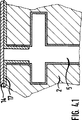
多孔質の、電位(バイオ)化学“イオン選択性電極“(ISE)の実施例は第4図から明らかである。多孔質の海綿状構造の製造とこの海綿状構造の非伝導性の物質での被覆は、第1図に関して説明したと全く同じ方法で行なわれる。この工程に引続いて、基板2は基板1の試料背壁から湿式化学的に、例えばHF/水−混合物により海綿状構造の領域内に達するまでエッチング処理により取去られる。これにより試料背壁に海綿状構造が露出する。
固形の電解液もしくは液状の電解液としてセンサとして働く成分6を、第1図に関して説明したと全く同じ方法で、海綿状構造内に侵入させられる以前に、第4.1図および第4.2図から認められるように、金属の導出部が形成されなければならない。この目的のため、第4.1図においては金属フイルム17、例えばAgから成るフイルムが従来のPVD−方法(例えば蒸着)により孔構造内に析出される。このAg層の公知の電気化学的な方法による塩化物による処理は上記の工程に直ぐ続いて行なわれる。付加的な内部電解液18は第4.2図において侵入させられる。この内部電解液は一般に高モルの塩溶液、例えば飽和KCl−溶液から成り、溶剤の蒸発の後固形有機マトリックス内に内部電解液として残る。
このようにプロセス化された半導体構造は伝導性の接着剤14、例えば伝導性銀により、例えばガラス、合成樹脂、シリコン或いはセラミック材料から成る電気的な接触層を備えたキャリア16(第4図参照)上に固定される。これによりこのキャリア16上の薄い多孔質のシリコン構造が安定される。センサとして働く層のプロセス化は、既に第1図において述べたようにして行なわれる。仕上げられた多孔質のISEは耐溶液性の材料から成る保持体15に電気的な接触部、例えばテフロン或いは合成樹脂で載置される。センサ構成素子は、例えばエポキシ樹脂或いは他の鋳造材料から成る保護層12により、この多孔質のISEのセンサとして働く領域のみが分析溶液と接触するように測定環境に対して保護されている。
第5図には、センサ配列の様式のマルチセンサとしての多孔質の(バイオ)化学半導体センサの配設が示されている。この場合、一つのシリコン基板2内に感受性でかつ多孔質の異なったセンサ19が示されている。これを形成する目的で、第一の段階として、簡単なフオトリソグラフ工程による構造形成を経て、多数のセンサ素子(例えば四つの可変のセンサ)が固定される。この工程に引続いて、その数に相当する単個の多孔質の海綿状構造が製造され、上記したプロセス工程でセンサ素子に構築される。それぞれの使用目的に応じて、第2図、第3図、第4図に関して説明したセンサ素子を形成することが可能である。これらのセンサ素子は適当な方法により試料小室に内蔵するか、或いは固定ハウジング内に収納される。The present invention relates to a silicon-based chemical sensor with a layer serving as a sensor provided on a semiconductor substrate acting as a transducer .
Chemical sensors that work with biologically active components are known and their development is flourishing.
Such a sensor essentially has a surface layer with a substance that acts as a sensor that is exposed to the medium to be examined, in particular a liquid. This layer contains a substance that acts as a sensor, usually present immobilized in a membrane made of PVC, for example. The signal generated from the substance acting as a sensor under the action of the decomposing substance is converted by a transducer element and possibly obtained in a form that can be finally recorded by an integrated electrical processing unit.
Examples of the transducer include a semiconductor electrode, a field effect transistor, a potential difference measuring electrode, a current measuring electrode, and the like .
Common to all known sensors is that the adhesion of the sensor film onto the respective substructure element is usually insufficient. That is, the measurement solution to be inspected is washed away, or in an unfavorable situation, it directly enters the sensor film, or the sensor film is irreversibly damaged. Along with this, problems related to the stability of the sensor output signal and problems related to drift arise. Furthermore, the diffusion of sensitive membrane components into the solution, i.e. "Ausblut und Auswaschen", must be confirmed. Therefore, such sensors have a limited life. Furthermore, it is disadvantageous that the contact part and the electronic signal part are separated from the sensitive area only by a thin immobilization layer, which leads to a very high number of failures.
An attempt to solve such a problem is described by Mr. Knorr in German Patent Publication No. 41 15 414. That is, according to the description, an anisotropic etching opening (window) is formed in the substrate as a containment, and the sensor film is fixed in the etching opening. The confinement part is covered with a non-conductive substance, and the bypass electrode (Ableiteelektrode) is additionally separated. This vertical confinement part has a taper opening in the direction of the back of the chip, and this opening is in direct contact with the measurement solution. This avoids the disadvantages described above. In particular, this technique forms sensor arrays with different sensitivities to so-called different substances or different types of ions.
In this sensor format, the formation of the confinement provides some protection of the ion selective membrane against leaching and outflow. But this technique is not easy to do. That is, this technique can only be realized using expensive lithographic techniques. Since saying, when the present invention is intended is a sensor of the described modes at the beginning, a substance that acts as a sensor, in different forms, it can be integrated to the transducer / electronics different types of sensors In other words, the configuration is such that the failure occurrence rate is small and, in this case, an improvement in stability and an increase in sensitivity can also be achieved.
This object is solved essentially by a chemical sensor in the manner of claim 1. This chemical sensor is obtained in a miniaturized form in the electronics industry.
Other configurations according to the invention are described in the other claims.
In the present invention, it is not necessary to apply an expensive lithographic technique when creating a porous layer . The formed three-dimensional spongy structure can be used as a matrix for good mechanical anchoring of the material acting as a sensor in the porous semiconductor substrate and for steric crosslinking. Along with this, high physical (mechanical) and electrochemical stability in the liquid is achieved. It is therefore particularly suitable for use in continuous work, for example as a detector in FIA-systems.
Porous silicon formed by etching has been known for a long time, and its use is also mentioned in the biosensor technology described in Japanese Patent Application Laid-Open No. 61-218932. This publication describes an ISFET (Ion High Sensitivity Field Effect Transistor). An insulating layer is formed between the source and drain on the surface of the ISFET, and then laminated with polycrystalline silicon. It is converted into a porous silicon layer as a “film” for biochemicals by chemical conversion treatment. This proposal clearly does not suggest any improvement in the form of biosensors, and is far from practical use, as can be inferred from Mr. Knorr's proposal.
The contents disclosed in this Japanese patent publication and the present invention are such that a semiconductor substrate acting as a transducer is directly etched to form a porous spongy structure that penetrates into the material from the surface. The pores of the spongy structure are different in that they have an average pore size adapted to the penetration ability of the substance acting as a sensor .
In this case, a spongy porous layer having mesopores and / or macropores, which contains a substance acting as a sensor under the interposition of a non-conductive insulating layer with a small thickness, is particularly advantageous. Thus, the effectiveness per unit area (geometric surface) of the substance acting as a sensor is significantly increased.
Of course, the spongy structure required for the porous silicon produced by the etching process is determined by the type and shape of the substance serving as the sensor.
Depending on the doping, different porous contours are obtained, which result in the formation of deeply penetrating etching apertures with branching in the n-silicon, the average pore diameter of which is the parameter of the selected pretreatment, It is determined by temperature, electrolyte composition, anodizing current density and anodizing time, and post-treatment. It is possible to adjust the formation of apertures by irradiation during the anodic etching process, and in particular, by intermittent light incidence, the desired diameter variation in the apertures can be reached over the entire length. is there.
Porous structures formed by etching p-silicon and n + -silicon or p + -silicon (with microporous or so-called Fischgraetenverzweigung) are: It can be used according to the type of substance that acts as a sensor to be laminated. For details on the etching process and the etching process result, see the journal “J. Appl. Phys. , 1992 71 Rl. L. Smith and S.M. D. It is described in the Collins paper.
Depending on the pore size of the spongy structure to be formed, this pore size is distinguished into macroporous silicon (<2 nm), mesoporous silicon (2-50 nm) and macroporous silicon (> 50 nm).
The process parameters applicable for the etching process according to the invention are described below.
-Electrochemical pretreatment of semiconductor substrates (hydrofluoric acid, organic and inorganic solvents, water, and mixtures thereof)
-Etching agents and solvents used (HF-ethanol or HF-propanol-mixed material);
-Process temperature (5-150 ° C);
- anodizing current (1-500mA / cm 2);
-Additional irradiation during the anodizing treatment (wavelength λ = 200-800 nm, intensity and power: 0, 1-100 mW / cm 2 , location of illumination: above sample or below sample and illumination frequency f = 0, 1-1000 Hz);
- a porous spongy structure of the post-processing (cleaning regime, for example in ethanol / temperature / storage conditions, for example N 2 - atmosphere).
The nonconductive layer formed on the pore wall of the silicon-sponge structure is formed by a method known per se (in the simplest case) SiO 2, Al 2 O 3, Ta 2 O 5, or ZrO 2 , Si 3 N. 4. Consists of other dielectric compounds such as silicates, glasses, etc.-alone or in combination. For this purpose, when SiO 2 is used, it is advantageous to oxidize the Si-surface on which the spongy structure is present. This is achieved in particular by thermal, inorganic, chemical homogeneous oxidation or also natural oxidation. At that time, the thickness of the obtained non-conductive layer depends on the size of the pores, but can be varied in the range of −1 to 100 nm.
When using Al 2 O 3 or Ta 2 O 5 , the base metals (Al and Ta) are first deposited, for example electrochemically, by direct current or from the gas phase, and subsequently-above In the same way as described for Si—converted to the corresponding oxide.
It is known to deposit an oxide dielectric compound such as SiO 2 , Al 2 O 3 , Ta 2 O 5 , ZrO 2 , Si 3 N 4 directly on a silicon substrate by conventional PVD-method and CVD method. Yes (magazine "Sensor and Actuators", 17 (1994), pp. 157-164).
Many substances are known which serve as sensors which are “fixed” in or on the porous structure thus formed according to the invention. Thus, the following describes examples of porosity and fusing appropriate for this purpose for different systems and silicon.
Besides pure adsorption or chemisorption, covalent attachment of a substance to act as a sensor to a structure of the porous also be advantageous, the average pore size of the structure of the porous is selected 10 to 10 3 nm. This pore surface is activated by chemical pretreatment or modification, for example by silanization, to bind substances acting as sensors. Furthermore, a so-called functional cross-linked product (spacer molecule) such as glutardialdehyde is fixed on the pore boundary surface or on the pore wall.
Full or partial cross-linking of biomolecules that have penetrated into the pore layer, eg with glutardialdehyde (eg only in the region near the surface) , induces a particularly stable integration of biochemicals in the layer To do . Such cross-linking is achieved by exposure in an atmosphere saturated with glutardialdehyde, for example, after a biomolecule has entered the porous layer. The average pore size of the layer treated in this way is ≧ 50 nm.
Biological structures such as enzymes, proteins, antibodies, cells, organelles, debris, etc. can be directly or by gel containment, ie in a carrier matrix consisting of polymers such as polyurethane, polyacrylamide, agar, gelatin, etc. embedded in, and in some cases allowed to penetrate are sterically crosslinking, according to the size of the case is caused to penetrate into the porous spongy structure in substance, the average pore size is in the range of 10nm to 100 [mu] m, in particular ≧ 20 nm is selected.
For example,
-PVC
-Softener-Ion active compound (ionophore)
A pore size of at least 50 nm, in particular 100 nm or more, is applied in order to fix substances that act as sensors in the form of liquid membranes used as “Membrancocktail” of additives.
Liquid sol / gel layer + wetting agent penetrated into the pores and subsequently tempered and amorphous glass layer- depending on the raw material cocktail , it can be used , for example, to detect different alkali ions A glass layer that is considered to be certain is particularly suitable as a chemical sensor. In this case as well, the pore size is advantageously ≧ 50 nm, in particular 100 nm or more. A solid layer consisting of a metal deposited from a direct current or gas phase and electrochemically in a porous material in combination with a metal compound (such as Ag / Agcl etc.) that can be used for the detection of anions. It has been found that it is very flexible with respect to a given pore size, in which case it is advantageous for the pore size to be in the region of 10-500 nm.
Substance acting as the selected sensor can be used in combination with different types of sensors ones by known methods. The details are, for example, F. Scheller and F.M. See also “Biosesoren” by Schubert, published by Berlin Academy Publishers, 1989.
As can be inferred from the above, the configuration of the present invention is extremely diverse. Some examples will be described below with reference to the accompanying drawings.
1 and 1a are cross-sectional views of a porous (bio) chemical silicon sensor cut and enlarged,
Fig. 2 Capacitive field effect sensor,
FIG. 3 is a sectional view of a field effect sensor,
Fig. 4 Potentiometric ion selective electrode (ISE),
Fig. 5 Sensor arrangement Fig. 1 shows in cross section the layer structure of a porous (bio-) chemical silicon sensor.
As the
In order to create a porous layer structure, the substrate is embedded in a chemically inert sample chamber (for example, Teflon® (trademark of DuPont, USA), and this sample was immersed in an etching solution as an anode. Connected in a cathode (for example made of platinum), a spongy structure 3 is made in the following manner.
a) When n-silicon is used as a starting material, pore structures and channel structures modified differently depending on irradiation intensity and irradiation side surface are obtained. If a light source, for example a halogen lamp, is present on the side opposite to the ohmic back contact layer 1, the dimension in the n-silicon stack is compared to a horizontal, lateral branch, the so-called “side branch”. The provided vertical macroporous channel 3 (the length corresponds to the layer thickness of the porous structure and the diameter is 0.1-10 μm) is formed. In addition, in the surface area, an anisotropic pore structure (diameter: <5 nm)-this pore structure can be used in combination with macroporous sponge-like structure 3 or removed with NaOH-solution after the process steps have been completed. A microporous layer with-is possible. (Increased porosity) anodization current density processing time (increase in the layer thickness of the silicon structure of the porous) also determines the structure of the spongy structure of the critically macropores. The layer thickness of the microporous layer formed parallel to the macroporous spongy structure is essentially determined by the light incident depth, that is, the wavelength of the irradiation light source.
Furthermore, if the intensity of the irradiation light source is changed in a time-dependent manner, i.e. if the irradiation light source is connected or disconnected during hole growth, for example, the diameter of the vertical channel is additionally changed accordingly. Is possible. During the irradiation work phase, a different pore size is formed in the shielding phase time zone. This results in “corrugated, drum-shaped” and vertical hole and channel structures, which support the mechanical anchoring of subsequently deposited sensor films. When the irradiation light source is present on the side opposite to the ohmic back contact layer 1, macrochannels in the form of vertical channel structures are formed without lateral branching. At that time, the pore diameter can be changed in the range of 100 nm to 10 μm according to the process parameters. The length of this vertical channel is in the region of the total thickness of the porous pore layer.
b) Unlike the above steps, n + -doped silicon forms a mesoporous sponge structure (pore size: 2-50 nm, channel length corresponds to the layer thickness of the porous structure). To do. The horizontal branching is not oriented strictly orthogonal to the vertical channel. The porous layer structure is compared to the “arrow-strung shape”. That is, the side branch is present at an inclination of <45 ° with respect to the vertical channel.
c) Microporous layer structures (average pore size <2 nm) can be used as starting materials, especially via p-silicon. In this case, an anisotropic, uniformly distributed hole array is formed. The pore size can be adjusted by irradiation within the region described above, and the porosity can be adjusted by changing the anodizing current.
d) If p + -doped silicon is used as the base material, the resulting spongy structure is compared to the results obtained for n + -doped silicon. The horizontal lateral branching is quite similar in structure to that described in b). Similarly, the vertical hole diameter as well as the channel length can be compared to its geometric extension.
A sponge-like structure that can be adjusted in various ways in the manner described in a) to d) makes it possible to tailor with the intended adjustment of the (bio) chemical membrane acting as a sensor. For this purpose, the spongy structure 3 (shown in section in FIG. 1 a) is laminated with a non-conductive substance 4. The porous layer thus formed serves to contain the
Depending on the intended use, the substance acting as a sensor may already exist as an ion-selective membrane as described at the beginning, and may also be configured in the form of a biosensor element, In this case, chemical pretreatment (eg silanization) is carried out if necessary, which makes it possible to adhere the sensor substance directly to the porous layer and to fix it in the porous layer. :
a) The known production of ion-selective membranes can be applied to porous spongy structures in a similar manner. For this purpose, membrane materials (eg ionophores, softeners, PVC-matrix) contained in a solvent are allowed to penetrate into the sponge-like structure, which is stable after evaporation of the solvent in the sponge-like structure. And fixing.
b) Furthermore, it is possible to deposit biomolecules in the form of enzymes, antibodies, tissue fragments, organelles or receptors as membrane components that act as sensors or directly within the spongy structure. To do this, conventional physical immobilization methods (eg adsorption, gel containment) and known chemical immobilization methods (eg covalent bonding, cross-linking) can also be used.
FIG. 2 shows the configuration of a (bio) chemical porous capacitive field effect sensor as an example. The layer structure corresponds to the arrangement described with reference to FIG. In some cases, the substance 6 acting as a sensor in the form of a membrane functions as a chemical sensor and as a biosensor, depending on the layer composition in each case. Furthermore, the substance 6 acting as a sensor can be deposited in the spongy structure and optionally in addition to the sensor surface 6a. The porous sensor element is contained in a suitable measuring chamber 8 (eg made of Teflon or PMMA) and is brought into direct contact with the decomposition solution 7. Of course, an encapsulation corresponding to the basic structure described in detail below in connection with FIG. 3 is also possible.
In order to form an electrical connection between the decomposition solution 7 and the metallic substrate contact 1, for example, it is placed in the decomposition solution 7 with a constant potential that can be obtained on the market and is connected to the substrate contact 1. An auxiliary electrode is used. Instead of this auxiliary electrode, it is also possible to use an insensitive and porous sensor element in the same manner as an auxiliary element. In this case, the above arrangement is generally limited by the size of the auxiliary electrode but can be minimized, and external influences such as different temperature coefficients of the sensor element and the auxiliary electrode, for example. An advantage can be obtained in that the action of is reduced.
FIG. 3 shows the structure of a porous (bio) chemical field effect transistor. The basic material used corresponds to the basic material of the capacitive silicon sensor described above. Depending on the doping of the
In the above arrangement, it is novel to use the gate region in the form of a porous silicon-gate between both pockets 10. For this purpose, during the original process, i.e. immediately after the doping of both pockets 10, a “raised” gate as shown in the figure is produced, for example by means of an additional photolithographic process and an etching process. It is done. Such gates can be formed by methods selectively used in semiconductor technology, such as selective epitaxy or similar methods.
The formation of the spongy structure 3 in the silicon starting material or the subsequent deposition of the material 6 acting as a sensor is carried out in exactly the same way as described with reference to FIG. The substrate contact portion 1 with respect to the
Porous, examples of potential (bio) chemical "ion selective electrode" (ISE) is clear from Figure 4. The production of the porous spongy structure and the coating of the spongy structure with a nonconductive material are carried out in exactly the same manner as described with reference to FIG. Subsequent to this step, the
Before the component 6 acting as a sensor as a solid or liquid electrolyte is introduced into the spongy structure in exactly the same manner as described with reference to FIG. 1, FIGS. 4.1 and 4.2. As can be seen from the figure, a metal outlet must be formed. For this purpose, in FIG. 4.1, a
The semiconductor structure thus processed has a carrier 16 (see FIG. 4) with an electrically contact layer made of, for example, glass, synthetic resin, silicon or ceramic material, with a
FIG. 5 shows the arrangement of a porous (bio) chemical semiconductor sensor as a multi-sensor in the form of a sensor array . In this case, different
Claims (16)
Applications Claiming Priority (3)
| Application Number | Priority Date | Filing Date | Title |
|---|---|---|---|
| DE4427921A DE4427921C2 (en) | 1994-08-06 | 1994-08-06 | Chemical sensors, especially biosensors, based on silicon |
| DE4427921.3 | 1994-08-06 | ||
| PCT/DE1995/001056 WO1996005512A1 (en) | 1994-08-06 | 1995-08-04 | Chemical sensors, in particular silicon-based biosensors |
Publications (2)
| Publication Number | Publication Date |
|---|---|
| JPH10504388A JPH10504388A (en) | 1998-04-28 |
| JP4074660B2 true JP4074660B2 (en) | 2008-04-09 |
Family
ID=6525114
Family Applications (1)
| Application Number | Title | Priority Date | Filing Date |
|---|---|---|---|
| JP50692896A Expired - Fee Related JP4074660B2 (en) | 1994-08-06 | 1995-08-04 | Chemical sensor based on silicon |
Country Status (8)
| Country | Link |
|---|---|
| US (1) | US5874047A (en) |
| EP (1) | EP0775314B1 (en) |
| JP (1) | JP4074660B2 (en) |
| KR (1) | KR100379663B1 (en) |
| AT (1) | ATE271223T1 (en) |
| CA (1) | CA2196895A1 (en) |
| DE (2) | DE4427921C2 (en) |
| WO (1) | WO1996005512A1 (en) |
Families Citing this family (53)
| Publication number | Priority date | Publication date | Assignee | Title |
|---|---|---|---|---|
| DE19608688C2 (en) * | 1996-01-02 | 1999-03-25 | Rudolf H Dr Dittel | Determination system for the immediate qualitative and quantitative, quasi-time delay free, highly specific detection of antibody-antigen reactions by electrical measurement of specific changes of relevant parameters of the surface conductivity in ultra-narrow pores in synthetic nuclear membranes |
| DE19608428C2 (en) * | 1996-03-05 | 2000-10-19 | Forschungszentrum Juelich Gmbh | Chemical sensor |
| DE19631530C2 (en) * | 1996-07-23 | 2000-03-09 | Inst Chemo Biosensorik | Ion selective sensor |
| AUPO717197A0 (en) | 1997-06-04 | 1997-07-03 | Australian Membrane And Biotechnology Research Institute | Improved biosensor |
| US6028773A (en) * | 1997-11-14 | 2000-02-22 | Stmicroelectronics, Inc. | Packaging for silicon sensors |
| GB9808264D0 (en) | 1998-04-17 | 1998-06-17 | Imperial College | Biochemical devices and their methods of manufacture |
| WO2000003230A1 (en) | 1998-07-10 | 2000-01-20 | Iatroquest Corporation | Photoluminescent semiconductor materials |
| US6762057B1 (en) * | 1998-10-23 | 2004-07-13 | Micron Technology, Inc. | Separation apparatus including porous silicon column |
| US7115422B1 (en) * | 1998-10-23 | 2006-10-03 | Micron Technology, Inc. | Separation apparatus including porous silicon column |
| EP1085320A1 (en) * | 1999-09-13 | 2001-03-21 | Interuniversitair Micro-Elektronica Centrum Vzw | A device for detecting an analyte in a sample based on organic materials |
| EP1085319B1 (en) * | 1999-09-13 | 2005-06-01 | Interuniversitair Micro-Elektronica Centrum Vzw | A device for detecting an analyte in a sample based on organic materials |
| US6405066B1 (en) * | 2000-03-17 | 2002-06-11 | The Regents Of The University Of California | Implantable analyte sensor |
| CA2406814A1 (en) * | 2000-03-17 | 2001-09-20 | F. Hoffmann-La Roche Ag | Implantable analyte sensor |
| AU2001249437A1 (en) * | 2000-03-24 | 2001-10-08 | Lyles, Mark B | Diagnostic devices containing porous material |
| EP1287345A2 (en) * | 2000-05-18 | 2003-03-05 | Medtronic, Inc. | Ion-selective solid-state polymeric membrane electrodes |
| US20040014240A1 (en) * | 2000-07-06 | 2004-01-22 | Keigo Takeguchi | Molecule detecting sensor |
| US8372139B2 (en) | 2001-02-14 | 2013-02-12 | Advanced Bio Prosthetic Surfaces, Ltd. | In vivo sensor and method of making same |
| AT410223B (en) | 2001-08-09 | 2003-03-25 | Adlassnig Alexander Mag Dr | BIOSENSORS IN THICK FILM TECHNOLOGY |
| GB0120202D0 (en) * | 2001-08-18 | 2001-10-10 | Psimedica | Body fluid collection and analysis |
| US10539561B1 (en) * | 2001-08-30 | 2020-01-21 | Customarray, Inc. | Enzyme-amplified redox microarray detection process |
| DE10145701A1 (en) * | 2001-09-17 | 2003-04-10 | Infineon Technologies Ag | Fluorescence biosensor chip and fluorescence biosensor chip arrangement |
| WO2003074548A2 (en) * | 2001-11-07 | 2003-09-12 | Auburn University | Phage ligand sensor devices and uses thereof |
| US20050112652A1 (en) * | 2002-04-19 | 2005-05-26 | Infineon Technologies Ag | Device and method for detecting biochemical reactions and/or bindings |
| DE10217569A1 (en) * | 2002-04-19 | 2003-11-13 | Infineon Technologies Ag | Device based on partially oxidized porous silicon |
| DE10217568A1 (en) * | 2002-04-19 | 2003-11-13 | Infineon Technologies Ag | Waveguides in porous substrates |
| US7361313B2 (en) * | 2003-02-18 | 2008-04-22 | Intel Corporation | Methods for uniform metal impregnation into a nanoporous material |
| DE10334097A1 (en) * | 2003-07-25 | 2005-02-24 | Hahn-Meitner-Institut Berlin Gmbh | Preparation of layers on a semiconductor surface, for use as a biosensor, uses a medium containing an organic substance against the substrate for an electrical voltage to give organic deposits on the surface as an organic layer |
| JP4250481B2 (en) * | 2003-08-11 | 2009-04-08 | キヤノン株式会社 | Porous structure |
| JP4438049B2 (en) * | 2003-08-11 | 2010-03-24 | キヤノン株式会社 | Field effect transistor, sensor using the same, and manufacturing method thereof |
| US7382004B2 (en) * | 2003-11-25 | 2008-06-03 | Sensor Electronic Technology, Inc. | Semiconductor sensing device |
| WO2005073705A1 (en) | 2004-01-29 | 2005-08-11 | Siemens Aktiengesellschaft | Electrochemical transducer array and the use thereof |
| DE102004018846A1 (en) * | 2004-04-19 | 2005-11-10 | Infineon Technologies Ag | Partially oxidized macroporous silicon with non-contiguous silicon walls |
| ATE532058T1 (en) | 2004-05-17 | 2011-11-15 | Medtronic Inc | POINT-OF-CARE HEPARIN DETERMINATION SYSTEM |
| WO2006037527A1 (en) * | 2004-09-30 | 2006-04-13 | Pamgene Bv | Masked solid porous supports allowing fast and easy reagent exchange to accelerate electrode-based microarrays |
| US20060102471A1 (en) | 2004-11-18 | 2006-05-18 | Karl Maurer | Electrode array device having an adsorbed porous reaction layer |
| US20070034513A1 (en) | 2005-03-25 | 2007-02-15 | Combimatrix Corporation | Electrochemical deblocking solution for electrochemical oligomer synthesis on an electrode array |
| US9394167B2 (en) | 2005-04-15 | 2016-07-19 | Customarray, Inc. | Neutralization and containment of redox species produced by circumferential electrodes |
| DE102005044522B4 (en) * | 2005-09-16 | 2010-02-11 | Schott Ag | Method for applying a porous glass layer, and composite material and its use |
| US20070065877A1 (en) | 2005-09-19 | 2007-03-22 | Combimatrix Corporation | Microarray having a base cleavable succinate linker |
| JP2007197297A (en) * | 2005-12-27 | 2007-08-09 | Canon Inc | Porous material, composition containing porous material, and sensor with porous material |
| US10914698B2 (en) | 2006-11-16 | 2021-02-09 | General Electric Company | Sensing method and system |
| US9536122B2 (en) | 2014-11-04 | 2017-01-03 | General Electric Company | Disposable multivariable sensing devices having radio frequency based sensors |
| US9589686B2 (en) * | 2006-11-16 | 2017-03-07 | General Electric Company | Apparatus for detecting contaminants in a liquid and a system for use thereof |
| US9538657B2 (en) | 2012-06-29 | 2017-01-03 | General Electric Company | Resonant sensor and an associated sensing method |
| US9658178B2 (en) | 2012-09-28 | 2017-05-23 | General Electric Company | Sensor systems for measuring an interface level in a multi-phase fluid composition |
| WO2011090793A2 (en) | 2010-01-20 | 2011-07-28 | Customarray, Inc. | Multiplex microarray of serially deposited biomolecules on a microarray |
| US8542023B2 (en) | 2010-11-09 | 2013-09-24 | General Electric Company | Highly selective chemical and biological sensors |
| TWI515431B (en) * | 2011-08-05 | 2016-01-01 | Univ Chang Gung | A single-use polyisopropylacrylamide colloid is used as a biological detection method for the enzyme-embedding material and a biological detector |
| DE112013004129T5 (en) | 2012-08-22 | 2015-05-21 | General Electric Company | Wireless system and method for measuring an operating condition of a machine |
| US10598650B2 (en) | 2012-08-22 | 2020-03-24 | General Electric Company | System and method for measuring an operative condition of a machine |
| US10684268B2 (en) | 2012-09-28 | 2020-06-16 | Bl Technologies, Inc. | Sensor systems for measuring an interface level in a multi-phase fluid composition |
| US9206523B2 (en) * | 2012-09-28 | 2015-12-08 | Intel Corporation | Nanomachined structures for porous electrochemical capacitors |
| CN106290483B (en) * | 2016-07-29 | 2018-12-14 | 江苏大学 | Super hydrophilic bionical water content of substrate sensor of one kind and preparation method thereof |
Family Cites Families (8)
| Publication number | Priority date | Publication date | Assignee | Title |
|---|---|---|---|---|
| JPS61218933A (en) * | 1985-03-25 | 1986-09-29 | Matsushita Electric Ind Co Ltd | Production of oxygen concentration sensor |
| JPS61218932A (en) * | 1985-03-26 | 1986-09-29 | Toko Inc | Ion high sensitivity electric field effect transistor and its manufacture |
| JPS6283641A (en) * | 1985-10-08 | 1987-04-17 | Sharp Corp | Sensor element |
| US5111221A (en) * | 1988-05-13 | 1992-05-05 | United States Of America As Represented By The Secretary Of The Navy | Receptor-based sensor |
| ATE110110T1 (en) * | 1989-04-04 | 1994-09-15 | Pittner Fritz | METHODS FOR IMMOBILIZING PROTEINS, PEPTIDES, COENZYMES OR THE LIKE. ON A CARRIER. |
| US5063164A (en) * | 1990-06-29 | 1991-11-05 | Quantum Group, Inc. | Biomimetic sensor that simulates human response to airborne toxins |
| DE4115414C2 (en) * | 1991-05-10 | 1995-07-06 | Meinhard Prof Dr Knoll | Process for the production of miniaturized chemo- and biosensor elements with an ion-selective membrane as well as carriers for these elements |
| US5618493A (en) * | 1994-08-29 | 1997-04-08 | Quantum Group, Inc. | Photon absorbing bioderived organometallic carbon monoxide sensors |
-
1994
- 1994-08-06 DE DE4427921A patent/DE4427921C2/en not_active Expired - Fee Related
-
1995
- 1995-08-04 CA CA002196895A patent/CA2196895A1/en not_active Abandoned
- 1995-08-04 EP EP95928414A patent/EP0775314B1/en not_active Expired - Lifetime
- 1995-08-04 WO PCT/DE1995/001056 patent/WO1996005512A1/en active IP Right Grant
- 1995-08-04 JP JP50692896A patent/JP4074660B2/en not_active Expired - Fee Related
- 1995-08-04 KR KR1019970700732A patent/KR100379663B1/en not_active IP Right Cessation
- 1995-08-04 US US08/793,030 patent/US5874047A/en not_active Expired - Fee Related
- 1995-08-04 AT AT95928414T patent/ATE271223T1/en not_active IP Right Cessation
- 1995-08-04 DE DE59510924T patent/DE59510924D1/en not_active Expired - Lifetime
Also Published As
| Publication number | Publication date |
|---|---|
| ATE271223T1 (en) | 2004-07-15 |
| WO1996005512A1 (en) | 1996-02-22 |
| EP0775314A1 (en) | 1997-05-28 |
| DE4427921A1 (en) | 1996-02-15 |
| DE59510924D1 (en) | 2004-08-19 |
| KR100379663B1 (en) | 2003-09-26 |
| JPH10504388A (en) | 1998-04-28 |
| DE4427921C2 (en) | 2002-09-26 |
| US5874047A (en) | 1999-02-23 |
| KR970705027A (en) | 1997-09-06 |
| EP0775314B1 (en) | 2004-07-14 |
| CA2196895A1 (en) | 1996-02-22 |
Similar Documents
| Publication | Publication Date | Title |
|---|---|---|
| JP4074660B2 (en) | Chemical sensor based on silicon | |
| JP3093274B2 (en) | Gas concentration measurement method and micromachining detection device for implementing the method | |
| Schöning et al. | Capacitive microsensors for biochemical sensing based on porous silicon technology | |
| Baranski et al. | Potentiometric stripping determination of heavy metals with carbon fiber and gold microelectrodes | |
| Schöning et al. | Miniaturization of potentiometric sensors using porous silicon microtechnology | |
| JPH03503677A (en) | reference electrode | |
| JP2003515097A (en) | Reference electrode | |
| JPH0136062B2 (en) | ||
| EP0673506B1 (en) | Reference electrode | |
| JP3318405B2 (en) | Reference electrode | |
| JP3108499B2 (en) | Microelectrode cell for electrochemical detection and method for producing the same | |
| Wan et al. | Design of a miniaturized multisensor chip with nanoband electrode array and light addressable potentiometric sensor for ion sensing | |
| EP0215446A2 (en) | Device and method for measuring ion activity | |
| Inaba et al. | Integration of enzyme-encapsulated mesoporous silica between nanohole array electrode and hydrogel film for flow-type electrochemical biosensor | |
| Maseeh et al. | A novel silicon micro amperometric gas sensor | |
| JPH09243590A (en) | Micro comb-shaped electrode and its manufacture and electrode unit for electrochemical measurement of solution system | |
| CA1202367A (en) | Electro-chemical cell for determining a particular property or component of a fluid | |
| EP0672167B1 (en) | Analytical method and device for determination of hydrogen peroxide | |
| JP2001281204A (en) | Diaphragm-type sensor | |
| KR20060131311A (en) | A self-assembled monolayer for urease immobilization of biosensor | |
| US8901433B2 (en) | Individually addressable band electrode arrays and methods to prepare the same | |
| JP3011964B2 (en) | Electrochemical sensor device | |
| JPH0252819B2 (en) | ||
| JPS6280548A (en) | Semiconductor ion sensor | |
| JPH023944B2 (en) |
Legal Events
| Date | Code | Title | Description |
|---|---|---|---|
| A131 | Notification of reasons for refusal |
Free format text: JAPANESE INTERMEDIATE CODE: A131 Effective date: 20050222 |
|
| A601 | Written request for extension of time |
Free format text: JAPANESE INTERMEDIATE CODE: A601 Effective date: 20050518 |
|
| A602 | Written permission of extension of time |
Free format text: JAPANESE INTERMEDIATE CODE: A602 Effective date: 20050704 |
|
| A521 | Request for written amendment filed |
Free format text: JAPANESE INTERMEDIATE CODE: A523 Effective date: 20050615 |
|
| A131 | Notification of reasons for refusal |
Free format text: JAPANESE INTERMEDIATE CODE: A131 Effective date: 20060404 |
|
| A521 | Request for written amendment filed |
Free format text: JAPANESE INTERMEDIATE CODE: A523 Effective date: 20060703 |
|
| A131 | Notification of reasons for refusal |
Free format text: JAPANESE INTERMEDIATE CODE: A131 Effective date: 20060829 |
|
| A521 | Request for written amendment filed |
Free format text: JAPANESE INTERMEDIATE CODE: A523 Effective date: 20061117 |
|
| TRDD | Decision of grant or rejection written | ||
| A01 | Written decision to grant a patent or to grant a registration (utility model) |
Free format text: JAPANESE INTERMEDIATE CODE: A01 Effective date: 20080122 |
|
| A61 | First payment of annual fees (during grant procedure) |
Free format text: JAPANESE INTERMEDIATE CODE: A61 Effective date: 20080128 |
|
| FPAY | Renewal fee payment (event date is renewal date of database) |
Free format text: PAYMENT UNTIL: 20110201 Year of fee payment: 3 |
|
| R150 | Certificate of patent or registration of utility model |
Free format text: JAPANESE INTERMEDIATE CODE: R150 |
|
| LAPS | Cancellation because of no payment of annual fees |