JP4071663B2 - Optical transmission equipment - Google Patents
Optical transmission equipment Download PDFInfo
- Publication number
- JP4071663B2 JP4071663B2 JP2003101713A JP2003101713A JP4071663B2 JP 4071663 B2 JP4071663 B2 JP 4071663B2 JP 2003101713 A JP2003101713 A JP 2003101713A JP 2003101713 A JP2003101713 A JP 2003101713A JP 4071663 B2 JP4071663 B2 JP 4071663B2
- Authority
- JP
- Japan
- Prior art keywords
- optical
- channel
- channel light
- modulation
- light
- Prior art date
- Legal status (The legal status is an assumption and is not a legal conclusion. Google has not performed a legal analysis and makes no representation as to the accuracy of the status listed.)
- Expired - Fee Related
Links
Images
Landscapes
- Use Of Switch Circuits For Exchanges And Methods Of Control Of Multiplex Exchanges (AREA)
- Optical Communication System (AREA)
Description
【0001】
【発明の属する技術分野】
本発明は、波長多重伝送システムなどに用いられ、装置内部でチャネル光がトランスペアレントに伝達される光伝送装置と、この光伝送装置で用いられる誤伝送防止方法に関する。
【0002】
【従来の技術】
近年では通信需要が著しく増大している。これを受けてDWDM(Dense Wavelength Division Multiplex)技術などにより光基幹通信網の太束化が推し進められているが、光伝送装置のボトルネック化が次第に顕著になってきている。従来の光伝送装置は自装置内で各チャネルに対応する波長の光信号(以下、チャネル光と称する)を電気信号に変換し、電気信号でルーティング処理を行うからである。
【0003】
このような背景から、装置内部で光-電気-光変換(O-E-O変換)を行わず、チャネル光を光のままルーティングする全光伝送装置が実用化されようとしている。全光伝送装置は装置内部でO-E-O変換を実施しないことから、プロトコルフリーかつビットレートフリーな光ネットワークを構築できると期待されている。この種の装置には、OADM(Optical Add Drop Multiplexer)装置や光クロスコネクト(Optical Cross Connect)装置などがある。
【0004】
この種の装置は、チャネル光の経路を切り替えるための光スイッチや、チャネル光を増幅する光増幅器などの、種々の光学ユニットを備える。これらのユニットを健全な状態に保つためには、何らかの故障や、人為的に発生し得る誤接続、あるいはソフトウェアの不具合による誤接続などが生じた場合にこれを確実に検知する必要がある。しかしながらこの種の装置ではO-E-O変換を実施しないため、伝送信号のオーバヘッド情報などを手掛かりとして個々のチャネル光を区別することができない。
【0005】
そこで、全光伝送装置においても装置内の各チャネル光をそれぞれ一意に識別できるようにするための種々の試みがなされている。例えば個々のチャネル光にそれぞれ異なるパターンで強度変調をかけ、変調パターンを読み取ることで各チャネル光を識別するという手法が考えられている。このような手法によれば、装置内部において全てのチャネル光が同じ波長で伝達される場合でも、個々のチャネル光をトレースすることが可能になる。
【0006】
しかしながら現時点の装置では、各チャネル光を一意に識別できるにとどまり、その後の処理に関する技術が確立されていない。すなわち、チャネル光が装置内部で誤った経路に接続されたことが検知できたとしても、装置外部の誤った経路にチャネル光が接続され伝送情報が誤った経路に伝達されてしまうこと、いわゆるミスコネクション(misconnection)を防ぐすべがない。
【0007】
なお、下記の特許文献1および2に、関連する技術が開示されている。
特許文献1には、監視情報光信号を出力光信号に重畳して下流に転送する光増幅装置において、励起光パワーを監視情報で変調し、それに応じて光増幅器の利得を変調することで監視情報信号に与えられる帯域を広帯域化する技術が開示されている。
【0008】
特許文献2には、励起状態の蛍光寿命よりも短い周期を有する程度の高周波の変調信号により励起光を変調することで、励起光による情報伝送を可能とする技術が開示されている。
【0009】
【特許文献1】
特開平7−131421号公報(段落番号[0016]など)
【0010】
【特許文献2】
特開平8−331058号公報(段落番号[0016]〜[0023]など)
【0011】
【発明が解決しようとする課題】
以上のように、全光伝送装置において各チャネル光を一意に識別できたとしても、ミスコネクションを防止できるようにした技術は、未だ知られていない。 本発明は上記事情によりなされたもので、その目的は、装置内誤接続が生じた場合にミスコネクションを防止し得る光伝送装置を提供することにある。
【0012】
【課題を解決するための手段】
上記目的を達成するために本発明は、それぞれ伝送情報を含む複数のチャネル光を、与えられるルーティング情報に基づき光のままルーティングする光学部品(例えば光スイッチなど)と、前記複数のチャネル光にそれぞれ固有の識別特性を前記光学部品への入射前に付加する特性付加手段(例えば光ファイバ増幅器202)と、前記光学部品から出射される各チャネル光をその前記識別特性をモニタして個別に識別する識別手段(例えばモニタ回路)と、この識別手段による識別の結果を前記ルーティング情報と照合して、前記光学部品における誤接続を各チャネルごとに判定する判定手段(例えばスイッチ判定回路)と、この判定手段により誤接続と判定されたチャネル光による前記伝送情報の伝送を抑止する抑止手段(例えば可変光減衰器)と、この抑止手段の後段に接続され、励起光が光結合される増幅用ファイバに各チャネル光が導入され各チャネル光をそれぞれ増幅する光ファイバ増幅器(例えば光ファイバ増幅器205)とを具備し、前記特性付加手段は、前記複数のチャネル光をそれぞれ固有の変調特性で変調して前記識別特性を付加し、前記抑止手段は、前記増幅用ファイバの反転分布の応答周波数に相当する変調周波数で前記誤接続と判定されたチャネル光を強度変調する変調手段を備えることを特徴とする。
【0013】
このような手段を講じたことにより、特性付加手段により各チャネル光に固有の特性が付加され、これをもとに識別手段で各チャネル光が識別される。この識別の結果とルーティング情報とが整合していなければ、装置内誤接続が生じていることになり、その旨が判定手段で判定される。そして、誤接続と判定されたチャネル光による情報伝送は、抑止手段により例えば光を遮断したり、強い強度変調などをかけるなどして抑止される。これにより、装置内誤接続が生じた場合には、チャネル光が誤った宛先に届いたとしても伝送情報はすでに破壊されているか、あるいはチャネル光が誤った宛先に届かないなどで、伝送情報が誤った宛先に伝達されてしまうことが抑止される。従ってミスコネクションを防止することが可能になる。
【0014】
【発明の実施の形態】
以下、図面を参照して本発明の実施の形態を詳細に説明する。
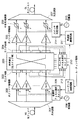
図1は、本発明に係わる光伝送装置の構成を示す機能ブロック図である。この光伝送装置においては、伝送情報を含むチャネル光が装置内をトランスペアレントに伝達される。伝送情報のフォーマットには、例えばSDH(Synchronous Digital Hierarchy)フレームまたはSONET(Synchronous Optical Network)フレームなどの時分割多重形式が適用される。
【0015】
図1において、光ファイバWLを介して到達した波長多重光は、光分波器201によりそれぞれ異なる波長のチャネル光に分波される。各チャネル光はそれぞれ光ファイバ増幅器202を介して光スイッチなどの光学部品200に入射される。光ファイバ増幅器202は、隣接する他の光伝送装置や光中継器との間の光伝送路、あるいは光分波器101などで生じる光損失を、各チャネル光ごとに補償する。
【0016】
光学部品200は、外部から与えられるルーティング情報に基づき、各チャネル光を光のままルーティングする。ここで経路切替されたチャネル光は、光学部品200からそれぞれ光ファイバ増幅器205を介して光合波器207に入射され、波長多重されて光ファイバELに送出される。
【0017】
ところで、各光ファイバ増幅器202には、周波数(ID:identification)発生源208で発生される各チャネル光ごとの固有の変調周波数fが、変調側チャネル選択スイッチ209を介して与えられる。各光ファイバ増幅器202は、与えられる変調周波数fに応じてチャネル光を強度変調し、これにより各チャネル光には、識別可能な固有の変調特性が付加される。
【0018】
変調側チャネル選択スイッチ209は、ルーティング情報に基づくシーケンス制御回路212の制御により動作し、ルーティング情報に則した変調周波数fを光ファイバ増幅器202に切り替え出力する。これにより各チャネル光に付すべき識別特性が、光学部品200のルーティング設定に応じて切り替えられる。
【0019】
光学部品200における入方路および出方路には、各チャネル光ごとにモニタ回路203,204が設けられる。モニタ回路203,204は各チャネル光に付与された変調周波数を読み取り、その結果をモニタ側チャネル選択スイッチ210に与える。モニタ側チャネル選択スイッチ210は、シーケンス制御回路212から与えられる制御信号に応じて切替動作し、ルーティング情報に応じた入出力経路の組み合わせで、各モニタ回路203,204の出力を周波数識別回路211に与える。
【0020】
周波数識別回路211は、モニタ回路203,204で取得された変調周波数fを識別し、その結果をスイッチ判定回路214に与える。スイッチ判定回路214は、識別された変調周波数fをルーティング情報と照合し、光学部品200における誤接続を各チャネル光ごとに判定する。
【0021】
光学部品200から出力される波長光は、装置内誤接続の有無に拘わらず光ファイバ増幅器205に入射される。光ファイバ増幅器205はALC(自動レベル一定制御)駆動され、光学部品200から出力された各チャネル光をレベル補償するとともにその強度変調成分を除去する。その後各チャネル光は可変光減衰器206を介して光合波器207に入射され、波長多重されて光ファイバELに送出される。
【0022】
各可変光減衰器206には、入射されるチャネル光が装置内誤接続を生じたものである場合に、スイッチ判定回路214を介して発振器215からの周波数信号Fが駆動信号として与えられる。可変光減衰器206の減衰率は周波数信号Fに応じて可変され、これにより、誤接続の生じたチャネル光に周波数信号Fに応じた強度変調がかけられる。
【0023】
この強度変調の周波数、すなわち周波数信号Fの周波数は、希土類元素ドープ光ファイバの反転分布の応答周波数の程度とするのが好ましい。このようにすると、装置の後段にALC駆動光ファイバ増幅器などが接続される場合でも、強度変調成分が失われないようにできる。また、併せて強度変調の強度を、後段のALC駆動光ファイバ増幅器により強度変調成分が失われない程度に大きくするとさらに好ましい。
【0024】
このように本実施形態では、各チャネル光を固有の変調周波数fで予め個別に光ファイバ増幅器202で強度変調する。そして、各チャネル光の変調周波数をモニタ回路203,204で読み取り、その結果を周波数識別回路211に与えて各チャネル光を識別する。これをもとに光学部品200のルーティング情報との照合により誤接続の生じたチャネル光を判別する。誤接続と判定されたチャネル光には可変光減衰器206でさらに強度変調をかけ、宛先への情報伝達を抑止するようにしている。
【0025】
このように、誤接続の生じたチャネル光に変調周波数Fで再度強度変調をかけるようにしたので、チャネル光が含む伝送情報が破壊され、従ってチャネル光が誤った宛先に届いたとしても伝送情報の伝達を阻止できる。従ってミスコネクションを防止することが可能になる。また、変調周波数Fを誤接続標識情報として用いることができるので、後段に接続される装置に誤接続が生じたことを伝達することができ、システム保守に役立てることができる。また、強度変調により伝送情報を破壊するようにしているので、光信号自体はそのまま伝達される。これにより後段に接続される光増幅器(中継器)を始めとする、様々な装置やシステムへの動作影響を最小限にできる。
【0026】
また、変調周波数Fを希土類元素ドープ光ファイバの反転分布の応答周波数の程度とするか、あるいは再度の強度変調の強度を、後段のALC駆動光ファイバ増幅器により強度変調成分が失われない程度に大きくすると、装置の後段にALC駆動光ファイバ増幅器などが接続される場合でも、強度変調成分が失われず、より確実にミスコネクションを防止できる。
【0027】
なお、本発明は上記実施の形態に限定されるものではない。例えば図1の可変光減衰器206に代えて、変調周波数Fに応じて利得を制御される光増幅器を設けても良い。もちろん、可変光変調器や高速な光スイッチ素子を設けても同様の効果を得られる。また図1の光ファイバ増幅器205に変調周波数Fを与えて利得制御するようにすれば、構成をより簡易なものとできる。
【0028】
また上記実施形態では、周波数信号Fの周波数を希土類元素ドープ光ファイバの反転分布の応答周波数の程度とするのが好ましいが、必ずしもそうしなくとも良い。例えば、周波数信号Fの周波数を、誤接続チャネル光の波長を波長多重システムに属さない波長に変換できるようなレベルに設定しても良い。
【0029】
また本実施形態では光伝送装置の出力側で誤接続チャネル光に強度変調をかけ、伝送情報の可読性を抑圧するようにしたが、より直接的に、誤接続チャネル光を遮断するようにしても良い。このようにするには、図1の可変光減衰器206に代えて光スイッチを設け、誤接続チャネル光の経路を情報伝送経路から排除する方路へと切り替えるようにすると良い。または光遮断器を設けても同様の効果を得られる。さらに、誤接続チャネル光が入射される光ファイバ増幅器205をオフするようにすれば、より簡易にチャネル光を遮断できる。このほか、本発明の要旨を逸脱しない範囲で種々の変形実施を行うことができる。
【0030】
【発明の効果】
以上詳しく述べたように本発明によれば、装置内誤接続が生じた場合にミスコネクションを防止し得る光伝送装置を提供することができる。
【図面の簡単な説明】
【図1】 本発明に係わる光伝送装置の構成を示す機能ブロック図。
【符号の説明】
WL…光ファイバ
EL…光ファイバ
101…光分波器
200…光学部品
201…光分波器
202…光ファイバ増幅器
203,204…モニタ回路
205…光ファイバ増幅器
206…可変光減衰器
207…光合波器
208…周波数発生源
209…変調側チャネル選択スイッチ
210…モニタ側チャネル選択スイッチ
211…周波数識別回路
212…シーケンス制御回路
214…スイッチ判定回路
215…発振器[0001]
BACKGROUND OF THE INVENTION
The present invention relates to an optical transmission apparatus that is used in a wavelength division multiplexing transmission system or the like, in which channel light is transmitted transparently inside the apparatus, and an erroneous transmission prevention method used in the optical transmission apparatus.
[0002]
[Prior art]
In recent years, communication demand has increased remarkably. In response to this, thickening of the optical backbone communication network has been promoted by DWDM (Dense Wavelength Division Multiplex) technology or the like, but the bottleneck of the optical transmission apparatus has become increasingly prominent. This is because a conventional optical transmission device converts an optical signal having a wavelength corresponding to each channel (hereinafter referred to as channel light) into an electrical signal within the device, and performs routing processing using the electrical signal.
[0003]
Against this background, an all-optical transmission device that does not perform optical-electrical-optical conversion (OEO conversion) inside the device and routes channel light as light is about to be put into practical use. Since all optical transmission equipment does not perform OEO conversion inside the equipment, it is expected that a protocol-free and bit-rate-free optical network can be constructed. Examples of this type of device include an OADM (Optical Add Drop Multiplexer) device and an optical cross connect (Optical Cross Connect) device.
[0004]
This type of apparatus includes various optical units such as an optical switch for switching the channel light path and an optical amplifier for amplifying the channel light. In order to keep these units in a healthy state, it is necessary to reliably detect any failure, erroneous connection that may occur artificially, or erroneous connection due to a software defect. However, since this type of apparatus does not perform OEO conversion, individual channel lights cannot be distinguished from each other by using overhead information of transmission signals.
[0005]
Therefore, various attempts have been made to make it possible to uniquely identify each channel light in the all-optical transmission apparatus. For example, a technique is conceived in which intensity modulation is performed on each channel light with a different pattern and each channel light is identified by reading the modulation pattern. According to such a method, even when all channel lights are transmitted at the same wavelength in the apparatus, it is possible to trace individual channel lights.
[0006]
However, in the current apparatus, each channel light can be uniquely identified, and a technique for subsequent processing has not been established. That is, even if it can be detected that the channel light is connected to the wrong path inside the apparatus, the channel light is connected to the wrong path outside the apparatus and the transmission information is transmitted to the wrong path. There is nothing to prevent a connection (misconnection).
[0007]
The following technologies are disclosed in Patent Documents 1 and 2 below.
In Patent Document 1, in an optical amplifying apparatus that superimposes a monitoring information optical signal on an output optical signal and transfers it downstream, the pumping light power is modulated with the monitoring information, and the gain of the optical amplifier is modulated accordingly. A technique for widening a band given to an information signal is disclosed.
[0008]
Patent Document 2 discloses a technology that enables information transmission using excitation light by modulating excitation light with a high-frequency modulation signal having a period shorter than the fluorescence lifetime in the excited state.
[0009]
[Patent Document 1]
JP-A-7-131421 (paragraph number [0016] etc.)
[0010]
[Patent Document 2]
JP-A-8-331058 (paragraph numbers [0016] to [0023], etc.)
[0011]
[Problems to be solved by the invention]
As described above, even if each channel light can be uniquely identified in the all-optical transmission apparatus, a technique that can prevent misconnection is not yet known. The present invention has been made in view of the above circumstances, and an object of the present invention is to provide an optical transmission apparatus that can prevent misconnection when an in-device misconnection occurs.
[0012]
[Means for Solving the Problems]
In order to achieve the above object, the present invention provides an optical component (for example, an optical switch) that routes a plurality of channel lights each including transmission information as light based on given routing information, and a plurality of channel lights, respectively. A characteristic adding means (for example, an optical fiber amplifier 202 ) for adding a unique identification characteristic before entering the optical component, and each channel light emitted from the optical component is individually identified by monitoring the identification characteristic. An identification unit (for example, a monitor circuit), a determination unit (for example, a switch determination circuit) for comparing each result of identification by the identification unit with the routing information and determining an erroneous connection in the optical component for each channel, and this determination Suppression means for suppressing transmission of the transmission information by channel light determined to be erroneous connection by the means (for example, variable optical reduction An optical attenuator) and an optical fiber amplifier (for example, optical fiber amplifier 205) that is connected to the subsequent stage of the suppression means and that amplifies each channel light by introducing each channel light into an amplifying fiber to which the pump light is optically coupled. And the characteristic adding means modulates the plurality of channel lights with respective unique modulation characteristics to add the identification characteristics, and the suppression means modulates the response frequency of the inversion distribution of the amplification fiber. Modulation means for intensity-modulating the channel light determined to be erroneously connected at a frequency is provided .
[0013]
By taking such means, a characteristic characteristic is added to each channel light by the characteristic adding means, and each channel light is identified by the identifying means based on this. If the identification result and the routing information do not match, an in-device erroneous connection has occurred, and this is determined by the determining means. Information transmission using channel light determined to be erroneously connected is suppressed by blocking means, for example, by blocking light or applying strong intensity modulation. As a result, if an in-device misconnection occurs, even if the channel light reaches the wrong destination, the transmission information has already been destroyed, or the transmission information does not reach the wrong destination. Transmission to the wrong destination is suppressed. Therefore, it is possible to prevent misconnection.
[0014]
DETAILED DESCRIPTION OF THE INVENTION
Hereinafter, embodiments of the present invention will be described in detail with reference to the drawings.
FIG. 1 is a functional block diagram showing a configuration of an optical transmission apparatus according to the present invention. In this optical transmission device, channel light including transmission information is transmitted transparently in the device. As the format of the transmission information, for example, a time division multiplexing format such as an SDH (Synchronous Digital Hierarchy) frame or a SONET (Synchronous Optical Network) frame is applied.
[0015]
In FIG. 1, the wavelength multiplexed light that has arrived through the optical fiber WL is demultiplexed into channel lights having different wavelengths by the
[0016]
The
[0017]
By the way, each
[0018]
The modulation side
[0019]
[0020]
The
[0021]
The wavelength light output from the
[0022]
Each variable
[0023]
The frequency of this intensity modulation, that is, the frequency of the frequency signal F is preferably set to the extent of the response frequency of the inversion distribution of the rare earth element-doped optical fiber. In this way, even when an ALC drive optical fiber amplifier or the like is connected to the subsequent stage of the apparatus, it is possible to prevent the intensity modulation component from being lost. In addition, it is further preferable that the intensity of the intensity modulation is increased to such an extent that the intensity modulation component is not lost by the subsequent ALC drive optical fiber amplifier.
[0024]
As described above, in this embodiment, the intensity of each channel light is individually modulated in advance by the
[0025]
As described above, since the channel light in which the erroneous connection has occurred is subjected to the intensity modulation again at the modulation frequency F, the transmission information included in the channel light is destroyed, and therefore the transmission information is transmitted even if the channel light reaches the wrong destination. Can be prevented. Therefore, it is possible to prevent misconnection. In addition, since the modulation frequency F can be used as erroneous connection indicator information, it can be transmitted that an erroneous connection has occurred in a device connected at a later stage, which can be used for system maintenance. Further, since the transmission information is destroyed by intensity modulation, the optical signal itself is transmitted as it is. As a result, it is possible to minimize the influence of operations on various devices and systems including an optical amplifier (repeater) connected to the subsequent stage.
[0026]
Further, the modulation frequency F is set to the level of the response frequency of the inversion distribution of the rare earth element-doped optical fiber, or the intensity of the intensity modulation again is increased to such an extent that the intensity modulation component is not lost by the subsequent ALC drive optical fiber amplifier. Then, even when an ALC drive optical fiber amplifier or the like is connected to the subsequent stage of the apparatus, the intensity modulation component is not lost, and misconnection can be prevented more reliably.
[0027]
The present invention is not limited to the above embodiment. For example, instead of the variable
[0028]
In the above-described embodiment, the frequency of the frequency signal F is preferably set to the response frequency of the inversion distribution of the rare earth element-doped optical fiber, but this is not necessarily required. For example, the frequency of the frequency signal F may be set to a level at which the wavelength of the misconnected channel light can be converted into a wavelength that does not belong to the wavelength multiplexing system.
[0029]
In the present embodiment, the intensity of the misconnection channel light is modulated on the output side of the optical transmission device to suppress the readability of the transmission information. However, the misconnection channel light may be blocked more directly. good. In order to do this, an optical switch may be provided in place of the variable
[0030]
【The invention's effect】
As described above in detail, according to the present invention, it is possible to provide an optical transmission apparatus capable of preventing misconnection when an in-device misconnection occurs.
[Brief description of the drawings]
FIG. 1 is a functional block diagram showing a configuration of an optical transmission apparatus according to the present invention.
[Explanation of symbols]
WL ... Optical fiber EL ... Optical fiber 101 ...
Claims (6)
前記複数のチャネル光にそれぞれ固有の識別特性を前記光学部品への入射前に付加する特性付加手段と、
前記光学部品から出射される各チャネル光をその前記識別特性をモニタして個別に識別する識別手段と、
この識別手段による識別の結果を前記ルーティング情報と照合して、前記光学部品における誤接続を各チャネルごとに判定する判定手段と、
この判定手段により誤接続と判定されたチャネル光による前記伝送情報の伝送を抑止する抑止手段と、
この抑止手段の後段に接続され、励起光が光結合される増幅用ファイバに各チャネル光が導入され各チャネル光をそれぞれ増幅する光ファイバ増幅器とを具備し、
前記特性付加手段は、前記複数のチャネル光をそれぞれ固有の変調特性で変調して前記識別特性を付加し、
前記抑止手段は、前記増幅用ファイバの反転分布の応答周波数に相当する変調周波数で前記誤接続と判定されたチャネル光を強度変調する変調手段を備えることを特徴とする光伝送装置。An optical component that routes a plurality of channel lights each including transmission information as light based on given routing information;
Characteristic adding means for adding identification characteristics unique to each of the plurality of channel lights before entering the optical component;
Identification means for individually identifying each channel light emitted from the optical component by monitoring the identification characteristics;
A determination unit that compares the result of identification by the identification unit with the routing information and determines an erroneous connection in the optical component for each channel;
Suppression means for suppressing transmission of the transmission information by channel light determined to be erroneous connection by the determination means;
An optical fiber amplifier connected to the subsequent stage of the suppression means, each channel light being introduced into an amplification fiber to which the pump light is optically coupled, and each channel light being amplified;
The characteristic adding means adds the identification characteristic by modulating the plurality of channel lights with respective unique modulation characteristics,
The optical transmission apparatus , wherein the suppression means includes modulation means for intensity-modulating the channel light determined to be erroneously connected at a modulation frequency corresponding to a response frequency of the inversion distribution of the amplification fiber .
Priority Applications (1)
| Application Number | Priority Date | Filing Date | Title |
|---|---|---|---|
| JP2003101713A JP4071663B2 (en) | 2003-04-04 | 2003-04-04 | Optical transmission equipment |
Applications Claiming Priority (1)
| Application Number | Priority Date | Filing Date | Title |
|---|---|---|---|
| JP2003101713A JP4071663B2 (en) | 2003-04-04 | 2003-04-04 | Optical transmission equipment |
Publications (2)
| Publication Number | Publication Date |
|---|---|
| JP2004312256A JP2004312256A (en) | 2004-11-04 |
| JP4071663B2 true JP4071663B2 (en) | 2008-04-02 |
Family
ID=33465416
Family Applications (1)
| Application Number | Title | Priority Date | Filing Date |
|---|---|---|---|
| JP2003101713A Expired - Fee Related JP4071663B2 (en) | 2003-04-04 | 2003-04-04 | Optical transmission equipment |
Country Status (1)
| Country | Link |
|---|---|
| JP (1) | JP4071663B2 (en) |
Families Citing this family (2)
| Publication number | Priority date | Publication date | Assignee | Title |
|---|---|---|---|---|
| JP4852308B2 (en) * | 2005-12-27 | 2012-01-11 | 株式会社日立製作所 | Optical cross-connect device |
| WO2011161891A1 (en) * | 2010-06-24 | 2011-12-29 | 三菱電機株式会社 | Optical add-drop multiplexer (oadm) device |
-
2003
- 2003-04-04 JP JP2003101713A patent/JP4071663B2/en not_active Expired - Fee Related
Also Published As
| Publication number | Publication date |
|---|---|
| JP2004312256A (en) | 2004-11-04 |
Similar Documents
| Publication | Publication Date | Title |
|---|---|---|
| US10826601B2 (en) | Optical switch with path continuity monitoring for optical protection switching | |
| CA2343211C (en) | Method and system for detecting loss of signal in wavelength division multiplexed systems | |
| JP3532759B2 (en) | Relay apparatus and transmission level control method for the same in WDM communication system | |
| US6452701B1 (en) | Wavelength division multiplexing communications network supervisory system | |
| JP6005295B2 (en) | Optical signal-to-noise ratio detection method, system and apparatus | |
| US8554070B2 (en) | Optical transmission apparatus and optical attenuation amount control method | |
| US20110200322A1 (en) | Flexible Branching Unit and System Including the Same | |
| AU2227200A (en) | Optical communication system | |
| US11451294B2 (en) | Method and system to prevent false restoration and protection in optical networks with a sliceable light source | |
| JP2012109653A (en) | Wavelength multiplex transmission device | |
| US7254327B1 (en) | Switching status and performance monitoring technology for wavelength selective switch and optical networks | |
| US9391421B2 (en) | Optical amplification apparatus, optical transmission apparatus, and optical transmission system | |
| JP2951985B2 (en) | Supervisory signal transfer device for optical repeaters | |
| JP2910667B2 (en) | Linear repeater optical amplification transmission equipment | |
| JP4071663B2 (en) | Optical transmission equipment | |
| JP2001257646A (en) | Optical amplifier and wavelength multiplex optical communication system provided with the optical amplifier | |
| JP2001197010A (en) | Optical amplifier, node device, and optical communication network system | |
| EP1011217A2 (en) | Optical repeater | |
| JP2004040241A (en) | Optical transmission device and optical signal path connection monitoring method | |
| JP2005229387A (en) | Optical transmission equipment | |
| US20040109686A1 (en) | Architecture for metropolitan dense wavelength division multiplex network with all-optical reference node | |
| JP3745767B2 (en) | Terminal station apparatus and supervisory control method in WDM communication system | |
| JP4029661B2 (en) | Optical multiplexing / demultiplexing method and apparatus | |
| MXPA01002734A (en) | Method and system for detecting loss of signal in wavelength division multiplexed systems |
Legal Events
| Date | Code | Title | Description |
|---|---|---|---|
| A621 | Written request for application examination |
Free format text: JAPANESE INTERMEDIATE CODE: A621 Effective date: 20051207 |
|
| A977 | Report on retrieval |
Free format text: JAPANESE INTERMEDIATE CODE: A971007 Effective date: 20071029 |
|
| A131 | Notification of reasons for refusal |
Free format text: JAPANESE INTERMEDIATE CODE: A131 Effective date: 20071106 |
|
| A521 | Written amendment |
Free format text: JAPANESE INTERMEDIATE CODE: A523 Effective date: 20071212 |
|
| TRDD | Decision of grant or rejection written | ||
| A01 | Written decision to grant a patent or to grant a registration (utility model) |
Free format text: JAPANESE INTERMEDIATE CODE: A01 Effective date: 20080115 |
|
| A61 | First payment of annual fees (during grant procedure) |
Free format text: JAPANESE INTERMEDIATE CODE: A61 Effective date: 20080117 |
|
| FPAY | Renewal fee payment (event date is renewal date of database) |
Free format text: PAYMENT UNTIL: 20110125 Year of fee payment: 3 |
|
| FPAY | Renewal fee payment (event date is renewal date of database) |
Free format text: PAYMENT UNTIL: 20120125 Year of fee payment: 4 |
|
| LAPS | Cancellation because of no payment of annual fees |