JP4071419B2 - Disk array device - Google Patents
Disk array device Download PDFInfo
- Publication number
- JP4071419B2 JP4071419B2 JP2000159553A JP2000159553A JP4071419B2 JP 4071419 B2 JP4071419 B2 JP 4071419B2 JP 2000159553 A JP2000159553 A JP 2000159553A JP 2000159553 A JP2000159553 A JP 2000159553A JP 4071419 B2 JP4071419 B2 JP 4071419B2
- Authority
- JP
- Japan
- Prior art keywords
- power supply
- chassis
- output
- power
- basic
- Prior art date
- Legal status (The legal status is an assumption and is not a legal conclusion. Google has not performed a legal analysis and makes no representation as to the accuracy of the status listed.)
- Expired - Fee Related
Links
Images


Description
【0001】
【発明の属する技術分野】
本発明は、ディスクアレイにおける制御部と内蔵ディスク、電源と上位及び下位との入出力インタフェースを装備した基本筐体と増設を目的とした内蔵ディスクと電源、入出力インタフェースを装備した増設筐体を接続可能なディスクアレイ装置に属する。
【0002】
【従来の技術】
従来は、システムを停止しないことを前提とし、起動及び停止時の筐体間の連動シーケンスを持たせていない。従って、起動及び停止時には筐体ごとに人手による電源スイッチの操作が必要であった。また、UPS(無停電電源装置)を使用したものとして特開平10-98839「無停電電源装置およびその連動運転方法」に記載されている様に、運転管理装置を用いてUPS、サーバ及びディスクアレイ等を制御するシステムがある。
【0003】
【発明が解決しようとする課題】
前記のようなシステムの場合、装置を停止する際には基本筐体の停止処理ののち、この基本筐体に複数台接続された増設筐体の電源を1台ずつ落とさなければならない。装置を立ち上げる際にも全ての増設筐体の電源をONにした後、基本筐体の電源を立ち上げる必要がある。または電源をそのままとした場合、電源はONのまま、冷却用のFANも回転したままとなり、消費電力及び騒音の点でも好ましくない。また、前記のUPSを用いたシステムに対しても高価なUPSはもちろん、運転管理装置なども用いずに基本筐体に合わせて増設筐体の電源制御を提供する。
【0004】
【課題を解決するための手段】
ディスクアレイの基本筐体及び増設筐体にAC電源を供給するPDB(Power Distribution Box)にAC出力を出力コネクタごとにON/OFFする機能を持たせ、基本筐体からの信号により出力のON/OFFが可能とする。また、PDBはこの基本筐体からの信号を各出力コネクタの横にあるスイッチの切替により隣の出力に送ることが可能であり、1台の基本筐体の信号で隣り合った複数の出力のON/OFFを制御可能である。これにより、基本筐体の動作に対応し増設筐体の電源のON/OFFを可能とする。
【0005】
【発明の実施の形態】
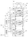
図1のように、本ディスクアレイ装置は基本筐体102と増設筐体Ι103及び増設筐体Π104によって構成される。基本筐体102は、2系の電源109、110と2系入出力インタフェィース105、106と2系の制御部(コントローラ0)107と(コントローラ1)108、これらのコントローラ107、108よりアクセス可能なディスク装置111、112により構成される装置であり、ホスト101と基本筐体102は前述の入出力インタフェース105、106により接続される。基本筐体102には必要に応じて複数台の増設ディスクを搭載した増設筐体103、104を接続することが可能である。基本筐体102のコントローラ107、108と増設筐体103、104内の各ディスク装置119、120との間のインタフェース118、121は、一般のSCSI、ファイバーチャネルなどのインタフェースであり、電源制御などの特別な機能は持たない。
【0006】
ここで本実施例では、基本筐体102、増設筐体103、104ともに独立した2系統の電源109、110、114、115をそれぞれ持っており、それぞれを電源供給装置1系122、2系124に接続している。1系、2系の電源122、124は2重化電源であり、それぞれの筐体内で1台が故障してももう
1台のみで動作が可能である。基本筐体102は電源制御部113を有し、基本筐体102内の電源109、110、コントローラ107、108、ディスク装置111、112の電源を制御可能である。
【0007】
基本筐体102は電源109、110のスイッチONにて、まず電源制御部113のみに電力が供給され、さらにこの電源制御部113がもつスイッチがONされることにより、電源制御部113はコントローラ106、107及びディスク装置111、112に電力を供給する。また、電源109、110OFF時には、まず電源制御部113のスイッチがOFFされることにより、電源制御部113は各コントローラ106、107に対し停止処理を開始するよう信号を送出する。これにより各コントローラ106、107は停止処理を実行し、これが終了すると停止処理が終了したことを電源制御部113に知らせる。電源制御部113は両方のコントローラ106、107から停止処理終了の信号を受信した後、各コントローラ106、107及びディスク装置111、112に対する電力供給を停止する。これに対し増設筐体103、104では電源制御部を持たず、各電源114、115が持つスイッチのONにてディスク装置119、120に電力が供給される。本システムにおける基本筐体102の電源制御部113は、自身が持つスイッチのON及び各コントローラ106、107の停止処理が終了したことを外部の電源供給装置122、124に対し、電源供給の開始及び停止信号として出力する機能を有し、これらの信号は専用連動ケーブル116、117により、電源供給装置122、124に送られる。
【0008】
図2に電源供給装置122、124の内部構成を示す。本装置は電源コネクタ210から入力された電源を、メインブレーカ206を介して、5個の出力209に分配している物であり、各出力209はリレー208により出力のON/OFFがコントロール可能である。基本筐体102との連動ケーブル116、117は電源供給装置122、124のコネクタ202−4に接続される。この信号はリレーコントロール回路205−4に入力される。また、コネクタ202−4に連動ケーブル116、117が接続されたことは信号ラインによりローカル/リモート検出回路204−4に伝達され、リレーコントロール回路205−4をリモートモードにする。出力コネクタ209−4には前述の連動ケーブル116、117で接続された基本筐体102と接続される増設筐体103、104の電源114、115が接続されている。リモートモードに設定されたリレーコントロール回路205−4は基本筐体102からの信号により、AC電源をON/OFF可能なリレー208−4を制御し、増設筐体103、104の電源114、115をON/OFFさせる。ローカルモードの場合、基本筐体からの信号は無視される。
【0009】
コネクタ202−4に基本筐体102からの連動ケーブル116、117が接続されている時、スイッチ203−3をリモートに設定すると、スイッチ203−3がONとなり、基本筐体102からの信号がリレーコントロール回路205−3にも送信される。スイッチ203−3がONになったことは、ローカル/リモート検出回路204−3に伝えられ、ローカル/リモート検出回路204−3は、リレーコントロール回路205−3をリモートモードに設定する。これにより、1台の基本筐体から複数台の増設筐体の電源ON/OFFをコントロールできる。
【0010】
コネクタ207は基本筐体102からの制御信号の出力であり、本電源供給装置122、124が受信した信号を出力可能であり、ここから他の電源供給装置の入力、例えばコネクタ202−5に接続することにより、この出力である出力209−5を連動させることが可能である。これにより本図のように電源供給装置122、124が出力209を5個しか持たない場合でも5台以上の増設筐体103、104の連動を可能にする。
【0011】
図3にローカル/リモート検出回路204−4、リレーコントロール回路205−4の概略論理図を示す。ローカル/リモート検出回路204−4は基本筐体102との連動ケーブル116、117が接続されているか又は連動スイッチがONになっている時リレーコントロール回路205−4にリモートON信号を送出する。リレーコントロール回路205−4はリモートON信号が入力されている時、入力される出力ON/OFF信号に従いリレー208をコントロールする。時間監視回路306は、リレー208ON時の突入電流を低減するものであり、メインブレーカ206のON時または出力ON信号入力時にすべてのリレー208が同時にONとならないようにしている。
【0012】
図4に電源オフ時の制御フローを示す。基本筐体102の電源をオフし(402)、停止処理開始後(403)、キャッシュ書き込み処理を実施し(404)、増設筐体103、104の電源をON状態にした(408)ドライブに基本筐体102のキャッシュの内容を書き込む(409)。これは、キャッシュは揮発メモリを使用しているため、電源オフ後は内容が消えてしまうことを防ぐため実施される。基本筐体102が停止処理終了後(405)、AC供給されている(412)電源供給装置122、124に停止信号を送信する。電源供給装置122、124は停止処理終了を認識すると(413)、増設筐体103、104のAC供給の切断を行う( 414 )。
【0013】
基本筐体102は、電源供給装置122、124が増設筐体103、104のAC供給を停止すると同時に、バッテリスイッチを除く部分の電源109、110をオフとする(406)。
【0014】
図5に電源オン時の制御フローを示す。基本筐体102の電源109、110をオンすると(502)、コントローラ107、108は起動処理を開始する(503)。さらに、電源オンと連動して、電源供給装置122、124に電源オン信号を送信する。電源供給装置122、124は、基本筐体102からの電源オン信号を受信すると(509)、各増設筐体103、104へのAC供給を再開する(510)。各増設筐体103、104は電源をオンとする(507)。ただし、突入電流防止のため1筐体ずつにAC供給を開始する。基本筐体102は、起動処理終了後(504)、増設筐体にアクセスすることができる( 505 )。
【0015】
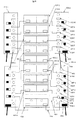
図6に構成例を示す。本構成では、基本筐体1台に増設筐体8台が接続されており、基本筐体602は増設筐体601−1〜601−8の接続されているコネクタ612−2を連動させるコネクタ609と連動ケーブル606で接続されている。スイッチ607−2〜607−4はリモート側に設定されており、出力612−3〜612−5は出力612−2とともに基本筐体602と連動して制御される。出力コネクタ610はもう一台の電源供給装置603−2の入力コネクタ611と接続され、出力612−6を連動させている。スイッチ607−5〜607−7はリモート側に設定されており、1台の基本筐体602で計8台の増設筐体601−1〜601−8と電源連動をしている。スイッチ607−8はローカル側に設定されており、出力612−10は連動しない。
【0016】
【発明の効果】
基本筐体と増設筐体は、電源供給装置を設けることで、基本筐体の電源監視/制御モニタ内スイッチをオン/オフする事で、各筐体電源スイッチをオン/オフする事なく、計画停止及び立ち上げを実施できる。また、増設筐体の未使用時に増設筐体への電力供給を遮断することにより、無駄な消費電力の節約、冷却FANの停止による騒音の低減などが期待できる。
【0017】
また、電源供給装置を設けることで、内部スイッチと連動ケーブルにより、筐体へのAC供給をどの筐体まで連動するかを選択することができる。さらに、任意のポートにて接続可能であるため、に接続することで、使用可能となる。そして、増設筐体の追加により、既存のコンセントが不足した場合、電源供給装置間をケーブルで接続することにより、連動コンセントの増設が容易であり、増設する筐体の台数に制限を受けない。
【図面の簡単な説明】
【図1】 本発明のシステム構成詳細図である。
【図2】 電源供給装置の構成詳細図である。
【図3】 電源供給装置の概略論理図である。
【図4】 電源オフ時の制御フローである。
【図5】 電源オン時の制御フローである。
【図6】 システム構成例である。
【符号の説明】
101‥‥ホスト
102‥‥基本筐体
103‥‥増設筐体Ι
104‥‥増設筐体Π
105、106‥‥ホストインタフェース
107、108‥‥コントローラ
109‥‥基本筐体用電源1系
110‥‥基本筐体用電源2系
111、112‥‥ディスク装置
113‥‥電源制御部
114‥‥増設筐体用電源1系
115‥‥増設筐体用電源2系
116、117‥‥連動ケーブル
118‥‥ディスクインタフェース
119、120‥‥ディスク装置
121‥‥ディスクインタフェース
122‥‥電源供給装置1系
123‥‥電源ケーブル
124‥‥電源供給装置2系
202−1〜202−5‥‥連動信号入力コネクタ
203−1〜203−4‥‥連動接続スイッチ
204−1〜204−5‥‥ローカル/リモート検出回路
205−1〜205−5‥‥リレーコントロール回路
206‥‥メインブレーカ
207‥‥連動信号出力コネクタ
208−1〜208−5‥‥リレー
209−1〜209−5‥‥出力コンセント
210‥‥電源コネクタ
301‥‥ケーブル接続条件
303、309‥‥OR回路
304‥‥リモート信号ON
306‥‥時間監視回路
307、308‥‥AND回路
402‥‥電源スイッチオフ
403‥‥停止処理開始
404‥‥キャッシュ書き込み処理
405‥‥停止処理終了
406‥‥電源オフ
407‥‥増設筐体の制御フロー
408‥‥電源オン状態
409‥‥ドライブ書き込み処理
410‥‥電源オフ
412‥‥AC供給
413‥‥停止処理終了を認識
414‥‥増設筐体へのAC供給を切断
502‥‥電源スイッチオン
503‥‥起動処理開始
504‥‥起動処理終了
505‥‥増設筐体にアクセス
507−1〜507−4‥‥電源オン
509‥‥電源オン信号受理
510−1〜510−4‥‥増設筐体にACを供給
601−1〜601−8‥‥増設筐体
602‥‥基本筐体
603−1〜603−4‥‥電源供給装置
604‥‥AC電源
605‥‥電源ケーブル
606‥‥基本筐体連動ケーブル
607−1〜607−8‥‥連動切り替えスイッチ
608‥‥接続ケーブル
609‥‥連動入力コネクタ
610‥‥連動出力コネクタ
611‥‥連動入力コネクタ
612−1〜612−10‥‥電源出力コネクタ[0001]
BACKGROUND OF THE INVENTION
The present invention is equipped with the control unit internal disk, power supply and the upper and internal disk and power supply to the base enclosure and expansion equipped with input and output in tough Esu with the lower purposes, the input and output in tough Esu in the disk array It belongs to a disk array device to which an additional chassis can be connected.
[0002]
[Prior art]
Conventionally, on the premise that the system is not stopped, there is no interlocking sequence between cases at the time of starting and stopping. Therefore, it is necessary to manually operate the power switch for each case when starting and stopping. Further, as described in Japanese Patent Laid-Open No. 10-98839 “Uninterruptible Power Supply and its Interlocking Operation Method” as using UPS (Uninterruptible Power Supply), UPS, server and disk array using operation management device There is a system that controls etc.
[0003]
[Problems to be solved by the invention]
In the case of the system as described above, when stopping the apparatus, after the stop process of the basic chassis, the power of the additional chassis connected to the basic chassis must be turned off one by one. When starting up the apparatus, it is necessary to turn on the power supply of the basic enclosure after turning on the power supply of all the additional enclosures. Alternatively, when the power source is left as it is, the power source is kept on and the cooling FAN is also rotated, which is not preferable in terms of power consumption and noise. Further, not only an expensive UPS but also an operation management device or the like is used for a system using the UPS, and power supply control of an additional chassis is provided in accordance with the basic chassis.
[0004]
[Means for Solving the Problems]
A PDB (Power Distribution Box) that supplies AC power to the basic chassis and additional chassis of the disk array has a function to turn on / off the AC output for each output connector, and the output is turned on / off by a signal from the basic chassis. It can be turned off. In addition, the PDB can send a signal from this basic housing to the adjacent output by switching a switch beside each output connector, and a plurality of adjacent outputs can be output by a signal from one basic housing. ON / OFF can be controlled. As a result, the power supply of the additional chassis can be turned on / off corresponding to the operation of the basic chassis.
[0005]
DETAILED DESCRIPTION OF THE INVENTION
As in FIG. 1, the disk array device is configured with
[0006]
Here, in this embodiment, the
Operation with only one unit is possible. The
[0007]
In the
[0008]
FIG. 2 shows the internal configuration of the
[0009]
When the
[0010]
The
[0011]
FIG. 3 shows a schematic logic diagram of the local / remote detection circuit 204-4 and the relay control circuit 205-4 . The local / remote detection circuit 204-4 sends a remote ON signal to the relay control circuit 205-4 when the
[0012]
FIG. 4 shows a control flow when the power is turned off. The
[0013]
The
[0014]
FIG. 5 shows a control flow when the power is turned on. When the power supplies 109 and 110 of the
[0015]
FIG. 6 shows a configuration example. In this configuration, and additional enclosure eight to one basic enclosure is connected, the
[0016]
【The invention's effect】
Basic chassis and additional chassis can be planned without turning on / off each chassis power switch by turning on / off the power monitoring / control monitor switch of the basic chassis by providing a power supply device. You can stop and start up. In addition, by cutting off the power supply to the expansion enclosure when the expansion enclosure is not in use, it can be expected to save unnecessary power consumption and to reduce noise by stopping the cooling FAN.
[0017]
In addition, by providing the power supply device, it is possible to select up to which case the AC supply to the case is interlocked by the internal switch and the interlocking cable. Furthermore, since it can be connected at an arbitrary port, it can be used by connecting to. When existing outlets are insufficient due to the addition of additional enclosures, it is easy to add linked outlets by connecting the power supply devices with cables, and the number of enclosures to be added is not limited.
[Brief description of the drawings]
FIG. 1 is a detailed system configuration diagram of the present invention .
FIG. 2 is a detailed configuration diagram of a power supply device .
FIG. 3 is a schematic logic diagram of a power supply device .
FIG. 4 is a control flow when power is turned off .
FIG. 5 is a control flow at power-on .
FIG. 6 is a system configuration example .
[Explanation of symbols]
101 ... Host 102 ...
104 ... Additional chassis
105, 106 ...
306 ...
Claims (3)
前記電源供給装置は、主電源と前記基本筐体及び前記複数の増設筐体との間に各筐体から独立して配置されて、前記基本筐体からの開始及び停止を指令する1つの出力オンオフ信号によって前記主電源からの電源を各筐体に供給し、各増設筐体への基本筐体と連動した電源供給の有無が各筐体への各電源出力毎に当該電源供給装置に設けられたスイッチによって設定されるものであり、
前記基本筐体は、前記出力オンオフ信号を前記電源供給装置に送る電源制御部を有し、
更に前記電源供給装置は、各筐体に各電源出力を供給する複数の出力系統を有し、各出力系統は、前記出力オンオフ信号を受け得る信号入力端子と、前記基本筐体と前記増設筐体との連動の有無を設定する連動切替スイッチと、前記主電源と電源出力端間に配置される中継スイッチと、前記出力オンオフ信号と前記連動切替スイッチの出力とに基づいて前記中継スイッチを制御する中継制御部と、を含み、
前記複数の出力系統を間に挟む両側の各出力系統の2つの信号入力端子間に前記各出力系統の連動切替スイッチの開閉回路が直列に接続され、該連動切替スイッチ相互の各接続点がそれぞれ各出力系統の信号入力端子に接続され、
前記電源制御部から前記電源供給装置のいずれかの出力系統の信号入力端子に前記出力オンオフ信号が供給されることにより、出力オンオフ信号が供給された出力系統と前記連動切替スイッチにより連動設定された出力系統とが各々の出力系統の前記中継スイッチを導通させる、ディスクアレイ装置。 A disk array device comprising: a basic chassis having a controller and a disk device; a plurality of additional chassis having an additional disk device; and a power supply device for supplying power to the basic chassis and the plurality of additional chassis. There,
The power supply device is arranged between a main power source, the basic casing, and the plurality of additional casings independently from each casing, and outputs one command for starting and stopping from the basic casing The power supply from the main power supply is supplied to each chassis by an on / off signal, and whether or not power is supplied in conjunction with the basic chassis to each additional chassis is provided for each power output to each chassis. Set by the switch
The basic casing has a power control unit that sends the output on / off signal to the power supply device,
Further, the power supply device has a plurality of output systems for supplying each power output to each housing, and each output system has a signal input terminal that can receive the output on / off signal, the basic housing, and the additional housing. Control of the relay switch based on an interlocking switch for setting presence / absence of interlocking with the body, a relay switch arranged between the main power source and the power output terminal, the output on / off signal and the output of the interlocking switch Including a relay control unit,
The open / close circuit of the interlocking switch of each output system is connected in series between two signal input terminals of each output system on both sides of the plurality of output systems, and each connection point between the interlocking switches is respectively Connected to the signal input terminal of each output system,
When the output on / off signal is supplied from the power control unit to the signal input terminal of any output system of the power supply device, the output system to which the output on / off signal is supplied and the interlock changeover switch are set in conjunction with each other. A disk array device in which an output system conducts the relay switch of each output system.
前記電源供給装置は、主電源と前記基本筐体及び前記複数の増設筐体との間に各筐体から独立して配置されて、前記基本筐体からの開始及び停止を指令する1つの出力オンオフ信号によって前記主電源からの電源を各筐体に供給し、各増設筐体への基本筐体と連動した電源供給の有無が各筐体への各電源出力毎に当該電源供給装置に設けられたスイッチによって設定されるものであり、
前記電源供給装置は複数台備えられ、各電源供給装置は前記基本筐体から受信した出力オンオフ信号を出力する機能を有し、当該出力を他の前記電源供給装置に入力することにより、複数台の前記電源供給装置を連動させ、1台の前記電源供給装置に接続可能な台数を超える前記増設筐体を連動させることを特徴とするディスクアレイ装置。 A disk array device comprising: a basic chassis having a controller and a disk device; a plurality of additional chassis having an additional disk device; and a power supply device for supplying power to the basic chassis and the plurality of additional chassis. There,
The power supply device is arranged between a main power source, the basic casing, and the plurality of additional casings independently from each casing, and outputs one command for starting and stopping from the basic casing The power supply from the main power supply is supplied to each chassis by an on / off signal, and whether or not power is supplied in conjunction with the basic chassis to each additional chassis is provided for each power output to each chassis. Set by the switch
A plurality of the power supply devices are provided, each power supply device has a function of outputting an output on / off signal received from the basic housing, and a plurality of power supply devices are input by inputting the output to the other power supply devices. The disk array apparatus, wherein the power supply apparatuses are interlocked, and the additional enclosures exceeding the number connectable to one power supply apparatus are interlocked.
Priority Applications (1)
| Application Number | Priority Date | Filing Date | Title |
|---|---|---|---|
| JP2000159553A JP4071419B2 (en) | 2000-05-25 | 2000-05-25 | Disk array device |
Applications Claiming Priority (1)
| Application Number | Priority Date | Filing Date | Title |
|---|---|---|---|
| JP2000159553A JP4071419B2 (en) | 2000-05-25 | 2000-05-25 | Disk array device |
Publications (3)
| Publication Number | Publication Date |
|---|---|
| JP2001339853A JP2001339853A (en) | 2001-12-07 |
| JP2001339853A5 JP2001339853A5 (en) | 2006-12-07 |
| JP4071419B2 true JP4071419B2 (en) | 2008-04-02 |
Family
ID=18663856
Family Applications (1)
| Application Number | Title | Priority Date | Filing Date |
|---|---|---|---|
| JP2000159553A Expired - Fee Related JP4071419B2 (en) | 2000-05-25 | 2000-05-25 | Disk array device |
Country Status (1)
| Country | Link |
|---|---|
| JP (1) | JP4071419B2 (en) |
Cited By (1)
| Publication number | Priority date | Publication date | Assignee | Title |
|---|---|---|---|---|
| JP2012120430A (en) * | 2010-11-30 | 2012-06-21 | Ls Industrial Systems Co Ltd | Multi-level inverter having dual controller |
Families Citing this family (15)
| Publication number | Priority date | Publication date | Assignee | Title |
|---|---|---|---|---|
| JP4216006B2 (en) | 2002-06-14 | 2009-01-28 | 株式会社日立製作所 | Storage device control method |
| JP4230189B2 (en) | 2002-10-03 | 2009-02-25 | 株式会社日立製作所 | Disk array device and power supply method thereof |
| JP4025216B2 (en) * | 2003-02-21 | 2007-12-19 | 株式会社日立製作所 | Uninterruptible power system |
| JP4919752B2 (en) | 2006-09-29 | 2012-04-18 | 株式会社日立製作所 | Storage controller |
| JP4749308B2 (en) * | 2006-10-20 | 2011-08-17 | 株式会社日立製作所 | Power supply device and power supply method for power supply device |
| JP5068086B2 (en) * | 2007-02-16 | 2012-11-07 | 株式会社日立製作所 | Storage controller |
| JP2008243148A (en) * | 2007-03-29 | 2008-10-09 | Nec Corp | Disk array device |
| JP2009015584A (en) | 2007-07-04 | 2009-01-22 | Hitachi Ltd | Storage control device and method for controlling power supply of casing unit |
| JP4414452B2 (en) | 2007-08-27 | 2010-02-10 | 富士通株式会社 | Storage device and stop method for stopping additional storage device operating in the storage device |
| JP4982304B2 (en) * | 2007-09-04 | 2012-07-25 | 株式会社日立製作所 | Storage system that understands the occurrence of power failure |
| JP4819088B2 (en) * | 2008-04-25 | 2011-11-16 | 富士通株式会社 | Storage device and method for starting the storage device |
| WO2010055549A1 (en) | 2008-11-17 | 2010-05-20 | Hitachi, Ltd. | Storage control apparatus and storage control method |
| JP4816983B2 (en) | 2008-12-26 | 2011-11-16 | 日本電気株式会社 | Disk array device, power control method and power control program for disk array device |
| JP5251542B2 (en) * | 2009-01-27 | 2013-07-31 | 富士通株式会社 | Power supply design program, method and apparatus |
| CN107783726B (en) | 2016-08-31 | 2019-11-12 | 华为技术有限公司 | The method of signal is transmitted in storage system and storage system |
-
2000
- 2000-05-25 JP JP2000159553A patent/JP4071419B2/en not_active Expired - Fee Related
Cited By (1)
| Publication number | Priority date | Publication date | Assignee | Title |
|---|---|---|---|---|
| JP2012120430A (en) * | 2010-11-30 | 2012-06-21 | Ls Industrial Systems Co Ltd | Multi-level inverter having dual controller |
Also Published As
| Publication number | Publication date |
|---|---|
| JP2001339853A (en) | 2001-12-07 |
Similar Documents
| Publication | Publication Date | Title |
|---|---|---|
| JP4071419B2 (en) | Disk array device | |
| JP2004022058A (en) | Control method of storage device, and storage device | |
| US6744150B2 (en) | Outlet strip controlled by PC using low voltage powertap | |
| US6639329B2 (en) | Isolated power input architecture | |
| TW201320140A (en) | Powre supply system with automatic transfer function and method of controlling the same | |
| JP2000105638A (en) | Usb device and usb connection system | |
| WO2014177056A1 (en) | Low-power consumption standby circuit device, air conditioner and control method for air conditioner | |
| CN100394354C (en) | Power supply for computer system by USB keyboard | |
| CN103166313A (en) | Direct current solid state power controller | |
| JP3171794B2 (en) | Uninterruptible power supply and linked operation method | |
| CN101677475B (en) | Power management method, equipment and mobile terminal thereof | |
| US20040057182A1 (en) | Method and control apparatus for controlling two hot-swapable IDE devices | |
| EP0757321B1 (en) | I/O bus in a multiple drive library computer system | |
| JPH11212682A (en) | Ganged on/off method of local system power supply and power supply control system | |
| CN103532977A (en) | Secure access equipment for intranet and extranet | |
| JP2005033987A (en) | Computer system | |
| CN1301469C (en) | Control circuit and method of double hot plug-in IDE devices | |
| CN1312817C (en) | Current induced switch device | |
| JP2000163164A (en) | Power source controller and no-break power unit | |
| JP3085680U (en) | Switching device for personal computer | |
| WO2021166838A1 (en) | Uninterruptible power supply and uninterruptible power supply system equipped with same | |
| JP2000236587A (en) | Non-power cut power unit and information communication system using the same | |
| CN213659440U (en) | Channel control device and recording and broadcasting equipment comprising same | |
| KR20090022533A (en) | Device and method for providing hot-swap function using switching regulator | |
| CN108429336A (en) | A kind of data center and its method of supplying power to |
Legal Events
| Date | Code | Title | Description |
|---|---|---|---|
| RD01 | Notification of change of attorney |
Free format text: JAPANESE INTERMEDIATE CODE: A7421 Effective date: 20060418 |
|
| A521 | Written amendment |
Free format text: JAPANESE INTERMEDIATE CODE: A821 Effective date: 20061017 Free format text: JAPANESE INTERMEDIATE CODE: A523 Effective date: 20061017 |
|
| A621 | Written request for application examination |
Free format text: JAPANESE INTERMEDIATE CODE: A621 Effective date: 20061017 |
|
| RD02 | Notification of acceptance of power of attorney |
Free format text: JAPANESE INTERMEDIATE CODE: A7422 Effective date: 20061017 |
|
| A977 | Report on retrieval |
Free format text: JAPANESE INTERMEDIATE CODE: A971007 Effective date: 20070704 |
|
| A131 | Notification of reasons for refusal |
Free format text: JAPANESE INTERMEDIATE CODE: A131 Effective date: 20070706 |
|
| RD04 | Notification of resignation of power of attorney |
Free format text: JAPANESE INTERMEDIATE CODE: A7424 Effective date: 20070731 |
|
| A521 | Written amendment |
Free format text: JAPANESE INTERMEDIATE CODE: A523 Effective date: 20070904 |
|
| A02 | Decision of refusal |
Free format text: JAPANESE INTERMEDIATE CODE: A02 Effective date: 20071010 |
|
| A521 | Written amendment |
Free format text: JAPANESE INTERMEDIATE CODE: A523 Effective date: 20071205 |
|
| A911 | Transfer of reconsideration by examiner before appeal (zenchi) |
Free format text: JAPANESE INTERMEDIATE CODE: A911 Effective date: 20071214 |
|
| TRDD | Decision of grant or rejection written | ||
| A01 | Written decision to grant a patent or to grant a registration (utility model) |
Free format text: JAPANESE INTERMEDIATE CODE: A01 Effective date: 20080110 |
|
| A61 | First payment of annual fees (during grant procedure) |
Free format text: JAPANESE INTERMEDIATE CODE: A61 Effective date: 20080117 |
|
| R150 | Certificate of patent or registration of utility model |
Free format text: JAPANESE INTERMEDIATE CODE: R150 |
|
| FPAY | Renewal fee payment (event date is renewal date of database) |
Free format text: PAYMENT UNTIL: 20110125 Year of fee payment: 3 |
|
| FPAY | Renewal fee payment (event date is renewal date of database) |
Free format text: PAYMENT UNTIL: 20110125 Year of fee payment: 3 |
|
| FPAY | Renewal fee payment (event date is renewal date of database) |
Free format text: PAYMENT UNTIL: 20120125 Year of fee payment: 4 |
|
| FPAY | Renewal fee payment (event date is renewal date of database) |
Free format text: PAYMENT UNTIL: 20130125 Year of fee payment: 5 |
|
| LAPS | Cancellation because of no payment of annual fees |