JP4070245B2 - Suspension with biaxial shielded conductor trace array - Google Patents
Suspension with biaxial shielded conductor trace array Download PDFInfo
- Publication number
- JP4070245B2 JP4070245B2 JP53295598A JP53295598A JP4070245B2 JP 4070245 B2 JP4070245 B2 JP 4070245B2 JP 53295598 A JP53295598 A JP 53295598A JP 53295598 A JP53295598 A JP 53295598A JP 4070245 B2 JP4070245 B2 JP 4070245B2
- Authority
- JP
- Japan
- Prior art keywords
- electrical
- load beam
- flexure
- electrical signal
- assembly
- Prior art date
- Legal status (The legal status is an assumption and is not a legal conclusion. Google has not performed a legal analysis and makes no representation as to the accuracy of the status listed.)
- Expired - Lifetime
Links
- 239000004020 conductor Substances 0.000 title claims description 65
- 239000000725 suspension Substances 0.000 title claims description 15
- 238000010292 electrical insulation Methods 0.000 claims description 13
- 238000003860 storage Methods 0.000 claims description 12
- 239000010409 thin film Substances 0.000 claims description 9
- 229910052751 metal Inorganic materials 0.000 claims description 6
- 239000002184 metal Substances 0.000 claims description 6
- 239000003989 dielectric material Substances 0.000 claims description 2
- 238000001465 metallisation Methods 0.000 claims 1
- 239000010410 layer Substances 0.000 description 45
- 238000000034 method Methods 0.000 description 9
- 239000010935 stainless steel Substances 0.000 description 9
- 229910001220 stainless steel Inorganic materials 0.000 description 9
- RYGMFSIKBFXOCR-UHFFFAOYSA-N Copper Chemical compound [Cu] RYGMFSIKBFXOCR-UHFFFAOYSA-N 0.000 description 8
- 229910052802 copper Inorganic materials 0.000 description 8
- 239000010949 copper Substances 0.000 description 8
- 238000013461 design Methods 0.000 description 7
- 239000000463 material Substances 0.000 description 7
- 229920001721 polyimide Polymers 0.000 description 6
- 239000004642 Polyimide Substances 0.000 description 5
- 239000000919 ceramic Substances 0.000 description 5
- 239000000853 adhesive Substances 0.000 description 4
- 230000001070 adhesive effect Effects 0.000 description 4
- 230000008901 benefit Effects 0.000 description 4
- 230000015572 biosynthetic process Effects 0.000 description 3
- 238000000151 deposition Methods 0.000 description 3
- 230000000694 effects Effects 0.000 description 3
- 230000001965 increasing effect Effects 0.000 description 3
- 229920005989 resin Polymers 0.000 description 3
- 239000011347 resin Substances 0.000 description 3
- 229910000881 Cu alloy Inorganic materials 0.000 description 2
- PXHVJJICTQNCMI-UHFFFAOYSA-N Nickel Chemical compound [Ni] PXHVJJICTQNCMI-UHFFFAOYSA-N 0.000 description 2
- 230000000712 assembly Effects 0.000 description 2
- 238000000429 assembly Methods 0.000 description 2
- DMFGNRRURHSENX-UHFFFAOYSA-N beryllium copper Chemical compound [Be].[Cu] DMFGNRRURHSENX-UHFFFAOYSA-N 0.000 description 2
- 230000005540 biological transmission Effects 0.000 description 2
- 239000010408 film Substances 0.000 description 2
- PCHJSUWPFVWCPO-UHFFFAOYSA-N gold Chemical compound [Au] PCHJSUWPFVWCPO-UHFFFAOYSA-N 0.000 description 2
- 229910052737 gold Inorganic materials 0.000 description 2
- 239000010931 gold Substances 0.000 description 2
- 230000001939 inductive effect Effects 0.000 description 2
- 238000005461 lubrication Methods 0.000 description 2
- 238000012986 modification Methods 0.000 description 2
- 230000004048 modification Effects 0.000 description 2
- 239000002952 polymeric resin Substances 0.000 description 2
- 239000000758 substrate Substances 0.000 description 2
- 229920003002 synthetic resin Polymers 0.000 description 2
- 238000012546 transfer Methods 0.000 description 2
- BQCADISMDOOEFD-UHFFFAOYSA-N Silver Chemical compound [Ag] BQCADISMDOOEFD-UHFFFAOYSA-N 0.000 description 1
- 239000012790 adhesive layer Substances 0.000 description 1
- 230000004075 alteration Effects 0.000 description 1
- 238000013459 approach Methods 0.000 description 1
- 238000005253 cladding Methods 0.000 description 1
- 239000011248 coating agent Substances 0.000 description 1
- 238000000576 coating method Methods 0.000 description 1
- 150000001875 compounds Chemical class 0.000 description 1
- 230000001010 compromised effect Effects 0.000 description 1
- 238000013500 data storage Methods 0.000 description 1
- 230000008021 deposition Effects 0.000 description 1
- 238000011161 development Methods 0.000 description 1
- 238000011143 downstream manufacturing Methods 0.000 description 1
- 230000002500 effect on skin Effects 0.000 description 1
- 238000004070 electrodeposition Methods 0.000 description 1
- 238000005516 engineering process Methods 0.000 description 1
- 238000005530 etching Methods 0.000 description 1
- 239000000945 filler Substances 0.000 description 1
- 239000012530 fluid Substances 0.000 description 1
- 238000009413 insulation Methods 0.000 description 1
- 230000010354 integration Effects 0.000 description 1
- 238000010030 laminating Methods 0.000 description 1
- 239000007788 liquid Substances 0.000 description 1
- 230000007774 longterm Effects 0.000 description 1
- 238000004519 manufacturing process Methods 0.000 description 1
- 239000012528 membrane Substances 0.000 description 1
- 229910052759 nickel Inorganic materials 0.000 description 1
- 238000000059 patterning Methods 0.000 description 1
- 230000035699 permeability Effects 0.000 description 1
- 238000000206 photolithography Methods 0.000 description 1
- 238000001020 plasma etching Methods 0.000 description 1
- 238000007747 plating Methods 0.000 description 1
- 230000008569 process Effects 0.000 description 1
- 238000012216 screening Methods 0.000 description 1
- 239000004065 semiconductor Substances 0.000 description 1
- 230000035945 sensitivity Effects 0.000 description 1
- 229910052709 silver Inorganic materials 0.000 description 1
- 239000004332 silver Substances 0.000 description 1
- 238000004528 spin coating Methods 0.000 description 1
- 238000000992 sputter etching Methods 0.000 description 1
- 238000000427 thin-film deposition Methods 0.000 description 1
Images


Classifications
-
- G—PHYSICS
- G11—INFORMATION STORAGE
- G11B—INFORMATION STORAGE BASED ON RELATIVE MOVEMENT BETWEEN RECORD CARRIER AND TRANSDUCER
- G11B5/00—Recording by magnetisation or demagnetisation of a record carrier; Reproducing by magnetic means; Record carriers therefor
- G11B5/48—Disposition or mounting of heads or head supports relative to record carriers ; arrangements of heads, e.g. for scanning the record carrier to increase the relative speed
- G11B5/4806—Disposition or mounting of heads or head supports relative to record carriers ; arrangements of heads, e.g. for scanning the record carrier to increase the relative speed specially adapted for disk drive assemblies, e.g. assembly prior to operation, hard or flexible disk drives
- G11B5/486—Disposition or mounting of heads or head supports relative to record carriers ; arrangements of heads, e.g. for scanning the record carrier to increase the relative speed specially adapted for disk drive assemblies, e.g. assembly prior to operation, hard or flexible disk drives with provision for mounting or arranging electrical conducting means or circuits on or along the arm assembly
-
- G—PHYSICS
- G11—INFORMATION STORAGE
- G11B—INFORMATION STORAGE BASED ON RELATIVE MOVEMENT BETWEEN RECORD CARRIER AND TRANSDUCER
- G11B21/00—Head arrangements not specific to the method of recording or reproducing
- G11B21/16—Supporting the heads; Supporting the sockets for plug-in heads
-
- G—PHYSICS
- G11—INFORMATION STORAGE
- G11B—INFORMATION STORAGE BASED ON RELATIVE MOVEMENT BETWEEN RECORD CARRIER AND TRANSDUCER
- G11B5/00—Recording by magnetisation or demagnetisation of a record carrier; Reproducing by magnetic means; Record carriers therefor
- G11B5/48—Disposition or mounting of heads or head supports relative to record carriers ; arrangements of heads, e.g. for scanning the record carrier to increase the relative speed
- G11B5/4806—Disposition or mounting of heads or head supports relative to record carriers ; arrangements of heads, e.g. for scanning the record carrier to increase the relative speed specially adapted for disk drive assemblies, e.g. assembly prior to operation, hard or flexible disk drives
- G11B5/4846—Constructional details of the electrical connection between arm and support
-
- G—PHYSICS
- G11—INFORMATION STORAGE
- G11B—INFORMATION STORAGE BASED ON RELATIVE MOVEMENT BETWEEN RECORD CARRIER AND TRANSDUCER
- G11B5/00—Recording by magnetisation or demagnetisation of a record carrier; Reproducing by magnetic means; Record carriers therefor
- G11B5/48—Disposition or mounting of heads or head supports relative to record carriers ; arrangements of heads, e.g. for scanning the record carrier to increase the relative speed
- G11B5/4806—Disposition or mounting of heads or head supports relative to record carriers ; arrangements of heads, e.g. for scanning the record carrier to increase the relative speed specially adapted for disk drive assemblies, e.g. assembly prior to operation, hard or flexible disk drives
- G11B5/4853—Constructional details of the electrical connection between head and arm
-
- G—PHYSICS
- G11—INFORMATION STORAGE
- G11B—INFORMATION STORAGE BASED ON RELATIVE MOVEMENT BETWEEN RECORD CARRIER AND TRANSDUCER
- G11B23/00—Record carriers not specific to the method of recording or reproducing; Accessories, e.g. containers, specially adapted for co-operation with the recording or reproducing apparatus ; Intermediate mediums; Apparatus or processes specially adapted for their manufacture
- G11B23/0007—Circuits or methods for reducing noise, for correction of distortion, or for changing density of recorded information
-
- G—PHYSICS
- G11—INFORMATION STORAGE
- G11B—INFORMATION STORAGE BASED ON RELATIVE MOVEMENT BETWEEN RECORD CARRIER AND TRANSDUCER
- G11B5/00—Recording by magnetisation or demagnetisation of a record carrier; Reproducing by magnetic means; Record carriers therefor
- G11B5/127—Structure or manufacture of heads, e.g. inductive
- G11B5/33—Structure or manufacture of flux-sensitive heads, i.e. for reproduction only; Combination of such heads with means for recording or erasing only
- G11B5/39—Structure or manufacture of flux-sensitive heads, i.e. for reproduction only; Combination of such heads with means for recording or erasing only using magneto-resistive devices or effects
- G11B5/3903—Structure or manufacture of flux-sensitive heads, i.e. for reproduction only; Combination of such heads with means for recording or erasing only using magneto-resistive devices or effects using magnetic thin film layers or their effects, the films being part of integrated structures
- G11B5/3967—Composite structural arrangements of transducers, e.g. inductive write and magnetoresistive read
-
- G—PHYSICS
- G11—INFORMATION STORAGE
- G11B—INFORMATION STORAGE BASED ON RELATIVE MOVEMENT BETWEEN RECORD CARRIER AND TRANSDUCER
- G11B5/00—Recording by magnetisation or demagnetisation of a record carrier; Reproducing by magnetic means; Record carriers therefor
- G11B5/48—Disposition or mounting of heads or head supports relative to record carriers ; arrangements of heads, e.g. for scanning the record carrier to increase the relative speed
- G11B5/4806—Disposition or mounting of heads or head supports relative to record carriers ; arrangements of heads, e.g. for scanning the record carrier to increase the relative speed specially adapted for disk drive assemblies, e.g. assembly prior to operation, hard or flexible disk drives
- G11B5/484—Integrated arm assemblies, e.g. formed by material deposition or by etching from single piece of metal or by lamination of materials forming a single arm/suspension/head unit
Landscapes
- Supporting Of Heads In Record-Carrier Devices (AREA)
- Adjustment Of The Magnetic Head Position Track Following On Tapes (AREA)
Description
関連出願の参照
本願は、1996年10月3日に出願され、「最適化された電気パラメータのための多層一体化導体トレースアレイを備えたサスペンション(Suspension with Multi-Layered Integrated Conductor Trace Array for Optimized Electrical Parameters)」と題された、同時係属中の米国特許出願第08/720,833号の一部継続出願であり、その開示を本明細書において引用により援用する。
発明の分野
この発明は包括的に、磁気ハードディスクドライブにおいて使用するためのヘッドサスペンションアセンブリと一体的に形成された導体トレースアレイを電気的に遮へいするための構造および方法に関する。
発明の背景
現代の磁気ハードディスクドライブは典型的に、回転固定記憶ディスクと、データ変換器をディスクの回転軸に関し異なる放射方向の場所で位置決めすることによりディスクの各記録面上の多数の同心データ記憶トラックを定めるためのヘッドポジショナとを含む。ヘッドポジショナは一般にアクチュエータと呼ばれる。当該技術では多数のアクチュエータ構造が既知であるが、現在最も頻繁に用いられているのはインライン回転音声コイルアクチュエータであり、その理由は、簡素で高性能かつ回転軸に関しマスバランスを取ることが可能なことであり、後者は摂動に対するアクチュエータの感度を減じるために重要なものである。従来はディスクドライブ内において閉ループサーボシステムを用いて音声コイルアクチュエータを動作することによりヘッドをディスク記憶面に関して位置決めしている。
単一または二素子設計でもよい読取/書込変換器は、典型的には、変換器を動いている媒体の表面から少し離れたところで支持するための空気軸受面を有するセラミックスライダ構造の上に設けられる。単一書込/読取素子設計は典型的に2線接続を必要とし、別個の読取および書込素子を有する二素子設計は2線接続を2対必要とする。特に別個の誘導性書込素子を有する磁気抵抗(MR)ヘッドは一般に、4本のワイヤを必要とする。空気軸受スライダおよび読取/書込変換器を組合せたものはまた、読取/書込ヘッドまたは記録ヘッドとして知られている。
一般的にスライダは、サスペンションのロードビーム構造の末端側の端部に装着されたジンバルフレクシャ構造に取付けられる。ばねがロードビームおよびヘッドをディスクに向けて付勢する一方で、スライダに関するディスクの回転により生じたヘッド下の空気圧がヘッドをディスクから離れるように押す。ジンバルによりスライダがディスク表面に向かって「飛行」の姿勢を取りかつその表面形状を辿ることが可能になる。平衡距離が「空気軸受」を定め、かつヘッドの「飛行の高さ」を決定する。空気軸受を利用してヘッドをディスク表面から離して支持することにより、ヘッドはヘッド/ディスクの界面において、境界潤滑状況というよりもむしろ流体潤滑状況下で動作する。空気軸受は、変換器の効率を低下させる変換器と媒体との間の空間を維持する。しかしながら、直接的な接触を避けることにより、ヘッドおよびディスク構成部品の信頼性および耐用寿命が大幅に向上する。それにもかかわらず、面積密度の増大に対する要求は、ヘッドが擬似接触状態で、または境界潤滑接触状況においてすら動作することを必要とするかもしれない。
現在、公称の飛行の高さは0.5から2マイクロインチのオーダである。磁気記憶密度は、ヘッドがディスクの記憶表面に近づくに従って増大する。したがって飛行の高さが非常に低いことは、ディスクドライブの相応な運用寿命にわたる装置の信頼性と引換えになる。同時に、記憶表面へのおよび記憶表面からのデータ転送速度が増大しつつあり、秒速200メガビットに近づきつつあるデータ速度は実際の計画範囲内である。
ディスクドライブ産業は、アクチュエータアセンブリの動く質量を減少させ、変換器がディスク表面により近づいて動作できるようにするために、スライダ構造のサイズおよび質量を徐々に減少させているが、前者はシーク性能を向上させ、後者はより高い面積密度と引換え可能な変換器の効率の向上をもたらすものである。通常スライダのサイズ(したがって質量)は、いわゆる標準の100%スライダ(「ミニスライダ」)を参照して特徴付けられる。したがって70%、50%および30%スライダ(それぞれ「マイクロスライダ」、「ナノスライダ」および「ピコスライダ」)という用語は、標準のミニスライダの線形寸法に関し適用できるパーセントに応じて定められる線形寸法を有するごく最近の低質量のスライダを指す。20%の「フェムトスライダ」のような30%ピコスライダよりも小さなスライダが現在検討されており、ヘッドの販売者による初期開発段階にある。スライダ構造は小さくなるに従って一般的にはより柔軟に振る舞うジンバルを必要とするものである。したがって、スライダに装着された導体のワイヤの本質的なスチフネスが、多大な望ましくない機械バイアス効果を生む可能性がある。
この本質的なワイヤのスチフネスまたはバイアスの効果を減少させるために、ヘッドに近接してフレクシャの末端側の端部で位置決めされたボンディングパッドで導体が露出するように、ワイヤを絶縁可撓性重合樹脂フレクシャと効果的に一体化させた、一体化フレクシャ/導体構造が提案されている。マツザキ(Matsuzaki)への米国特許第5,006,946号はこのような構成の例を開示している。ベニン(Bennin)他への米国特許第5,491,597号、エインズリ(Ainslie)他への米国特許第4,761,699号、およびエルペルディング(Erpelding)他への米国特許第4,996,623号は、当該技術で既知であるさらに他の例を開示している。このような配線構成には何らかの性能およびアセンブリについての利点があるが、開示されたような可撓性重合樹脂材料をフレクシャおよびジンバル構造に導入するには多数の困難な設計上の問題がある。たとえば、樹脂材料の熱膨張特性は、先行技術によるステンレス鋼構造と同じではなく、何らかの必須の接着層を含むこのような樹脂構造の長期耐久性については未知である。したがって、一体化された導体フレックス回路フレクシャ構造のほとんどの利点を取入れる一方で、先行技術による製造およびロードビーム装着法との互換性をほとんど残した、ハイブリッドステンレス鋼フレクシャおよび導体構造が提案されている。このようなハイブリッド設計は典型的には、近接して設けられたプリアンプチップ,およびヘッド/ディスクアセンブリに装着された回路板上に(他の回路とともに)典型的には設けられる下流の読取チャネル回路といった、関連のドライブエレクトロニクスへのヘッドの電気的相互接続のための絶縁および導電トレース層が設けられた、ステンレス鋼フレクシャを用いている。
「ジンバルフレクシャおよび電気相互接続アセンブリ(Gimbal Flexure and Electrical Interconnect Assembly)」と題されたベニン他への米国特許第5,491,597号により教示されるように、開示された先行技術の方策では、たとえば純なまし銅よりも明らかに電気抵抗が高いベリリウム銅合金のような、導電トレース層のためのばね材料の使用を必要とする。他方、純なまし銅は高周波では電気導体として十分であるが、ばね状の機械的レジリエンスよりもむしろ延性が高く、したがって相互接続トレース材料について所望される機械的ばね特性に欠けている。たとえばニッケルベース層上にめっきまたは堆積された純銅からなるトレースは、ベニン他の方策が依拠するベリリウム銅合金に代わるものとなる。
このハイブリッドフレクシャ設計は、フレクシャの末端側のヘッドが取付けられた端部にあるボンディングパッドからフレクシャの基部側の端部へと比較的長く延在する導体トレース対または4本のワイヤの組を用いて、関連のサスペンション構造の長さに沿い読取/書込ヘッドからプリアンプまたは読取チャネルチップへの導電経路を与える。導体トレースはフレクシャにごく近接して総体的に並列かつ間隔が設けられた関係で位置決めされるため、露出したトレースは、今まで各ヘッドの読取/書込素子を下流の処理エレクトロニクスに接続するのに用いられている従来の微細なより対線の自己遮へい特性に欠けている。したがって露出したトレースは、ヘッドの読取素子において誘導される非常に低レベルの信号を歪ませるまたはマスキングし得る望ましくない信号をピックアップしやすい。
マイクロストリップ線技術は、ループおよび導体内キャパシタンスは、伝送線路を形成しているマイクロストリップの寸法および/またはマイクロストリップ間の間隔を変えることによって変更可能であると教示している。しかしながら、ヘッドサスペンションロードビームとともに使用するための一体化トレースアレイ配線方法の場合、導体の寸法は、トレース相互接続アレイのためにフレクシャ上で利用できる空間を含む機械的制約に支配され、トレース導体の寸法は、インピーダンス整合または同調に関する限り大きく変更することはできない。
プリント回路導体はより対線の属性を有さないため、雑音が、トレース相互接続アレイの電気的性能に影響を及ぼす要因となり得る。以前の、1996年10月3日に出願された、同一人に譲渡され同時係属中の米国特許出願第08/724,978号は、書込経路導電トレースを用いることにより読取経路導電トレースを遮へいし得ると教示しているが、実際にはこの方策は、電気的理由とは反対に構造上の理由により状況によっては適切でないと考えられる。たとえば、ロードビーム構造の機械的対称性を保つためには、読取トレースおよび書込トレースは分離され、ロードビームの対向する長手方向の端部に沿い別々の経路を取るようにされる。このような対称的な配置を取ると、書込トレースを用いて読取トレースを遮へいすることはできない。したがって、ハードディスクドライブのヘッド取付構造において使用される導体トレースアレイにおける改良されたトレース導体遮へいが必要であるが未だに得られていない。
発明の概要および目的
この発明の包括的な目的は、先行技術の制限および欠点を克服する、読取/書込ヘッドを関連の読取/書込回路に電気的に相互接続するための、2軸で遮へいされた一体化導体トレースアレイを有する、姿勢が低く、強固でかつ信頼性の高い高性能のサスペンションアセンブリを提供することである。
この発明の他の包括的な目的は、効果的に遮へいされた多層トレースジオメトリが制御されていることにより先行技術の制限および欠点を克服する、一体化されたサスペンションおよび導体構造を提供することである。
この発明の他の目的は、ハードディスクドライブにおけるスライダ上に設けられた読取/書込ヘッド素子を支持し電気的に接続するための、改良されたサスペンションおよび多層で2軸で遮へいされた導体トレースアレイを提供することである。
この発明の原理に従うサスペンションアセンブリは、記憶媒体に近接する読取/書込ヘッド/スライダアセンブリを支持するため、かつヘッドを読取/書込回路に電気的に相互接続するための、ロードビームおよびフレクシャを含む。このアセンブリはさらに、たとえばフレクシャ上に配置された第1の電気絶縁層と、導体トレース対を形成しかつ第1の電気絶縁層上に総体的に並列および間隔が設けられた関係で配置された第1および第2の電気信号トレース経路と、導体トレース対を覆う第2の電気絶縁層と、第2の電気絶縁層上に形成され導体トレース対を外部からの電気的干渉から遮へいするための導電遮へい層とを含む。ある好ましい形式では、遮へい層はフレクシャに接地される。別の好ましい形式では、遮へい層はフレクシャにより与えられる接地面に関し電気的に浮動状態とされ、遮へい層の厚みは、干渉波頭の周波数での表皮効果の深さよりも大きい。
この発明のある関連の局面では、間隔が設けられ総体的に並列する信号トレース経路の第1および第2の対は、第1の導体トレース対がフレクシャの1つの長手方向の端部領域に沿い形成され、第2の導体トレース対がその1つの長手方向の端部領域に対し横断方向において対向するフレクシャの別の長手方向の端部領域に沿い形成されるように、フレクシャ上に形成されるため、第2の導体トレース対は長手方向の対称軸に関し第1の導体トレース対と実質的に対称をなす。
この発明の上記およびその他の目的、利点、局面および特徴は、添付の図面と関連付けて示された以下の好ましい実施例の詳細な説明を考慮することにより、認識および理解がより深まるであろう。
【図面の簡単な説明】
図1は、この発明の原理を取入れた遮へいされた多層導電トレースアレイを備えるサスペンションアセンブリを有するアクチュエータを含む、ハードディスクドライブのヘッドディスクアセンブリの拡大平面図である。
図2は、この発明の原理に従う遮へいされた導電トレースを有する図1のヘッドディスクアセンブリに含まれる、一体化されたフレクシャ/導体ロードビーム構造の拡大平面図である。
図3は、同調された導電トレースアレイを取入れた一体化配線を有する図2のロードビーム構造のフレクシャの拡大平面図である。
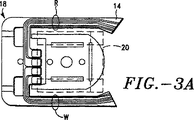
図3Aは、図3のフレクシャトレースアレイの読取/書込ヘッド接続領域の大幅に拡大された平面図であり、ヘッドスライダは破線の輪郭で示されている。
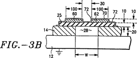
図3Bは、図3における線3B−3Bに沿う立面断面を大幅に拡大した図であり、この発明の原理に従いトレース対の2つの導電トレースを遮へいするための外側の誘電層上に形成される薄膜導電シールド(遮へい)を示す。
図4は、この発明の原理に従うトレースの対を遮へいするための一体化された浮動遮へい層を示す、図3Bと同様の図である。
図5は、この発明の原理に従いフレクシャ層で金属を堆積させることによりシールドを形成することを示す、図4と同様の図である。
図6は、この発明の原理に従いフレクシャ層で部分的にエッチングされたキャビティを形成することを示す、図4と同様の図である。
図7は、この発明の原理に従い誘電充填体材料で充填されたフレクシャ層で部分的にエッチングされたキャビティを形成することを示す、図4と同様の図である。
図8は、この発明の原理を取入れた、シングルエンドの配置において単一の導電トレースを遮へいするための外側の誘電層上に形成された薄い導電シールドを示す、図3Bと同様の図である。
好ましい実施例の詳細な説明
図面を参照すると、図面を通して同じ参照符号は同じまたは対応する部分を示しており、図1は、ハードディスクドライブ30のヘッド/ディスクアセンブリ(HDA)の平面図である。ハードディスクドライブ30は、フレクシャ14を備えるロードビーム12を含む少なくとも1つのロードビームアセンブリ10を用いる。フレクシャ14は、この発明の好ましい実施例として遮へいされたトレース相互接続アレイ16を含む。図1は、意図される動作環境内で用いられるフレクシャ14および遮へいされたトレース相互接続アレイ16を備えるロードビームアセンブリ10を示す。
この例では、ディスクドライブ30は、曲線で示された矢印の方向に少なくとも1つの記憶ディスク36を回転させるためのスピンドル34(およびスピンドルモータ(図示せず))を支持するための、たとえば固定ベース32を含む。ドライブ30はまた、回転するように旋回点35でベース32に取付けられた回転アクチュエータアセンブリ40を含む。アクチュエータアセンブリ40は、制御回路(図示せず)により選択的にエネルギが与えられたときにアクチュエータEブロック44およびヘッドアーム46(およびロードビームアセンブリ10)を移動させることによって対向する記憶ディスクの面上に定められた放射方向のトラック位置でこれらを位置決めする、音声コイル42を含む。ロードビームアセンブリ10の少なくとも1つは、基部側の端部17で、たとえば従来のボールスウェージ加工技術によりヘッドアーム46の末端側の端部に固定される。
必ずしも必要ではないが従来、2つのロードビームアセンブリ10がディスク36間においてヘッドアーム46に装着され、1つのロードビーム構造10が、スピンドル34において間隔が設けられた複数のディスク36からなるディスクの積み重ねのうちの最上部のディスクの上方でおよび最下部のディスクの下方でヘッドアームに取付けられる。トレース相互接続構造16は、Eブロック44の側部に固定されたたとえばセラミックハイブリッド回路基板52に延在する可撓性のトレース/膜セグメント50に接続する。セラミックハイブリッド回路52は読取プリアンプ/書込ドライバ回路を形成する半導体チップ54を固定および接続する。(ある応用例では、表面に載置されたIC54を備えるフレックス回路基板がセラミックハイブリッド回路基板52よりも好ましいことがある。)最も好ましくは、チップ54はハイブリッド回路52のセラミック基板およびEブロックの側壁との間で入れ子状にされ、適切な導電性接着剤または熱伝達化合物によりその側壁に固定されて、チップ54の動作中に生じる熱は伝導によりEブロックに放散し、対流により周囲空気体積へと外に向かって放散する。フレックス回路56は、基板52およびディスクドライブのその他の電子回路(図1には示さず)へのおよびそこからの電気接続を与える。
図2、3、3Aおよび3Bに示すように、ロードビームアセンブリ10は、総体的に平坦に形成されたステンレス鋼ロードビーム12と、長いフレクシャ14とを含む。この例では、フレクシャ14は、たとえば厚みがおよそ20−25ミクロンで最も好ましくは25ミクロンである薄いステンレス鋼シート材料からなる。導電トレース60および62は、間隔がおかれ総体的に並列な関係で形成され、厚みおよそ10−18ミクロンの銅の導体であり、最も好ましくは厚みは10ミクロンである。図3Bに示した導体トレース60および62は、たとえば、フレクシャ14の基部側の端部17でヘッド20の読取素子から、ロードビームアセンブリ10のスライダを支持する末端側の端部18に位置する別の接続パッドアレイ22へと延在する、相互接続構造16の読取経路導体トレース対を形成する。同様の導体トレース対が、ヘッド20の書込素子への接続のための書込経路Wを形成する。
好ましくは、導体トレース対RおよびWは、フレクシャの所望の機械的特性を損なわないように、対称をなすように形成されかつフレクシャ14の長手方向の端部に沿い長手方向の対称軸S(図3)を中心として間隔を設けられる。変換器ヘッドスライダ20(図3Aで破線の輪郭で示す)は、ロードビーム構造10の末端側の端部18で適切な接着剤によりジンバル14に取付けられる。図3Cに示すように、末端側の端部18における接続パッド22は、たとえば超音波溶接された金のボールボンド56により、スライダボディ20の後縁上に形成された二素子(4導体)薄膜磁気抵抗読取/薄膜誘導性書込構造26の整列した接続パッド24に接続するために与えられる。必ずしも必要ではないが好ましくは、スライダボディ20は30%ピコスライダである。
相互接続構造16は、ステンレス鋼フレクシャ14に取付けられた導体アレイ16の導電トレース60および62間に介在する高誘電性ポリイミド膜ベース25を含む。誘電層25の厚みはおよそ10−18ミクロンであり、最も好ましくは約10ミクロンである。誘電層25を、たとえばシルクスクリーニング、スピンコーティング、または精密ブレードまたはローラでのコーティングといった何らかの適切な方法により液体状態で与えてもよい。ポリイミドを備える接着剤によるように、ポリイミド誘電層25を与える他の方法は、この発明の意図する範囲内である。
共同発明者による、同一人に譲渡される1996年10月3日に出願され、「トリミングされたインピーダンスを有する一体化された導体を備えるサスペンション(Suspension with Integrated Conductors Having Trimmed Impedance)」と題された、米国特許出願第08/720,836号の開示を本明細書に引用により援用するが、この出願により教示されるように、フレクシャ14は読取/書込ヘッドのためのジンバル取付けを与えることに加え、好ましくは導体構造16の導電トレース60および62に関し制御された幅(w)および配置で1つ以上の開口部またはトラフ28を定める。フレクシャ14に沿い定められた長手方向の開口部28は、たとえば、導体構造のインダクタンス、キャパシタンスおよびラインインピーダンスの抵抗成分を、導体アレイ16に関する幅寸法(W)を変化させることにより同調させることを可能にする態様で、導体アレイ16に関して配置され間隔が取られる。
プリント回路導体は、より対線と同じ電気的自己遮へいの属性を有さないため、雑音が重要な要素となり得る。1996年10月3日に出願され、「自己遮へい一体化導体トレースアレイを備えるヘッドサスペンション(Head Suspension with Self-Shielding Integrated Conductor Trace Array)」と題された、同一人に譲渡される同時係属中の米国特許出願第08/724,978号は、書込導体トレースを読取トレース導体から離して配置するアレイレイアウトにより読取経路トレース導体を遮へいし得ることを開示している。しかしながら、たとえば図3に示すようにフレクシャ14の機械的対称性を保つことが必要だということは、実際にはフレクシャ14の対向する端部に沿い読取および書込導体の対RおよびWの経路を別々に取ることが最良であることを示唆している。この図3に示したトレース導体対の所望の対称配置は、読取トレース導体のシールド(遮へい)として書込トレース導体を用いることを効果的に除外する。
図3Bに示すように、この発明の原理に従うと、相互接続アレイ16は、好ましくは相互接続トレースアレイ16の2つの層において重なり合って整列するように配置された1対の導電トレース60および62を含む。第1の絶縁ポリイミド(可撓性重合樹脂材料)層25は、トレース60および62を薄いステンレス鋼フレクシャ14から分離する。ポリイミドの外側の絶縁誘電層70は、第1および第2のトレース60および62上に形成される。外側の誘電層70の厚みはたとえば3−14ミクロンであり、最も好ましくは、フレクシャ14に追加されるスチフネスを最小とするためには約3ミクロンである。外側のシールド(遮へい)72は、最も好ましくは、たとえば0.1から1.0ミクロンの厚みで(最も好ましくは約0.1ミクロン)外側のポリイミド層70上に薄膜金属層として堆積することにより形成される。薄膜堆積層72は、ステンレス鋼フレクシャ14との電気的接地コンタクトを取るために、外側の層70の横方向の端部を超え、内側の誘電層25の端部上まで続く。フレクシャ14の方では、Eブロックおよびアクチュエータ構造40を通してハードディスクドライブのベース32に接地されるロードビーム12に接地される。薄膜シールド層72を設けて、たとえば読取素子トレース導体対Rを含むトレース60および62を遮へいする。外側の誘電層70は内側の誘電層25と同様の誘電特性を有し、何らかの適切な方法で与えることができる。シールド薄膜層72は、好ましくは銅、銀、金またはステンレス鋼からなり、最も好ましくは銅の膜からなる。
図3Bに示すように、薄膜シールド(遮へい)72は、フレクシャ14に電気的に接地され、フレクシャ14の全体的な所望の機械特性に調和する適切な厚みを有することができる。薄膜シールド層72は接地されているため、各トレース60および62から共通の接地面へのキャパシタンスを増大する効果がある。この共通の接地面へのキャパシタンスは、参照する米国特許出願第08/720,836号の教示に従うパターニングされた反応性イオンエッチングまたはイオンミリングプロセスによるように、シールド72において長手方向に延在するウィンドウを定めることにより、減少させることができかつトレースアレイインピーダンスをトリミングすることができる。その代わりとして、共通接地面へのキャパシタンスは、フレクシャ14の所望の機械的特性が損なわれない限りは外側の誘電層70の厚みを減少させることによって減じることができる。
この発明の図4の例では、シールド72Aは誘電層25で終端をなし、したがって接地に関し電気的に浮動状態となる。この実施例では、シールド70Aの厚みは当該技術の電気設計者にとって重要な設計上の検討事項となる。たとえばもし、ある周波数fでの干渉信号または雑音の波頭が接地されていない導体シールド72Aに衝突すれば、波頭は以下の一次元近似に従い表皮深さδまで浸透するであろう。
![]()
図5の実施例では、シールド(遮へい)74は、たとえばフレクシャ14および/またはロードビーム12に電気的に接続される適切な厚みの金属膜のたとえば電着により、誘電層25に対して形成される。図6の例では、フレクシャ14Aは部分的にエッチングにより取除かれてキャビティ28Aを定める。図7の例では、フレクシャ14Bもまた部分的にエッチングによって取除かれ、結果として生じるキャビティは適切な誘電材料76によって充填される。
遮へいされたトレースアレイ構造は、フォトリソグラフィおよび選択性エッチングにより、または接着剤などを用いて導電トレースおよびシールドを誘電層に選択的堆積、積層または接着することによって、何らかの適切なパターニング技術を用いて形成される。このトレースアレイ構造は、被覆層72または72Aがロードビーム14と組合されかつこれと協働して読取対Rの2つの導電トレース60および62、および/または書込対Wの2つの導電トレースを遮へいするため、「2軸で遮へいされる」と言われる。トレース60および62は読取または書込素子のための好ましい信号経路として示されているが、図8の例において示されるように接地リターンシールド72Bを介してシングルエンドのまたは不平衡信号経路を形成する単一のトレース導体60を、本明細書において説明された技術により効果的に遮へいし得ることを当業者であれば認識するであろう。さらに、開示を本明細書に引用により援用する、1996年10月3日に出願され、「ハードディスクドライブにおけるR/Wヘッド相互接続のための多トレース伝送線路(Multi-trace Transmission Lines for R/W Head Interconnect in Hard Disk Drive)」と題された、同一人に譲渡される同時係属中の米国特許出願第08/726,450号により教示されるように、複数のトレースを並列の接続配置として設けてインダクタンスが減少した単一の信号経路を提供することができる。当業者ならば図4−8の断面図を見れば理解するであろうが、これらの断面図は非常に図式的なものであり、一定の率で示すことを意図したものではない。事実、実際のロードビーム12および/またはフレクシャ14の断面の幅は、この発明の原理を示すために提示したものであり実際の構成部品のための作業場用の図面を意図したものではないこれらの図面によって示されるものよりも、かなり大きくなる可能性がある。
この発明について、現在好ましい実施例すなわちジンバルを実現する堆積された導体フレクシャ構造という点から述べてきたが、当業者であれば、たとえば、近接して取付け、堆積または埋込まれた導体に絶縁の上塗りを施し遮へいを行なったものを備える一体化されたジンバルロードビーム構造またはその他の導電サスペンション部材と関連付けても利用できることが明白であろう。したがって、この開示は制限として解釈されるべきものではないことを理解する必要がある。当業者ならば上記開示を読めば種々の変形例および修正例が必ず明らかになるであろう。したがって、以下のクレームはこの発明の真の精神および範囲内のすべての変形例および修正例を包含するものとして解釈されることを意図している。 Reference to related applications
This application was filed on October 3, 1996, and “Suspension with Multi-Layered Integrated Conductor Trace Array for Optimized Electrical Parameters” This is a continuation-in-part of co-pending US patent application Ser. No. 08 / 720,833, the disclosure of which is hereby incorporated by reference.
Field of Invention
The present invention relates generally to a structure and method for electrically shielding a conductor trace array formed integrally with a head suspension assembly for use in a magnetic hard disk drive.
Background of the Invention
Modern magnetic hard disk drives typically define a number of concentric data storage tracks on each recording surface of the disk by positioning the rotating fixed storage disk and the data transducer at different radial locations with respect to the disk's rotational axis. Including a head positioner. The head positioner is generally called an actuator. A number of actuator structures are known in the art, but the most frequently used at present is the in-line rotary voice coil actuator because it is simple, high-performance and capable of mass balancing with respect to the rotating shaft. The latter is important for reducing the actuator's sensitivity to perturbations. Conventionally, the head is positioned with respect to the disk storage surface by operating the voice coil actuator using a closed loop servo system in the disk drive.
Read / write transducers, which may be single or two-element designs, are typically on a ceramic slider structure having an air bearing surface for supporting the transducer at a distance from the surface of the moving media. Provided. A single write / read element design typically requires a two-wire connection, and a two-element design with separate read and write elements requires two pairs of two-wire connections. In particular, magnetoresistive (MR) heads with separate inductive write elements generally require four wires. The combination of an air bearing slider and a read / write transducer is also known as a read / write head or recording head.
Generally, the slider is attached to a gimbal flexure structure that is mounted on the end of the suspension load beam structure on the distal side. While the spring biases the load beam and head toward the disk, the air pressure under the head caused by the rotation of the disk relative to the slider pushes the head away from the disk. The gimbal allows the slider to take a "flying" attitude toward the disk surface and follow its surface shape. The equilibrium distance defines the “air bearing” and determines the “flying height” of the head. By using an air bearing to support the head away from the disk surface, the head operates at the head / disk interface in a fluid lubrication situation rather than a boundary lubrication situation. Air bearings maintain the space between the transducer and the medium that reduces the efficiency of the transducer. However, avoiding direct contact greatly improves the reliability and useful life of the head and disk components. Nevertheless, the demand for increased area density may require the head to operate in pseudo contact or even in boundary lubricated contact situations.
Currently, the nominal flight height is on the order of 0.5 to 2 microinches. Magnetic storage density increases as the head approaches the storage surface of the disk. Thus, the very low flight height is at the expense of device reliability over the reasonable operational life of the disk drive. At the same time, data transfer rates to and from the storage surface are increasing and data rates approaching 200 megabits per second are within the actual planned range.
The disk drive industry has gradually reduced the size and mass of the slider structure to reduce the moving mass of the actuator assembly and allow the transducer to operate closer to the disk surface, while the former reduces seek performance. The latter, which leads to an increase in the efficiency of the converter that can be traded for a higher area density. Usually the size (and hence the mass) of the slider is characterized with reference to a so-called standard 100% slider (“mini slider”). Thus, the
In order to reduce this intrinsic wire stiffness or bias effect, the flexible insulation insulates the wire so that the conductor is exposed at a bonding pad positioned at the end of the flexure close to the head An integrated flexure / conductor structure that is effectively integrated with a resin flexure has been proposed. US Pat. No. 5,006,946 to Matsuzaki discloses an example of such a configuration. US Pat. No. 5,491,597 to Benin et al., US Pat. No. 4,761,699 to Ainslie et al., And US Pat. No. 4,996, to Erpelding et al. No. 623 discloses yet another example known in the art. While such a wiring configuration has some performance and assembly advantages, there are a number of difficult design problems in introducing a flexible polymeric resin material as disclosed into flexure and gimbal structures. For example, the thermal expansion properties of the resin material are not the same as the stainless steel structure according to the prior art, and the long-term durability of such a resin structure including some essential adhesive layer is unknown. Thus, a hybrid stainless steel flexure and conductor structure has been proposed that incorporates most of the advantages of an integrated conductor flex circuit flexure structure while remaining largely compatible with prior art manufacturing and load beam mounting methods. Yes. Such hybrid designs are typically provided in close proximity with preamplifier chips and downstream read channel circuits typically provided (along with other circuitry) on a circuit board mounted to the head / disk assembly. And using stainless steel flexures with insulating and conductive trace layers for electrical interconnection of the head to the associated drive electronics.
As taught by US Pat. No. 5,491,597 to Benin et al. Entitled “Gimbal Flexure and Electrical Interconnect Assembly”, the disclosed prior art strategy includes: This requires the use of a spring material for the conductive trace layer, such as, for example, a beryllium copper alloy that has a clearly higher electrical resistance than pure annealed copper. On the other hand, pure annealed copper is sufficient as an electrical conductor at high frequencies, but is more ductile rather than spring-like mechanical resilience and therefore lacks the mechanical spring properties desired for interconnect trace materials. For example, traces made of pure copper plated or deposited on a nickel base layer replace beryllium copper alloys on which Benin et al. Relies.
This hybrid flexure design consists of a pair of conductor traces or a set of four wires that extend relatively long from the bonding pad at the end of the flexure's distal head attached to the base end of the flexure. Used to provide a conductive path from the read / write head to the preamplifier or read channel chip along the length of the associated suspension structure. Since the conductor traces are positioned in close proximity to the flexure and in a generally parallel and spaced relationship, the exposed traces have thus far connected the read / write elements of each head to downstream processing electronics. Lacks the conventional fine twisted pair self-shielding properties used in Thus, the exposed traces tend to pick up unwanted signals that can distort or mask very low level signals induced in the read element of the head.
Microstrip line technology teaches that the loop and intra-conductor capacitance can be changed by changing the dimensions of the microstrips forming the transmission line and / or the spacing between the microstrips. However, in the case of an integrated trace array wiring method for use with a head suspension load beam, the conductor dimensions are subject to mechanical constraints including the space available on the flexure for the trace interconnect array, and the trace conductor The dimensions cannot be changed greatly as far as impedance matching or tuning is concerned.
Since printed circuit conductors do not have the twisted pair attribute, noise can be a factor affecting the electrical performance of the trace interconnect array. Previously assigned and co-pending U.S. patent application Ser. No. 08 / 724,978, filed Oct. 3, 1996, shields the read path conductive trace by using the write path conductive trace. Although it is taught that this may be the case, in practice this strategy may not be appropriate in some circumstances for structural reasons as opposed to electrical reasons. For example, in order to preserve the mechanical symmetry of the load beam structure, the read and write traces are separated so that they take separate paths along opposite longitudinal ends of the load beam. With such a symmetrical arrangement, the read trace cannot be blocked using the write trace. Therefore, improved trace conductor shielding in a conductor trace array used in the head mounting structure of a hard disk drive is necessary but has not yet been achieved.
Summary and purpose of the invention
A general object of the present invention is to provide a biaxial shielded integration for electrically interconnecting a read / write head to an associated read / write circuit that overcomes the limitations and disadvantages of the prior art. It is to provide a high performance suspension assembly having a low profile, strong and reliable with a conductor trace array.
Another general object of the present invention is to provide an integrated suspension and conductor structure that overcomes the limitations and disadvantages of the prior art by controlling the effectively shielded multilayer trace geometry. is there.
Another object of the present invention is an improved suspension and multilayer, biaxially shielded conductor trace array for supporting and electrically connecting read / write head elements provided on a slider in a hard disk drive. Is to provide.
A suspension assembly in accordance with the principles of the present invention includes a load beam and flexure for supporting a read / write head / slider assembly proximate a storage medium and electrically interconnecting the head to a read / write circuit. Including. The assembly is further arranged, for example, in a generally parallel and spaced relationship on the first electrical insulation layer forming a conductor trace pair with a first electrical insulation layer located on the flexure. First and second electrical signal trace paths, a second electrical insulation layer covering the conductor trace pair, and a conductor trace pair formed on the second electrical insulation layer to shield the electrical trace pair from external electrical interference A conductive shielding layer. In one preferred form, the shielding layer is grounded to the flexure. In another preferred form, the shielding layer is electrically floated with respect to the ground plane provided by the flexure, and the thickness of the shielding layer is greater than the depth of the skin effect at the frequency of the interference wave front.
In one related aspect of the invention, the first and second pairs of spaced and generally parallel signal trace paths are located along one longitudinal end region of the flexure where the first conductor trace pair is flexure. Formed on the flexure so that a second pair of conductor traces is formed along another longitudinal end region of the flexure that is transversely opposed to its one longitudinal end region. Thus, the second conductor trace pair is substantially symmetric with the first conductor trace pair with respect to the longitudinal symmetry axis.
The above and other objects, advantages, aspects and features of the present invention will be further appreciated and understood in consideration of the following detailed description of the preferred embodiments presented in conjunction with the accompanying drawings.
[Brief description of the drawings]
FIG. 1 is an enlarged plan view of a head disk assembly of a hard disk drive including an actuator having a suspension assembly with a shielded multilayer conductive trace array incorporating the principles of the present invention.
FIG. 2 is an enlarged plan view of an integrated flexure / conductor load beam structure included in the head disk assembly of FIG. 1 having shielded conductive traces in accordance with the principles of the present invention.
3 is an enlarged plan view of the flexure of the load beam structure of FIG. 2 having integrated wiring incorporating a tuned conductive trace array.
FIG. 3A is a greatly enlarged plan view of the read / write head connection area of the flexure trace array of FIG. 3, with the head slider shown with a dashed outline.
FIG. 3B is a greatly enlarged view of the elevational section along line 3B-3B in FIG. 3 formed on the outer dielectric layer for shielding the two conductive traces of the trace pair in accordance with the principles of the present invention. A thin film conductive shield (shield) is shown.
FIG. 4 is a view similar to FIG. 3B showing an integrated floating shielding layer for shielding a pair of traces according to the principles of the present invention.
FIG. 5 is a view similar to FIG. 4 showing the formation of a shield by depositing metal with a flexure layer in accordance with the principles of the present invention.
FIG. 6 is a view similar to FIG. 4 showing the formation of a partially etched cavity with a flexure layer in accordance with the principles of the present invention.
FIG. 7 is a view similar to FIG. 4 showing the formation of a partially etched cavity with a flexure layer filled with a dielectric filler material in accordance with the principles of the present invention.
FIG. 8 is a view similar to FIG. 3B showing a thin conductive shield formed on the outer dielectric layer for shielding a single conductive trace in a single-ended arrangement, incorporating the principles of the present invention. .
Detailed Description of the Preferred Embodiment
Referring to the drawings, like reference numerals designate like or corresponding parts throughout the views, and FIG. 1 is a plan view of a head / disk assembly (HDA) of a
In this example, the
Conventionally, but not necessarily, two
As shown in FIGS. 2, 3, 3A and 3B, the
Preferably, the conductor trace pairs R and W are formed symmetrically and do not impair the desired mechanical properties of the flexure and have a longitudinal symmetry axis S along the longitudinal end of the flexure 14 (see FIG. An interval is provided centering on 3). A transducer head slider 20 (shown in dashed outline in FIG. 3A) is attached to the
Filed on October 3, 1996 by the co-inventor and assigned to the same person, entitled “Suspension with Integrated Conductors Having Trimmed Impedance” No. 08 / 720,836, the disclosure of which is incorporated herein by reference, as taught by this application,
Noise can be an important factor because printed circuit conductors do not have the same electrical self-shielding attributes as twisted pairs. Filed October 3, 1996, entitled "Head Suspension with Self-Shielding Integrated Conductor Trace Array" US patent application Ser. No. 08 / 724,978 discloses that the read path trace conductors can be shielded by an array layout that places the write conductor traces away from the read trace conductors. However, the need to maintain the mechanical symmetry of the
In accordance with the principles of the present invention, as shown in FIG. 3B, the
As shown in FIG. 3B, the
In the example of FIG. 4 of the present invention,
![]()
In the embodiment of FIG. 5, a
The shielded trace array structure can be formed using any suitable patterning technique by photolithography and selective etching, or by selectively depositing, laminating or adhering conductive traces and shields to the dielectric layer using an adhesive or the like. It is formed. This trace array structure includes two
Although the present invention has been described in terms of a presently preferred embodiment, i.e., a deposited conductor flexure structure that provides a gimbal, those skilled in the art will be able to, for example, insulate closely mounted, deposited or embedded conductors. It will be apparent that it can also be used in conjunction with an integrated gimbal load beam structure or other conductive suspension member with a top coat and a shield. Accordingly, it should be understood that this disclosure is not to be construed as a limitation. Various alterations and modifications will no doubt become apparent to those skilled in the art after having read the above disclosure. Accordingly, the following claims are intended to be construed as including all variations and modifications within the true spirit and scope of this invention.
Claims (14)
前記ロードビーム上に配置され、前記読取/書込ヘッド/スライダアセンブリの近くまで延在する総体的に平坦な導電部材と、
前記導電部材上に形成される第1の電気絶縁層と、
前記第1の電気絶縁層上に形成される第1の電気信号トレース経路と、
前記第1の電気信号トレース経路上に形成される第2の電気絶縁層と、
前記第2の電気絶縁層上に形成され、前記第1の電気信号トレース経路を電気的干渉から遮へいするための導電遮へい層と、
前記導電部材によって前記第1の電気信号トレース経路の直下に定められる長手方向のウィンドウとを含み、前記長手方向のウィンドウの幅を選択して前記アセンブリの電気インピーダンスを制御する、一体化されたロードビームアセンブリ。An integrated load beam assembly including a load beam for supporting a read / write head / slider assembly proximate to a storage medium and electrically interconnecting the head to a read / write circuit comprising:
A generally flat conductive member disposed on the load beam and extending proximate to the read / write head / slider assembly;
A first electrical insulation layer formed on the conductive member;
A first electrical signal trace path formed on the first electrical insulation layer;
A second electrical insulation layer formed on the first electrical signal trace path;
A conductive shielding layer formed on the second electrical insulation layer for shielding the first electrical signal trace path from electrical interference;
An integrated load including a longitudinal window defined immediately below the first electrical signal trace path by the conductive member, the width of the longitudinal window being selected to control the electrical impedance of the assembly Beam assembly.
前記読取/書込ヘッド/スライダアセンブリを末端で支持する総体的に平坦に形成されたロードビームと、
前記ロードビーム上に配置され、前記読取/書込ヘッド/スライダアセンブリの近くまで延在する総体的に平坦な導電部材と、
前記導電部材上に配置される第1の電気絶縁層と、
前記第1の電気絶縁層上に配置される少なくとも1つの電気信号トレース経路と、
前記総体的に平坦な導電部材に接続され、前記少なくとも1つの電気信号トレース経路に重なり取囲む関係でかつ前記少なくとも1つの電気信号トレース経路から間隔をおいて配置されるシールドと、
前記導電部材によって前記少なくとも1つの電気信号トレース経路の直下に定められる長手方向のウィンドウとを含み、前記長手方向のウィンドウの幅を選択して前記アセンブリの電気インピーダンスを制御する、一体化されたロードビームアセンブリ。An integrated load beam assembly for supporting a read / write head / slider assembly proximate to a storage medium and for electrically interconnecting the head to a read / write circuit;
A generally flat load beam supporting the read / write head / slider assembly at its distal end;
A generally flat conductive member disposed on the load beam and extending proximate to the read / write head / slider assembly;
A first electrically insulating layer disposed on the conductive member;
At least one electrical signal trace path disposed on the first electrically insulating layer;
A shield connected to the generally flat conductive member and overlapping and surrounding the at least one electrical signal trace path and spaced from the at least one electrical signal trace path;
An integrated load including a longitudinal window defined immediately below the at least one electrical signal trace path by the conductive member, the width of the longitudinal window being selected to control the electrical impedance of the assembly Beam assembly.
前記読取/書込ヘッド/スライダアセンブリを支持するためのジンバルを有する総体的に平坦な導電フレクシャ部材と、
前記フレクシャ部材上に配置される第1の電気絶縁層と、
前記第1の電気絶縁層上に配置される第1および第2の電気信号トレース経路と、
前記第1および第2の電気信号トレース経路上に配置される第2の電気絶縁層と、
第2の電気絶縁層上に配置され、前記第1および第2の電気信号トレース経路を遮へいするための電気シールドと、
前記導電部材によって前記第1および第2の電気信号トレース経路の直下に定められる長手方向のウィンドウとを含み、前記長手方向のウィンドウの幅を選択して前記アセンブリの電気インピーダンスを制御し、
前記一体化されたフレクシャ/導体構造は前記ロードビーム上に配置されるので姿勢の低いサスペンションアセンブリが与えられる、一体化されたフレクシャ/導体構造。An integrated flexure / conductor structure for supporting a read / write head / slider assembly proximate to a storage medium on a load beam and electrically interconnecting the head to a read / write circuit;
A generally flat conductive flexure member having a gimbal for supporting the read / write head / slider assembly;
A first electrically insulating layer disposed on the flexure member;
First and second electrical signal trace paths disposed on the first electrical insulation layer;
A second electrical insulation layer disposed on the first and second electrical signal trace paths;
An electrical shield disposed on the second electrical insulation layer for shielding the first and second electrical signal trace paths;
A longitudinal window defined immediately below the first and second electrical signal trace paths by the conductive member, and selecting the width of the longitudinal window to control the electrical impedance of the assembly;
An integrated flexure / conductor structure that provides a low profile suspension assembly because the integrated flexure / conductor structure is disposed on the load beam.
Applications Claiming Priority (3)
| Application Number | Priority Date | Filing Date | Title |
|---|---|---|---|
| US08/785,570 US5796552A (en) | 1996-10-03 | 1997-01-21 | Suspension with biaxially shielded conductor trace array |
| US08/785,570 | 1997-01-21 | ||
| PCT/US1998/001197 WO1998034219A2 (en) | 1997-01-21 | 1998-01-20 | Suspension with biaxially shielded conductor trace array |
Publications (3)
| Publication Number | Publication Date |
|---|---|
| JP2000513861A JP2000513861A (en) | 2000-10-17 |
| JP2000513861A5 JP2000513861A5 (en) | 2005-07-14 |
| JP4070245B2 true JP4070245B2 (en) | 2008-04-02 |
Family
ID=25135909
Family Applications (1)
| Application Number | Title | Priority Date | Filing Date |
|---|---|---|---|
| JP53295598A Expired - Lifetime JP4070245B2 (en) | 1997-01-21 | 1998-01-20 | Suspension with biaxial shielded conductor trace array |
Country Status (5)
| Country | Link |
|---|---|
| US (1) | US5796552A (en) |
| EP (1) | EP0919053A4 (en) |
| JP (1) | JP4070245B2 (en) |
| AU (1) | AU5827698A (en) |
| WO (1) | WO1998034219A2 (en) |
Families Citing this family (73)
| Publication number | Priority date | Publication date | Assignee | Title |
|---|---|---|---|---|
| JP3206428B2 (en) * | 1996-04-09 | 2001-09-10 | ティーディーケイ株式会社 | Hard disk drive with head gimbal assembly |
| US5883758A (en) * | 1996-08-07 | 1999-03-16 | Hutchinson Technology Incorporated | Lead structure with stainless steel base for attachment to a suspension |
| US6147839A (en) * | 1996-12-23 | 2000-11-14 | Hutchinson Technology, Inc. | Head suspension with outriggers extending across a spring region |
| US5924187A (en) | 1998-01-06 | 1999-07-20 | Hutchinson Technology Incorporated | Integrated lead head suspension assembly having an etched laminated load beam and flexure with deposited conductors |
| US6025988A (en) * | 1998-12-17 | 2000-02-15 | Read-Rite Corporation | Interconnect adapter and head suspension assembly |
| US6487047B1 (en) | 1999-06-02 | 2002-11-26 | Maxtor Corporation | Trace interconnect array having increased bandwidth by selective etching of traces and dielectric substrate |
| US6480359B1 (en) | 2000-05-09 | 2002-11-12 | 3M Innovative Properties Company | Hard disk drive suspension with integral flexible circuit |
| US6639757B2 (en) * | 2001-01-10 | 2003-10-28 | Hutchinson Technology Inc. | Heat dissipation structures for integrated lead disk drive head suspensions |
| US6714385B1 (en) * | 2001-04-16 | 2004-03-30 | Hutchinson Technology Inc. | Apparatus and method for controlling common mode impedance in disk drive head suspensions |
| JP3929319B2 (en) * | 2002-02-01 | 2007-06-13 | 富士通株式会社 | Suspension and magnetic recording / reading apparatus |
| JP3891912B2 (en) * | 2002-10-09 | 2007-03-14 | 日本発条株式会社 | Disk drive suspension |
| US7158350B1 (en) | 2002-11-05 | 2007-01-02 | Hutchinson Technology Incorporated | Ground interconnects |
| WO2004084219A1 (en) * | 2003-03-17 | 2004-09-30 | Sae Magnetics (H.K) Ltd. | System and method for manufacturing a hard disk drive suspension flexure and for preventing damage due to electrical arcing |
| JP4222882B2 (en) * | 2003-06-03 | 2009-02-12 | 日東電工株式会社 | Printed circuit board |
| US7489479B2 (en) * | 2005-01-18 | 2009-02-10 | Hitachi Global Storage Technologies Netherlands B.V. | Electrical lead suspension having partitioned air slots |
| JP4640802B2 (en) * | 2005-07-07 | 2011-03-02 | 日東電工株式会社 | Suspension board with circuit |
| US7522382B1 (en) * | 2005-08-22 | 2009-04-21 | Western Digital (Fremont), Llc | Head stack assembly with interleaved flexure tail bond pad rows |
| US8553364B1 (en) | 2005-09-09 | 2013-10-08 | Magnecomp Corporation | Low impedance, high bandwidth disk drive suspension circuit |
| JP4615427B2 (en) * | 2005-12-01 | 2011-01-19 | 日東電工株式会社 | Printed circuit board |
| JP2008034639A (en) * | 2006-07-28 | 2008-02-14 | Nitto Denko Corp | Wired circuit board |
| JP4865453B2 (en) * | 2006-08-30 | 2012-02-01 | 日東電工株式会社 | Wiring circuit board and manufacturing method thereof |
| US7710687B1 (en) | 2006-09-13 | 2010-05-04 | Hutchinson Technology Incorporated | High conductivity ground planes for integrated lead suspensions |
| US7832082B1 (en) | 2006-10-10 | 2010-11-16 | Hutchinson Technology Incorporated | Method for manufacturing an integrated lead suspension component |
| US7929252B1 (en) | 2006-10-10 | 2011-04-19 | Hutchinson Technology Incorporated | Multi-layer ground plane structures for integrated lead suspensions |
| US7804663B2 (en) * | 2006-12-20 | 2010-09-28 | Hitachi Global Storage Technologies Netherlands B.V. | High frequency interconnect signal transmission lines |
| US7697237B1 (en) * | 2007-01-11 | 2010-04-13 | Hutchinson Technology Incorporated | Shielded copper-dielectric flexure for disk drive head suspensions |
| US7813084B1 (en) * | 2007-02-22 | 2010-10-12 | Hutchinson Technology Incorporated | Co-planar shielded write traces for disk drive head suspensions |
| US7986494B2 (en) * | 2007-05-04 | 2011-07-26 | Hutchinson Technology Incorporated | Integrated lead head suspension with tapered trace spacing |
| JP2008282995A (en) * | 2007-05-10 | 2008-11-20 | Nitto Denko Corp | Wiring circuit board |
| US20090113702A1 (en) * | 2007-11-01 | 2009-05-07 | Western Digital Technologies, Inc. | Disk drive comprising a double sided flex circuit wherein a first side lead provides an etching mask for a second side lead |
| JP2009188379A (en) * | 2008-01-07 | 2009-08-20 | Nitto Denko Corp | Wired circuit board |
| KR20090084512A (en) * | 2008-02-01 | 2009-08-05 | 삼성전자주식회사 | Suspension interconnect and head gimbal assembly with the same |
| JP2009246092A (en) * | 2008-03-31 | 2009-10-22 | Nitto Denko Corp | Wiring circuit board and method of manufacturing the same |
| US8169746B1 (en) | 2008-04-08 | 2012-05-01 | Hutchinson Technology Incorporated | Integrated lead suspension with multiple trace configurations |
| JP5091810B2 (en) * | 2008-09-03 | 2012-12-05 | 日東電工株式会社 | Wiring circuit board and manufacturing method thereof |
| WO2010026650A1 (en) * | 2008-09-05 | 2010-03-11 | 東芝ストレージデバイス株式会社 | Head suspension unit and head suspension assembly |
| US8289656B1 (en) | 2008-11-19 | 2012-10-16 | Western Digital Technologies, Inc. | Disk drive comprising stacked and stepped traces for improved transmission line performance |
| US8045297B2 (en) * | 2008-11-25 | 2011-10-25 | Hitachi Global Storage Technologies, Netherlands B.V. | Flex cable and method for lowering flex cable impedance |
| US8462466B2 (en) * | 2009-08-31 | 2013-06-11 | Western Digital Technologies, Inc. | Disk drive comprising impedance discontinuity compensation for interconnect transmission lines |
| JP5377177B2 (en) * | 2009-09-08 | 2013-12-25 | 日本発條株式会社 | Suspension for disk unit |
| US8542465B2 (en) | 2010-03-17 | 2013-09-24 | Western Digital Technologies, Inc. | Suspension assembly having a microactuator electrically connected to a gold coating on a stainless steel surface |
| JP6021211B2 (en) * | 2010-04-30 | 2016-11-09 | 大日本印刷株式会社 | Suspension board, suspension, suspension with element, and hard disk drive |
| US8467151B1 (en) | 2010-05-21 | 2013-06-18 | Western Digital Technologies, Inc. | Disk drive comprising an interconnect with transmission lines forming an approximated lattice network |
| US8885299B1 (en) | 2010-05-24 | 2014-11-11 | Hutchinson Technology Incorporated | Low resistance ground joints for dual stage actuation disk drive suspensions |
| US8665567B2 (en) | 2010-06-30 | 2014-03-04 | Western Digital Technologies, Inc. | Suspension assembly having a microactuator grounded to a flexure |
| JP5583539B2 (en) * | 2010-10-01 | 2014-09-03 | 日本発條株式会社 | Flexure wiring structure |
| JP5762119B2 (en) * | 2011-05-06 | 2015-08-12 | 日東電工株式会社 | Suspension board with circuit and manufacturing method thereof |
| JP5924909B2 (en) | 2011-11-21 | 2016-05-25 | 日東電工株式会社 | Wiring circuit board and manufacturing method thereof |
| JP5349634B2 (en) * | 2012-03-16 | 2013-11-20 | 日東電工株式会社 | Suspension board with circuit |
| WO2013138619A1 (en) | 2012-03-16 | 2013-09-19 | Hutchinson Technology Incorporated | Mid-loadbeam dual stage actuated (dsa) disk drive head suspension |
| CN104205216A (en) | 2012-03-22 | 2014-12-10 | 哈特奇桑科技公司 | Ground feature for disk drive head suspension flexures |
| US8861141B2 (en) | 2012-08-31 | 2014-10-14 | Hutchinson Technology Incorporated | Damped dual stage actuation disk drive suspensions |
| WO2014043498A2 (en) | 2012-09-14 | 2014-03-20 | Hutchinson Technology Incorporated | Co-located gimbal-based dual stage actuation disk drive suspensions |
| JP6356682B2 (en) | 2012-10-10 | 2018-07-11 | ハッチンソン テクノロジー インコーポレイテッドHutchinson Technology Incorporated | Suspension with two-stage operation structure |
| US8941951B2 (en) | 2012-11-28 | 2015-01-27 | Hutchinson Technology Incorporated | Head suspension flexure with integrated strain sensor and sputtered traces |
| US8891206B2 (en) | 2012-12-17 | 2014-11-18 | Hutchinson Technology Incorporated | Co-located gimbal-based dual stage actuation disk drive suspensions with motor stiffener |
| US8896969B1 (en) | 2013-05-23 | 2014-11-25 | Hutchinson Technology Incorporated | Two-motor co-located gimbal-based dual stage actuation disk drive suspensions with motor stiffeners |
| US8717712B1 (en) | 2013-07-15 | 2014-05-06 | Hutchinson Technology Incorporated | Disk drive suspension assembly having a partially flangeless load point dimple |
| US8792214B1 (en) | 2013-07-23 | 2014-07-29 | Hutchinson Technology Incorporated | Electrical contacts to motors in dual stage actuated suspensions |
| US8675314B1 (en) | 2013-08-21 | 2014-03-18 | Hutchinson Technology Incorporated | Co-located gimbal-based dual stage actuation disk drive suspensions with offset motors |
| US8879212B1 (en) | 2013-08-23 | 2014-11-04 | Western Digital Technologies, Inc. | Disk drive suspension assembly with flexure having dual conductive layers with staggered traces |
| US8988829B1 (en) | 2013-09-18 | 2015-03-24 | HGST Netherlands B.V. | Disk drive with preamplifier for multiple readers in a slider with a common return signal |
| US9330693B1 (en) | 2013-09-27 | 2016-05-03 | Magnecomp Corporation | Suspension circuit trace employing stacked traces and windowed stainless steel layer |
| US8896970B1 (en) | 2013-12-31 | 2014-11-25 | Hutchinson Technology Incorporated | Balanced co-located gimbal-based dual stage actuation disk drive suspensions |
| US8867173B1 (en) | 2014-01-03 | 2014-10-21 | Hutchinson Technology Incorporated | Balanced multi-trace transmission in a hard disk drive flexure |
| US9070392B1 (en) | 2014-12-16 | 2015-06-30 | Hutchinson Technology Incorporated | Piezoelectric disk drive suspension motors having plated stiffeners |
| US9318136B1 (en) | 2014-12-22 | 2016-04-19 | Hutchinson Technology Incorporated | Multilayer disk drive motors having out-of-plane bending |
| US9296188B1 (en) | 2015-02-17 | 2016-03-29 | Hutchinson Technology Incorporated | Partial curing of a microactuator mounting adhesive in a disk drive suspension |
| US9218822B1 (en) | 2015-05-13 | 2015-12-22 | HGST Netherlands B.V. | Disk drive with preamplifier with isolation for multiple readers in a slider with a common return signal |
| WO2017003782A1 (en) | 2015-06-30 | 2017-01-05 | Hutchinson Technology Incorporated | Disk drive head suspension structures having improved gold-dielectric joint reliability |
| US9646638B1 (en) | 2016-05-12 | 2017-05-09 | Hutchinson Technology Incorporated | Co-located gimbal-based DSA disk drive suspension with traces routed around slider pad |
| JP6808266B2 (en) * | 2016-05-18 | 2021-01-06 | 日東電工株式会社 | Wiring circuit board and its manufacturing method |
| JP6802688B2 (en) * | 2016-11-02 | 2020-12-16 | 日東電工株式会社 | Wiring circuit board |
Family Cites Families (16)
| Publication number | Priority date | Publication date | Assignee | Title |
|---|---|---|---|---|
| US4819094A (en) * | 1986-08-12 | 1989-04-04 | Oberg Gary R | Damped magnetic head suspension assembly |
| US4761699A (en) * | 1986-10-28 | 1988-08-02 | International Business Machines Corporation | Slider-suspension assembly and method for attaching a slider to a suspension in a data recording disk file |
| US5001583A (en) * | 1989-04-19 | 1991-03-19 | Tdk Corporation | Flexible polymeric resinous magnetic head supporting device |
| US5006946A (en) * | 1989-04-19 | 1991-04-09 | Tdk Corporation | Flexible polymeric resinous magnetic head supporting device |
| US4996623A (en) * | 1989-08-07 | 1991-02-26 | International Business Machines Corporation | Laminated suspension for a negative pressure slider in a data recording disk file |
| US5021907A (en) * | 1989-12-11 | 1991-06-04 | Seagate Technology, Inc. | Gimbal spring for supporting a magnetic transducer and making electrical contact therewith |
| US5391842A (en) * | 1991-12-16 | 1995-02-21 | Hutchinson Technology, Inc. | Carrier strip head interconnect assembly |
| JP2616631B2 (en) * | 1992-04-23 | 1997-06-04 | 日本電気株式会社 | Magnetic head |
| US5292268A (en) * | 1992-08-05 | 1994-03-08 | Burndy Corporation | Controlled impedance shield for an electrical connector |
| JP2881188B2 (en) * | 1993-07-12 | 1999-04-12 | 株式会社日立製作所 | Rotating disk storage device and its head suspension |
| JP2935802B2 (en) * | 1993-12-09 | 1999-08-16 | アルプス電気株式会社 | Levitated magnetic head device |
| US5491597A (en) * | 1994-04-15 | 1996-02-13 | Hutchinson Technology Incorporated | Gimbal flexure and electrical interconnect assembly |
| US5530604A (en) * | 1994-05-19 | 1996-06-25 | International Business Machines Corporation | Electrical connection and slider-suspension assembly having an improved electrical connection |
| JP2855254B2 (en) * | 1994-07-15 | 1999-02-10 | 日本メクトロン株式会社 | Method of manufacturing suspension for magnetic head with circuit wiring |
| US5608591A (en) * | 1995-06-09 | 1997-03-04 | International Business Machines Corporation | Integrated head-electronics interconnection suspension for a data recording disk drive |
| US5754369A (en) | 1996-10-03 | 1998-05-19 | Quantum Corporation | Head suspension with self-shielding integrated conductor trace array |
-
1997
- 1997-01-21 US US08/785,570 patent/US5796552A/en not_active Expired - Lifetime
-
1998
- 1998-01-20 WO PCT/US1998/001197 patent/WO1998034219A2/en active Application Filing
- 1998-01-20 AU AU58276/98A patent/AU5827698A/en not_active Abandoned
- 1998-01-20 EP EP98901850A patent/EP0919053A4/en not_active Ceased
- 1998-01-20 JP JP53295598A patent/JP4070245B2/en not_active Expired - Lifetime
Also Published As
| Publication number | Publication date |
|---|---|
| WO1998034219A3 (en) | 1998-11-19 |
| AU5827698A (en) | 1998-08-25 |
| WO1998034219A2 (en) | 1998-08-06 |
| EP0919053A4 (en) | 2008-04-30 |
| EP0919053A2 (en) | 1999-06-02 |
| JP2000513861A (en) | 2000-10-17 |
| US5796552A (en) | 1998-08-18 |
Similar Documents
| Publication | Publication Date | Title |
|---|---|---|
| JP4070245B2 (en) | Suspension with biaxial shielded conductor trace array | |
| US6038102A (en) | Conductor trace array having interleaved passive conductors | |
| JP3945873B2 (en) | Integral load beam assembly and integral bend / conductor structure | |
| US6275358B1 (en) | Conductor trace array having passive stub conductors | |
| US5812344A (en) | Suspension with integrated conductor trace array having optimized cross-sectional high frequency current density | |
| US5995328A (en) | Multi-layered integrated conductor trace array interconnect structure having optimized electrical parameters | |
| US5608591A (en) | Integrated head-electronics interconnection suspension for a data recording disk drive | |
| JP3974694B2 (en) | Integral self-shielding bend / conductor structure and disk drive | |
| JPH097146A (en) | Combined assembly of converter, sliding part and suspension part and its manufacture | |
| WO1998020485A1 (en) | Head suspension with self-shielding 'twisted' integrated conductor trace array | |
| US7046483B2 (en) | Copper gimbal and gimbal damping for integrated lead suspension | |
| US6731467B1 (en) | Trace interconnect array having increased bandwidth by selective etching of traces and dielectric substrate | |
| KR19990021924A (en) | Suspension with integrated conductor with controlled capacitance | |
| WO1998014937A1 (en) | Suspension with integrated conductors having trimmed impedance | |
| US7099118B2 (en) | One-piece suspension assembly including interconnect |
Legal Events
| Date | Code | Title | Description |
|---|---|---|---|
| A521 | Request for written amendment filed |
Free format text: JAPANESE INTERMEDIATE CODE: A523 Effective date: 20041102 |
|
| A621 | Written request for application examination |
Free format text: JAPANESE INTERMEDIATE CODE: A621 Effective date: 20041102 |
|
| TRDD | Decision of grant or rejection written | ||
| A01 | Written decision to grant a patent or to grant a registration (utility model) |
Free format text: JAPANESE INTERMEDIATE CODE: A01 Effective date: 20071218 |
|
| A61 | First payment of annual fees (during grant procedure) |
Free format text: JAPANESE INTERMEDIATE CODE: A61 Effective date: 20080115 |
|
| R150 | Certificate of patent or registration of utility model |
Free format text: JAPANESE INTERMEDIATE CODE: R150 |
|
| FPAY | Renewal fee payment (event date is renewal date of database) |
Free format text: PAYMENT UNTIL: 20110125 Year of fee payment: 3 |
|
| FPAY | Renewal fee payment (event date is renewal date of database) |
Free format text: PAYMENT UNTIL: 20110125 Year of fee payment: 3 |
|
| S111 | Request for change of ownership or part of ownership |
Free format text: JAPANESE INTERMEDIATE CODE: R313113 |
|
| FPAY | Renewal fee payment (event date is renewal date of database) |
Free format text: PAYMENT UNTIL: 20110125 Year of fee payment: 3 |
|
| R350 | Written notification of registration of transfer |
Free format text: JAPANESE INTERMEDIATE CODE: R350 |
|
| FPAY | Renewal fee payment (event date is renewal date of database) |
Free format text: PAYMENT UNTIL: 20120125 Year of fee payment: 4 |
|
| FPAY | Renewal fee payment (event date is renewal date of database) |
Free format text: PAYMENT UNTIL: 20130125 Year of fee payment: 5 |
|
| R250 | Receipt of annual fees |
Free format text: JAPANESE INTERMEDIATE CODE: R250 |
|
| R250 | Receipt of annual fees |
Free format text: JAPANESE INTERMEDIATE CODE: R250 |
|
| R250 | Receipt of annual fees |
Free format text: JAPANESE INTERMEDIATE CODE: R250 |
|
| R250 | Receipt of annual fees |
Free format text: JAPANESE INTERMEDIATE CODE: R250 |
|
| EXPY | Cancellation because of completion of term |