JP4067164B2 - Polishing method and polishing apparatus - Google Patents
Polishing method and polishing apparatus Download PDFInfo
- Publication number
- JP4067164B2 JP4067164B2 JP06434498A JP6434498A JP4067164B2 JP 4067164 B2 JP4067164 B2 JP 4067164B2 JP 06434498 A JP06434498 A JP 06434498A JP 6434498 A JP6434498 A JP 6434498A JP 4067164 B2 JP4067164 B2 JP 4067164B2
- Authority
- JP
- Japan
- Prior art keywords
- polishing
- polished
- torque
- uniformity
- wafer
- Prior art date
- Legal status (The legal status is an assumption and is not a legal conclusion. Google has not performed a legal analysis and makes no representation as to the accuracy of the status listed.)
- Expired - Fee Related
Links
Images


Description
【0001】
【発明の属する技術分野】
本発明は、半導体素子、磁性素子、光学素子など薄膜素子の製造工程において、平面基板上に形成された薄膜の表面平坦化などに用いられる研磨方法及び研磨装置に関し、特にLSI等の半導体素子の製造工程においてシリコンウエハの表面に形成された薄膜の表面平坦化に用いられる研磨方法及び研磨装置に関する。
【0002】
【従来の技術】
近年、例えばLSI等の半導体素子の製造工程において、半導体素子の高密度化を目的として多層配線が用いられるようになり、また半導体素子の微細化に伴い配線形成の高密度化が要求されるようになってきている。そのため、例えば層間絶縁膜や配線となる導電膜をウエハ表面に形成した後、これらの薄膜の表面の凹凸を化学的機械研磨(CMP:Chemical Mechanical Polishing) により平坦化することが行われるようになってきている。
【0003】
このウエハ表面の薄膜の研磨には、研磨台に載置されたウエハに、研磨定盤に取り付けられた研磨パッドを押し当て、研磨スラリ(砥粒液)を供給しながら、研磨台および研磨定盤のいずれか一方または両方を回転させる方法が採られている。複数枚のウエハを研磨台に載置することにより、各ウエハを同時に研磨することも行われる。
【0004】
従来、CMP装置により、層間絶縁膜を研磨除去して薄膜表面の凹凸を平坦化するに際して、研磨が下地膜(下層の配線)まで達して、さらに下地膜を研磨し過ぎた場合、短絡などの配線不良が生じ、製造される半導体の特性に影響を与える。
【0005】
さらに、複数枚のウエハを同時に研磨する場合は、研磨部は各ウエハの全面であるため、各ウエハ面内で均一に、かつ各ウエハ間でも同一の研磨厚みに研磨除去することが必要である。
【0006】
通常、このような研磨を可能にするため、各ウエハの薄膜の初期厚みを同一とし、ウエハ面内で研磨の均一性が良く、しかも薄膜の下地膜に対する選択比が大きい研磨条件で、薄膜を研磨することが行われている。この場合には、すべての研磨面を下地膜の表面に到達させるべく研磨時間を少し長くしたとしても、下地膜に対する選択比が大きいので、下地膜が研磨される量を抑えることができる。ここで選択比とは、研磨速度の比をいう。
【0007】
【発明が解決しようとする課題】
以上のような従来の研磨装置及び研磨方法によれば、一般に、研磨する条件を一定にしていても、研磨パッドやリテーナなどの研磨部品の損耗や研磨条件の外乱による変動、および研磨する薄膜の状態などが一定ではないため、ウエハ面内およびまたは複数のウエハ間の研磨の均一性は変化する。
【0008】
そのため、ウエハ面内での研磨の均一性および下地膜に対する選択比を満足する研磨条件を選択していたとしても、研磨が良好に行われない場合がある。従って、研磨バッチ毎に研磨の均一性を確認することが望ましい。しかし、すべての研磨に対して膜厚測定器を用いてウエハ面内およびまたはウエハ間の研磨の均一性を確認することは商業的な生産では困難である。
【0009】
そこで本発明は、ウエハ面内の研磨の均一性や複数のウエハ間の研磨の均一性を容易に評価できる研磨方法とそのような研磨装置を提供することを目的としている。さらに、ウエハ面内の研磨の均一性や複数のウエハ間の研磨の均一性の悪化を直ちに判定することにより、長期にわたって良好な研磨が可能な研磨方法及びそのような研磨装置を提供することを目的としている。
【0010】
【課題を解決するための手段】
上記目的を達成するために、請求項1に係る発明による研磨方法は、被研磨物の被研磨面に研磨パッドを押し当て、前記被研磨物および前記研磨パッドの少なくとも一方を回転させて前記被研磨物を研磨する研磨方法であって、前記研磨パッドを回転させる回転トルクおよび前記被研磨物を回転させる回転トルクの少なくとも一方の回転トルクの時間変化率を検出し、検出された回転トルクの時間変化率に基づいて前記被研磨面の研磨均一性を評価することを特徴とする。また、請求項2に係る発明による研磨方法は、前記被研磨物は複数であることを特徴とする。ここで、例えば図2を参照すれば、研磨パッド2を回転させる回転トルクは、回転軸23の回転トルクであり、被研磨物Sを回転させる回転トルクは、回転軸21または回転軸22の回転トルクである。また、検出されたトルクの時間変化率に基づいて被研磨面Saの研磨均一性を評価するには、例えば実験によりトルクの時間変化率と被研磨面Sa内の研磨均一性との相関関係を把握しておき、それと実際に計測されるトルクの時間変化率とを比較する。
【0011】
このように構成すると、検出されたトルクの時間変化率に基づいて被研磨面Saの研磨均一性を評価するので、被研磨物の複数の測定点における膜厚を直接計測することなく研磨均一性をトルクの時間変化率から間接的に確実に知ることができる。
【0012】
なお、図1〜図3に示すように、複数の被研磨物Sの被研磨面Saに研磨パッド2を押し当て、複数の被研磨物Sをそれぞれ自転させると共に、複数の被研磨物Sと研磨パッド2とを相対的に公転させて複数の被研磨物Sを研磨する研磨方法であって、相対的に公転させるための回転トルクと複数の被研磨物Sをそれぞれ自転させる各回転トルクの少なくとも一つの回転トルクの時間変化率を検出し、前記検出されたトルクの時間変化率に基づいて被研磨面Saの研磨均一性を評価するようにしてもよい。ここで、被研磨面Saの研磨均一性というときは、ある1つの被研磨面Sa内の研磨の均一性、あるいは複数の被研磨面Sa間の研磨の均一性を意味する。また、例えば図2を参照すれば、相対的に公転させるための回転トルクは、回転軸22または回転軸23の回転トルクであり、自転させる各回転トルクは各回転軸21の回転トルクである。
【0013】
このように構成すると、相対的に公転させるための回転軸22あるいは回転軸23と複数の被研磨物Sをそれぞれ自転させる各回転軸21の少なくとも一つの回転軸のトルクの時間変化率に基づいて研磨均一性を評価するので、特に回転軸22あるいは回転軸23のトルクを用いるときは複数の同時に研磨されている被研磨物S全体の被研磨面Sa内の平均的な研磨均一性が評価でき、各回転軸21のトルクを用いるときは、複数の被研磨物Sの各被研磨面Sa内の研磨均一性が評価できる他、複数の被研磨物Sの各被研磨面Sa間の研磨の均一性が評価できる。
【0014】
以上の研磨方法では、請求項3に記載のように、被研磨物Sと研磨パッド2との間に研磨スラリを供給するようにしてもよい。このときは、特にCMPによる研磨方法として用いることができる。
【0015】
以上の研磨方法では、請求項4に記載のように、前記評価された研磨均一性に基づいて研磨条件を設定するようにしてもよい。
【0016】
このときは、評価された研磨均一性に基づいて研磨条件を設定するので、ウエハ面内あるいはウエハ間の研磨の進行が不均一と判明したとき、それを修正するように研磨条件を変更できる。
【0017】
請求項5に記載のように、請求項4に記載の研磨方法においては、前記研磨条件の設定は、前記研磨パッドの回転数の変更、前記被研磨物の回転数の変更、前記研磨パッドを前記被研磨面に押しつける圧力の変更、前記研磨スラリの流量の変更、前記研磨パッドの交換、前記被研磨物を保持するリテーナの調整(例えばシムの挿入等による高さの変更)、前記被研磨物を保持するリテーナの交換、及び前記研磨パッドの目立ての実施の少なくとも1つであるようにすることが好ましい。これらの条件が、ウエハSの研磨均一性を支配する主なものである。ここで例えば図2を参照すれば、研磨パッド2の回転数とは回転軸23の回転数であり、被研磨物Sの回転数とは回転軸21あるいは回転軸22の回転数である。
【0018】
上記目的を達成するために、請求項6に係る発明による研磨装置は、被研磨物が取り付けられて一の回転軸回りに回転する研磨台と、前記研磨台に取り付けられた被研磨物に押し当てられて前記被研磨物を研磨する研磨パッドと、前記研磨パッドを被着して、他の回転軸回りに回転する研磨定盤と、各回転軸のうち少なくとも1つの回転軸のトルクの時間変化率を検出するトルク時間変化率検出部と、前記トルク時間変化率検出部で検出されたトルクの時間変化率に基づいて前記被研磨面の研磨均一性を評価する評価部とを備える。トルク時間変化率検出部と評価部とは一体の装置として構成してもよい。また、請求項7に係る発明による研磨装置は、被研磨物の被研磨面に研磨パッドを押し当て、前記被研磨物および前記研磨パッドの少なくとも一方を回転させて前記被研磨物を研磨する研磨装置であって、前記研磨パッドを回転させる回転トルクおよび前記被研磨物を回転させる回転トルクの少なくとも一方の回転トルクの時間変化率を検出する手段と、検出された回転トルクの時間変化率に基づいて前記被研磨面の研磨均一性を評価する手段とを備えることを特徴とする。
【0019】
このように構成すると、特に回転軸22あるいは回転軸23のトルクを用いるときは複数の被研磨物S全体の被研磨面Sa内の平均的な研磨均一性が評価でき、各回転軸21のトルクを用いるときは、被研磨物S全体の被研磨面Sa内の研磨均一性を評価することもでき、さらには複数の被研磨物Sの各被研磨面Sa内の研磨の均一性の他、複数の被研磨物Sの各被研磨面Sa間の研磨の均一性も評価できる。
【0020】
上記の研磨装置では、請求項8に記載のように、評価された研磨均一性に基づいて研磨条件を設定する手段を備えてもよい。
【0021】
このように構成すると、研磨条件設定部10(20)が評価部9(19)で評価された研磨均一性に基づいて、研磨不良を修正するように研磨条件を設定することができる。
【0022】
【発明の実施の形態】
以下、本発明の実施の形態について、図面を参照して説明する。なお、各図において互いに同一あるいは相当する部材には同一符号を付し、重複した説明は省略する。
【0023】
本発明者らは、研磨の終点検知の一つの方法 として用いられている研磨時のトルク変化に着目し、さらに、そのトルクの時間変化率を用いて、以下の知見に基づいて本発明を完成させた。
【0024】
研磨台上にて複数枚の被研磨物であるウエハを同時に研磨する構造の研磨装置において、研磨されるウエハの層間絶縁膜は一般的には2層以上の構造であり、その上・下層の薄膜は研磨抵抗が異なるのが普通である。図9に層間絶縁膜の構造の一例を断面図で示す。
【0025】
図9に示す層間絶縁膜は、シリコン等のウエハ基板SAの上に配線SX1が形成され、その配線同士の間が配線間絶縁膜SBで埋められている。これらを形成するにあたっては、先ずウエハ基板SAの上に配線SX1が形成され、その上を覆うように配線間絶縁膜SBが堆積され、その後、配線間絶縁膜SBが配線SX1の高さと同一の高さまで研磨除去され、配線SX1の上部が配線間絶縁膜SBから露出して、全体として平坦な面となるようにする。
【0026】
その平坦な面の上に第1層の層間絶縁膜SCが堆積され、その上面は研磨され平坦面となり、その平坦面上に第2の配線SX2が形成され、その上を覆うように配線間絶縁膜SDが堆積され、その後、配線間絶縁膜SDが配線SX2の高さと同一の高さまで研磨除去され、配線SX2の上部が配線間絶縁膜SDから露出して、全体として平坦な面となるように加工される。図9では、配線間絶縁膜SDは未だ研磨除去されておらず、研磨除去されて平坦な面となるところが破線で表示されている。即ち配線SX2の上部が露出する高さである。
【0027】
図9に示される配線SX1と配線間絶縁膜SBの上面のような多層絶縁膜構造の研磨終点の検知では、上層が研磨除去されて下層が現れた時の研磨抵抗の差異を、研磨トルクが減少または増加することを利用して検知し、研磨終点を判定している。
【0028】
ここで、研磨トルクは、上層の薄膜が除去されて、下層の薄膜が出現してくる時の下層の薄膜の出現面積にほぼ比例して変化する。従って、ウエハ面内およびウエハ間で研磨が均一に進行している場合、1つのウエハ面内および複数のウエハ間の各部でほぼ同時に研磨対象の薄膜が除去されて下地膜が露出する。その結果、下地膜の面積が急速に増加するので、研磨終点近傍でのトルクの減少率または増加率、即ちトルクの時間変化率が大きくなる。
【0029】
一方、1つのウエハ面内や複数のウエハ間で研磨が均一に進行していない場合、ウエハ面内およびまたはウエハ間の各部で研磨対象の薄膜が除去されて下地膜が露出する時期がずれる。その結果、下地膜の面積の増加は緩やかなものとなり、研磨終点近傍でのトルクの時間変化率が小さくなる。
【0030】
図4のトルク変化の模式図を参照して、上層薄膜の研磨抵抗が下層薄膜より大きい場合について、研磨進行に伴うトルク変化を説明する。
【0031】
ウエハ面内の研磨が均一に進行している場合(図中○の場合)、研磨終点(図中EP)近傍のトルクの時間に対する減少勾配、即ちトルクの時間変化率は急激である。これに対して、ウエハ面内の研磨が不均一に進行している場合(図中△および□の場合)、研磨の均一性が悪くなるに従い、研磨終点近傍でのトルクの減少勾配は緩やかになる。
【0032】
図4のような線図を複数のウエハのそれぞれについて作成すると、複数のウエハ各々の面内の研磨が均一で複数のウエハ間の研磨が不均一に進行している場合は、各線図でのトルクの減少勾配は急であるが、研磨終点EPの時間位置が線図毎にずれる。
【0033】
また複数のウエハを総合した全体としての研磨均一性を示す線図を作成すると(研磨台の回転軸あるいは研磨定盤の回転軸のトルクを測定して)、複数のウエハ各々の面内の研磨均一性が悪いか、各ウエハ間の研磨均一性が悪いと、やはりトルクの減少勾配は緩やかになる。この場合、複数のウエハ各々の面内の研磨均一性が良好で、かつ各ウエハ間の研磨均一性も良好であれば、トルクの減少勾配は急になる。
【0034】
図5に、上層の研磨抵抗が下層より小さい場合について、研磨進行に伴うトルク変化の模式図を示す。
【0035】
ウエハ面内の研磨が均一に進行している場合(図中○の場合)、研磨終点(図中EP)近傍のトルクの増加勾配、即ちトルクの時間変化率は急激である。これに対して、ウエハ面内の研磨が不均一に進行している場合(図中△および□の場合)、研磨の均一性が悪くなるに従い、研磨終点近傍でのトルクの増加勾配は緩やかになる。
【0036】
図5のような線図を複数のウエハのそれぞれについて作成した場合の知見については、図4の場合と同様なので重複した説明は省略する。
【0037】
この研磨トルクの時間変化率(時間に対する1次微分値)の大小によって1つのウエハの被研磨面内およびまたは複数のウエハ間の研磨の均一性を定量化することができ、ひいてはそのような研磨の均一性を評価することができる。そして、研磨が良好に行われたかどうかを容易に判定することができる。
【0038】
以下図面を参照して、本発明の実施の形態について説明する。図1は、本発明の第1の実施の形態であるCMPによる研磨装置の斜視図であり、図2は図1の研磨装置の一部を断面した拡大断面図であり、図3は図1の装置の被研磨物載置部を搭載する研磨台の平面図(図2のA−A矢視図)である。
【0039】
図1及び図2において、研磨パッド2を被着する円盤状の研磨定盤5が、被着面を下方に向けて、またその円盤の中心で円盤の上方に円盤に垂直に設けられた第3の回転軸である回転軸23の回りに回転するように構成されている。研磨定盤5の研磨パッド2を被着する面は、回転軸23の回転軸線を中心とする円環状の平面になっており、その面に密着させて円環状の弾性体でできた弾性円盤14が搭載され、弾性円盤14を覆うように研磨布である研磨パッド2が被着されている。このようにして、研磨パッド2の外側の面は、下方に向いた円環状の、回転軸23の回転軸線に直交する平面として研磨面2aを形成している。
【0040】
研磨定盤5の下方に、研磨パッド2の研磨面2aに対向して、研磨台3が設けられている。研磨台3は研磨定盤5とほぼ同一の直径を有する円盤であり、その下方、即ち研磨定盤5と反対の側には、研磨台3の中心に第2の回転軸である回転軸22が円盤に垂直に設けられており、回転軸22により研磨台3は回転できるように構成されている。
【0041】
また、研磨台3の研磨定盤5の側には、円環状の研磨面2aに対向するように被研磨物載置部である円形のウエハ載置部1が複数(本実施の形態では5個)、回転軸22の回転軸線を中心とするピッチ円状に中心が位置するように設けられている(図3参照)。
【0042】
ウエハ載置部1の下方、研磨定盤5と反対の側には、ウエハ載置部1の中心に第1の回転軸である回転軸21が円盤状のウエハ載置部に垂直に設けられており、各回転軸21により各ウエハ載置部1は研磨台3上で回転できるように構成されている。ウエハ載置部1の上面、即ち研磨パッド2の側には、外径がウエハ載置部1より僅かに小さく、内径が載置すべきウエハの外径より僅かに大きく、上面が載置したときのウエハの上面とほぼ同一面内となる(典型的にはウエハ上面と同一面かあるいはそれより僅かに上になる)円環状のリテーナ11が、その中心が回転軸21の中心と一致するように設けられ、リテーナ11の円環の内径の中に被研磨物であるウエハSが載置され保持される。回転軸21、22、23の回転軸線はそれぞれ平行である。
【0043】
回転軸23は、これを回転駆動する研磨定盤回転駆動機構7に連結されており、回転軸23の回りに研磨定盤5は回転する。また回転軸21、22は、これらを回転駆動する研磨台回転駆動機構4に連結されており、それぞれ回転するように構成されている。
【0044】
このような構成において、研磨台3は回転軸22の回りに、またウエハ載置部1ひいてはウエハSは回転軸21の回りに、研磨台回転駆動機構4により回転させられるので、研磨台3がその回転軸22の回りに回転(公転)するとともに、ウエハ載置部1もウエハ載置部1の回転軸21の回りに回転(自転)する。また研磨定盤5は、回転軸23の回りに回転させられる。したがって、回転軸22を有する研磨台3と回転軸23を有する研磨定盤5のいずれか一方あるいは双方を回転させれば、研磨台3上のウエハSと研磨定盤に被着した研磨パッド2とは、相対的に公転することになる。
【0045】
なお、回転軸22の回転軸線と回転軸23の回転軸線とは同一直線上にあってもよいが、典型的にはある程度、平行にずらして設定される。このことにより、研磨面2aのできるだけ広い範囲を用いて、またウエハSに対してできるだけ異なる研磨面が当たるように研磨することができ、一様な研磨を可能にする。
【0046】
回転軸23の中心には、研磨スラリ供給孔23Hが貫通して穿設されており、研磨スラリ供給機構(図示せず)から研磨スラリ供給孔23Hを通して研磨スラリを供給しながら、研磨パッド2の研磨面2aとウエハSの被研磨面Saとを接触回転させることにより、研磨が行われる。この装置では、ウエハSは5枚を同時に研磨することができる(図3)。
【0047】
研磨定盤回転駆動機構7には、さらに研磨定盤5の回転トルクを測定するトルク測定機構8が接続されている。トルク測定機構8には、トルクの時間変化率を演算する機構が含まれている。即ち、トルク測定機構8は、トルクの時間変化率を検出する、トルク時間変化率検出装置でもある。
【0048】
トルク測定機構8には、研磨の均一性を評価する評価部9が接続されている。トルク測定機構8は、トルクを測定し、さらに測定されたトルクからトルクの時間変化率を演算し、トルクの時間変化率を情報として含んだ信号を評価部9に伝達する。
【0049】
トルク測定機構8の構成としては、例えば研磨定盤回転駆動機構7の電動機に入力される電力を測定し、その電力値と研磨定盤5の回転数とから算出するものなどを用いれば良い。研磨定盤5の回転数を一定とする場合、その電力値をそのまま用いても良い。また、研磨定盤5と研磨定盤回転駆動機構7の途中に、軸にかかる応力を測定するゲージを取り付けて、応力を検出することによりトルクを測定するようにしてもよい。あるいは、研磨定盤5と研磨定盤回転駆動機構7の途中にその他の市販のトルク測定器を挿入する構成としても良い。
【0050】
以上、回転軸23の回転トルクとその時間変化率の検出について説明したが、同様に研磨台回転駆動機構4にも、回転軸22及び複数の回転軸21の各回転トルクを測定するトルク測定機構18が接続されている。
【0051】
トルク測定機構18は、回転軸22の回転トルクを測定する測定部18Aと、各回転軸21の回転トルクを測定する測定部18a、18b、18c、18d、18eを含んでおり、各測定部にはトルクの時間変化率を演算する機構が含まれている。即ち、トルク測定機構18で各回転軸の回転トルクの時間変化率を検出することができる。
【0052】
トルク測定機構18には、研磨の均一性を評価する評価部19が接続されている。トルク測定機構18は、各軸の回転トルクを測定し、さらに測定されたトルクから各トルクの時間変化率を演算し、各トルクの時間変化率を情報として含んだ信号を評価部19に伝達する。
【0053】
トルク測定機構18の構成としては、例えばその中に構成要素として含まれる電動機に入力される電力を測定して算出する等、トルク測定機構8の構成と同様である。
【0054】
評価部19は、回転軸22の回転トルク変化率を評価する評価部19Aと、各回転軸21の回転トルク変化率を評価する評価部19a、19b、19c、19d、19eを含んでおり、評価部19で総合的に、あるいは各評価部で各トルクの時間変化率がお互いに、または所定の閾値と比較して評価される。
【0055】
トルクの測定を研磨定盤5を駆動する回転軸23に対して行うか、もしくは研磨台3の回転軸22の一方または双方に対して行なえば、研磨における各ウエハSの面内均一性を含めた全ウエハの全体としての研磨の均一性を評価することができる。
【0056】
一方、トルクの測定をウエハ載置部1の各回転軸21に対して行なえば、研磨における各ウエハSそれぞれの面内均一性を評価できる。したがって、各ウエハSの面内均一性と複数のウエハ間の均一性を分離して評価できる。
【0057】
このように評価部9においては、トルク測定信号およびその時間微分値信号などから、複数の全ウエハの全体としての研磨の均一性を判定することができる。
【0058】
また、評価部19においては、トルク測定信号およびその時間微分値信号などから、複数の全ウエハの全体としての研磨の均一性、あるいは複数の各ウエハ内の研磨均一性の他、複数の各ウエハ間の研磨の均一性を判定することができる。
【0059】
また、評価部9あるいは評価部19においては、各ウエハSの研磨終点を判定することもできる。研磨終点の判定は、例えばトルク測定信号およびその時間微分値の少なくとも一方が所定の設定値以上に変化した時を研磨終点と判定するなどの方法をとれば良い(図4、図5参照)。
【0060】
以上のような研磨装置を用いて行うことのできる、本発明の実施の形態による研磨方法では、研磨台3に設けられた複数の被研磨物載置部1に載置された被研磨物Sに、研磨定盤5に被着された研磨パッド2を押し当て、被研磨物Sの被研磨面Saと研磨パッド2との間に研磨スラリを供給し、研磨台3、被研磨物載置部1および研磨定盤5の少なくとも一つを回転させて複数枚の被研磨物Sを同時に研磨する。このようにして、研磨定盤5を回転させる回転軸23、研磨台3を回転させる回転軸22および複数の被研磨物載置部1を回転させる各回転軸21の少なくとも一つのトルクを、トルク測定機構8、18により測定し、さらに時間に対してこのトルクを微分することにより時間変化率を求め、求められたトルクの時間変化率から、複数の被研磨物それぞれの被研磨面Sa内およびまたは複数の被研磨面Sa相互間の研磨の均一性を、評価部9、19により評価する。
【0061】
このように本発明の実施の形態によれば、研磨装置、特に僅かの研磨量で高精度の平坦化を行うCMP装置においても、回転軸のトルクを介して被研磨物であるウエハの研磨均一性の状態を、定量的に検出できる。その結果、研磨と同時に製品の良否を判定でき、また製品の検査機構を簡素化できる。
【0062】
また、ウエハ面内およびまたはウエハ間の研磨の均一性の評価結果に基づき、次回以降の研磨条件を修正することや、研磨の均一性について膜厚計を用いたさらに詳細な評価を実施することができる。
【0063】
例えば、研磨の均一性が不良と判断された場合は、研磨パッドの目立ての実施や研磨パッドの交換、リテーナの高さ変更または交換などを実施する。リテーナの高さの変更等の調整は、例えばリテーナとウエハ載置部1との間にシムを重ね挿入したり、既に挿入されているシムを抜き取ったりして行うことができる。また、リテーナの交換は、典型的には厚いもの或いは薄いものへの交換である。
【0064】
ここで、研磨パッドの目立てとは、例えばダイヤモンド砥粒などの高硬度の砥粒が表面に埋め込まれたドレッサ(目立て機)を研磨パッドの表面に押し当て相対的に移動させることにより、研磨パッド表面を研削して研磨パッド表面の目立てを行うことである。
【0065】
被研磨物の研磨を繰り返すと、研磨屑や研磨スラリなどが研磨パッド表面の微細な孔に入り込んで目詰まりを起こすことがある。この目詰まりが研磨パッドの一部分に起こると研磨の均一性の悪化につながる。したがって、研磨パッドの目立てを行うことで均一性の悪化を修正できる。
【0066】
また、均一性が不良と判断された場合に、光学式の膜厚測定器を用いてウエハ表面の複数の測定点における膜厚を測定し、均一性の傾向(ウエハの中央部が削れ過ぎているのか、削れ過ぎは周辺部なのか、また均一性の悪化がウエハ面内かウエハ相互間かなど)をより詳細に評価し、その評価結果に基づいて、上記の各研磨条件に加えて各回転軸の回転数、研磨パッドを被研磨物に押しつける研磨圧力、研磨スラリの流量などを適正値に変更できるようにしてもよい。この場合には、毎回研磨量を膜厚測定器で測定する必要がないので、商業的生産に適する。
【0067】
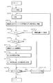
以上の研磨方法をフローチャートを参照して、さらに詳しく説明する。図12は、本発明の第2の実施の形態である研磨方法のステップを示すフローチャートである。この実施の形態の研磨方法では、スタートするとまずウエハ装填工程SP1で1バッチ(例えば5個)のウエハSが(例えば5個の)ウエハ載置部1に載置される。
【0068】
ここで、一般に1バッチとは1回で処理できる1群のウエハをいい、例えば5枚のウエハを1バッチと呼ぶ。また、1ロットとは、同一条件の処理を施す1群のウエハをいい、例えば1ロットは5バッチ分25枚のウエハからなる。1ロットは1カセットともいう。
【0069】
続いて、研磨台3を公転させると共にウエハ載置部1を自転させ、また研磨パッド2を回転させることによりウエハSを研磨する(工程SP2)。研磨が終了すれば、研磨終点近傍のトルクの時間変化率の絶対値X[N・m/min]を求める(工程SP3)。そのためには、例えばトルク測定機構8、18によりトルクを測定し、その測定されたトルクの値を記憶しておき、研磨終了後に、研磨終点より所定時間だけ前から研磨終点までの間の所定の複数時点でのトルクの時間変化率の絶対値を求め、その平均値を上記研磨終点近傍のトルクの時間変化率の絶対値を求め、その平均値を上記研磨終点近傍のトルクの時間変化率の絶対値Xとすればよい。
【0070】
ここで所定の時間は、典型的には、研磨終点近傍において予想されるトルクの時間変化率(トルクの減少あるいは増加勾配)が最も急激な場合(例えば図4、図5中○の場合)のトルクの減少あるいは増加の勾配の開始から勾配の終点(あるいは研磨終点EP)までの時間とする。あるいは、後述のパッドを交換した後の初期のトルクの時間変化率Aの場合の、トルクの勾配の開始から勾配の終点(あるいは研磨終点EP)までの時間としてもよい。
【0071】
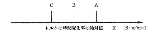
なお、トルクの時間変化率について、図11に示されるような閾値を設定しておく。図11において、Aはパッドを交換した後の初期のトルクの時間変化率であり、Bは軽度の不均一が生じた状態のトルクの時間変化率であり、Cは重度の不均一が生じた状態のトルクの時間変化率である。なお、B=k1・A、C=k2・Aと置くことができる。k1、k2は、トルクの時間変化率比である。
【0072】
ここで、実施例において詳細に説明するが、トルクの時間変化率は、図7、図8に示されるように、ウエハ面内均一性、あるいはウエハ間均一性と相関関係があるので、閾値A、B、Cは、許容均一性をまず設定し、その値から逆に読みとって設定してもよい。
【0073】
例えば図7、図8のデータを与える研磨装置では、パッドを交換した後の初期状態でウエハ面内均一性は約2%であるので、図7によれば、Aは約190[N・m/min]であり、軽度の不均一が生じた状態ではウエハ面内均一性は約4%であるので、Bは約110[N・m/min]であり、重度の不均一が生じた状態ではウエハ面内均一性は約7%であるので、Cは約40[N・m/min]となる。したがって、この場合は、k1は約0.6、k2は約0.2ということになる。
【0074】
図12に戻り、第2の実施の形態の説明を続ける。ステップSP3において求めたトルクの時間変化率の絶対値Xを閾値Cと比較する(ステップSP4)。X<Cのときは、重度の不均一が生じていると判断できるので、研磨パッドやリテーナの極度の劣化(磨耗、消耗等)や、研磨パッドの取り付け不良等が考えられるため、研磨装置を一時停止する(ステップSP5)。
【0075】
図12には不図示であるが、研磨装置を一時停止した後に、作業者による研磨パッドやリテーナの点検、あるいは必要に応じて研磨パッドの交換、リテーナの高さ変更または交換などを行う。
【0076】
ステップSP4において、X≧CのときはさらにXを閾値Bと比較する(ステップSP6)。C≦X<Bのときは、軽度の不均一が生じたと判断できるので、研磨パッドの目立てを行う(ステップSP7)。ここで行う研磨パッドの目立ては、図10に示されるような、研磨装置に備えられているドレッサ(目立て装置)により行うことができる。
【0077】
図10は、研磨装置100を研磨台3の上方から見た平面図である。但し、研磨台とドレッサの関係を示すのに必要な部分以外は図示を省略してある。図10に示されるように、本研磨装置100には、研磨台3の側部に研磨台3と並べて外部ドレッサ30が設けられている。外部ドレッサ30は、表面が研磨パッド2の研磨面2a(図2)の側を向けて設けられたドレッシングホイール32と、ドレッシングホイール32を案内するホイールガイド31とを含んで構成されている。ドレッシングホイール32の上面(研磨面2aに対向する面)にはダイヤモンド砥粒などの高硬度の砥粒が表面に埋め込まれている。このドレッサ30は、必要に応じて自動的に目立てを行うように構成されており、作業者が関与することなく目立てを行い、研磨処理を継続できる。
【0078】
研磨パッド2(の研磨面2a)の目立てが必要と判断されると、研磨パッド2(図10では2点鎖線で表示)は、研磨台3ひいては複数のウエハ載置部1の上方から平行に横に(回転軸23に直角な方向に)移動して、ホイールガイド31の上方に位置する。
【0079】
その状態で、ドレッシングホイール32がホイールガイド31により案内され、ドレッシングホイール32と対向して表面が下方向に向いた研磨パッド2の研磨面2aを舐めるように移動する。即ち、ドレッシングホイール32は研磨パッド2の表面2aに押し当てられ相対的に移動する。このとき、ドレッシングホイール32は自転している。このようにして研磨パッド2は目立てされる。
【0080】
図12に戻り第2の実施の形態の説明を続ける。工程SP6で、B≦Xのときは、問題となるような不均一は生じていないと判断できるので、次の工程SP8で、研磨すべき1ロット分の全てのウエハSが研磨処理されたかを判断し、未処理のウエハSが残っているときは、次に処理すべきウエハSをウエハ載置部1に載置して(ステップSP9)、工程SP2に戻り、既に説明した工程を繰り返す。
【0081】
工程SP8で、全てのウエハが処理されたと判断されると、研磨作業は完了する(エンドとなる)。
【0082】
次に図13を参照して、本発明の第3の実施の形態である研磨方法を説明する。この実施の形態は、ウエハ面内の均一性の悪化の傾向を判定して研磨条件を変更する場合である。
【0083】
図13において、工程SP6までは、実施の形態2の場合と同様であるので重複した説明は省略する。
【0084】
工程SP6で、C≦X<Bのときは、軽度の不均一が生じたと判断できるので、研磨装置に備えられている例えば光学式の膜厚測定器を用いてウエハ表面の複数の測定点における膜厚を測定する(SP11)。この膜厚により研磨量が求められる。
【0085】
この測定結果に基づいて、研磨の均一性悪化の傾向を評価する(SP12)。即ち、典型的には1枚のウエハSにおいてその中央部の研磨が過度なのか、周辺部の研磨が過度なのか、またそのような傾向は全てのウエハに共通なのか、それとも一部の特定のウエハにのみに生じているのか、または1枚のウエハにおいては均一性は悪化していないが複数のウエハ間の均一性が悪化しているのかなどの傾向を判断する。
【0086】
その評価結果に基づいて、即ち不均一な研磨の進行がウエハ面内かウエハ相互間かにより、また不均一さの程度等に応じて、研磨条件の変更(研磨パッド2の回転数の変更、被研磨物Sの回転数の変更、研磨パッド2の研磨面2aを被研磨面Saに押しつける圧力の変更、研磨スラリの流量の変更、研磨パッドの交換、リテーナの調整または交換、研磨パッドの目立ての少なくとも1つ)を適正に行う(SP13)。
【0087】
研磨条件の変更は、研磨条件設定部10、20(図1)により行うことができる。その際は、以上の研磨条件のうちのどの条件が、またどの程度の変更が必要か判断して、研磨台回転駆動機構(被研磨物載置部1の回転駆動機構でもある)4と研磨定盤回転駆動機構7の一方または双方に指令を送り、必要な変更を実行する。このように、以上の処理を自動的に行えるように制御系を設定しておけば、軽度の不均一が生じても作業者が関与する必要がなく、研磨処理を継続できる。
【0088】
次に全てのウエハの研磨処理が完了しているかを判断し(SP8)、完了していればエンドとし、完了していなければ次に処理すべきウエハをウエハ載置台に載置して(SP14)、工程SP2に戻り、既に説明したように研磨を繰り返す。
【0089】
このように、本発明の実施の形態によれば、ウエハ面内およびまたはウエハ間の研磨の均一性の悪化を直ちに修正できるので、研磨不良を最小限に抑え、長期にわたって良好な研磨を実施できる。
【0090】
以上の実施の形態において、研磨の均一性の判断は、トルクやトルク時間変化率を研磨中にトルク測定機構8、18あるいは評価部9、19に組み込まれた不図示の記録部に記録しておいて、1バッチのウエハの研磨が終了してから、その記録に基づいて行う。すなわち、研磨終点より所定の時間だけ前から研磨終点までのトルクの時間変化率の絶対値の平均値を用いて判断している。
【0091】
したがって、研磨条件の設定(研磨パッドの目立ての実施を含む)は、1バッチのウエハの研磨を途中で止めることなく、その1バッチのウエハの研磨が終了してから、いわばバッチ毎に行う。
【0092】
また、研磨の均一性の判断を1バッチのウエハを研磨している最中に行ってもよい。この場合は、(例えば図4、図5から分かるように)研磨開始後しばらくは(研磨終点の近傍以外は)トルクの時間変化率は零に近い値となるので、この零に近い値は均一性の判断から外す必要がある。例えば、図14に示すように閾値Dを加え、図15の第4の実施の形態(第3の実施の形態の変形例)である研磨方法に示すように、トルクの時間変化率の絶対値XがX<Dの場合はそのまま研磨を続ける(SP4a)ようにすればよい。
【0093】
図15において、研磨(SP2)中にトルクの時間変化率の絶対値Xを算出する(SP3a)。そのXを各閾値と比較してその大小を判定する。先ず、工程SP4aでX<Dと判定された場合は、前記のようにそのまま研磨を続けるが、D≦Xと判定された場合は、工程SP4bに進み、さらにXとCの大小を判定する。ここで D≦X<Cと判定された場合は、工程SP5に進み研磨装置を一時停止するのは、図12の場合と同様である。また、工程SP4bでC≦Xと判定された場合は、工程SP6に進む点も、図12の場合と同様である。
【0094】
工程SP6で、B≦Xと判定された場合、研磨終了か否かを判定し(SP8a)、研磨がまだ終了していなければ工程SP2に戻り研磨は継続される。工程SP8aで研磨終了と判定されれば、工程SP8に進み全てのウエハが研磨されたか否かを判定する。以下は図12の場合と同様である。
【0095】
また、予め研磨開始から研磨終了までに要するおおよその時間を求めておき、研磨開始から所定時間経過してから(研磨終点近傍になってから)、図12、図13に示される処理工程に基づいて均一性の判断を行うようにしてもよい。
【0096】
なお、以上実施の形態は、研磨対象の膜質が変化する時点でのトルクの変化を検出し、それに基づいて研磨の均一性の評価を行う場合で説明した。それは、膜質の変化に伴うトルクの変化は一般的には顕著だからである。
【0097】
しかしながら、同じ膜質内での研磨において、凹凸を有する被研磨面が平坦になる過程でのトルクの変化を検出し、それに基づいて研磨の均一性を評価するようにしてもよい。同じ膜質内でのトルク変化は、膜質が変化する場合ほど顕著ではないが、いずれにしても検出可能な変化を生じ得るからである。
【0098】
【実施例】
本発明の研磨方法の実施例について説明する。本実施例で用いた研磨装置は、先に説明した図1に示した装置である。トルクの測定は、研磨定盤回転駆動機構7の電動機に入力される電力を測定して、その電力値と研磨定盤5の回転数とから演算した。
【0099】
研磨に用いたウエハは、シリコンウエハS上にシリコン酸化膜が800nm、その上層にタングステン膜(パターンなし)が600nm成膜されたものである。各研磨回数毎に同一のウエハを5枚載置して研磨を継続した。
【0100】
研磨パッド2は、不織布にポリウレタンを含侵させたものを用いた。研磨スラリは、アルミナ(Al2O3)をKIO3水溶液に懸濁させたものを用いた。
【0101】
研磨定盤5、研磨台3、ウエハ載置部1の回転数は、それぞれ45rpm、7rpm、42rpmとした。
【0102】
図6(a)はウエハの研磨バッチ回数が少ない時点(初期時点)でのトルクの時間変化の測定結果の一例を示す図であり、図6(b)はかなりの回数を処理した時点(後期時点)でのトルクの時間変化の測定結果を示す図である。
【0103】
研磨の終点は、タングステン膜が研磨除去されシリコン酸化膜が露出した時点とし、トルク波形データが所定のトルク値(下限判定設定値)より低下した時点として判定した。図6において研磨終点をEPで示している。
【0104】
なお、実際の半導体製造においては、1つの薄膜層、例えばタングステン膜が完全に研磨除去されて、下層の例えばシリコン酸化膜が露出するような研磨が行われることはほとんどないが、本実施例では実験としてそのような研磨を行った。但し、これは図9に示されるような、配線SX1が研磨面に表れるまで配線間絶縁層SBを研磨除去する場合に模することができる。
【0105】
また、実際の半導体製造においては、EPで示される時点で研磨は終了するのであるが、本実施例では実験として、EP時点以降のトルク変化を検証するために、研磨はEPを越えてしばらく継続し、トルクのデータを採取した。
【0106】
研磨の均一性評価には、研磨終点より所定の時間だけ前、本実施例では0.5min前から研磨終点であるEPで示される点までのトルクの平均勾配の絶対値を用いた。
【0107】
初期時点でのトルクの平均勾配の絶対値は、図6(a)から求められ、190(N・m/min)であった。一方、後期時点での研磨結果の平均勾配の絶対値は、図6(b)から求められ、40(N・m/min)であった。
【0108】
研磨後に膜厚測定器を用いてウエハ各部(面上25点)での研磨厚みを測定し、研磨速度の均一性を評価した。研磨速度のウエハ面内均一性Urは、面内25点での研磨速度の平均値Rmeanと標準偏差σとから、下記の数式(1)に基づいて求めた。
【0109】
ウエハ間(5枚/バッチ)の研磨速度の均一性Srは、各ウエハの平均研磨速度の最大値Rmaxと最小値Rminとから、下記の数式(2)に基づいて求めた。
【0110】
【数1】

【数2】
同様にして、初期時点から後期時点までの中間段階でもトルクの平均勾配の絶対値と研磨の均一性を求めた。
【0113】
その結果、ウエハ面内均一性Ur は、初期時点で2%、中間時点で4%、後期時点で7%であった。また、ウエハ間の均一性Sr は、初期時点で±2%、中間時点で±3.5%、後期時点で±6%であった。この結果を図7と図8に示す。
【0114】
図7に、研磨終点近傍におけるトルクの平均勾配の絶対値と研磨速度のウエハ面内均一性Ur との関係を示す。ここで言う研磨速度とは、膜厚の変化の速さのことであり、膜厚測定器を用いて各ウエハの各部の研磨前後の膜厚を測定し、膜厚の減少分とそのように研磨除去するに要した時間から計算することができる。研磨で除去された膜厚がどれだけ均一かにより、ウエハ面内およびまたはウエハ間の研磨の均一性が評価できる。
【0115】
図7に示されるように、研磨終点近傍におけるトルクの平均勾配の絶対値と研磨速度のウエハ面内均一性Ur とには良好な相関関係が見られた。したがって、薄膜の材質、研磨条件毎に図7に示されるような具体的な相関関係のデータを得ておけば、研磨終点近傍のトルクの平均勾配を測定することにより、ウエハ面内での研磨速度の均一性を評価できる。
【0116】
同様に、図8に研磨終点近傍におけるトルクの平均勾配の絶対値とウエハ間の研磨速度の均一性Sr との関係を示す。この両者にも、ウエハ面内均一性Urと同様に、良好な相関関係が見られた。したがって、やはり薄膜の材質、研磨条件毎に図8に示されるような具体的な相関関係のデータを得ておけば、研磨終点近傍のトルクの平均勾配を測定することにより、複数のウエハ間での研磨速度の均一性をも評価できる。
【0117】
すなわち、研磨終点近傍におけるトルクの平均勾配の絶対値を用いることにより、ウエハ面内均一性Urとウエハ間均一性Srとを重複した研磨の均一性を研磨バッチ毎に判定できることになる。従って、研磨の均一性が所定の許容値内にあるかどうかを、間接的にモニターできることになる。
【0118】
さらに、本実施例においては研磨終点近傍におけるトルクの平均勾配の絶対値が80[N・m/min]以下となったときを一つの基準として、かつ研磨速度が低下傾向にある場合に、研磨条件の一つである研磨パッドまたはリテーナを交換する、または研磨パッドの目立てを実施するというように規定することにより、ウエハ面内およびウエハ間の研磨の均一性の悪化に対処できることを確認した。すなわち、研磨終点近傍のトルクの平均勾配をモニターすることにより、研磨条件を変更する時期の判定ができることを確認した。ただし、本実施例に用いた研磨装置において、判定のための閾値は、80[N・m/min]に限らず、先の実施の形態で説明したように、110[N・m/min]と40[N・m/min]の2つとし、軽度・重度の不均一のように段階的に研磨均一性を判定するようにしてもよい。
【0119】
なお、本実施例では研磨定盤を回転させる回転軸のトルク測定を用いたが、研磨台を回転させる回転軸、複数のウエハ載置部を回転させる各回転軸でトルク計測を行っても研磨の均一性を評価できる。
【0120】
複数のウエハ載置部それぞれの回転軸の研磨終点近傍の回転トルクの平均勾配の絶対値をそれぞれ測定すれば、複数のウエハの各々のウエハ面内均一性Urが評価できると共に、各ウエハ間の均一性Srが評価でき、また研磨台あるいは研磨定盤の一方か両方の研磨終点近傍のトルクの平均勾配の絶対値を測定すれば、ウエハ面内均一性Urとウエハ間均一性Srとを重複した研磨の均一性を研磨バッチ毎に判定できることになる。従って、各ウエハ載置部上のウエハの研磨の均一性が所定の許容値内にあるかどうかを、間接的にモニターできる。
【0121】
【発明の効果】
以上のように本発明によれば、検出されたトルクの時間変化率に基づいて被研磨面Saの研磨均一性を評価するので、被研磨物の膜厚を直接計測しなくても、トルクの時間変化率から研磨均一性を間接的に確実に知ることができる。
【図面の簡単な説明】
【図1】本発明の第1の実施の形態である研磨装置の概略構成図である。
【図2】図1の装置の拡大部分断面図である。
【図3】図2のA−A矢視図である。
【図4】本発明の実施の形態である研磨時のトルクの径時変化(上層薄膜の研磨抵抗が下層薄膜より大の場合)を示す模式図である。
【図5】本発明の実施の形態である研磨時のトルクの径時変化(下層薄膜の研磨抵抗が上層薄膜より大の場合)を示す模式図である。
【図6】トルクの時間変化の一例を示す線図であり、(a)は研磨バッチ回数が少ない時点(初期時点)での、また(b)は研磨バッチ回数がかなり進んだ時点(後期時点)でのトルクの時間変化の一例を示す線図である。
【図7】トルクの研磨終点近傍の平均勾配(絶対値)とウエハ面内均一性との関係を示す線図である。
【図8】トルクの研磨終点近傍の平均勾配(絶対値)とウエハ間均一性との関係を示す線図である。
【図9】ウエハの配線と層間絶縁膜の構造の一例を示す模式的断面図である。
【図10】ドレッサを備える研磨装置の部分平面図である。
【図11】トルクの時間変化率に関する閾値を示す図である。
【図12】本発明の第2の実施の形態である研磨方法のステップを示すフロー図である。
【図13】本発明の第3の実施の形態である研磨方法のステップを示すフロー図である。
【図14】トルクの時間変化率に関する閾値を示す図である。
【図15】本発明の第4の実施の形態である研磨方法のステップを示すフロー図である。
【符号の説明】
1 ウエハ載置部
2 研磨パッド
2a 研磨面
3 研磨台
4 研磨台回転軸駆動機構
5 研磨定盤
7 研磨定盤回転軸駆動機構
8 トルク測定機構
9 評価部
10 研磨条件設定部
11 リテーナ
18 トルク測定機構
18A 測定部
18a〜18e 測定部
19 評価部
19A 評価部
19a〜19e 評価部
20 研磨条件設定部
21 回転軸
22 回転軸
23 回転軸
30 ドレッサ
31 ホイールガイド
32 ドレッシングホイール
100 研磨装置
EP 研磨終点
S ウエハ
Sa 被研磨面
SX1、SX2 配線[0001]
BACKGROUND OF THE INVENTION
The present invention relates to a polishing method and a polishing apparatus used for flattening the surface of a thin film formed on a flat substrate in a manufacturing process of a thin film element such as a semiconductor element, a magnetic element, and an optical element. The present invention relates to a polishing method and a polishing apparatus used for surface flattening of a thin film formed on a surface of a silicon wafer in a manufacturing process.
[0002]
[Prior art]
In recent years, for example, in the manufacturing process of a semiconductor element such as an LSI, multilayer wiring has been used for the purpose of increasing the density of the semiconductor element, and with the miniaturization of the semiconductor element, higher density of wiring formation is required. It is becoming. Therefore, for example, after forming a conductive film to be an interlayer insulating film or wiring on the wafer surface, the unevenness of the surface of these thin films is planarized by chemical mechanical polishing (CMP). It is coming.
[0003]
For polishing the thin film on the wafer surface, a polishing pad attached to a polishing platen is pressed against a wafer placed on a polishing table, and a polishing slurry (abrasive liquid) is supplied while the polishing table and polishing table are supplied. A method of rotating either one or both of the boards is employed. By mounting a plurality of wafers on a polishing table, each wafer is simultaneously polished.
[0004]
Conventionally, when the interlayer insulating film is removed by polishing with a CMP apparatus to flatten the unevenness on the surface of the thin film, if the polishing reaches the base film (lower wiring) and the base film is further polished, Wiring defects occur and affect the characteristics of the manufactured semiconductor.
[0005]
Furthermore, when polishing a plurality of wafers at the same time, the polishing portion is the entire surface of each wafer. Therefore, it is necessary to polish and remove the wafers uniformly within each wafer surface and with the same polishing thickness between each wafer. .
[0006]
Normally, in order to enable such polishing, the initial thickness of the thin film of each wafer is the same, the uniformity of polishing is good within the wafer surface, and the thin film is subjected to polishing conditions with a large selection ratio of the thin film to the base film. Polishing is done. In this case, even if the polishing time is slightly increased so that all the polished surfaces reach the surface of the base film, the selection ratio with respect to the base film is large, so that the amount of polishing of the base film can be suppressed. Here, the selection ratio refers to the ratio of the polishing rate.
[0007]
[Problems to be solved by the invention]
According to the conventional polishing apparatus and polishing method as described above, in general, even if the polishing conditions are constant, fluctuations due to wear of polishing parts such as polishing pads and retainers and disturbances in polishing conditions, and the thin film to be polished Since the state and the like are not constant, the uniformity of polishing within the wafer surface and / or between a plurality of wafers changes.
[0008]
Therefore, even if the polishing conditions satisfying the uniformity of polishing within the wafer surface and the selection ratio with respect to the base film are selected, the polishing may not be performed satisfactorily. Therefore, it is desirable to confirm the uniformity of polishing for each polishing batch. However, it is difficult in commercial production to check the uniformity of polishing within a wafer surface and / or between wafers using a film thickness meter for all polishing.
[0009]
Therefore, an object of the present invention is to provide a polishing method and such a polishing apparatus that can easily evaluate the uniformity of polishing within a wafer surface and the uniformity of polishing between a plurality of wafers. Furthermore, the present invention provides a polishing method and a polishing apparatus capable of performing good polishing over a long period of time by immediately determining whether the uniformity of polishing within a wafer surface or the deterioration of polishing uniformity between a plurality of wafers. It is aimed.
[0010]
[Means for Solving the Problems]
In order to achieve the above object, the polishing method according to the first aspect of the present invention comprises:, CoveredPolishingThingPolishedOn the facePolishing padDoPressing and polishingThingsAnd the polishing padDeRotate at least one of the objects to be polishedThingsA polishing method for polishingThe abovePolishing padDoRotating torque to rotate and the object to be polishedThingsDetect the time change rate of at least one of the rotating torques to rotate, InspectionBased on the time change rate of the output torqueSaidPolishedPlaneThe polishing uniformity is evaluated.In the polishing method according to the second aspect of the present invention, the object to be polished is plural.. For example, referring to FIG. 2, the rotational torque for rotating the
[0011]
With this configuration, the polishing uniformity of the surface to be polished Sa is evaluated based on the detected time change rate of the torque, so that the polishing uniformity can be obtained without directly measuring the film thickness at a plurality of measurement points of the object to be polished. Can be indirectly and reliably known from the time change rate of the torque.
[0012]
In addition,As shown in FIGS. 1 to 3, the
[0013]
If comprised in this way, based on the time change rate of the torque of the at least 1 rotating shaft of each rotating
[0014]
In the above polishing method, a polishing slurry may be supplied between the workpiece S and the
[0015]
In the above polishing method, as described in
[0016]
At this time, since the polishing conditions are set based on the evaluated polishing uniformity, when it is found that the progress of polishing within the wafer surface or between the wafers is not uniform, the polishing conditions can be changed to correct it.
[0017]
As described in
[0018]
In order to achieve the above object, a polishing apparatus according to the invention of
[0019]
If comprised in this way, when using especially the torque of the
[0020]
In the above polishing apparatus, the claim8As described in, ReviewSet polishing conditions based on rated polishing uniformityMeansYou may prepare.
[0021]
With this configuration, the polishing conditions can be set so that the polishing condition setting unit 10 (20) corrects the polishing failure based on the polishing uniformity evaluated by the evaluation unit 9 (19).
[0022]
DETAILED DESCRIPTION OF THE INVENTION
Embodiments of the present invention will be described below with reference to the drawings. In addition, in each figure, the same code | symbol is attached | subjected to the mutually same or equivalent member, and the overlapping description is abbreviate | omitted.
[0023]
The present inventors paid attention to the torque change during polishing, which is used as one method for detecting the end point of polishing, and further completed the present invention based on the following knowledge by using the time change rate of the torque. I let you.
[0024]
In a polishing apparatus having a structure in which a plurality of wafers to be polished are simultaneously polished on a polishing table, the interlayer insulating film of the wafer to be polished generally has a structure of two or more layers. Thin films usually have different polishing resistances. FIG. 9 is a sectional view showing an example of the structure of the interlayer insulating film.
[0025]
In the interlayer insulating film shown in FIG. 9, a wiring SX1 is formed on a wafer substrate SA such as silicon, and a space between the wirings is filled with an inter-wiring insulating film SB. In forming these, first, the wiring SX1 is formed on the wafer substrate SA, the inter-wiring insulating film SB is deposited so as to cover the upper surface, and then the inter-wiring insulating film SB has the same height as the wiring SX1. By polishing to a height, the upper portion of the wiring SX1 is exposed from the inter-wiring insulating film SB so as to be a flat surface as a whole.
[0026]
A first interlayer insulating film SC is deposited on the flat surface, its upper surface is polished to become a flat surface, a second wiring SX2 is formed on the flat surface, and the wiring is formed so as to cover it. The insulating film SD is deposited, and then the inter-wiring insulating film SD is polished and removed to the same height as the wiring SX2, and the upper portion of the wiring SX2 is exposed from the inter-wiring insulating film SD, and becomes a flat surface as a whole. It is processed as follows. In FIG. 9, the inter-wiring insulating film SD has not been polished and removed, and a portion that is polished and becomes a flat surface is indicated by a broken line. That is, it is the height at which the upper portion of the wiring SX2 is exposed.
[0027]
In the detection of the polishing end point of the multilayer insulating film structure such as the upper surfaces of the wiring SX1 and the inter-wiring insulating film SB shown in FIG. 9, the polishing torque indicates the difference in polishing resistance when the upper layer is removed by polishing and the lower layer appears. Detection is made using the decrease or increase, and the polishing end point is determined.
[0028]
Here, the polishing torque changes substantially in proportion to the appearance area of the lower thin film when the upper thin film is removed and the lower thin film appears. Accordingly, when the polishing is progressing uniformly within the wafer surface and between the wafers, the thin film to be polished is removed almost simultaneously in each part of the wafer surface and between the plurality of wafers, and the underlying film is exposed. As a result, since the area of the base film increases rapidly, the torque decrease rate or increase rate near the polishing end point, that is, the torque change rate with time increases.
[0029]
On the other hand, when the polishing is not progressing uniformly within one wafer surface or between a plurality of wafers, the time when the thin film to be polished is removed and the underlying film is exposed in each part of the wafer surface and between the wafers is shifted. As a result, the increase in the area of the base film becomes gradual, and the time change rate of the torque near the polishing end point becomes small.
[0030]
With reference to the schematic diagram of the torque change in FIG. 4, the torque change with the progress of polishing will be described in the case where the polishing resistance of the upper thin film is larger than that of the lower thin film.
[0031]
When polishing within the wafer surface is progressing uniformly (in the case of ◯ in the figure), the decreasing gradient with respect to time of the torque in the vicinity of the polishing end point (EP in the figure), that is, the time change rate of the torque is abrupt. On the other hand, when the polishing in the wafer surface is progressing non-uniformly (in the case of Δ and □ in the figure), the torque decreasing gradient near the polishing end point becomes gentle as the polishing uniformity deteriorates. Become.
[0032]
When a diagram as shown in FIG. 4 is created for each of a plurality of wafers, if the in-plane polishing of each of the plurality of wafers is uniform and the polishing between the plurality of wafers progresses unevenly, Although the torque decreasing gradient is steep, the time position of the polishing end point EP deviates for each diagram.
[0033]
In addition, when a diagram showing the overall polishing uniformity of a plurality of wafers is created (by measuring the torque of the rotating shaft of the polishing table or the rotating shaft of the polishing surface plate), the in-plane polishing of each of the plurality of wafers is performed. If the uniformity is poor or the polishing uniformity between the wafers is poor, the torque decreasing gradient becomes gentle. In this case, if the in-plane polishing uniformity of each of the plurality of wafers is good and the polishing uniformity between the wafers is also good, the torque decreasing gradient becomes steep.
[0034]
FIG. 5 shows a schematic diagram of a change in torque as the polishing progresses when the upper layer has a lower polishing resistance than the lower layer.
[0035]
When polishing within the wafer surface is progressing uniformly (in the case of ◯ in the figure), the torque increasing gradient near the polishing end point (EP in the figure), that is, the time change rate of the torque is abrupt. On the other hand, when the polishing in the wafer surface is progressing non-uniformly (in the case of Δ and □ in the figure), the increasing gradient of torque near the polishing end point becomes gentle as the polishing uniformity deteriorates. Become.
[0036]
The knowledge when the diagram as shown in FIG. 5 is created for each of the plurality of wafers is the same as in the case of FIG.
[0037]
The uniformity of polishing within a surface to be polished of one wafer and / or between a plurality of wafers can be quantified by the magnitude of the time change rate (first-order differential value with respect to time) of this polishing torque. Can be evaluated. Then, it can be easily determined whether the polishing has been performed satisfactorily.
[0038]
Embodiments of the present invention will be described below with reference to the drawings. FIG. 1 is a perspective view of a polishing apparatus using CMP according to a first embodiment of the present invention, FIG. 2 is an enlarged sectional view of a part of the polishing apparatus in FIG. 1, and FIG. It is a top view (AA arrow line view of FIG. 2) of the grinding | polishing stand which mounts the to-be-polished object mounting part of the apparatus of FIG.
[0039]
1 and 2, a disk-shaped
[0040]
A polishing table 3 is provided below the polishing
[0041]
In addition, on the polishing table 3 side of the polishing table 3, there are a plurality of circular wafer mounting portions 1 (5 in the present embodiment) that are objects to be polished so as to face the
[0042]
Below the
[0043]
The rotating
[0044]
In such a configuration, the polishing table 3 is rotated by the polishing table
[0045]
The rotation axis of the
[0046]
A polishing
[0047]
A
[0048]
The
[0049]
As a configuration of the
[0050]
The detection of the rotational torque of the
[0051]
The
[0052]
The
[0053]
The configuration of the
[0054]
The
[0055]
If the torque is measured with respect to the
[0056]
On the other hand, if the torque is measured for each
[0057]
As described above, the
[0058]
Further, in the
[0059]
Further, the
[0060]
In the polishing method according to the embodiment of the present invention, which can be performed using the polishing apparatus as described above, the object to be polished S placed on the plurality of objects to be polished
[0061]
As described above, according to the embodiment of the present invention, even in a polishing apparatus, in particular, a CMP apparatus that performs high-precision flattening with a small amount of polishing, polishing of a wafer, which is an object to be polished, can be performed uniformly through the torque of the rotating shaft. Sexual status can be detected quantitatively. As a result, the quality of the product can be determined simultaneously with the polishing, and the product inspection mechanism can be simplified.
[0062]
Also, based on the evaluation results of the uniformity of polishing within and between wafers, the polishing conditions for the next and subsequent times will be corrected, and a more detailed evaluation will be performed using a film thickness meter for polishing uniformity. Can do.
[0063]
For example, when it is judged that the polishing uniformity is poor, the polishing pad is sharpened, the polishing pad is replaced, the height of the retainer is changed or replaced. Adjustment such as a change in the height of the retainer can be performed by, for example, inserting a shim between the retainer and the
[0064]
Here, the sharpening of the polishing pad refers to, for example, a polishing pad by moving a dresser (shaping machine) embedded with high-hardness abrasive grains such as diamond abrasive grains against the surface of the polishing pad and moving it relatively. The surface is ground to sharpen the polishing pad surface.
[0065]
When the polishing of the object to be polished is repeated, clogging or polishing slurry may enter the fine holes on the surface of the polishing pad and cause clogging. When this clogging occurs in a part of the polishing pad, it leads to deterioration of polishing uniformity. Therefore, the deterioration of uniformity can be corrected by sharpening the polishing pad.
[0066]
Also, when the uniformity is judged to be poor, the film thickness is measured at a plurality of measurement points on the wafer surface using an optical film thickness measuring instrument, and the uniformity tendency (the central portion of the wafer is excessively shaved) Or whether the deterioration is in the periphery or whether the deterioration of uniformity is within the wafer surface or between the wafers). Based on the evaluation results, in addition to the above polishing conditions, The number of rotations of the rotating shaft, the polishing pressure that presses the polishing pad against the object to be polished, the flow rate of the polishing slurry, and the like may be changed to appropriate values. In this case, it is not necessary to measure the polishing amount with a film thickness measuring device every time, so that it is suitable for commercial production.
[0067]
The above polishing method will be described in more detail with reference to a flowchart. FIG. 12 is a flowchart showing steps of a polishing method according to the second embodiment of the present invention. In the polishing method of this embodiment, when started, first, one batch (for example, five) of wafers S is mounted on the (for example, five)
[0068]
Here, one batch generally refers to a group of wafers that can be processed at one time. For example, five wafers are referred to as one batch. One lot refers to a group of wafers that are processed under the same conditions. For example, one lot includes 25 wafers for 5 batches. One lot is also called one cassette.
[0069]
Subsequently, the wafer S is polished by rotating the polishing table 3 and rotating the
[0070]
Here, the predetermined time is typically when the rate of change with time of torque (decrease or increase in torque) expected in the vicinity of the polishing end point is the steepest (for example, in the case of ○ in FIGS. 4 and 5). The time from the start of the gradient of torque decrease or increase to the end point of the gradient (or polishing end point EP). Alternatively, it may be the time from the start of the torque gradient to the end point of the gradient (or the polishing end point EP) in the case of the time change rate A of the initial torque after replacing the pads described later.
[0071]
Note that a threshold as shown in FIG. 11 is set for the time change rate of the torque. In FIG. 11, A is the time change rate of the initial torque after replacing the pad, B is the time change rate of the torque in a state where a slight non-uniformity occurs, and C is a severe non-uniformity. It is the time change rate of the torque of the state. B = k1 · A and C = k2 · A can be set. k1 and k2 are torque change ratios over time.
[0072]
Here, as will be described in detail in the embodiment, the time change rate of the torque has a correlation with the uniformity within the wafer surface or between the wafers as shown in FIGS. , B, and C may be set by first setting the allowable uniformity and then reading back from the value.
[0073]
For example, in the polishing apparatus that provides the data shown in FIGS. 7 and 8, the uniformity within the wafer surface is about 2% in the initial state after the pad is replaced. Therefore, according to FIG. 7, A is about 190 [N · m / Min], and in the state where slight non-uniformity occurs, the wafer in-plane uniformity is about 4%. Therefore, B is about 110 [N · m / min], and severe non-uniformity occurs. Then, since the wafer in-plane uniformity is about 7%, C is about 40 [N · m / min]. Therefore, in this case, k1 is about 0.6 and k2 is about 0.2.
[0074]
Returning to FIG. 12, the description of the second embodiment will be continued. The absolute value X of the torque change rate obtained in step SP3 is compared with a threshold value C (step SP4). When X <C, it can be determined that severe non-uniformity has occurred. Therefore, the polishing pad or retainer may be extremely deteriorated (wear, wear, etc.), or the polishing pad may be poorly attached. Temporarily stop (step SP5).
[0075]
Although not shown in FIG. 12, after the polishing apparatus is temporarily stopped, the operator inspects the polishing pad and the retainer, or replaces the polishing pad and changes or replaces the height of the retainer as necessary.
[0076]
In step SP4, when X ≧ C, X is further compared with the threshold value B (step SP6). When C ≦ X <B, it can be determined that a slight non-uniformity has occurred, so the polishing pad is sharpened (step SP7). The polishing pad sharpening performed here can be performed by a dresser (shaping device) provided in the polishing apparatus as shown in FIG.
[0077]
FIG. 10 is a plan view of the
[0078]
When it is determined that the polishing pad 2 (the polishing
[0079]
In this state, the
[0080]
Returning to FIG. 12, the description of the second embodiment is continued. In step SP6, when B ≦ X, it can be determined that non-uniformity that causes a problem does not occur. Therefore, in the next step SP8, whether all the wafers S for one lot to be polished have been polished. If the unprocessed wafer S remains, the wafer S to be processed next is mounted on the wafer mounting unit 1 (step SP9), and the process returns to the process SP2 to repeat the process already described.
[0081]
If it is determined in step SP8 that all the wafers have been processed, the polishing operation is completed (end).
[0082]
Next, a polishing method according to a third embodiment of the present invention will be described with reference to FIG. In this embodiment, the polishing condition is changed by determining the tendency of the uniformity in the wafer surface to deteriorate.
[0083]
In FIG. 13, the process up to step SP6 is the same as that in the second embodiment, and a duplicate description is omitted.
[0084]
In step SP6, when C ≦ X <B, it can be determined that a slight non-uniformity has occurred. Therefore, for example, at a plurality of measurement points on the wafer surface using an optical film thickness measuring instrument provided in the polishing apparatus. The film thickness is measured (SP11). The polishing amount is determined by this film thickness.
[0085]
Based on this measurement result, the tendency of deterioration of polishing uniformity is evaluated (SP12). That is, typically, in a single wafer S, whether the polishing of the central portion is excessive or the peripheral portion is excessively polished, and whether such a tendency is common to all wafers, or a part of the specification. The tendency is determined whether it occurs only in a single wafer, or whether the uniformity among a plurality of wafers is deteriorated although the uniformity is not deteriorated in one wafer.
[0086]
Based on the evaluation result, that is, depending on whether the progress of non-uniform polishing is within the wafer surface or between wafers, and depending on the degree of non-uniformity, etc., the change of polishing conditions (change in the number of rotations of the
[0087]
The polishing condition can be changed by the polishing
[0088]
Next, it is determined whether or not the polishing process has been completed for all the wafers (SP8). If completed, the process is ended. If not completed, the wafer to be processed next is mounted on the wafer mounting table (SP14). ), Returning to step SP2, and repeating the polishing as already described.
[0089]
As described above, according to the embodiment of the present invention, the deterioration of the uniformity of the polishing within the wafer surface and / or between the wafers can be corrected immediately, so that polishing defects can be minimized and good polishing can be performed over a long period of time. .
[0090]
In the above embodiment, the determination of the uniformity of polishing is performed by recording the torque and the rate of change in torque time in the
[0091]
Therefore, the setting of the polishing conditions (including the sharpening of the polishing pad) is performed for each batch after the polishing of the batch of wafers is completed without stopping the polishing of the batch of wafers halfway.
[0092]
Further, the uniformity of the polishing may be determined while polishing one batch of wafers. In this case, since the rate of change with time of torque becomes a value close to zero for a while after the start of polishing (except in the vicinity of the polishing end point) (for example, as can be seen from FIGS. 4 and 5), the value close to zero is uniform. It is necessary to exclude from the judgment of sex. For example, as shown in FIG. 14, the threshold value D is added, and the absolute value of the time change rate of the torque as shown in the polishing method of the fourth embodiment (modified example of the third embodiment) in FIG. If X is X <D, polishing may be continued as it is (SP4a).
[0093]
In FIG. 15, the absolute value X of the time change rate of torque is calculated during polishing (SP2) (SP3a). The X is compared with each threshold value to determine the magnitude. First, if it is determined in step SP4a that X <D, the polishing is continued as described above. However, if it is determined that D ≦ X, the process proceeds to step SP4b, and X and C are further determined. Here, when it is determined that D ≦ X <C, the process proceeds to step SP5 and the polishing apparatus is temporarily stopped as in the case of FIG. Further, when it is determined in step SP4b that C ≦ X, the process proceeds to step SP6 as in the case of FIG.
[0094]
If it is determined in step SP6 that B ≦ X, it is determined whether or not the polishing is completed (SP8a). If the polishing is not yet completed, the process returns to step SP2 and the polishing is continued. If it is determined in step SP8a that the polishing is completed, the process proceeds to step SP8 to determine whether or not all the wafers have been polished. The following is the same as in FIG.
[0095]
Further, an approximate time required from the start of polishing to the end of polishing is obtained in advance, and after a predetermined time has elapsed from the start of polishing (after the vicinity of the polishing end point), the processing steps shown in FIGS. The uniformity may be determined.
[0096]
The above embodiment has been described in the case where a change in torque at the time when the film quality to be polished changes is detected and the uniformity of polishing is evaluated based on the change. This is because a change in torque accompanying a change in film quality is generally remarkable.
[0097]
However, in polishing within the same film quality, it is also possible to detect a change in torque in the process of flattening the surface to be polished having unevenness, and to evaluate polishing uniformity based on the change. This is because a torque change within the same film quality is not as significant as when the film quality changes, but in any case a detectable change can occur.
[0098]
【Example】
Examples of the polishing method of the present invention will be described. The polishing apparatus used in this example is the apparatus shown in FIG. 1 described above. The torque was measured by measuring the electric power input to the electric motor of the polishing surface plate rotation drive mechanism 7 and calculating from the electric power value and the rotation speed of the polishing
[0099]
The wafer used for polishing is obtained by forming a silicon oxide film on the silicon wafer S with a thickness of 800 nm and an upper layer with a tungsten film (no pattern) having a thickness of 600 nm. Polishing was continued by placing five identical wafers for each polishing.
[0100]
As the
[0101]
The rotation speeds of the polishing
[0102]
FIG. 6A is a diagram illustrating an example of a measurement result of a change in torque over time when the number of wafer polishing batches is small (initial time), and FIG. It is a figure which shows the measurement result of the time change of the torque at a time.
[0103]
The end point of polishing was determined as the time when the tungsten film was removed by polishing and the silicon oxide film was exposed, and the time when the torque waveform data decreased below a predetermined torque value (lower limit determination set value). In FIG. 6, the polishing end point is indicated by EP.
[0104]
In actual semiconductor manufacturing, one thin film layer, such as a tungsten film, is completely polished and removed so that the underlying silicon oxide film, for example, is barely exposed. Such polishing was performed as an experiment. However, this can be simulated when the inter-wiring insulating layer SB is removed by polishing until the wiring SX1 appears on the polished surface as shown in FIG.
[0105]
In actual semiconductor manufacturing, polishing is completed at the point indicated by EP, but in this example, as an experiment, polishing is continued for a while beyond the EP in order to verify the torque change after the point of EP. Torque data was collected.
[0106]
For the evaluation of polishing uniformity, the absolute value of the average gradient of torque from a point before the polishing end point by a predetermined time, in this example, from 0.5 min before to the point indicated by EP as the polishing end point was used.
[0107]
The absolute value of the average torque gradient at the initial time point was found from FIG. 6A and was 190 (N · m / min). On the other hand, the absolute value of the average gradient of the polishing results at the later stage was obtained from FIG. 6B and was 40 (N · m / min).
[0108]
After polishing, the thickness of each portion of the wafer (25 points on the surface) was measured using a film thickness measuring instrument to evaluate the uniformity of the polishing rate. The wafer in-plane uniformity Ur of the polishing rate was obtained from the average value Rmean and standard deviation σ of the polishing rate at 25 points in the surface based on the following formula (1).
[0109]
Uniformity Sr of polishing rate between wafers (5 wafers / batch) was obtained from the maximum value Rmax and the minimum value Rmin of the average polishing rate of each wafer based on the following formula (2).
[0110]
[Expression 1]
[Expression 2]
Similarly, the absolute value of the average torque gradient and the uniformity of polishing were also obtained in the intermediate stage from the initial time point to the late time point.
[0113]
As a result, the wafer in-plane uniformity Ur was 2% at the initial time point, 4% at the intermediate time point, and 7% at the late time point. The uniformity Sr between wafers was ± 2% at the initial time point, ± 3.5% at the intermediate time point, and ± 6% at the late time point. The results are shown in FIGS.
[0114]
FIG. 7 shows the relationship between the absolute value of the average torque gradient near the polishing end point and the wafer surface uniformity Ur of the polishing rate. The polishing rate here means the rate of change of the film thickness. The film thickness measuring instrument is used to measure the film thickness of each part of each wafer before and after polishing, and the decrease in film thickness and so on. It can be calculated from the time required for polishing removal. The uniformity of polishing within the wafer surface and / or between the wafers can be evaluated according to how uniform the film thickness removed by polishing is.
[0115]
As shown in FIG. 7, a good correlation was found between the absolute value of the average gradient of the torque near the polishing end point and the wafer in-plane uniformity Ur of the polishing rate. Therefore, if specific correlation data as shown in FIG. 7 is obtained for each material of the thin film and polishing conditions, the average gradient of the torque in the vicinity of the polishing end point is measured, so that polishing within the wafer surface is performed. Speed uniformity can be evaluated.
[0116]
Similarly, FIG. 8 shows the relationship between the absolute value of the average torque gradient near the polishing end point and the uniformity Sr of the polishing rate between the wafers. A good correlation was observed in both cases as well as the wafer in-plane uniformity Ur. Therefore, if the data of the specific correlation as shown in FIG. 8 is obtained for each material of the thin film and the polishing conditions, the average gradient of the torque in the vicinity of the polishing end point can be measured, and a plurality of wafers can be measured. The uniformity of the polishing rate can also be evaluated.
[0117]
That is, by using the absolute value of the average gradient of the torque in the vicinity of the polishing end point, it is possible to determine for each polishing batch the polishing uniformity that overlaps the wafer in-plane uniformity Ur and the inter-wafer uniformity Sr. Therefore, it is possible to indirectly monitor whether the polishing uniformity is within a predetermined tolerance.
[0118]
Further, in this example, when the absolute value of the average torque gradient in the vicinity of the polishing end point is 80 [N · m / min] or less as one criterion and when the polishing rate tends to decrease, polishing is performed. It was confirmed that the deterioration of the uniformity of polishing within the wafer surface and between the wafers can be dealt with by changing the polishing pad or the retainer, which is one of the conditions, or performing the sharpening of the polishing pad. That is, it was confirmed that the timing for changing the polishing conditions could be determined by monitoring the average torque gradient near the polishing end point. However, in the polishing apparatus used in this example, the threshold value for determination is not limited to 80 [N · m / min], but as described in the previous embodiment, 110 [N · m / min]. And 40 [N · m / min], and polishing uniformity may be judged step by step such as mild and severe non-uniformity.
[0119]
In this embodiment, torque measurement of the rotating shaft that rotates the polishing surface plate is used. However, even if torque measurement is performed on the rotating shaft that rotates the polishing table and each rotating shaft that rotates the plurality of wafer mounting portions, the polishing is performed. Can be evaluated.
[0120]
By measuring the absolute value of the average gradient of the rotational torque in the vicinity of the polishing end point of the rotation axis of each of the plurality of wafer mounting portions, the wafer in-plane uniformity Ur of each of the plurality of wafers can be evaluated, and Uniformity Sr can be evaluated, and if the absolute value of the average gradient of torque in the vicinity of the polishing end point on either the polishing table or the polishing surface plate is measured, the in-wafer uniformity Ur and the inter-wafer uniformity Sr overlap. The uniformity of the polished polishing can be determined for each polishing batch. Accordingly, it is possible to indirectly monitor whether or not the polishing uniformity of the wafer on each wafer mounting portion is within a predetermined allowable value.
[0121]
【The invention's effect】
As described above, according to the present invention, the polishing uniformity of the surface to be polished Sa is evaluated based on the detected time change rate of the torque, so that the torque can be measured without directly measuring the film thickness of the object to be polished. The polishing uniformity can be indirectly and reliably known from the time change rate.
[Brief description of the drawings]
FIG. 1 is a schematic configuration diagram of a polishing apparatus according to a first embodiment of the present invention.
FIG. 2 is an enlarged partial cross-sectional view of the apparatus of FIG.
FIG. 3 is a view taken along arrow AA in FIG. 2;
FIG. 4 is a schematic diagram showing a change in torque with time during polishing (when the polishing resistance of the upper thin film is larger than that of the lower thin film) according to the embodiment of the present invention.
FIG. 5 is a schematic diagram showing a change in torque with time during polishing (when the polishing resistance of the lower layer thin film is larger than that of the upper layer thin film) according to the embodiment of the present invention.
FIGS. 6A and 6B are diagrams showing an example of a temporal change in torque, where FIG. 6A is a time when the number of polishing batches is small (initial time), and FIG. 6B is a time when the number of polishing batches is considerably advanced (late time). It is a diagram which shows an example of the time change of the torque in FIG.
FIG. 7 is a diagram showing a relationship between an average gradient (absolute value) in the vicinity of a polishing polishing end point and uniformity within a wafer surface.
FIG. 8 is a diagram showing a relationship between an average gradient (absolute value) in the vicinity of a polishing polishing end point and uniformity between wafers.
FIG. 9 is a schematic cross-sectional view showing an example of a structure of a wafer wiring and an interlayer insulating film.
FIG. 10 is a partial plan view of a polishing apparatus including a dresser.
FIG. 11 is a diagram showing a threshold concerning a time change rate of torque.
FIG. 12 is a flowchart showing steps of a polishing method according to a second embodiment of the present invention.
FIG. 13 is a flowchart showing steps of a polishing method according to a third embodiment of the present invention.
FIG. 14 is a diagram showing a threshold concerning a time change rate of torque.
FIG. 15 is a flowchart showing steps of a polishing method according to a fourth embodiment of the present invention.
[Explanation of symbols]
1 Wafer mounting part
2 Polishing pad
2a Polished surface
3 Polishing table
4 Polishing table rotating shaft drive mechanism
5 Polishing surface plate
7 Polishing surface plate rotary shaft drive mechanism
8 Torque measurement mechanism
9 Evaluation Department
10 Polishing condition setting section
11 Retainer
18 Torque measurement mechanism
18A measurement unit
18a-18e measuring unit
19 Evaluation Department
19A Evaluation Department
19a-19e Evaluation Department
20 Polishing condition setting section
21 Rotating shaft
22 Rotating shaft
23 Rotating shaft
30 Dresser
31 Wheel guide
32 Dressing wheel
100 polishing equipment
EP polishing end point
S wafer
Sa Surface to be polished
SX1, SX2 wiring
Claims (8)
前記研磨パッドを回転させる回転トルクおよび前記被研磨物を回転させる回転トルクの少なくとも一方の回転トルクの時間変化率を検出し、
検出された回転トルクの時間変化率に基づいて前記被研磨面の研磨均一性を評価することを特徴とする研磨方法。A polishing method in which a polishing pad is pressed against a surface to be polished of an object to be polished, and the object to be polished is polished by rotating at least one of the object to be polished and the polishing pad ,
Detecting a time change rate of a rotational torque of at least one of a rotational torque for rotating the polishing pad and a rotational torque for rotating the workpiece ;
Migaku Ken how to and evaluating the polishing uniformity of the polished surface based on the time rate of change of the test out rotational torque.
前記研磨台に取り付けられた被研磨物に押し当てられて前記被研磨物を研磨する研磨パッドと、
前記研磨パッドを被着して、他の回転軸回りに回転する研磨定盤と、
各回転軸のうち少なくとも1つの回転軸のトルクの時間変化率を検出するトルク時間変化率検出部と、
前記トルク時間変化率検出部で検出されたトルクの時間変化率に基づいて前記被研磨面の研磨均一性を評価する評価部と
を備えることを特徴とする研磨装置。And that Ken Migakudai be rotated to an axis of rotation and the object to be polished is attached,
A polishing pad that is pressed against an object to be polished attached to the polishing table and polishes the object to be polished ;
A polishing platen that is attached to the polishing pad and rotates about another rotation axis ;
And the torque time rate of change detector for detecting a time rate of change of torque of at least one axis of rotation of the respective rotary shaft,
Be that Migaku Ken apparatus characterized by comprising an evaluation unit for evaluating the polishing uniformity of the polished surface on the basis of the time change rate of the detected torque by the torque time rate of change detection section.
前記研磨パッドを回転させる回転トルクおよび前記被研磨物を回転させる回転トルクの少なくとも一方の回転トルクの時間変化率を検出する手段と、
検出された回転トルクの時間変化率に基づいて前記被研磨面の研磨均一性を評価する手段と
を備えることを特徴とする研磨装置。 A polishing apparatus that presses a polishing pad against a surface to be polished and rotates at least one of the object to be polished and the polishing pad to polish the object to be polished,
Means for detecting a time change rate of at least one of rotational torque for rotating the polishing pad and rotational torque for rotating the workpiece;
Means for evaluating the polishing uniformity of the surface to be polished based on the rate of time change of the detected rotational torque;
Migaku Ken apparatus you comprising: a.
Priority Applications (1)
| Application Number | Priority Date | Filing Date | Title |
|---|---|---|---|
| JP06434498A JP4067164B2 (en) | 1998-02-27 | 1998-02-27 | Polishing method and polishing apparatus |
Applications Claiming Priority (1)
| Application Number | Priority Date | Filing Date | Title |
|---|---|---|---|
| JP06434498A JP4067164B2 (en) | 1998-02-27 | 1998-02-27 | Polishing method and polishing apparatus |
Publications (2)
| Publication Number | Publication Date |
|---|---|
| JPH11251272A JPH11251272A (en) | 1999-09-17 |
| JP4067164B2 true JP4067164B2 (en) | 2008-03-26 |
Family
ID=13255537
Family Applications (1)
| Application Number | Title | Priority Date | Filing Date |
|---|---|---|---|
| JP06434498A Expired - Fee Related JP4067164B2 (en) | 1998-02-27 | 1998-02-27 | Polishing method and polishing apparatus |
Country Status (1)
| Country | Link |
|---|---|
| JP (1) | JP4067164B2 (en) |
Families Citing this family (9)
| Publication number | Priority date | Publication date | Assignee | Title |
|---|---|---|---|---|
| JP2001138219A (en) * | 1999-11-19 | 2001-05-22 | Disco Abrasive Syst Ltd | Grinding apparatus |
| JP4827292B2 (en) * | 2000-11-01 | 2011-11-30 | アプライド マテリアルズ インコーポレイテッド | Polishing equipment |
| JP3456642B2 (en) * | 2000-11-10 | 2003-10-14 | 茂徳科技股▲ふん▼有限公司 | A method for determining the thickness of a film to be planarized in chemical mechanical polishing |
| JP2003318140A (en) * | 2002-04-26 | 2003-11-07 | Applied Materials Inc | Polishing method and device thereof |
| JP4664617B2 (en) * | 2004-04-27 | 2011-04-06 | 富士通セミコンダクター株式会社 | Polishing apparatus and method |
| US20100099342A1 (en) * | 2008-10-21 | 2010-04-22 | Applied Materials, Inc. | Pad conditioner auto disk change |
| SG10202111787PA (en) * | 2016-10-18 | 2021-11-29 | Ebara Corp | Local polisher, method of a local polisher and program |
| JP6817778B2 (en) * | 2016-10-18 | 2021-01-20 | 株式会社荏原製作所 | Local polishing equipment, local polishing methods and programs |
| KR102525737B1 (en) * | 2016-11-16 | 2023-04-26 | 주식회사 케이씨텍 | Chemical mechanical polishing apparatus and control method thereof |
-
1998
- 1998-02-27 JP JP06434498A patent/JP4067164B2/en not_active Expired - Fee Related
Also Published As
| Publication number | Publication date |
|---|---|
| JPH11251272A (en) | 1999-09-17 |
Similar Documents
| Publication | Publication Date | Title |
|---|---|---|
| US9211631B2 (en) | Grinding wheel truing tool and manufacturing method thereof, and truing apparatus, method for manufacturing grinding wheel and wafer edge grinding apparatus using the same | |
| US6517414B1 (en) | Method and apparatus for controlling a pad conditioning process of a chemical-mechanical polishing apparatus | |
| US6783436B1 (en) | Polishing pad with optimized grooves and method of forming same | |
| KR100818683B1 (en) | Mirror chamfered wafer, mirror chamfering polishing cloth, and mirror chamfering polishing machine and method | |
| WO2018083931A1 (en) | Double side polishing method for semiconductor wafer | |
| JP2004142083A (en) | Wafer polishing device and wafer polishing method | |
| JPH09270401A (en) | Polishing method of semiconductor wafer | |
| WO2000067950A1 (en) | Method and device for simultaneously grinding double surfaces, and method and device for simultaneously lapping double surfaces | |
| TWI774805B (en) | Wafer Processing Method | |
| JP4067164B2 (en) | Polishing method and polishing apparatus | |
| US9908213B2 (en) | Method of CMP pad conditioning | |
| CN113941954B (en) | Large-area quartz wafer grinding device and grinding method thereof | |
| JP2023088052A (en) | Manufacturing apparatus and manufacturing method for semiconducting crystal wafer | |
| JP2003151934A (en) | Cmp system and method of adjusting polishing pad for cmp | |
| JP2002066905A (en) | Manufacturing method for semiconductor device and device therefor | |
| JP3706306B2 (en) | Module control platen manufacturing system and method | |
| CN208663464U (en) | Chemical mechanical polishing device | |
| KR100789842B1 (en) | Apparatus for mesuring the pad surface profile, and method of revising the pad surface profile taking use of it, and chemical mechanical polishing equipment taking use of it | |
| JP3045236B1 (en) | Wafer polishing apparatus with polishing cloth conditioner | |
| JPH06315850A (en) | Detecting device for polishing end point | |
| TW200527525A (en) | Method for CMP removal rate compensation | |
| JPH10315124A (en) | Polishing method and polishing device | |
| JP3019849B1 (en) | Chemical mechanical polishing equipment | |
| US6752697B1 (en) | Apparatus and method for chemical mechanical polishing of a substrate | |
| JPH10202508A (en) | Polishing method |
Legal Events
| Date | Code | Title | Description |
|---|---|---|---|
| RD02 | Notification of acceptance of power of attorney |
Free format text: JAPANESE INTERMEDIATE CODE: A7422 Effective date: 20050202 |
|
| A521 | Written amendment |
Free format text: JAPANESE INTERMEDIATE CODE: A523 Effective date: 20050215 |
|
| A621 | Written request for application examination |
Free format text: JAPANESE INTERMEDIATE CODE: A621 Effective date: 20050215 |
|
| RD04 | Notification of resignation of power of attorney |
Free format text: JAPANESE INTERMEDIATE CODE: A7424 Effective date: 20050202 |
|
| A977 | Report on retrieval |
Free format text: JAPANESE INTERMEDIATE CODE: A971007 Effective date: 20071207 |
|
| TRDD | Decision of grant or rejection written | ||
| A01 | Written decision to grant a patent or to grant a registration (utility model) |
Free format text: JAPANESE INTERMEDIATE CODE: A01 Effective date: 20080108 |
|
| A61 | First payment of annual fees (during grant procedure) |
Free format text: JAPANESE INTERMEDIATE CODE: A61 Effective date: 20080108 |
|
| FPAY | Renewal fee payment (event date is renewal date of database) |
Free format text: PAYMENT UNTIL: 20110118 Year of fee payment: 3 |
|
| R150 | Certificate of patent or registration of utility model |
Free format text: JAPANESE INTERMEDIATE CODE: R150 |
|
| LAPS | Cancellation because of no payment of annual fees |