JP4066484B2 - Image processing apparatus, image processing method, and camera - Google Patents
Image processing apparatus, image processing method, and camera Download PDFInfo
- Publication number
- JP4066484B2 JP4066484B2 JP33674497A JP33674497A JP4066484B2 JP 4066484 B2 JP4066484 B2 JP 4066484B2 JP 33674497 A JP33674497 A JP 33674497A JP 33674497 A JP33674497 A JP 33674497A JP 4066484 B2 JP4066484 B2 JP 4066484B2
- Authority
- JP
- Japan
- Prior art keywords
- interpolation
- directions
- correlation
- pixel
- coefficient
- Prior art date
- Legal status (The legal status is an assumption and is not a legal conclusion. Google has not performed a legal analysis and makes no representation as to the accuracy of the status listed.)
- Expired - Lifetime
Links
- 238000012545 processing Methods 0.000 title claims description 78
- 238000003672 processing method Methods 0.000 title claims description 11
- 238000004364 calculation method Methods 0.000 claims description 65
- 238000000034 method Methods 0.000 claims description 26
- 238000003384 imaging method Methods 0.000 claims description 18
- 238000012937 correction Methods 0.000 claims description 10
- 238000005070 sampling Methods 0.000 claims description 7
- 239000003086 colorant Substances 0.000 claims description 3
- 230000003287 optical effect Effects 0.000 claims description 2
- 238000001514 detection method Methods 0.000 description 39
- 238000010586 diagram Methods 0.000 description 26
- 238000006243 chemical reaction Methods 0.000 description 11
- 230000014509 gene expression Effects 0.000 description 3
- 230000003044 adaptive effect Effects 0.000 description 2
- 230000001174 ascending effect Effects 0.000 description 2
- 238000000926 separation method Methods 0.000 description 2
- 238000012935 Averaging Methods 0.000 description 1
- 230000000295 complement effect Effects 0.000 description 1
- 230000000694 effects Effects 0.000 description 1
- 230000001771 impaired effect Effects 0.000 description 1
- 238000012546 transfer Methods 0.000 description 1
- 230000000007 visual effect Effects 0.000 description 1
Images

Classifications
-
- H—ELECTRICITY
- H01—ELECTRIC ELEMENTS
- H01L—SEMICONDUCTOR DEVICES NOT COVERED BY CLASS H10
- H01L27/00—Devices consisting of a plurality of semiconductor or other solid-state components formed in or on a common substrate
- H01L27/14—Devices consisting of a plurality of semiconductor or other solid-state components formed in or on a common substrate including semiconductor components sensitive to infrared radiation, light, electromagnetic radiation of shorter wavelength or corpuscular radiation and specially adapted either for the conversion of the energy of such radiation into electrical energy or for the control of electrical energy by such radiation
- H01L27/144—Devices controlled by radiation
- H01L27/146—Imager structures
-
- G—PHYSICS
- G06—COMPUTING; CALCULATING OR COUNTING
- G06T—IMAGE DATA PROCESSING OR GENERATION, IN GENERAL
- G06T3/00—Geometric image transformations in the plane of the image
- G06T3/40—Scaling of whole images or parts thereof, e.g. expanding or contracting
- G06T3/4007—Scaling of whole images or parts thereof, e.g. expanding or contracting based on interpolation, e.g. bilinear interpolation
-
- G—PHYSICS
- G06—COMPUTING; CALCULATING OR COUNTING
- G06T—IMAGE DATA PROCESSING OR GENERATION, IN GENERAL
- G06T3/00—Geometric image transformations in the plane of the image
- G06T3/40—Scaling of whole images or parts thereof, e.g. expanding or contracting
- G06T3/4015—Image demosaicing, e.g. colour filter arrays [CFA] or Bayer patterns
-
- H—ELECTRICITY
- H04—ELECTRIC COMMUNICATION TECHNIQUE
- H04N—PICTORIAL COMMUNICATION, e.g. TELEVISION
- H04N23/00—Cameras or camera modules comprising electronic image sensors; Control thereof
- H04N23/80—Camera processing pipelines; Components thereof
- H04N23/84—Camera processing pipelines; Components thereof for processing colour signals
- H04N23/843—Demosaicing, e.g. interpolating colour pixel values
-
- H—ELECTRICITY
- H04—ELECTRIC COMMUNICATION TECHNIQUE
- H04N—PICTORIAL COMMUNICATION, e.g. TELEVISION
- H04N25/00—Circuitry of solid-state image sensors [SSIS]; Control thereof
- H04N25/10—Circuitry of solid-state image sensors [SSIS]; Control thereof for transforming different wavelengths into image signals
- H04N25/11—Arrangement of colour filter arrays [CFA]; Filter mosaics
- H04N25/13—Arrangement of colour filter arrays [CFA]; Filter mosaics characterised by the spectral characteristics of the filter elements
- H04N25/134—Arrangement of colour filter arrays [CFA]; Filter mosaics characterised by the spectral characteristics of the filter elements based on three different wavelength filter elements
-
- H—ELECTRICITY
- H04—ELECTRIC COMMUNICATION TECHNIQUE
- H04N—PICTORIAL COMMUNICATION, e.g. TELEVISION
- H04N2209/00—Details of colour television systems
- H04N2209/04—Picture signal generators
- H04N2209/041—Picture signal generators using solid-state devices
- H04N2209/042—Picture signal generators using solid-state devices having a single pick-up sensor
- H04N2209/045—Picture signal generators using solid-state devices having a single pick-up sensor using mosaic colour filter
- H04N2209/046—Colour interpolation to calculate the missing colour values
Landscapes
- Engineering & Computer Science (AREA)
- Physics & Mathematics (AREA)
- General Physics & Mathematics (AREA)
- Theoretical Computer Science (AREA)
- Multimedia (AREA)
- Signal Processing (AREA)
- Power Engineering (AREA)
- Spectroscopy & Molecular Physics (AREA)
- Condensed Matter Physics & Semiconductors (AREA)
- Computer Hardware Design (AREA)
- Microelectronics & Electronic Packaging (AREA)
- Electromagnetism (AREA)
- Color Television Image Signal Generators (AREA)
- Image Processing (AREA)
Description
【0001】
【発明の属する技術分野】
本発明は、画像処理装置および画像処理方法、並びにカメラに関し、特に所定の色配列のカラーフィルタを受光面上に有する固体撮像素子の出力信号を処理する画像処理装置および画像処理方法、並びにこれらを用いたカメラに関する。
【0002】
【従来の技術】
色配列が例えば原色ベイヤ配列のカラーフィルタを受光面上に有する固体撮像素子の出力信号を処理する画像処理装置では、カラーフィルタ上において各色が飛び飛びに存在することから、解像感を損なわないようにするために補間処理が行われる。この種の画像処理装置においては、従来、水平方向の相反する2方向(左右方向)または垂直方向の相反する2方向(上下方向)のように2方向のみの相関値を算出し、それを基に補間処理を行っていた。すなわち、補間すべき画素の周囲例えば5×5画素の領域の画素情報から横縞か縦縞かを判定し、横縞の場合には補間すべき画素の水平方向の両側の画素の信号を使って補間し、縦縞の場合には垂直方向の両側の画素の信号を使って補間するようにしていた。
【0003】
【発明が解決しようとする課題】
しかしながら、2方向のみの相関検出による補間を行う従来の画像処理装置では、水平方向または垂直方向のエッジ部においては有効ではあるが、斜めのエッジ部分や、水平/垂直方向のエッジでも、1画素幅程度の線分の場合には、水平のエッジと垂直のエッジの交点や、線分の折れ曲がり部では適正なエッジ検出ができなかったり、また斜め線の場合には、水平の相関が強いか垂直の相関が強いかが判定できずに、水平エッジ部の処理と垂直エッジ部の処理の平均をとる処理(平均値補間)を行いがちであった。
【0004】
このため、従来の画像処理装置においては、上記の例で示される箇所では、解像感のないボケた画像になったり、途切れてはならない箇所で線が途切れたりするような不具合が発生することになる。
【0005】
本発明は、上記課題に鑑みてなされたものであり、その目的とするところは、折れ曲がった線や、直角に曲がった角の部分などにおいても良好に補間処理を行うことが可能な画像処理装置および画像処理方法を提供することにある。
【0006】
【課題を解決するための手段】
本発明による画像処理装置は、所定の色配列のカラーフィルタを受光面上に有する固体撮像素子から出力される画像信号に対して、補間すべき画素とその周辺画素との相関を検出して色補正処理を行う際に、前記補間すべき画素に関して補間する方向にローパスフィルタを通すことによって得られる補間データに補間係数を乗算し、その乗算結果を加算することによって補間処理を行う画像処理装置であって、補間すべき画素(以下、補間画素と称す)に関して左右および上下の互いに90°の整数倍の角度をなす4方向に対応する画素情報に基づいてその4方向に対する相関値を算出する相関値算出回路と、この相関値算出回路によって算出された上記4方向に対する相関値を基に補間係数を決定する係数決定回路と、この係数決定回路で決定された補間係数を用いて上記4方向に対応する画素情報を基に補間処理を行う補間処理回路とを備え、前記係数決定回路が、前記4方向に対する相関値の各々の大小関係に応じて相関モードを決定し、その相関モードにより前記補間係数の算出方法を変えることを特徴としている。
【0007】
また、本発明による画像処理方法は、所定の色配列のカラーフィルタを受光面上に有する固体撮像素子から出力される画像信号に対して、補間すべき画素とその周辺画素との相関を検出して色補正処理を行う際に、前記補間すべき画素に関して補間する方向にローパスフィルタを通すことによって得られる補間データに補間係数を乗算し、その乗算結果を加算することによって補間処理を行う画像処理方法であって、補間画素に関して左右および上下の互いに90°の整数倍の角度をなす4方向に対応する画素情報に基づいてその4方向に対する相関値を算出する算出ステップと、この算出ステップで算出した4方向に対する相関値を基に補間係数を決定する決定ステップと、この決定ステップで決定した補間係数に基づいて上記4方向に対応する画素情報を基に補間処理を行う処理ステップとを有し、前記決定ステップでは、前記4方向に対する相関値の各々の大小関係に応じて相関モードを決定し、その相関モードにより前記補間係数の算出方法を変えることを特徴としている。
【0008】
上記構成の画像処理装置およびその処理方法において、先ず、補間画素に関して左右(水平方向)および上下(垂直方向)の計4方向に対する特性値、即ち相関の程度(度合い)を示す相関値を算出する。次いで、この4方向に対する相関値を基に、補間時に用いる補間係数を決定する。この補間係数を決定するに当たって、4方向に対する相関値の各々の大小関係に応じて相関モードを決定し、その相関モードにより補間係数の算出方法を変えるようにする。そして、相関値を算出する際に用いた4方向に対応する画素情報に対して補間係数をそれぞれ掛け合わせた後加算することによって補間処理を行う。
【0009】
【発明の実施の形態】
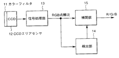
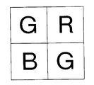
以下、本発明の実施の形態について図面を参照して詳細に説明する。図1は、本発明による画像処理装置の基本構成を示すブロック図である。ここで、本画像処理装置の処理対象となるカラー固体撮像素子は、色配列として例えば図2に示すR(赤)G(緑)B(青)の原色ベイヤ配列のカラーフィルタ11を受光面上に有する単板式固体撮像素子12である。
【0010】
なお、色配列は原色ベイヤ配列に限定されるものではなく、さらにカラーフィルタもRGBの原色の色配列に限られるものではなく、他の原色の色配列の場合でも、補色を使用した色配列(例えば、Ye/Cy/Mg/G)の場合でも同様に適応可能である。また、固体撮像素子12としては、全画素の信号電荷を独立に読み出すいわゆる全画素読み出し方式のCCD(Charge Coupled Device) 固体撮像素子(以下、CCDエリアセンサと称する)を用いるものとするが、全画素読み出し方式ではないCCD固体撮像素子にも適応可能である。
【0011】
CCDエリアセンサ12から出力されるRGB点順次データは、信号処理部13において黒レベルクランプやホワイトバランスなどの信号処理が行われた後、検出部14および補間部15に供給される。検出部14は、入力されるRGB点順次データから最適な補間方法を検出し、その補間情報を補間部15へ送る。補間部15は、検出部14から入力される補間情報を基にRGB点順次データに対して補間処理を行って出力する。
【0012】
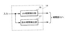
検出部14は、図3に示すように、補間画素に関して上下および左右の互いに90°の整数倍の角度をなす4方向、即ち垂直(V)方向の相反する2方向および水平(H)方向の相反する2方向の計4方向の相関の程度を検出するVH相関検出部16と、補間画素に関して右上、左上、左下、右下の斜め方向、即ち上記4方向に対してそれぞれ45°の角度をなす4方向の相関の程度を検出する斜め相関検出部17とを有する構成となっている。
【0013】
なお、本例では、上下左右4方向に加え、斜め4方向の計8方向の相関の程度を検出する構成を例に採っているが、上下左右の4方向だけの相関の程度を検出する構成であっても良い。ただし、以下の説明では、8方向の場合を例に採って説明するものとする。
【0014】
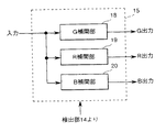
一方、補間部15は、図4に示すように、検出部14から与えられる補間情報に基づいて、Gの画素情報に対して補間処理を行うG補間部18と、Rの画素情報に対して補間処理を行うR補間部19と、Bの画素情報に対して補間処理を行うB補間部20とを有する構成となっている。
【0015】
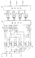
図5は、VH相関検出部16および斜め相関検出部17の具体的な構成の一例を示すブロック図である。
【0016】
VH相関検出部16は、補間画素の右側の画素の画素情報に基づいて相関の程度を示す相関値を算出する右側相関値算出回路21と、補間画素の左側の画素の画素情報に基づいて相関値を算出する左側相関値算出回路22と、補間画素の上側の画素の画素情報に基づいて相関値を算出する上側相関値算出回路23と、補間画素の下側の画素の画素情報に基づいて相関値を算出する下側相関値算出回路24と、これら相関値算出回路21〜24で算出した各相関値を補間ゲインに変換して出力する相関値→補間ゲイン変換回路25とから構成されている。
【0017】
上記構成のVH相関検出部16において、相関値→補間ゲイン変換回路25からは、水平垂直補間用ゲインRGain,LGain,TGain,BGainおよび水平垂直RB補間用ゲインRGainD,LGainD,TGainD,BGainDが補間係数として出力される。なお、水平垂直RB補間用ゲインRGainD,LGainD,TGainD,BGainDについては、後で詳述する。
【0018】
斜め相関検出部17は、補間画素の右上側の画素の画素情報に基づいて相関値を算出する右上側相関値算出回路26と、補間画素の左上側の画素の画素情報に基づいて相関値を算出する左上側相関値算出回路27と、補間画素の左下側の画素の画素情報に基づいて相関値を算出する左下側相関値算出回路28と、補間画素の右下側の画素の画素情報に基づいて相関値を算出する右下側相関値算出回路29と、これら相関値算出回路26〜29で算出した各相関値を補間ゲインに変換し、補間係数として斜め補間用ゲインD1Gain〜D4Gainを出力する相関値→補間ゲイン変換回路30とから構成されている。
【0019】
さらに、水平垂直4方向と斜め4方向は互いに直交していないため、VH‐斜め比較回路31において、水平垂直の相関値と斜めの相関値を比較することにより、斜め補間補正用ゲインVHGain,DGainを補間係数として算出するようにしている。この斜め補間補正用ゲインVHGain,DGainの算出法については、後で詳細に説明する。
【0020】
図6は、VH相関検出部16における例えば左側相関値算出回路22の具体的な構成の一例を示すブロック図である。なお、右側相関値算出回路21、上側相関値算出回路23および下側相関値算出回路24についても、全く同じ回路構成を採る。
【0021】
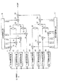
左側相関値算出回路22において、入力されたRGB点順次信号は、色分離回路32において、R画素/G画素/B画素の各色にそれぞれ対応するR信号/G信号/B信号に分離されて出力される。G信号は、変化量1,2算出回路33,34にそれぞれ供給される。R信号は、変化量算出回路35に供給される。B信号は、変化量算出回路36に供給される。
【0022】
ここで、G信号についてのみ、2つの異なる変化量1,2算出回路33,34に入力するのは、図2のRGB原色ベイヤ配列を見ても分かるように、GはR/Bに比べて水平方向および垂直方向のサンプリング数が倍であり、Gでは隣り合った垂直ラインでの変化量1と、1ラインおいた垂直ライン同士での変化量2を算出するためである。なお、ここでは、隣り合った垂直ライン間または1ラインおいた垂直ライン間での例を採ったが、2ライン以上おいた垂直ライン間であっても良い。
【0023】
変化量1,2算出回路33,34および変化量算出回路35,36は、図7の概念図に示すように、変化量を算出する方向に対して直交する向きにしたLPF(1,2,2,2,1)37,38,39を通した後に、算出用BPF40,41,42,43を通すことにより変化量を算出する構成となっている。ここで、算出用BPF40,41,42,43は、Gについては1/2相関(1,−1)と、1/4相関(1,0,−1)を使用し、R/Bについては1/4相関(1,1,−1,−1)を使用する。
【0024】
これら変化量算出回路33,34,35,36で算出された各変化量は、絶対値化回路45,46,47,48で絶対値化された後係数付加回路49,50,51,52に供給される。係数付加回路49,50,51,52は、絶対値化回路45,46,47,48で絶対値化された各変化量に対して別途設定された係数をそれぞれ掛け合わせて出力する。そして、係数付加回路49,50,51,52の各出力は、加算回路53で加え合わされた後、上下左右の相関値St,Sb,Sl,Srとして出力される。なお、RBの相関値への寄与がGに比べて低くなるように1/4して加算する。
【0025】
ここで、係数付加回路49,50,51,52において係数を掛ける理由は、R/G/Bの各色は輝度を形成する際にも、NTSCテレビジョン方式の場合には0.30R+0.59G+0.11Bとして計算するように、人間の視覚特性に合わせるためである。ただし、計算量やゲート規模を削減するためには、R:G:Bが3:6:1の比率、1:2:1の比率または2:4:1の比率になるように簡易的な係数を設定する方が良い。
【0026】
続いて、上記構成の左側相関値算出回路22における変化量算出回路33〜36による左方向の変化量の算出法につき、図8の原色ベイヤ配列図を用いて説明する。ここでは、左方向の変化量の算出法について述べるが、他の方向(右/上/下の各方向)についても、添え字が変わるだけで全く同じである。
【0027】
先ず、Gについては、隣り合った垂直ラインでの変化量が(1)式により、1ラインおいた垂直ライン同士での変化量が(2)式によりそれぞれ算出される。なお、(1)式/(2)式では、画素G22に対する相関を検出する際の式を示している。一方、R信号/B信号では、1ラインおきにしか同じ色の信号が存在しないため、1ラインおいた垂直ライン間の変化量が、(3)式/(4)式によりそれぞれ算出される。また、画素G33に対しては、水平/垂直を表わす添え字がそれぞれ1ずつ増加する他に、R信号とB信号で算出方法が入れ替わる。
【0028】
【数1】

図5に示すVH相関検出部16において、相関係数を決定する回路である相関値→相関ゲイン変換回路25は、相関係数を決定するに当り、相関値算出回路21〜24で算出された4方向の相関値Sr,Sl,St,Sbを基に、相関モードを決定する。相関モードを導入する理由は、単に相関値を順位付けした場合では、相関の順位に対して補間係数の決定が難しいためである。
【0030】
例えば、4つの相関値がほとんど同じである場合(100,101,102,103)と、全く異なる場合(0,10,100,500)では、補間係数の算出結果は異なるべきである。そこで、相関の順位決定とは別に相関係数の分布を示す相関モードを導入する。相関モードは、4つの相関値Sr,Sl,St,Sbがどういう分布になっているかを表わすもので、表1に示すように、0から7までの8つのモードからなる。
【0031】
【表1】
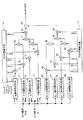
図9は、相関モードを決定するための相関モード決定回路の具体的な構成の一例を示すブロック図である。
【0033】
図9において、4つの相関値Sr,St,Sl,Sbをそれぞれ比較するための6個のコンパレータ54〜59が設けられている。右方向の相関値Srは、コンパレータ54,55,57の各一方の比較入力Aとなる。上方向の相関値Stは、コンパレータ54の他方の比較入力Bになるとともに、コンパレータ56,58の各一方の比較入力Aとなる。左方向の相関値Slは、コンパレータ55,56の各他方の比較入力Bになるとともに、コンパレータ59の一方の比較入力Aとなる。下方向の相関値Sbは、コンパレータ57,58,59の各他方の比較入力Bとなる。
【0034】
ここで、コンパレータ54〜59は、2つの比較入力A,Bを比較することにより、“>”(大),“<”(小),“=”(等価)の3段階の比較結果を出力する構成となっている。すなわち、A>B,A<Bの2つの比較結果に加え、比較する2つの相関値の差の絶対値が、あるリファレンス値THよりも小さい場合は“=”であるとする。なお、このリファレンス値THとしては、補間画素の近傍の画素の平均レベルまたは加重平均レベル、例えば補間画素の近傍での輝度Y0にある係数を掛けたものを使用する。図10は、輝度Y0の検出の概念図である。
【0035】
コンパレータ54〜59の後段には、右、上、左、下にそれぞれ対応した4個の1ビット全加算器60〜63が設けられている。全加算器60は、コンパレータ54の比較結果A>Bを一方の加算入力X、コンパレータ55の比較結果A>Bを他方の加算入力Y、コンパレータ57の比較結果A>Bを桁上げ入力Cとする。全加算器61は、コンパレータ54の比較結果A<Bを一方の加算入力X、コンパレータ56の比較結果A>Bを他方の加算入力Y、コンパレータ58の比較結果A>Bを桁上げ入力Cとする。
【0036】
全加算器62は、コンパレータ55の比較結果A<Bを一方の加算入力X、コンパレータ56の比較結果A<Bを他方の加算入力Y、コンパレータ59の比較結果A>Bを桁上げ入力Cとする。全加算器63は、コンパレータ57の比較結果A<Bを一方の加算入力X、コンパレータ58の比較結果A<Bを他方の加算入力Y、コンパレータ59の比較結果A<Bを桁上げ入力Cとする。そして、これら全加算器60〜63は、2つの加算入力X,Yおよび桁上げ入力Cに基づいて自分の順位を判定し、判定結果S0,S1を出力する。
【0037】
全加算器60〜63の各判定結果S0,S1は、論理回路64を経て4個の4入力加算器65〜68に供給される。これら加算器65〜68のうち、加算器65,66からは2つの加算出力S0,S1が、加算器67,68からは1つの加算出力S0がそれぞれ導出され、論理回路69に入力される。この論理回路69は、加算器65,66の各2つの加算出力S0,S1と、加算器67,68の各1つの加算出力S0に基づいて3ビットのモード信号m0,m1,m2を出力する。このモード信号m0,m1,m2に基づいて8つのモードが決定される。
【0038】
上記構成の相関モード決定回路において、4つの相関値Sr,Sl,St,Sbをそれぞれ比較して3段階の比較結果(“>”,“<”,“=”)を得、これら比較結果を基に小さい順に0から順位をつける。この場合に、2ないし4方向が同じ順位になる場合もある。この順位の分布を基に表1に当てはめ、相関モードを決定する。なお、Mode1,2,5,6の場合では、分布が表とは異なる場合がある。例えば、Mode1では順位0が3方向で、残りの1方向の順位は1,2,3のどれでもあり得る。
【0039】
続いて、相関順位からランク付けを行う。ここで、ランクと相関順位とは、便宜上、別なものである。ランクとは、同じ相関順位にある方向に対しても順番を付けたものである。同じ相関順位の場合の順番の付け方は、“右”から時計周りとする。例えば、上下左右が全て同じ相関順位であった場合は、右、上、左、下のランクはそれぞれ0,1,2,3となる。
【0040】
以上のようにして、相関値→相関ゲイン変換回路25において、相関係数を算出する際に相関モードとランクを決定し、この組み合わせによってそれぞれのランクの補間係数を算出することにより、各方向の補間係数、即ち水平垂直補間用ゲインRGain,LGain,TGain,BGainおよび水平垂直RG補間用ゲインRGainD,LGainD,TGainD,BGainDを決定できる。
【0041】
ここで、補間係数を算出するに当り、相関値→相関ゲイン変換回路25では、決定した相関モードにより補間係数の算出方法を変える構成を採っている。すなわち、水平垂直4方向の4つの相関値Sr,Sl,St,Sbにおいて、その値の小さいものから順にS0,S1,S2,S3とし、これらに基づいて各モードごとに例えばルックアップテーブル(LUT)から変数α(0≦α≦1/4)を求め、この変数αを用いて補間係数を算出するようにする。
【0042】
すなわち、図11に示すように、4つの相関値S0〜S3を演算回路70Aにおいて演算してS3−S0,S2−S0,S1−S0の3つの演算出力を得る。この3つの演算出力S3−S0,S2−S0,S1−S0を、選択回路70Bにおいて、3ビットのモード信号m0〜m2で決まる各モードに対応して選択してルックアップテーブル70Cに与えるようにする。
【0043】
ルックアップテーブル70Cにおいては、モード0ではα=0とし、モード1ではS3−S0の値に対応する変数αを、モード2またはモード3ではS2−S0の値に対応する変数αを、モード4以降ではS1−S0の値に対応する変数αをそれぞれ設定する。そして、この変数αを用いて表2のように補間係数を算出するようにする。なお、ルックアップテーブル70Cのテーブル値を外部から変更可能とすることで、変数αの値を任意に設定することができる。
【0044】
【表2】
以上、水平垂直4方向の相関検出について述べたが、斜め4方向の相関検出に関しては、色分離後のRGBの各信号に対し、それぞれ斜め方向の変調成分の絶対値を算出し、R:G:B=1:4:1の割合で加算し、相対値とする。なお、右上、左上、左下、右下をそれぞれ、D1方向、D2方向、D3方向、D4方向とする。そして、図5の相関値→補間ゲイン変換回路30において、水平垂直4方向の場合と同様にして、斜め4方向の補間用ゲインD1Gain,D2Gain,D3Gain,D4Gainを補間係数として算出する。
【0046】
次に、図4の補間部15におけるG,R,Bの各補間部18,19,20の具体的な構成の一例を図12および図13に示す。なお、図12はG補間部18の構成を、図13はR,B補間部19,20の構成をそれぞれ示している。
【0047】
先ず、図12において、色分離後のGのデータは水平垂直4方向、即ち右側、左側、上側、下側の各相関用処理回路71,72,73,74にそれぞれ供給され、これら相関用処理回路71,72,73,74において4方向の補間データGr,Gl,Gt,Gbが生成される。これら補間データGr,Gl,Gt,Gbは、補間する方向にLPFを通すことで生成される。実際には、高輝度用と低輝度用の2つのLPFを設け、それぞれの出力に所定のゲインを掛けた後に加算することで、補間データGr,Gl,Gt,Gbの生成が行われる。
【0048】
補間データGr,Gl,Gt,Gbは各々、乗算器75,76,77,78において、図5に示すVH相関検出部16で決定された補間係数、即ち水平垂直補間用ゲインRGain,LGain,TGain,BGainがそれぞれ掛けられる。そして、加算器79〜81によって加算されることにより、Gの補間処理が行われる。補間処理後のGの画像データは、(5)式で表される。
G=Gr×RGain+Gl×LGain
+Gt×TGain+Gb×BGain ……(5)
【0049】
斜め4方向についても同様に、右上側、左上側、左下側、右下側の各相関用処理回路82,83,84,85において、D1/D2/D3/D4の各方向の補間データが生成され、乗算器86,87,88,89において、図5に示す斜め相関検出部17で決定された斜め補間用ゲインD1Gain,D2Gain,D3Gain,D4Gainがそれぞれ掛けられた後、加算器90〜92で足し合わされることによって補間処理が行われる。
【0050】
また、水平垂直4方向相関検出/補間によるGの画像データと、斜め4方向相関検出/補間によるGの画像データを、状況に合わせて(6)式に示すように混合比を変化させて加算する。混合比の調整は、図5に示すVH‐斜め比較回路31で算出される斜め補間補正用ゲインVHGain,DGainによって行われる。
G=Gvh×VHGain+Gd×DGain ……(6)
【0051】
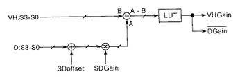
ここで、水平垂直方向と斜め方向は直交していないため、水平垂直と斜めのそれぞれの相関値の最大値S3と最小値S0の差(S3−S0)を比較し、この値の大きい方の補間係数が小さい方の補間係数よりも大きくなるように加算する。これは、検出方向に対して、平行または直交しているエッジの場合に、相関値の最大値と最小値の差が大きくなるためである。ただし、水平垂直と斜めの比較をする際に、水平垂直の算出値にオフセットを与え、標準で水平垂直補間を行い、斜め補間に適した場合にのみ斜め用の補間係数を大きくする。
【0052】
水平垂直と斜めのそれぞれの相関値の最大値S3と最小値S0の差(S3−S0)を比較する際には、図14の概念図に示すように、斜めの差(S3−S0)に対して所定の定数SDoffsetを加算(又は、減算)した値に係数SDGainを掛けた値Aを、水平垂直の差B(S3−S0)と比較し、その差(A−B)に基づいて斜め補間補正用ゲインVHGain,DGainを設定するようにする。
【0053】
すなわち、図12において、加算器81の出力データに対して乗算器93で斜め補間補正用ゲインVHGainを掛けるとともに、加算器92の出力データに対して乗算器94で補間補正用ゲインDGainを掛け、これら乗算器93,94の各出力データを加算器95で加算することにより、水平垂直4方向相関検出/補間によるGの画像データと、斜め4方向相関検出/補間によるGの画像データを所定の割合で混合(加算)するようにする。
【0054】
以上、G補間部18の構成および動作について説明したが、図13に示すR,B補間部19,20の構成についても、図12に示すG補間部18の構成と基本的には同じである。したがって、図13中、図12と同等部分には同一符号を付して示してある。ただし、右側、左側、上側、下側の各相関用処理回路71′,72′,73′,74′における補間データの生成法については、Gの場合に比べて複雑である。その理由として2つあり、RB補間用相関検出を行うことと、G/2成分をRBに加えるためである。
【0055】
そのため、RG補間用相関検出は、水平(右、左)の補間データ用と垂直方向(上、下)の補間データ用では別々に行う。具体的には、R画素およびB画素の信号からR信号/B信号を補間する際に、先述した水平垂直RB補間用ゲインRGainD,LGainD,TGainD,BGainDを、R/B専用の補間係数として算出して用いる。以下、R信号の補間処理を例に採って説明するが、B信号の補間処理についても同様である。
【0056】
なお、RGBの原色ベイヤ配列のカラーフィルタ11において、その色配列を示す図2から明らかなように、Gは水平方向または垂直方向の空間サンプリング数がCCDエリアセンサ12の全画素による空間サンプリング数と同じであるのに対し,R/Bは水平方向または垂直方向の空間サンプリング数がCCDエリアセンサ12の全画素による空間サンプリング数に比べて少ない。
【0057】
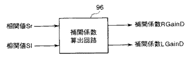
図8に示す原色ベイヤ配列において、補間すべき画素がR21の画素の場合では特別な処理は必要なく、R21の信号をそのままR信号として使用する。補間すべき画素がG22の場合は、左側補間はR21の画素を、右側補間はR23の画素を使用するが、上側補間と下側補間の場合では、図15に示す補間係数算出回路96を用いるようにする。この補間係数算出回路96は、図5のVH相関検出部16における相関値→相関ゲイン変換回路25の一部を構成している。
【0058】
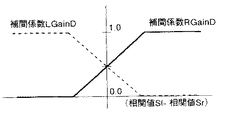
すなわち、VH相関検出部16において、右側相関値算出回路21で算出した右側相関値Srと左側相関値算出回路22で算出した左側相関値Slを補間係数算出回路96に入力し、この補間係数算出回路96によって右側補間係数RGainDと左側補間係数LGainDを算出する。この補間係数算出回路96の特性の一例を図16に示す。なお、図16の特性では、補間係数が0.0〜1.0の範囲のように示してあるが、補間係数の値そのものはいくつでも良く、実際に補間係数とR信号とを掛け合わせたときに結果的に0.0〜1.0の範囲に入れば問題ない。
【0059】
このようにして算出された右側補間係数RGainDと左側補間係数LGainDが、図13の右側相関用処理回路71′および左側相関用処理回路72′に入力されると、これら相関用処理回路71′,72′において、所定の演算処理が行われ、上側補間データTDataと下側補間値BDataが算出される。相関用処理回路71′,72′における演算式としては、
TData=R01×LGainD+R03×RGainD
BData=R41×LGainD+R43×RGainD
【0060】
または、
TData={(R01+R21)×LGainD
+(R03+R23)×RGainD}/2
BData={(R21+R41)×LGainD
+(R23+R43)×RGainD}/2
などが考えられる。
【0061】
また、補間すべき画素G33の場合には、上記と同様な処理方法で上側相関値St/下側相関値Sbから上側補間係数TGainD/下側補間係数BGainDを算出し、例えば次のような演算式にて右側補間データRData/左側補間データLDataを算出する。
LData=R21×TGainD+R41×BGainD
RData=R25×TGainD+R45×BGainD
【0062】
さらに、補間すべき画素がB32の場合では、上側相関値St/下側相関値Sbから上側補間係数TGainD/下側補間係数BGainDを、右側相関値Sr/左側相関値Slから右側補間係数RGainD/左側補間係数LGainDをそれぞれ算出し、次のような演算式にて上側補間データTData/下側補間データBData/左側補間データLData/右側補間データRDataをそれぞれ算出する。
TData=R21×LGainD+R23×RGainD
BData=R41×LGainD+R43×RGainD
LData=R21×TGainD+R41×BGainD
RData=R23×TGainD+R43×BGainD
【0063】
上述したように、RG補間用相関検出は、水平方向(右、左)の補間データ用と垂直方向(上、下)の補間データ用とで別々に行う。水平方向の補間データ用補間係数LGainD,RGainDには、右側相関値Srと左側相関値Slを比較(Sl−Sr)して算出する。垂直方向の補間データ用補間係数TGainD,BGainDには、上側相関値Stと下側相関値Sbを比較(Sb−St)して算出する。
【0064】
そして、これら補間係数TGainD/BGainD/LGainD/RGainDに基づいて上側補間データTData/下側補間データBData/左側補間データLData/右側補間データRDataをそれぞれ算出した後、図5のVH相関検出部16で算出した4方向相関検出による水平垂直補間用係数TGain/BGain/LGain/RGainを掛け合わせて加算し、R信号を生成する。
【0065】
ここで、Rの上側補間データTDataを生成する場合を例にとって考える。Rは元画像には水平垂直ともに1画素おきにしか情報がないため、補間すべき画素がR画素の場合はその画素のデータを使用し、Gb画素の場合では上側がR画素であるため、上側のR画素のデータを上側補間データとする。
【0066】
しかし、B画素またはGr画素の場合では、その垂直ライン上にRの情報がないため、左右の垂直ラインのR画素とGの1/2変調成分を基に上側補間データTDataを生成する。具体的には、右側垂直ライン上のR画素と水平右側のGの1/2変調成分を加算したものにRGainDを係数として掛け合わせ、左側垂直ライン上のR画素と水平左側のGの1/2変調成分を加算したものにLGainDを係数として掛け合わせて足すことにより、上側補間データTDataを生成する。
【0067】
ところで、図8に示す原色ベイヤ配列において、G22の画素に相当するR信号の補間を行う場合、水平方向の補間に関しては両側がRであり、Rが疎であるため問題ないが、垂直方向の補間を行うとしても同一の垂直ラインではG02,B12,G22,B32,G42のようにG信号またはB信号のみしか存在しない。このため、隣りの垂直ラインのR信号を用いる必要がある。
【0068】
しかし、水平方向で信号レベルが急激に変化するような垂直のエッジを撮像すると、エッジがG22の垂直ラインと隣りの例えばR23の垂直ラインの間にくることがある。この場合には、G22の位置のR信号のレベルはR01/R21/R41などとはほぼ等しくなるべきだが、R03/R23/R43などのR信号のレベルを使用するため、本来の信号レベルとは異なり、エッジに色が着くことが懸念される。
【0069】
ところが、原色ベイヤ配列の信号処理において、上述したように、R画素およびB画素の信号からR信号/B信号を補間する際に、右側相関値Srと左側相関値Slに基づいて水平方向の補間データ用補間係数LGainD,RGainDを、上側相関値Stと下側相関値Sbに基づいて垂直方向の補間データ用補間係数TGainD,BGainDを算出して用いるようにしたことで、エッジ部の色付き(色偽信号)を抑圧しつつ、4方向相関検出補間処理による解像度/解像感の向上が可能となる。
【0070】
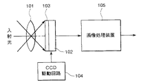
図17は、本発明に係るカメラの一例を示す概略構成図である。図17において、被写体からの入射光は、レンズ101等を含む光学系によってCCDエリアセンサ102の受光面(撮像面)上に結像される。CCDエリアセンサ102の受光面上には、色配列が例えば原色ベイヤ配列のカラーフィルタ103が設けられている。CCDエリアセンサ102は、CCD駆動回路104によって露光、信号電荷の読み出しおよび転送などの駆動制御が行われる。
【0071】
CCDエリアセンサ102の出力信号は画像処理装置105に供給され、種々の信号処理が行われる。この画像処理装置105として、水平垂直および斜めの8方向の相関を検出し、その検出結果に基づいて適応型補間処理を行う上記実施形態に係る画像処理装置が用いられる。
【0072】
このように、例えば原色ベイヤ配列のカラーフィルタ103を持つCCDエリアセンサ102を撮像デバイスとして用いたカメラにおいて、水平垂直および斜めの8方向の相関を検出し、その検出結果に基づいて適応型補間処理を行うようにしたことで、カラーフィルタ103上において各色が飛び飛びに存在しても、解像感を損なうことがないとともに、折れ曲がった線や、直角に曲がった角の部分などにおいても良好に補間処理が行われるので、より良好な撮像画像を得ることができる。
【0073】
【発明の効果】
以上説明したように、本発明によれば、カラーフィルタを受光面上に有する固体撮像素子から出力される画像信号に対して、補間すべき画素とその周辺画素との相関を検出して色補正処理を行う際に、前記補間すべき画素に関して補間する方向にローパスフィルタを通すことによって得られる補間データに補間係数を乗算し、その乗算結果を加算することによって補間処理を行う際に、補間画素に関して左右および上下の4方向に対応する画素情報に基づいてその4方向に対する相関値を算出し、この算出した4方向に対する相関値の各々の大小関係に応じて相関モードを決定し、その相関モードにより算出方法を変えて補間係数を決定し、この決定した補間係数に基づいて上記4方向に対応する画素情報を基に補間処理を行うようにしたことにより、相関値の算出方向に対して直交していない方向のエッジに対しても、良好に相関の度合いを判定できるため、補間処理後の斜めエッジがぼやけることなく良好に再現できるとともに、折れ曲がった線や、直角に曲がった角の部分などにおいても良好に補間することが可能となる。
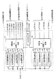
【図面の簡単な説明】
【図1】本発明による画像処理装置の基本構成を示すブロック図である。
【図2】カラーフィルタの原色ベイヤ配列図である。
【図3】検出部の構成の一例を示すブロック図である。
【図4】補間部の構成の一例を示すブロック図である。
【図5】VH相関検出部および斜め相関検出部の具体的な構成の一例を示すブロック図である。
【図6】相関値算出回路の具体的な構成の一例を示すブロック図である。
【図7】変化量の算出の概念図である。
【図8】変化量の算出法を説明するための原色ベイヤ配列図である。
【図9】相関モード決定回路の具体的な構成の一例を示すブロック図である。
【図10】輝度Y0の検出の概念図である。
【図11】変数αを算出する回路の具体的な構成の一例を示すブロック図である。
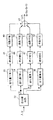
【図12】G補間部の具体的な構成の一例を示すブロック図である。
【図13】R,B補間部の具体的な構成の一例を示すブロック図である。
【図14】斜め補間補正用ゲインの算出の概念図である。
【図15】水平垂直RB補間係数を算出するための構成図である。
【図16】補間係数算出回路の特性の一例を示す特性図である。
【図17】本発明に係るカメラの一例を示す概略構成図である。
【符号の説明】
11…カラーフィルタ、12…CCDエリアセンサ、14…検出部、15…補間部、16…VH相関検出部、17…斜め相関検出部、18…G補間部、19…R補間部、20…B補間部、21〜24,26〜29…相関値算出回路、25,30…相関値→相関ゲイン変換回路、31…VH‐斜め比較回路、33〜36…変化量算出回路、37〜39…LPF(ローパスフィルタ)、45〜48…絶対値化回路、49〜52…係数付加回路、54〜59…コンパレータ、96…補間係数算出回路[0001]
BACKGROUND OF THE INVENTION
The present invention relates to an image processing apparatus, an image processing method, and a camera, and more particularly to an image processing apparatus and an image processing method for processing an output signal of a solid-state imaging device having a color filter of a predetermined color arrangement on a light receiving surface, and It relates to the camera used.
[0002]
[Prior art]
In an image processing apparatus that processes an output signal of a solid-state imaging device having a color filter of, for example, a primary color Bayer array on the light receiving surface, each color is scattered on the color filter so that the resolution is not impaired. Interpolation processing is performed to achieve this. In this type of image processing apparatus, conventionally, correlation values in only two directions, such as two opposite directions in the horizontal direction (left and right direction) or two opposite directions in the vertical direction (up and down direction), are calculated and used as the basis. Interpolation processing was performed. In other words, whether horizontal stripes or vertical stripes are determined from the pixel information of, for example, a 5 × 5 pixel area around the pixel to be interpolated, and in the case of horizontal stripes, interpolation is performed using the signals of pixels on both sides in the horizontal direction of the pixel to be interpolated. In the case of vertical stripes, interpolation is performed using the signals of pixels on both sides in the vertical direction.
[0003]
[Problems to be solved by the invention]
However, in the conventional image processing apparatus that performs interpolation by detecting the correlation in only two directions, it is effective for the edge portion in the horizontal direction or the vertical direction, but one pixel is also used for the oblique edge portion or the edge in the horizontal / vertical direction. In the case of a line segment of about the width, it is not possible to detect an appropriate edge at the intersection of the horizontal edge and the vertical edge, or in the bent part of the line segment, and in the case of an oblique line, is the horizontal correlation strong? Whether or not the vertical correlation is strong cannot be determined, and the process of averaging the horizontal edge portion process and the vertical edge portion process (average value interpolation) tends to be performed.
[0004]
For this reason, in the conventional image processing apparatus, in the portion shown in the above example, there is a problem that the image is blurred with no resolution, or the line is interrupted in a portion that should not be interrupted. become.
[0005]
The present invention has been made in view of the above problems, and an object of the present invention is to provide an image processing apparatus capable of performing satisfactory interpolation processing even in a bent line or a corner portion bent at a right angle. And providing an image processing method.
[0006]
[Means for Solving the Problems]
An image processing apparatus according to the present invention includes a solid-state imaging device having a color filter having a predetermined color arrangement on a light receiving surface.Is obtained by passing a low-pass filter in the direction of interpolation with respect to the pixel to be interpolated when color correlation processing is performed by detecting the correlation between the pixel to be interpolated and its surrounding pixels. Interpolation processing is performed by multiplying the interpolation data by the interpolation coefficient and adding the multiplication results.An image processing apparatus, which forms an angle that is an integral multiple of 90 ° with respect to a pixel to be interpolated (hereinafter referred to as an interpolated pixel).Pixel information corresponding to 4 directionsA correlation value calculation circuit for calculating a correlation value for the four directions based on the correlation value, a coefficient determination circuit for determining an interpolation coefficient based on the correlation values for the four directions calculated by the correlation value calculation circuit, and the coefficient determination circuit Using the interpolation coefficient determined in
[0007]
The image processing method according to the present invention also includes a solid-state imaging device having a color filter having a predetermined color arrangement on a light receiving surface.Is obtained by passing a low-pass filter in the direction of interpolation with respect to the pixel to be interpolated when color correlation processing is performed by detecting the correlation between the pixel to be interpolated and its surrounding pixels. Interpolation processing is performed by multiplying the interpolation data by the interpolation coefficient and adding the multiplication results.An image processing method that forms an angle that is an integral multiple of 90 ° on the left, right, and top and bottom with respect to an interpolated pixelPixel information corresponding to 4 directionsCalculate correlation values for the four directions based onCalculation step to,thisIn the calculation stepInterpolation coefficient is determined based on the calculated correlation values for the four directionsWith a decision step to,thisIn the decision stepBased on the determined interpolation coefficient in the above four directionsCorresponding pixel informationPerform interpolation processing based onAnd a processing step. In the determining step, a correlation mode is determined according to the magnitude relationship of the correlation values with respect to the four directions, and the calculation method of the interpolation coefficient is changed according to the correlation mode.
[0008]
In the image processing apparatus having the above configuration and its processing method, first, a characteristic value for a total of four directions of the interpolated pixel, that is, left and right (horizontal direction) and up and down (vertical direction), that is, a correlation value indicating a degree (degree) of correlation is calculated. . Next, based on the correlation values for the four directions, an interpolation coefficient used at the time of interpolation is determined.In determining the interpolation coefficient, the correlation mode is determined according to the magnitude relationship of the correlation values with respect to the four directions, and the calculation method of the interpolation coefficient is changed depending on the correlation mode.And used to calculate the correlation valuePixel information corresponding to 4 directionsInterpolation processing is performed by multiplying the interpolation coefficients and adding them.
[0009]
DETAILED DESCRIPTION OF THE INVENTION
Hereinafter, embodiments of the present invention will be described in detail with reference to the drawings. FIG. 1 is a block diagram showing a basic configuration of an image processing apparatus according to the present invention. Here, the color solid-state imaging device to be processed by the image processing apparatus uses, for example, the color filter 11 of the primary color Bayer array of R (red) G (green) B (blue) shown in FIG. This is a single plate type solid-state imaging device 12.
[0010]
Note that the color arrangement is not limited to the primary color Bayer arrangement, and the color filter is not limited to the RGB primary color arrangement, and even in the case of other primary color arrangements, a color arrangement using complementary colors ( For example, the case of Ye / Cy / Mg / G) can be similarly applied. Further, as the solid-state imaging device 12, a so-called all-pixel readout type CCD (Charge Coupled Device) solid-state imaging device (hereinafter referred to as a CCD area sensor) that reads out signal charges of all the pixels independently is used. The present invention can also be applied to a CCD solid-state imaging device that is not a pixel readout method.
[0011]
The RGB point sequential data output from the CCD area sensor 12 is subjected to signal processing such as black level clamping and white balance in the
[0012]
As shown in FIG. 3, the
[0013]
In this example, a configuration that detects the degree of correlation in a total of eight directions in four oblique directions in addition to the four directions in the upper, lower, left, and right directions is used as an example. It may be. However, in the following description, the case of 8 directions will be described as an example.
[0014]
On the other hand, as illustrated in FIG. 4, the
[0015]
FIG. 5 is a block diagram illustrating an example of a specific configuration of the VH
[0016]
The VH
[0017]
In the VH
[0018]
The oblique
[0019]
Further, since the four horizontal and vertical directions and the four oblique directions are not orthogonal to each other, the VH-
[0020]
FIG. 6 is a block diagram illustrating an example of a specific configuration of, for example, the left correlation
[0021]
In the left correlation
[0022]
Here, only the G signal is input to the two
[0023]
As shown in the conceptual diagram of FIG. 7, the
[0024]
The change amounts calculated by the change
[0025]
Here, the reason for multiplying the coefficients in the
[0026]
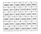
Next, a method of calculating the amount of change in the left direction by the amount of
[0027]
First, for G, the amount of change between adjacent vertical lines is calculated from equation (1), and the amount of change between one vertical line is calculated from equation (2). In addition, in Formula (1) / Formula (2), the formula at the time of detecting the correlation with respect to the pixel G22 is shown. On the other hand, in the R signal / B signal, the same color signal exists only every other line, and therefore, the amount of change between the vertical lines of one line is calculated by the equations (3) / (4). Further, for the pixel G33, the subscript indicating horizontal / vertical is increased by 1, and the calculation method is switched between the R signal and the B signal.
[0028]
[Expression 1]
In the VH
[0030]
For example, when the four correlation values are almost the same (100, 101, 102, 103) and when they are completely different (0, 10, 100, 500), the interpolation coefficient calculation results should be different. Therefore, a correlation mode indicating the distribution of correlation coefficients is introduced separately from the correlation order determination. The correlation mode represents the distribution of the four correlation values Sr, S1, St, and Sb. As shown in Table 1, the correlation mode includes eight modes from 0 to 7.
[0031]
[Table 1]
FIG. 9 is a block diagram showing an example of a specific configuration of a correlation mode determination circuit for determining a correlation mode.
[0033]
In FIG. 9, six
[0034]
Here, the
[0035]
At the subsequent stage of the
[0036]
The
[0037]
The determination results S0 and S1 of the
[0038]
In the correlation mode determination circuit configured as described above, the four correlation values Sr, S1, St, and Sb are respectively compared to obtain three levels of comparison results (“>”, “<”, “=”). Based on the order starting from 0 in ascending order. In this case, 2 to 4 directions may have the same order. Based on this distribution of rank, the correlation mode is determined according to Table 1. In the case of
[0039]
Subsequently, ranking is performed from the correlation order. Here, the rank and the correlation order are different for convenience. The rank is an order with respect to directions in the same correlation order. In the case of the same correlation order, the ordering method is clockwise from “right”. For example, if the top, bottom, left, and right have the same correlation rank, the ranks of right, top, left, and bottom are 0, 1, 2, and 3, respectively.
[0040]
As described above, in the correlation value → correlation
[0041]
Here, in calculating the interpolation coefficient, the correlation value → correlation
[0042]
That is, as shown in FIG. 11, four correlation values S0 to S3 are calculated in the
[0043]
In the look-up table 70C, α = 0 in
[0044]
[Table 2]
Although the correlation detection in the four horizontal and vertical directions has been described above, for the correlation detection in the four diagonal directions, the absolute value of the modulation component in the diagonal direction is calculated for each RGB signal after color separation, and R: G : B = 1: 4: 1 is added to obtain a relative value. Note that the upper right, upper left, lower left, and lower right are defined as the D1, D2, D3, and D4 directions, respectively. Then, in the correlation value → interpolation
[0046]
Next, an example of a specific configuration of each of the G, R, and
[0047]
First, in FIG. 12, the color-separated G data is supplied to the
[0048]
The interpolation data Gr, Gl, Gt, and Gb are respectively multiplied by the interpolation coefficients determined by the VH
G = Gr x RGain + Gl x LGain
+ Gt × TGain + Gb × BGain (5)
[0049]
Similarly, in the four oblique directions, interpolation data in each direction of D1 / D2 / D3 / D4 is generated in the
[0050]
Further, G image data obtained by horizontal / vertical four-way correlation detection / interpolation and G image data obtained by oblique four-way correlation detection / interpolation are added by changing the mixing ratio according to the situation as shown in the equation (6). To do. The adjustment of the mixing ratio is performed by diagonal interpolation correction gains VHGain and DGain calculated by the VH-
G = Gvh × VHGain + Gd × DGain (6)
[0051]
Here, since the horizontal / vertical direction and the diagonal direction are not orthogonal, the difference between the maximum value S3 and the minimum value S0 (S3−S0) of the horizontal / vertical and diagonal correlation values is compared. Addition is performed so that the interpolation coefficient is larger than the smaller interpolation coefficient. This is because the difference between the maximum value and the minimum value of the correlation value becomes large in the case of an edge that is parallel or orthogonal to the detection direction. However, when the horizontal / vertical and diagonal are compared, an offset is given to the horizontal / vertical calculation value, horizontal / vertical interpolation is performed as a standard, and the diagonal interpolation coefficient is increased only when it is suitable for diagonal interpolation.
[0052]
When comparing the difference (S3−S0) between the maximum value S3 and the minimum value S0 of the horizontal and vertical correlation values, as shown in the conceptual diagram of FIG. 14, the diagonal difference (S3−S0) is calculated. A value A obtained by adding (or subtracting) a predetermined constant SDoffset to the coefficient SDGain is compared with a horizontal / vertical difference B (S3−S0), and the value A is obliquely determined based on the difference (A−B). The interpolation correction gains VHGain and DGain are set.
[0053]
That is, in FIG. 12, the
[0054]
Although the configuration and operation of the
[0055]
Therefore, the correlation detection for RG interpolation is performed separately for horizontal (right, left) interpolation data and vertical (up, down) interpolation data. Specifically, when the R signal / B signal is interpolated from the R pixel and B pixel signals, the above-described horizontal / vertical RB interpolation gains RGainD, LGainD, TGainD, and BGainD are calculated as interpolation coefficients dedicated to R / B. And use. The R signal interpolation processing will be described below as an example, but the same applies to the B signal interpolation processing.
[0056]
In the color filter 11 of the RGB primary color Bayer array, as is apparent from FIG. 2 showing the color array, G is the spatial sampling number in the horizontal direction or the vertical direction and the spatial sampling number by all pixels of the CCD area sensor 12. On the other hand, in the R / B, the spatial sampling number in the horizontal direction or the vertical direction is smaller than the spatial sampling number by all the pixels of the CCD area sensor 12.
[0057]
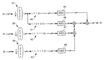
In the primary color Bayer array shown in FIG. 8, when the pixel to be interpolated is the R21 pixel, no special processing is required, and the R21 signal is used as it is as the R signal. When the pixel to be interpolated is G22, the left interpolation uses the R21 pixel, and the right interpolation uses the R23 pixel. However, in the case of the upper interpolation and the lower interpolation, the interpolation
[0058]
That is, the VH
[0059]
When the right interpolation coefficient RGainD and left interpolation coefficient LGainD calculated in this way are input to the right correlation processing circuit 71 'and the left correlation processing circuit 72' of FIG. 13, these correlation processing circuits 71 ', At 72 ′, a predetermined calculation process is performed, and upper interpolation data TData and lower interpolation value BData are calculated. As an arithmetic expression in the
TData = R01 × LGainD + R03 × RGainD
BData = R41 × LGainD + R43 × RGainD
[0060]
Or
TData = {(R01 + R21) × LGainD
+ (R03 + R23) × RGainD} / 2
BData = {(R21 + R41) × LGainD
+ (R23 + R43) × RGainD} / 2
And so on.
[0061]
In the case of the pixel G33 to be interpolated, the upper interpolation coefficient TGainD / lower interpolation coefficient BGainD is calculated from the upper correlation value St / lower correlation value Sb by the same processing method as described above. The right interpolation data RData / left interpolation data LData is calculated by the equation.
LData = R21 × TGainD + R41 × BGainD
RData = R25 × TGainD + R45 × BGainD
[0062]
Further, when the pixel to be interpolated is B32, the upper side correlation value St / lower side correlation value Sb is converted into the upper side interpolation coefficient TGainD / lower side interpolation coefficient BGainD, and the right side correlation value Sr / left side correlation value S1 is converted into the right side interpolation coefficient RGainD /. The left interpolation coefficient LGainD is calculated, and the upper interpolation data TData / lower interpolation data BData / left interpolation data LData / right interpolation data RData are calculated using the following arithmetic expressions.
TData = R21 × LGainD + R23 × RGainD
BData = R41 × LGainD + R43 × RGainD
LData = R21 × TGainD + R41 × BGainD
RData = R23 × TGainD + R43 × BGainD
[0063]
As described above, the correlation detection for RG interpolation is performed separately for the interpolation data in the horizontal direction (right and left) and the interpolation data in the vertical direction (up and down). For the interpolation coefficients LGainD and RGainD for the interpolation data in the horizontal direction, the right correlation value Sr and the left correlation value S1 are compared (S1−Sr). The vertical correlation data interpolation coefficients TGainD and BGainD are calculated by comparing the upper correlation value St and the lower correlation value Sb (Sb-St).
[0064]
Then, after calculating the upper interpolation data TData / lower interpolation data BData / left interpolation data LData / right interpolation data RData based on these interpolation coefficients TGainD / BGainD / LGainD / RGainD, the
[0065]
Here, a case where the upper interpolation data TData for R is generated will be considered as an example. Since R has information only every other pixel in both the horizontal and vertical directions in the original image, when the pixel to be interpolated is an R pixel, the data of that pixel is used, and in the case of a Gb pixel, the upper side is an R pixel. The upper R pixel data is used as upper interpolation data.
[0066]
However, in the case of the B pixel or the Gr pixel, there is no R information on the vertical line, so the upper interpolation data TData is generated based on the R pixel of the left and right vertical lines and the 1/2 modulation component of G. Specifically, the R pixel on the right vertical line and the horizontal half G modulation component are multiplied by RGainD as a coefficient, and the R pixel on the left vertical line and the horizontal
[0067]
By the way, in the primary color Bayer array shown in FIG. 8, when the R signal corresponding to the pixel of G22 is interpolated, there is no problem because both sides are R and R is sparse with respect to the horizontal direction interpolation. Even if interpolation is performed, only the G signal or the B signal exists in the same vertical line as in G02, B12, G22, B32, and G42. For this reason, it is necessary to use the R signal of the adjacent vertical line.
[0068]
However, when a vertical edge whose signal level changes rapidly in the horizontal direction is imaged, the edge may be between the vertical line of G22 and the adjacent vertical line of R23, for example. In this case, the level of the R signal at the position of G22 should be almost equal to that of R01 / R21 / R41 and the like, but since the level of the R signal such as R03 / R23 / R43 is used, what is the original signal level? Unlikely, there is a concern that the edge will be colored.
[0069]
However, in the primary color Bayer array signal processing, as described above, when the R signal / B signal is interpolated from the R pixel and B pixel signals, horizontal interpolation is performed based on the right correlation value Sr and the left correlation value S1. The interpolation coefficients LGainD and RGainD for data are used by calculating and using the interpolation coefficients TGainD and BGainD for the interpolation data in the vertical direction based on the upper correlation value St and the lower correlation value Sb. The resolution / resolution feeling can be improved by the four-way correlation detection interpolation process while suppressing the (false signal).
[0070]
FIG. 17 is a schematic configuration diagram illustrating an example of a camera according to the present invention. In FIG. 17, incident light from a subject is imaged on a light receiving surface (imaging surface) of a
[0071]
The output signal of the
[0072]
As described above, for example, in a camera using the
[0073]
【The invention's effect】
As described above, according to the present invention, the solid-state imaging device having the color filter on the light receiving surface.Is obtained by passing a low-pass filter in the direction of interpolation with respect to the pixel to be interpolated when color correlation processing is performed by detecting the correlation between the pixel to be interpolated and its surrounding pixels. Interpolation processing is performed by multiplying the interpolation data by the interpolation coefficient and adding the multiplication results.When interpolating pixels,Pixel information corresponding to 4 directionsThe correlation value for the four directions is calculated based on the above, and the calculated correlation value for the four directionsThe correlation mode is determined according to the magnitude relationship of each and the calculation method is changed depending on the correlation mode.An interpolation coefficient is determined, and the above is based on the determined interpolation coefficient.Pixel information corresponding to 4 directionsSince the interpolation process is performed based on this, the degree of correlation can be determined well even for edges that are not orthogonal to the correlation value calculation direction. In addition to being able to reproduce well without blurring, it is possible to satisfactorily interpolate even in a bent line or a corner portion bent at a right angle.
[Brief description of the drawings]
FIG. 1 is a block diagram showing a basic configuration of an image processing apparatus according to the present invention.
FIG. 2 is a primary color Bayer arrangement diagram of a color filter.
FIG. 3 is a block diagram illustrating an example of a configuration of a detection unit.
FIG. 4 is a block diagram illustrating an example of a configuration of an interpolation unit.
FIG. 5 is a block diagram illustrating an example of a specific configuration of a VH correlation detection unit and a diagonal correlation detection unit.
FIG. 6 is a block diagram illustrating an example of a specific configuration of a correlation value calculation circuit.
FIG. 7 is a conceptual diagram of calculation of a change amount.
FIG. 8 is a primary color Bayer array diagram for explaining a method of calculating a change amount;
FIG. 9 is a block diagram illustrating an example of a specific configuration of a correlation mode determination circuit.
FIG. 10 is a conceptual diagram of detection of luminance Y0.
FIG. 11 is a block diagram illustrating an example of a specific configuration of a circuit that calculates a variable α.
FIG. 12 is a block diagram illustrating an example of a specific configuration of a G interpolation unit.
FIG. 13 is a block diagram illustrating an example of a specific configuration of an R and B interpolation unit.
FIG. 14 is a conceptual diagram of calculation of a diagonal interpolation correction gain.
FIG. 15 is a configuration diagram for calculating horizontal / vertical RB interpolation coefficients;
FIG. 16 is a characteristic diagram illustrating an example of characteristics of an interpolation coefficient calculation circuit.
FIG. 17 is a schematic configuration diagram showing an example of a camera according to the present invention.
[Explanation of symbols]
DESCRIPTION OF SYMBOLS 11 ... Color filter, 12 ... CCD area sensor, 14 ... Detection part, 15 ... Interpolation part, 16 ... VH correlation detection part, 17 ... Oblique correlation detection part, 18 ... G interpolation part, 19 ... R interpolation part, 20 ... B Interpolator, 21-24, 26-29 ... correlation value calculation circuit, 25, 30 ... correlation value → correlation gain conversion circuit, 31 ... VH-diagonal comparison circuit, 33-36 ... change amount calculation circuit, 37-39 ... LPF (Low-pass filter) 45 to 48...
Claims (18)
補間すべき画素に関して左右および上下の互いに90°の整数倍の角度をなす4方向に対応する画素情報に基づいて前記4方向に対する相関値を算出する相関値算出回路と、
前記相関値算出回路によって算出された前記4方向に対する相関値を基に補間係数を決定する係数決定回路と、
前記係数決定回路で決定された前記補間係数を用いて前記4方向に対応する画素情報を基に補間処理を行う補間処理回路とを備え、
前記係数決定回路は、前記4方向に対する相関値の各々の大小関係に応じて相関モードを決定し、その相関モードにより前記補間係数の算出方法を変える
ことを特徴とする画像処理装置。 When color correction processing is performed by detecting the correlation between a pixel to be interpolated and its surrounding pixels with respect to an image signal output from a solid-state imaging device having a color filter of a predetermined color arrangement on the light receiving surface , An image processing apparatus that performs interpolation processing by multiplying interpolation data obtained by passing a low-pass filter in a direction to be interpolated with respect to a pixel to be interpolated, and adding the multiplication result ,
A correlation value calculation circuit that calculates correlation values for the four directions based on pixel information corresponding to the four directions that form an angle that is an integral multiple of 90 ° with respect to the pixel to be interpolated;
A coefficient determination circuit for determining an interpolation coefficient based on the correlation values for the four directions calculated by the correlation value calculation circuit;
An interpolation processing circuit that performs an interpolation process based on pixel information corresponding to the four directions using the interpolation coefficient determined by the coefficient determination circuit ;
The image processing apparatus , wherein the coefficient determination circuit determines a correlation mode according to a magnitude relationship of each correlation value with respect to the four directions, and changes the interpolation coefficient calculation method according to the correlation mode .
ことを特徴とする請求項1記載の画像処理装置。The image processing apparatus according to claim 1, wherein the interpolation processing circuit multiplies the pixel information corresponding to the four directions by the interpolation coefficient determined by the coefficient determination circuit, and then adds the result.
ことを特徴とする請求項1記載の画像処理装置。Said coefficient determining circuit, when comparing the magnitude of each correlation value of the four directions, large, small, the image processing apparatus according to claim 1, characterized in that the determination of the three levels of equivalent.
ことを特徴とする請求項1記載の画像処理装置。The coefficient determination circuit makes a determination by using an average level or a weighted average level of pixels in the vicinity of the pixel to be interpolated when comparing the magnitude relationship of each correlation value with respect to the four directions. The image processing apparatus according to claim 1 .
ことを特徴とする請求項1記載の画像処理装置。The correlation value calculation circuit, in addition to the first pixel information corresponding to the left and right and the upper and lower four directions with respect to the pixel to be interpolated, the second corresponding to the four directions forming an angle of 45 degrees with respect to the four directions . The image processing apparatus according to claim 1, wherein correlation values for a total of eight directions are calculated based on the pixel information .
ことを特徴とする請求項5記載の画像処理装置。Said coefficient determining circuit includes a feature that the interpolation coefficients of the first system from the correlation value based on the first pixel information, to determine respectively the interpolation coefficients of the second system from the correlation value based on the second pixel information The image processing apparatus according to claim 5 .
ことを特徴とする請求項6記載の画像処理装置。The interpolation processing circuit generates first image data by an interpolation process based on the interpolation coefficient of the first system, and generates second image data by an interpolation process based on the interpolation coefficient of the second system. The image processing apparatus according to claim 6 .
ことを特徴とする請求項7記載の画像処理装置。The image processing apparatus according to claim 7 , wherein the interpolation processing circuit adds the first and second image data at a predetermined ratio.
ことを特徴とする請求項8記載の画像処理装置。The coefficient determination circuit compares the difference between the maximum value and the minimum value of the correlation values used when forming the first and second image data, and calculates the smaller interpolation coefficient of the image data having the larger value. The image processing apparatus according to claim 8 , wherein the interpolation coefficient is larger than an interpolation coefficient of the image data.
ことを特徴とする請求項9記載の画像処理装置。The coefficient determination circuit adds or subtracts a predetermined constant to the difference between the maximum value and the minimum value of the correlation value based on the second pixel information when comparing the difference between the maximum value and the minimum value of the correlation value. The image processing apparatus according to claim 9 , wherein a value obtained by multiplying a value by a coefficient is compared with a difference between a maximum value and a minimum value of correlation values based on the first image information .
ことを特徴とする請求項1記載の画像処理装置。The coefficient determination circuit is configured for a predetermined color in which the number of spatial samplings in the horizontal direction or the vertical direction among the colors constituting the color array of the color filter is smaller than the number of spatial samplings by all pixels of the solid-state imaging device. The image processing apparatus according to claim 1, further comprising an interpolation coefficient calculation circuit that compares the correlation values of the two opposite directions of the four directions and calculates an interpolation coefficient based on the result.
ことを特徴とする請求項11記載の画像処理装置。The image processing apparatus according to claim 11 , wherein the predetermined colors are R and B in a primary color R (red) G (green) B (blue) Bayer array color filter.
補間すべき画素に関して左右および上下の互いに90°の整数倍の角度をなす4方向に対応する画素情報に基づいて前記4方向に対する相関値を算出する算出ステップと、
前記算出ステップで算出した4方向に対する相関値を基に補間係数を決定する決定ステップと、
前記決定ステップで決定した補間係数に基づいて前記4方向に対応する画素情報を基に補間処理を行う処理ステップとを有し、
前記決定ステップでは、前記4方向に対する相関値の各々の大小関係に応じて相関モードを決定し、その相関モードにより前記補間係数の算出方法を変える
ことを特徴とする画像処理方法。 When color correction processing is performed by detecting the correlation between a pixel to be interpolated and its surrounding pixels with respect to an image signal output from a solid-state imaging device having a color filter of a predetermined color arrangement on the light receiving surface , An image processing method for performing interpolation processing by multiplying interpolation data obtained by passing a low-pass filter in a direction to be interpolated with respect to a pixel to be interpolated, and adding the multiplication result ,
A calculation step of calculating correlation values for the four directions based on pixel information corresponding to the four directions that form an angle that is an integral multiple of 90 ° with respect to the pixel to be interpolated;
A determination step of determining an interpolation coefficient based on the correlation values for the four directions calculated in the calculation step ;
A process step of performing an interpolation process based on pixel information corresponding to the four directions based on the interpolation coefficient determined in the determination step ;
In the determining step, a correlation mode is determined according to the magnitude relationship of each of the correlation values with respect to the four directions, and the interpolation coefficient calculation method is changed according to the correlation mode .
ことを特徴とする請求項13記載の画像処理方法。The image processing method according to claim 13 , wherein the interpolation process is performed by multiplying the pixel information corresponding to the four directions by multiplying the interpolation coefficients, respectively, and adding the result.
ことを特徴とする請求項14記載の画像処理方法。When calculating the correlation value, in addition to pixel information corresponding to the left and right and upper and lower four directions with respect to the pixel to be interpolated, pixel information corresponding to four directions each forming an angle of 45 ° with respect to the four directions. The image processing method according to claim 14, wherein a correlation value for a total of eight directions is calculated based on the image.
前記画像処理装置は、
補間すべき画素に関して左右および上下の互いに90°の整数倍の角度をなす4方向に対応する画素情報に基づいて前記4方向に対する相関値を算出する相関値算出回路と、
前記相関値算出回路によって算出された前記4方向に対する相関値を基に補間係数を決定する係数決定回路と、
前記係数決定回路で決定された前記補間係数を用いて前記4方向に対応する画素情報を基に補間処理を行う補間処理回路とを有し、
前記係数決定回路は、前記4方向に対する相関値の各々の大小関係に応じて相関モードを決定し、その相関モードにより前記補間係数の算出方法を変える
ことを特徴とするカメラ。A solid-state imaging device having a color filter of a predetermined color arrangement on the light-receiving surface, an optical system that forms an incident light from a subject on the light-receiving surface of the solid-state imaging device , and an image signal output from the solid-state imaging device On the other hand, when color correction processing is performed by detecting the correlation between the pixel to be interpolated and its surrounding pixels, the interpolation coefficient is added to the interpolation data obtained by passing the low-pass filter in the direction of interpolation for the pixel to be interpolated. And an image processing apparatus that performs an interpolation process by adding the multiplication results ,
The image processing apparatus includes:
A correlation value calculation circuit that calculates correlation values for the four directions based on pixel information corresponding to the four directions that form an angle that is an integral multiple of 90 ° with respect to the pixel to be interpolated;
A coefficient determination circuit for determining an interpolation coefficient based on the correlation values for the four directions calculated by the correlation value calculation circuit;
An interpolation processing circuit that performs an interpolation process based on pixel information corresponding to the four directions using the interpolation coefficient determined by the coefficient determination circuit ;
The camera according to claim 1, wherein the coefficient determination circuit determines a correlation mode in accordance with a magnitude relationship of each correlation value with respect to the four directions, and changes the interpolation coefficient calculation method according to the correlation mode .
ことを特徴とする請求項16記載のカメラ。17. The camera according to claim 16 , wherein the interpolation processing circuit multiplies the pixel information corresponding to the four directions by the interpolation coefficient determined by the coefficient determination circuit, and then adds the result.
ことを特徴とする請求項16記載のカメラ。The correlation value calculation circuit is based on pixel information corresponding to four directions which form an angle of 45 ° with respect to the four directions, in addition to pixel information corresponding to the four directions of left and right and upper and lower with respect to the pixel to be interpolated. The camera according to claim 16, wherein correlation values for a total of eight directions are calculated.
Priority Applications (4)
| Application Number | Priority Date | Filing Date | Title |
|---|---|---|---|
| JP33674497A JP4066484B2 (en) | 1997-12-08 | 1997-12-08 | Image processing apparatus, image processing method, and camera |
| TW087119496A TW398141B (en) | 1997-12-08 | 1998-11-24 | Image processing apparatus, imaging processing method, and camera |
| US09/206,620 US6714242B1 (en) | 1997-12-08 | 1998-12-07 | Image processing apparatus, image processing method, and camera |
| KR1019980053582A KR100657772B1 (en) | 1997-12-08 | 1998-12-08 | Image processing apparatus, image processing method and camera |
Applications Claiming Priority (1)
| Application Number | Priority Date | Filing Date | Title |
|---|---|---|---|
| JP33674497A JP4066484B2 (en) | 1997-12-08 | 1997-12-08 | Image processing apparatus, image processing method, and camera |
Publications (2)
| Publication Number | Publication Date |
|---|---|
| JPH11177994A JPH11177994A (en) | 1999-07-02 |
| JP4066484B2 true JP4066484B2 (en) | 2008-03-26 |
Family
ID=18302326
Family Applications (1)
| Application Number | Title | Priority Date | Filing Date |
|---|---|---|---|
| JP33674497A Expired - Lifetime JP4066484B2 (en) | 1997-12-08 | 1997-12-08 | Image processing apparatus, image processing method, and camera |
Country Status (4)
| Country | Link |
|---|---|
| US (1) | US6714242B1 (en) |
| JP (1) | JP4066484B2 (en) |
| KR (1) | KR100657772B1 (en) |
| TW (1) | TW398141B (en) |
Families Citing this family (39)
| Publication number | Priority date | Publication date | Assignee | Title |
|---|---|---|---|---|
| JP4292625B2 (en) * | 1998-06-01 | 2009-07-08 | 株式会社ニコン | Interpolation processing apparatus and recording medium recording interpolation processing program |
| US6836572B2 (en) | 1998-06-01 | 2004-12-28 | Nikon Corporation | Interpolation processing apparatus and recording medium having interpolation processing program recorded therein |
| JP2002024815A (en) * | 2000-06-13 | 2002-01-25 | Internatl Business Mach Corp <Ibm> | Image conversion method for converting into enlarged image data, image processing device, and image display device |
| US7146042B2 (en) | 2000-09-07 | 2006-12-05 | Nikon Corporation | Image processing apparatus and colorimetric system conversion method |
| US7565007B2 (en) * | 2001-01-25 | 2009-07-21 | Nikon Corporation | Image processing method, image processing program, and image processing apparatus |
| JP3862506B2 (en) | 2001-02-06 | 2006-12-27 | キヤノン株式会社 | Signal processing apparatus, signal processing method thereof, operation processing program thereof, and storage medium storing the program |
| JP4321064B2 (en) * | 2001-03-05 | 2009-08-26 | 株式会社ニコン | Image processing apparatus and image processing program |
| US7386603B2 (en) * | 2001-06-25 | 2008-06-10 | Canon Kabushiki Kaisha | Contents distributing server, contents distribution control method, program, and recording medium |
| KR100396898B1 (en) * | 2001-09-13 | 2003-09-02 | 삼성전자주식회사 | A device and method for processing the output data from image sensor |
| JP4451044B2 (en) * | 2002-02-21 | 2010-04-14 | 株式会社メガチップス | Hybrid pixel interpolation device and hybrid pixel interpolation method |
| KR100468786B1 (en) * | 2003-04-02 | 2005-01-29 | 삼성전자주식회사 | Interpolator providing for high resolution scaling by interpolation with direction estimation and polynomial filtering, scaler comprising it, and method thereof |
| KR100832613B1 (en) * | 2003-05-07 | 2008-05-27 | 도시바 마쯔시따 디스플레이 테크놀로지 컴퍼니, 리미티드 | El display |
| JP3767593B2 (en) * | 2003-10-07 | 2006-04-19 | 三菱電機株式会社 | Pixel interpolation circuit and pixel interpolation method |
| JP2005236770A (en) * | 2004-02-20 | 2005-09-02 | Mitsubishi Electric Corp | Circuit for interpolating pixel, image-reading apparatus and method for interpolating pixel |
| JP3926363B2 (en) * | 2004-11-04 | 2007-06-06 | 三菱電機株式会社 | Pixel signal processing apparatus and pixel signal processing method |
| JP5049460B2 (en) * | 2004-11-09 | 2012-10-17 | イーストマン コダック カンパニー | Interpolation method and program for color captured image data |
| JP4774736B2 (en) | 2004-12-27 | 2011-09-14 | カシオ計算機株式会社 | Image enlargement apparatus and imaging apparatus |
| KR100636971B1 (en) | 2004-12-30 | 2006-10-19 | 매그나칩 반도체 유한회사 | Apparatus for generation of focus data in image sensor and method for generation the same |
| JP5151075B2 (en) | 2005-06-21 | 2013-02-27 | ソニー株式会社 | Image processing apparatus, image processing method, imaging apparatus, and computer program |
| EP1750457A1 (en) | 2005-08-02 | 2007-02-07 | Thomson Licensing | Method and circuit arrangement for processing a video signal, and respective camera |
| US7551214B2 (en) * | 2005-12-01 | 2009-06-23 | Megachips Lsi Solutions Inc. | Pixel interpolation method |
| US8184905B2 (en) | 2005-12-29 | 2012-05-22 | Mtekvision Co., Ltd. | Apparatus for color interpolation using adjustable threshold |
| KR100780932B1 (en) * | 2006-05-30 | 2007-11-30 | 엠텍비젼 주식회사 | Color interpolation method and device |
| JP4983141B2 (en) * | 2006-08-04 | 2012-07-25 | ソニー株式会社 | Color filter |
| US7929807B2 (en) * | 2007-02-27 | 2011-04-19 | Phase One A/S | Colour binning of a digital image to reduce the image resolution |
| DK1887515T3 (en) * | 2007-02-27 | 2012-02-27 | Phase One As | Color binding on a digital image |
| US8150204B2 (en) * | 2007-03-23 | 2012-04-03 | Mitsubishi Electric Corporation | Noise reducer for video signals |
| JP4654419B2 (en) * | 2007-07-04 | 2011-03-23 | 株式会社メガチップス | Hybrid pixel interpolation apparatus and hybrid pixel interpolation method |
| JP4863505B2 (en) * | 2007-08-07 | 2012-01-25 | 株式会社メガチップス | Image processing device |
| US8131067B2 (en) * | 2008-09-11 | 2012-03-06 | Seiko Epson Corporation | Image processing apparatus, image processing method, and computer-readable media for attaining image processing |
| JP5220677B2 (en) * | 2009-04-08 | 2013-06-26 | オリンパス株式会社 | Image processing apparatus, image processing method, and image processing program |
| TWI420124B (en) * | 2009-09-23 | 2013-12-21 | Realtek Semiconductor Corp | Edge detection apparatus and computing circuit employed in edge detection apparatus |
| WO2014034486A1 (en) * | 2012-08-27 | 2014-03-06 | 富士フイルム株式会社 | Image processing apparatus, method, program, recording medium and image pickup apparatus |
| JP6012375B2 (en) * | 2012-09-28 | 2016-10-25 | 株式会社メガチップス | Pixel interpolation processing device, imaging device, program, and integrated circuit |
| JP6646675B2 (en) * | 2015-09-07 | 2020-02-14 | オリンパス株式会社 | Image processing apparatus and image processing method |
| US10366471B2 (en) | 2015-12-02 | 2019-07-30 | Texas Instruments Incorporated | Universal and adaptive de-mosaicing (CFA) system |
| CN110858894B (en) * | 2018-08-23 | 2021-11-26 | 瑞昱半导体股份有限公司 | Color reconstruction device and method |
| US11509869B2 (en) | 2020-02-04 | 2022-11-22 | Samsung Electronics Co., Ltd. | Pixel array reducing loss of image information and image sensor including same |
| KR20230006343A (en) | 2021-07-02 | 2023-01-10 | 삼성전자주식회사 | Electronic device and control method thereof |
Family Cites Families (15)
| Publication number | Priority date | Publication date | Assignee | Title |
|---|---|---|---|---|
| JP2731151B2 (en) * | 1987-09-18 | 1998-03-25 | 株式会社東芝 | Phase information detection circuit |
| US5054100A (en) * | 1989-11-16 | 1991-10-01 | Eastman Kodak Company | Pixel interpolator with edge sharpening |
| US5347599A (en) * | 1991-06-14 | 1994-09-13 | Matsushita Electric Industrial Co., Ltd. | Adaptive interpolation method and apparatus using correlation detection |
| JP3092024B2 (en) * | 1991-12-09 | 2000-09-25 | 松下電器産業株式会社 | Image processing method |
| JP2931520B2 (en) * | 1993-08-31 | 1999-08-09 | 三洋電機株式会社 | Color separation circuit for single-chip color video camera |
| JP3333839B2 (en) * | 1994-04-19 | 2002-10-15 | 松下電器産業株式会社 | Interpolation line detection method and interpolation line detection device |
| JP3392564B2 (en) * | 1995-02-27 | 2003-03-31 | 三洋電機株式会社 | Single-panel color video camera |
| US5652621A (en) * | 1996-02-23 | 1997-07-29 | Eastman Kodak Company | Adaptive color plane interpolation in single sensor color electronic camera |
| US5805217A (en) * | 1996-06-14 | 1998-09-08 | Iterated Systems, Inc. | Method and system for interpolating missing picture elements in a single color component array obtained from a single color sensor |
| US5903681A (en) * | 1996-07-24 | 1999-05-11 | Eastman Kodak Company | Reducing edge artifacts on a digital printer |
| JP3787927B2 (en) * | 1996-11-18 | 2006-06-21 | ソニー株式会社 | Imaging apparatus and color image signal processing method |
| US6339479B1 (en) * | 1996-11-22 | 2002-01-15 | Sony Corporation | Video processing apparatus for processing pixel for generating high-picture-quality image, method thereof, and video printer to which they are applied |
| US6046772A (en) * | 1997-07-24 | 2000-04-04 | Howell; Paul | Digital photography device and method |
| US6181376B1 (en) * | 1997-10-14 | 2001-01-30 | Intel Corporation | Method of determining missing color values for pixels in a color filter array |
| US6229578B1 (en) * | 1997-12-08 | 2001-05-08 | Intel Corporation | Edge-detection based noise removal algorithm |
-
1997
- 1997-12-08 JP JP33674497A patent/JP4066484B2/en not_active Expired - Lifetime
-
1998
- 1998-11-24 TW TW087119496A patent/TW398141B/en not_active IP Right Cessation
- 1998-12-07 US US09/206,620 patent/US6714242B1/en not_active Expired - Lifetime
- 1998-12-08 KR KR1019980053582A patent/KR100657772B1/en not_active IP Right Cessation
Also Published As
| Publication number | Publication date |
|---|---|
| JPH11177994A (en) | 1999-07-02 |
| TW398141B (en) | 2000-07-11 |
| US6714242B1 (en) | 2004-03-30 |
| KR19990081799A (en) | 1999-11-15 |
| KR100657772B1 (en) | 2007-05-14 |
Similar Documents
| Publication | Publication Date | Title |
|---|---|---|
| JP4066484B2 (en) | Image processing apparatus, image processing method, and camera | |
| JP4097815B2 (en) | Image processing apparatus and image processing method | |
| US8736724B2 (en) | Imaging apparatus, method of processing captured image, and program for processing captured image | |
| TWI504277B (en) | Image sensor apparatus, operating method of image sensor, crosstalk correction method, and false color error correction method | |
| TW200816805A (en) | Solid-state image sensor | |
| US8798398B2 (en) | Image processing apparatus | |
| TWI338511B (en) | ||
| WO2007135798A1 (en) | Image processing device | |
| JP2005109991A (en) | Signal processing method and device, and imaging device | |
| JP2001119705A (en) | Color image pickup device | |
| JP4135197B2 (en) | Image processing apparatus, image processing method, and camera | |
| JP4178571B2 (en) | Image processing apparatus, image processing method, and camera | |
| JP3576600B2 (en) | Color imaging device | |
| JP3968480B2 (en) | Correlation value calculation circuit and calculation method thereof | |
| JP4122082B2 (en) | Signal processing apparatus and processing method thereof | |
| JP4284960B2 (en) | Image signal processing device | |
| JP2744261B2 (en) | Color signal processing device | |
| JP2920380B2 (en) | Color signal processing device | |
| JP2010093336A (en) | Image capturing apparatus and interpolation processing method | |
| JPH11220744A (en) | Camera signal processor and camera signal processing method | |
| JP4269368B2 (en) | Camera signal processing apparatus and camera signal processing method | |
| JP2004364201A (en) | Interpolated pixel formation instrument and method therefor | |
| JP3406674B2 (en) | Two-chip imaging device | |
| JPH089395A (en) | Color image pickup device | |
| JPH11220747A (en) | Device and method for camera signal processing |
Legal Events
| Date | Code | Title | Description |
|---|---|---|---|
| A621 | Written request for application examination |
Free format text: JAPANESE INTERMEDIATE CODE: A621 Effective date: 20040108 |
|
| A977 | Report on retrieval |
Free format text: JAPANESE INTERMEDIATE CODE: A971007 Effective date: 20060518 |
|
| A131 | Notification of reasons for refusal |
Free format text: JAPANESE INTERMEDIATE CODE: A131 Effective date: 20060530 |
|
| A521 | Request for written amendment filed |
Free format text: JAPANESE INTERMEDIATE CODE: A523 Effective date: 20060731 |
|
| A131 | Notification of reasons for refusal |
Free format text: JAPANESE INTERMEDIATE CODE: A131 Effective date: 20070828 |
|
| TRDD | Decision of grant or rejection written | ||
| A01 | Written decision to grant a patent or to grant a registration (utility model) |
Free format text: JAPANESE INTERMEDIATE CODE: A01 Effective date: 20071218 |
|
| A61 | First payment of annual fees (during grant procedure) |
Free format text: JAPANESE INTERMEDIATE CODE: A61 Effective date: 20071231 |
|
| FPAY | Renewal fee payment (event date is renewal date of database) |
Free format text: PAYMENT UNTIL: 20110118 Year of fee payment: 3 |
|
| FPAY | Renewal fee payment (event date is renewal date of database) |
Free format text: PAYMENT UNTIL: 20110118 Year of fee payment: 3 |
|
| FPAY | Renewal fee payment (event date is renewal date of database) |
Free format text: PAYMENT UNTIL: 20120118 Year of fee payment: 4 |
|
| FPAY | Renewal fee payment (event date is renewal date of database) |
Free format text: PAYMENT UNTIL: 20130118 Year of fee payment: 5 |
|
| R250 | Receipt of annual fees |
Free format text: JAPANESE INTERMEDIATE CODE: R250 |
|
| R250 | Receipt of annual fees |
Free format text: JAPANESE INTERMEDIATE CODE: R250 |
|
| R250 | Receipt of annual fees |
Free format text: JAPANESE INTERMEDIATE CODE: R250 |
|
| R250 | Receipt of annual fees |
Free format text: JAPANESE INTERMEDIATE CODE: R250 |
|
| EXPY | Cancellation because of completion of term |