JP4066083B2 - Optical element light cleaning method and projection exposure apparatus - Google Patents
Optical element light cleaning method and projection exposure apparatus Download PDFInfo
- Publication number
- JP4066083B2 JP4066083B2 JP02730198A JP2730198A JP4066083B2 JP 4066083 B2 JP4066083 B2 JP 4066083B2 JP 02730198 A JP02730198 A JP 02730198A JP 2730198 A JP2730198 A JP 2730198A JP 4066083 B2 JP4066083 B2 JP 4066083B2
- Authority
- JP
- Japan
- Prior art keywords
- light
- cleaning
- optical system
- exposure
- projection
- Prior art date
- Legal status (The legal status is an assumption and is not a legal conclusion. Google has not performed a legal analysis and makes no representation as to the accuracy of the status listed.)
- Expired - Fee Related
Links
Images


Classifications
-
- G—PHYSICS
- G03—PHOTOGRAPHY; CINEMATOGRAPHY; ANALOGOUS TECHNIQUES USING WAVES OTHER THAN OPTICAL WAVES; ELECTROGRAPHY; HOLOGRAPHY
- G03F—PHOTOMECHANICAL PRODUCTION OF TEXTURED OR PATTERNED SURFACES, e.g. FOR PRINTING, FOR PROCESSING OF SEMICONDUCTOR DEVICES; MATERIALS THEREFOR; ORIGINALS THEREFOR; APPARATUS SPECIALLY ADAPTED THEREFOR
- G03F7/00—Photomechanical, e.g. photolithographic, production of textured or patterned surfaces, e.g. printing surfaces; Materials therefor, e.g. comprising photoresists; Apparatus specially adapted therefor
- G03F7/70—Microphotolithographic exposure; Apparatus therefor
- G03F7/70216—Mask projection systems
- G03F7/70358—Scanning exposure, i.e. relative movement of patterned beam and workpiece during imaging
Description
【0001】
【発明の属する技術分野】
本発明は、例えば、LSI等の半導体素子、CCD等の撮像素子、液晶表示素子、あるいは薄膜磁気ヘッド等の半導体素子を製造するための光リソグラフィー工程でマスクもしくはレチクル(以下、レチクルとする)等の原版のパターンをウエハ等の感光性基板に露光するための光学素子光洗浄方法および投影露光装置に関する。
【0002】
【従来の技術】
半導体素子の高集積化に伴い、その半導体素子を製造するために重要な光リソグラフィー工程にて使用される投影露光装置も急速な進歩を遂げてきている。投影露光装置に搭載されている投影光学系の解像力は、Rayleighの式で良く知られているように、R=k×λ/NAの関係で表される。ここで、Rは投影光学系の解像力、λは露光用の光の波長、NAは投影光学系の開口数、kはレジストの解像力の他にプロセスによって決定される定数である。
【0003】
半導体素子の高集積化に対応して投影光学系での必要な解像力を実現するために、上式から分かるように、露光用の光源の短波長化や投影光学系の開口数を大きくする、いわゆる、高NA化への努力が続けられている。近年では、248nmの出力波長を持つ弗化クリプトンエキシマレーザ(KrFエキシマレーザ)を露光用光源として、投影光学系の開口数も0.6以上の露光装置が実用され、0.25μmにも達する微細なパターンの露光が可能となってきている。
【0004】
特に、最近では、弗化クリプトンエキシマレーザに続く光源として、193nmの出力波長を持つ弗化アルゴンエキシマレーザ(ArFエキシマレーザ)が注目されてきている。この弗化アルゴンエキシマレーザを露光用光源とする露光装置が実現できれば、0.18μm〜0.13μmまで及ぶ微細加工が可能となることが期待されており、精力的な研究開発が盛んに行われている。
【0005】
この弗化アルゴンエキシマレーザの出力波長(193nm)の波長域では、透過率、加工性などの観点からレンズとして使用可能な材料は、現段階では合成石英ガラス、弗化カルシウム(蛍石)の2つに限定されているので、この種の露光装置用の光学材料として、十分な透過率と、内部均一性を有する材料の開発が引き続き精力的に行われている。合成石英ガラスでは内部透過率が0.995/cm以上、弗化カルシウムでは内部吸収が無視できるレベルにまで到達している。
【0006】
光学材料の表面にコートされる反射防止膜用の材料も弗化クリプトンエキシマレーザの出力波長(248nm)の波長域のものと比べて選択範囲が非常に狭く、設計上の自由度に大きな制約を受ける。しかしながら、精力的な開発努力によりその問題も克服されつつあり、各レンズ面での損失が0.005以下というレベルまで実現されてきている。
【0007】
【発明が解決しようとする課題】
このようなKrFエキシマレーザ光の波長よりも短い波長域においては、投影露光装置中の光学系(照明光学系、投影光学系)を構成する光学素子の表面に水分や有機物が付着して光学系の透過率が低下するという問題がある。これは、複数の光学素子に挟まれた空間内の気体、または光学系を支える鏡筒の内壁や接着剤等から発生する水分やハイドロカーボン、有機物が光学系の表面に付着することに起因する。
【0008】
図5は光学系の透過率の時間変化特性を示すもので、レーザ光源からパルスレーザ光を連続して出射させながら、レーザ光源とレチクルとの間の露光光の照度とウエハ上の露光光の照度を所定期間間隔で計測し、その両照度の比である光学系透過率を計測時刻ごとに算出して表したものである。図5から分かるように、レーザ光の照射開始直後から徐々に透過率が上昇してある程度時間が経過するとほぼ飽和状態となる。このような透過率変動は、硝材の内部特性の変動や光学系表面に付着した水分や有機物がレーザの照射により光学系表面から取除かれるために起きる。
【0009】
このため、投影露光装置における露光動作中、即ち照明光学系からの露光光でレチクルを照明するとともに、投影光学系によってそのレチクル上のデバイスパターンの少なくとも一部の像を感光性基板上に投影し、ステップアンドリピート方式、又はステップアンドスキャン方式でそのパターン像を順次感光性基板上に転写していくと、照明光学系や投影光学系の透過率が徐々に上昇する。ただし、この透過率の上昇は一時的な洗浄効果であり、露光光の照射により光学素子の表面が活性化された光学系は、その照射を停止すると、却って周囲の水分や有機物を付着し易くする。そこで、露光光の照射(露光動作)を長時間ないし長期に停止する場合は必要に応じて、露光開始前に露光用レーザ光を所定時間照射して光洗浄を行なうことにより透過率をほぼ飽和状態にし、しかる後に露光動作を開始することが考えられるが、所定の透過率まで洗浄するのに時間がかかる。また、露光光と同じ方向から洗浄光を入射すると、洗浄光の入射面に比べて出射面の光洗浄が不十分である。
【0010】
本発明の目的は、光学素子の感光基板側の面を十分に光洗浄するようにした光学素子光洗浄方法および投影露光装置を提供することである。
【0011】
【課題を解決するための手段】
実施の形態を示す図1〜図4に対応づけて説明する。
(1)請求項1の発明は、所定のパターンが形成された原版Rを露光光で照明し、照明されたパターンの像を感光性基板Wに投影する光学素子を備えた投影露光装置の光学素子光洗浄方法に適用される。そして、上述した目的は、露光光の進行方向と反対の方向から洗浄光を入射して光学素子を光洗浄することにより達成される。
(2)請求項2の発明は、請求項1の光洗浄方法において、露光用光源1からの露光光を分岐して洗浄光として使用するものである。
(3)請求項3の発明は、請求項1の光洗浄方法において、洗浄光を露光用光源1とは別に設けられた洗浄用光源51で生成するようにしたものである。
(4)請求項4の発明は、請求項1〜3のいずれかに記載の光洗浄方法において、光学素子の汚染状態を検出し、その汚染状態に応じて洗浄光で光学素子の表面を走査するようにしたものである。
(5)請求項5の発明は、所定のパターンが形成された原版Rを露光光で照明し、照明されたパターンの像を感光性基板Wに投影する光学素子を備えた投影露光装置に適用される。そして、露光光の進行方向と反対の方向から洗浄光を光学素子に射出する光洗浄光学系21を備えることにより、上述の目的は達成される。
(6)請求項6の発明は、請求項5の露光装置において、露光用光源1から射出されている照明光を光洗浄光学系21へ洗浄光として導くための分岐光学素子5を有するものである。
(7)請求項7の発明は、請求項5の露光装置において、洗浄光を生成するための露光用光源1とは別の光洗浄用光源51を備え、その光洗浄用光源51からの光を光洗浄用光学系21に導くようにしたものである。
(8)請求項8の発明は、請求項5〜7のいずれかに記載の投影露光装置において、光学素子の汚染状態を検出する汚染状態検出手段を備え、検出された汚染状態に応じて洗浄光学系21を制御して洗浄光で光学素子の表面を走査するものである。
(9)請求項9の発明による光洗浄方法は、所定のパターンが形成された原版Rを露光光で照明し、照明されたパターンの像を感光性基板Wに投影する投影光学系PLと、投影光学系PLを通過した露光光の照度を検出するセンサ24を備えるステージWSとを備えた露光装置に用いられる光洗浄方法において、ステージWSから射出された洗浄光を投影光学系PL側に向けて照射することを特徴とする。
(10)請求項10の発明は、請求項9の光洗浄方法において、洗浄光は露光用光源1とは別に設けられた洗浄用光源51で生成するようにしたことを特徴とする。
(11)請求項11の発明は、請求項9または10に記載の光洗浄方法において、洗浄光は、ステージWSに設けられた開口パターン22aを介して射出されることを特徴とする。
(12)請求項12の発明は、請求項11に記載の光洗浄方法において、投影光学系PLに洗浄光を照射する時、ステージWSの開口パターン22aを投影光学系PLの照射領域内に配置することを特徴とする。
(13)請求項13の発明による投影露光装置は、所定のパターンが形成された原版Rを露光光で照明し、照明されたパターンの像を感光性基板Wに投影する投影光学系PLと、投影光学系PLを通過した露光光の照度を検出するセンサ24を備えるステージWSとを備えた投影露光装置において、ステージWSに設けられ、投影光学系PL側に洗浄光を射出する光洗浄光学系21を備えることを特徴とする。
(14)請求項14の発明は、請求項13の露光装置において、洗浄光を生成するための露光用光源1とは別の光洗浄用光源51を備え、その光洗浄用光源51からの光を光洗浄用光学系に導くようにしたことを特徴とする。
(15)請求項15の発明は、請求項13または14の露光装置において、ステージWSは、光洗浄用光学系を介した洗浄光を射出する開口パターン22aを有することを特徴とする。
【0012】
以上の課題を解決するための手段の欄では実施の形態の図を参照して本発明を説明したが、これにより本発明が実施の形態に限定されるものではない。
【0013】
【発明の実施の形態】
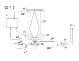
以下、図面を参照しながら本発明による実施の形態について説明する。図1は本発明による投影露光装置の概略的構成を示している。図1に示すように、例えば193nmの出力波長を持つパルス光を発振するArFエキシマレーザ光源1からほぼ平行光束としての出射されたレーザ光は、所定断面形状のレーザ光に整形するビーム整形光学系やビームエキスパンダなどからなるビームマッチングユニット2を通過して可変減光器3に入射する。可変減光器3は、露光量制御ユニット4からの指令に応じてパルスレーザ光の減光率を段階的にもしくは無段階に調節する。減光器3の射出光はビームスプリッタ5に入射し、その透過光は照明光学ユニット6に入射する。なお、照明光学系はチャンバ28に収容され、レーザ光源1はチャンバ28の外に設置されるから、チャンバ28にはレーザ光源1からのレーザ光を通過させる透過窓(不図示)が設けられている。
【0014】
また図1において、照明光学ユニット6には第1フライアイレンズ7が、照明光学ユニット8には第2フライアイレンズが設けられている。第1フライアイレンズ7の射出面近傍には2次光源としての面光源が形成される。第1フライアイレンズ7からの照明光は照明光学ユニット8に入射し、第2フライアイレンズ9の射出面近傍に3次光源としての面光源が形成される。
【0015】
第2フライアイレンズ9によって形成される面光源の位置にはタレット板10が配設されている。石英等の透明基板からなるタレット板10には、σ値を変更する開口絞りや変形照明用開口絞りが設けられ、投影光学系PLの解像力や焦点深度を向上させるためにいずれか一つが照明光路中の3次光源位置に挿入される。そのため、タレット板10はモータ10Aで回転駆動され、レチクルRのパターンの種類に応じて1つの開口絞りが選択されて照明光学系の光路中に挿入される。モータ10Aは主制御ユニット11からの指令で制御される。
【0016】
第2フライアイレンズ9による3次光源からの光束は、可変開口絞りを通過してビームスプリッタ12で2つの光路に分岐され、反射光はインテグレータセンサ(光電検出器)13に導かれて照明光の照度が検出される。検出された照度に応じた信号は露光量制御ユニット4に入力される。ビームスプリッタ12はその透過率は高いが、反射率は低く設定されている。一方、透過光は第3照明光学ユニット14により集光されて重畳的に照明視野絞りユニット(レチクルブラインド系)15を照明する。この照明視野絞りユニット15は第1照明光学ユニット6中の第1フライアイレンズ7の入射面および第2照明光学ユニット8中の第2フライアイレンズ9の入射面と共役な位置に配置されている。ここで、照明視野絞りユニット15上での照明領域は、第2フライアイレンズ9の各レンズエレメントの断面形状とほぼ相似形状となる。照明視野絞りユニット15の視野絞りの大きさは、主制御ユニット11からの指令により図示しない駆動機構により露光対象のショット領域に対応した開口に設定され、ウエハW上で本来のショット領域以外の領域に照明光が照射されるのを防止する。
【0017】
照明視野絞りユニット15を通過した照明光は第4照明光学ユニット16を通って反射ミラー17で反射された後、複数のレンズ等の屈折性光学素子で構成されるコンデンサ光学系である第5照明光学ユニット18で集光される。これにより、レチクルR上に形成された回路パターンがほぼ均一な照度分布で照明される。ここで、照明視野絞りユニット15中のレチクルブラインドとレチクルRのパターン面とは、第4および第5照明光学ユニット16,18に関してほぼ共役に配置されており、ブラインド開口によりレチクルR上の照明領域が規定される。
【0018】
そして投影光学系PLによってウエハW上にレチクルR上の回路パターンの像が形成され、ウエハW上に塗布されたレジストが感光して、ウエハW上に回路パターン像が転写される。
【0019】
レチクルRはレチクルホルダを介してレチクルステージRSに保持固定される。レチクルステージRSは、図1の紙面と直交する面内に沿って2次元的に移動するように図示しないベースに設けられている。レチクルステージRSにはミラーが設置され、レーザ干渉計からのレーザ光がミラーで反射されてレーザ干渉計に入射し、レーザ干渉計によりレチクルステージRSの位置が計測される。この干渉計とミラーの図示は省略した。この位置情報は主制御ユニット11に入力され、この位置情報に基づいて主制御ユニット11はレチクルステージ駆動用モータを駆動してレチクルRの位置を制御している。また、レチクルステージRSにはレチクル照度センサ31が設けられ、レチクルRに照射される照明光の照度が計測されて主制御ユニット11に入力される。
【0020】
ウエハWはウエハホルダを介してウエハステージWSに保持固定される。ウエハステージWSは、図1の紙面と直交する面内に沿って2次元的に移動するように設けられている。ウエハステージWSにはミラー(図示を省略)が設置され、レーザ干渉計19からのレーザ光がミラーで反射されてレーザ干渉計19に入射し、レーザ干渉計19によりウエハステージWSの位置が計測される。この位置情報は主制御ユニット11に入力され、この位置情報に基づいて主制御ユニット11はウエハステージ駆動系20を駆動してウエハWの位置を制御している。ウエハステージWS上にはウエハ照度センサ32が設けられ、ウエハWに照射される露光光の照度が検出される。このウエハ照度センサ32の検出信号は主制御ユニット11に入力される。レチクル照度センサ31の出力値をウエハ照度センサ32の出力値で除した値が投影光学系PLの透過率となる。
【0021】
次に、自動合焦系について図2も参照して説明する。自動合焦系は、ウエハステージWS上に設けられ、所定の開口パターン22aが形成されたフュデューシャルマーク22と、このフュデューシャルマーク22の開口パターン22aに露光光路から分岐された洗浄光を導く逆発光系21と、開口パターン22aを通過した洗浄光によりレチクルパターン面で形成されたパターン投影像の反射光を受光する光量検出器24と、投影光学系PLの下方に固定されてウエハW面の光軸方向の位置を検出する斜入射フォーカスセンサ26,27とを備える。光量検出器24と斜入射フォーカスセンサ27の検出信号は主制御系4に入力される。
【0022】
逆発光系21は、露光光路から分岐された洗浄光を通過遮断するシャッタ33と、光ファイバケーブル23と、ハーフミラ−25と、その他の光学系とを備え、ビームスプリッタ5から分岐された露光光は光ファイバケーブル23からハーフミラー25を介してフュデューシャルマーク22の開口パターン22aに導かれる。なお、ArF光などの短波長光は光ファイバケーブルでの減衰が大きいので、光ファイバケーブル23に代えてミラーを組合せた光学系を用い、さらに光路を窒素ガスで置換するのが好ましい。
【0023】
このような自動合焦系は次のようにして、ウエハステージの傾斜角度を調節するとともに、1ショットごとにウエハ表面にレチクルパターンを合焦させるようにする。ウエハを露光する前にシャッタ33を開いておく。これにより、露光用光源1からパルス光を射出させると、洗浄光がフュデューシャルーマーク22に導かれ、開口パターン22aを通過する逆発光像は投影光学系PLを通ってレチクルRに達し、レチクルパターン面に投影像が結像される。この投影像がレチクルパターン面で反射する光束は投影光学系PLを逆に進行してレチクルパターン面の投影光学系PLに関して共役な面に結像する。開口パターン22aの面が投影光学系PLに関してレチクルパターン面と共役な位置関係にあれば、レチクルパターン面での第1の投影像はピントがあった境界が明瞭なものとなる。またこの場合、第1の投影像の反射光による第2の投影像は、開口パターン22aの面上で結像してピントがあって境界が明瞭となる。第2の投影像は第1の投影像と同一形状、同一寸法、同一姿勢であるから、第2の投影像の光束の全てが開口パターン22aを通って光量検出器24に達し、受光量は最大となる。一方、開口パターン22aの面がレチクルパターン面の共役位置からずれている場合には、開口パターン22aの面上での第2の投影像はピントがずれて境界がボケたものとなる。その結果、第2の投影像は開口パターン22aからはみ出し、光量検出器24の受光量は低下する。
【0024】
このような原理を用いて、ウエハステージWSの複数の位置におけるZ軸方向の高さ位置の情報を検出する。すなわち、開口パターン22aをレチクルパターン面上の複数の位置に順番に位置決めし、各位置において光量検出器24の出力が最大となるようにする。こうして得られた高さ情報に基づいてウエハステージWSの傾斜角度が図示しない傾斜角度調節機構によって調整される。傾斜が調整された後、開口パターン22aを投影光学系PLの光軸に移動させ、再度、開口パターン22aの面が合焦位置となるようにウエハステージWSのZ軸高さ方向を調節する。そして、この状態で開口パターン22aの面を斜入射フォーカスセンサ26,27で検出し、この検出値、すなわち、フュデューシャルマーク22の面上でのビームスポット高さが原点として記憶される。その後ウエハステージWSの任意の位置に投影光学系PLの視野を走査した際には、斜入射フォーカスセンサ26,27における反射ビームスポットの高さにより試料の露光面高さが計測され、露光面高さが原点高さとなるように主制御ユニット11はウエハステージWSをZ軸方向に調節しながら露光が行なわれる。
【0025】
自動合焦系のフュデューシャルマーク22から射出される逆発光はアライメント系としても使用される。図3はレチクルRとウエハステージWSの位置決めのアライメント系を説明する図である。レチクルRには黒パターンであるレチクルマークRMが形成されている。このレチクルマークRMは開口パターン22aの像をレチクルパターン面に投影した投影像と同一形状、同一寸法のパターンである。フュデューシャルマーク22の開口パターン22aを透過した逆発光光は投影光学系PLを通ってレチクルRのパターン面に照射される。ウエハステージWSを移動させて開口パターン22aからの逆発光光の投影像を走査する。投影像がレチクルマークRMとちょうど重なり合うと、光量検出器34の受光量は最小となり光量信号も最小となる。このような手法によりレチクルRとウエハステージWSを位置合せできる。
【0026】
また、光量検出器34に代えてCCDのような撮像素子で開口パターン22aの投影像とレチクルマークRMの位置関係を撮像し、この画像を画像処理してアライメントするようにしてもよい。
【0027】
以上に構成される実施の形態の投影露光装置では、酸素による露光光の吸収を防ぐため、照明光学系を酸素の含有率を極めて小さく抑えた窒素ガスなどの不活性ガス雰囲気中に配設する。そのため、照明光学系のチャンバ28に不活性ガスを配管29aを介して供給する不活性ガス供給装置と、チャンバ28から汚染された不活性ガスを配管29bを介して排出する不活性ガス排出装置とが設けられる。また、投影光学系PLを構成する複数の光学部材間に形成される複数の空間にも窒素ガスなどの不活性ガスを供給し、汚染された不活性ガスを複数の空間から排出する。そのため、ガス供給装置は配管30aを介して投影光学系PLの内部へ乾燥した窒素などの不活性ガスを供給し、排出装置は投影光学系PLの内部の気体を配管30bを介して外部へ排出する。なお、不活性ガスとしては窒素に限ることなく、ヘリウム、アルゴン等の気体を用いることも可能である。
【0028】
チャンバ28や投影光学系PLの鏡筒の気密性が高い場合には、いったん大気と窒素を完全に置換した後は、その置換を頻繁に行なう必要はない。しかしながら、光路内に介在する硝材、コート材、接着剤、塗料、金属、セラミックなどの各種の物質から発生する水分子やハイドロカーボンなどが光学素子の表面に付着して透過率変動が起こるので、常時窒素ガスをチャンバ内や投影光学系の鏡筒内に流しつつ、ケミカルフィルタや静電フィルタによってチャンバ内や投影光学系の鏡筒内の不純物を除去するのが好ましい。
【0029】
次に本例における動作について説明する。まず、図1に示すように、乾燥した窒素等の不活性ガスをガス供給装置から配管29a,30aを介してチャンバ28と投影光学系PLの鏡筒内部に供給し、完全に充填された後、排出装置によりチャンバ28と投影光学系PLの鏡筒内部の気体を配管29a,30bを介して外部へ排出する。
【0030】
なお、上述したように、露光中もガス供給装置と排出装置を常時作動させ、チャンバ28や投影光学系PLの鏡筒内の光学素子間の雰囲気を常に乾燥清浄された状態に保持するのが好ましいが、露光動作に先立ってチャンバ28や投影光学系PLの鏡筒のレンズ室などの光学素子間に形成される空間の気体を清浄化した後は、供給装置と排出装置を停止させてもよい。
【0031】
次いで、不図示のレチクルローディング機構により、転写対象となるパターンが描画されたレチクルRをレチクルステージRSの上に搬送して載置する。このとき、そのレチクルRが所定の位置に設置されるように、不図示のレチクルアライメント系によりそのレチクルRの位置を計測し、その結果にしたがって、不図示のレチクル位置制御回路によってレチクルRの位置を所定の位置に設定する。
【0032】
レチクルRのパターンが転写されるウエハWの表面には感光材料であるレジストがあらかじめ塗布されており、その状態で不図示のウエハローディング機構によりウエハWが搬送されてウエハステージWS上に設置される。ウエハWはウエハステージWS上でアライメントされて保持固定される。
【0033】
露光作業を開始する前に、ウエハステージWS上に設けた照度センサ32を投影光学系PLの光軸上に移動して、インテグレータセンサ13の計測値L1と照度センサ32の計測値LWをサンプリングする。一方、レジスト材の感度特性などに応じてウエハ上での目標照度TLが設定される。インテグレータセンサ13は第1および第2フライアイレンズ7,9で均一化された露光光の照度に応じた検出信号LIを出力する。照度センサ32はウエハステージWS上の露光光の照度に応じた検出信号LWを出力する。インテグレータセンサ13の検出信号LIと照度センサWSの検出信号LWとの比(センサ32の出力LW/センサ13の出力LI)を算出し、この比LW/LIに所定の係数K1を乗じてゲインαを演算する。そして露光作業中は、インテグレータセンサ13の出力信号にゲインαが乗じられて推定実照度LPRが出力される。すなわち、推定実照度LPRは、露光開始時においてインテグレータセンサ13の計測値が100でウエハ上の照度が50であるとした場合、50/100の比率に所定の係数K1を乗じて求めたゲインαと、露光中のインテグレータセンサ13の出力信号とを乗じてウエハ上の照度を推定したものである。そして、推定実照度LPRが照度目標値TLになるように、主制御ユニット11からの指令にしたがって露光量制御ユニット4が光源1への印加電圧(充電電圧)を変更することで、レーザ光源1の出力が調節される。また、露光量制御ユニット4が減光器3の透過率(減光率)を調整してもよいし、あるいは光源1と減光器3の両方を制御してもよい。これにより、光源の劣化に伴う照度の低減が防止される。
【0034】
ウエハステージWS上に設置されたウエハWは第1回目のパターンの転写では、そのウエハW上にパターンは存在せず、ウエハステージWS上の所定の位置に、例えばウエハWの外径基準で定められる位置に設置される。その後、ウエハW上にパターンが転写される。この転写は、レチクルR上のパターンの一部を可変視野絞り(レチクルブラインド)15によって選択的に照明し、レチクルステージRSによってレチクルRをその可変視野絞り15によって規定される照明領域に対して相対移動し、それに同期しながらウエハWをウエハステージWSによって投影光学系PLに関してその照明領域と共役な投影領域に対して相対移動する、いわゆる走査型の転写(ステップアンドスキャン方式)である。あるいは、転写したいレチクルR上のパターン領域の全面を1度に全て照明して転写するステップアンドリピート方式でもよい。
【0035】
ウエハWに対する第2回目以降のパターンの転写の場合には、少なくともウエハW上にはパターンが存在するから、そのあらかじめ転写されたパターンに付設されるマークを不図示のウエハアライメント系により計測することによりウエハW上のそのパターンの位置を計測し、その結果にしたがって、ウエハW上に先に転写されたパターンに対して、これから転写するパターンが所定の位置関係になるように、レチクルステージRSやウエハステージWSの位置を制御する。
【0036】
このようなパターン露光中、露光光により投影光学系PLは光洗浄されるが、露光開始前は汚染物質が光学系の表面に付着していて透過率が低い値にあり、また、露光光の照射を停止すると雰囲気中に浮遊している汚染物質が光学系の表面に再付着して透過率が低下する。そのため、露光開始前にいわゆるパルスの空打ちにより光洗浄を行ない、光学系表面から汚染物質を除去して透過率を所定値以上に高めてから露光を開始する。また、この実施の形態では露光開始前に自動合焦系によりウエハステージWSの傾斜角度を調整するが、このとき、逆発光系21から照射されるパルス光により投影光学系PLは光洗浄される。この場合、パルス光は露光光とは逆方向にウエハステージWS側から進行するので、露光光により光洗浄される面とは逆の面にパルス光が照射される。したがって、レチクル側からの露光光では除去しきれない投影光学系PLのウエハ側の面に付着する汚染物質を除去することができる。
【0037】
ここで、露光前のパルス空打ちと並行して逆発光系21からも洗浄光を照射しながらウエハステージWSを走査すれば、投影光学系PLのウエハステージ側の面に照射される逆発光系21からの光でも光洗浄されるので、光洗浄時間が短縮できる。また、逆発光系21からの洗浄光を使用するので開口絞りの大きさや形状に影響を受けることなく、所定の光洗浄を行なうことができる。
【0038】
露光中や露光停止中に投影光学系PLの透過率を演算し、その透過率が所定値以下に低下したときに光洗浄を行なうようにしてもよい。演算結果の透過率が所定値以下の場合には、シャッタ33を開き、ウエハステージWSを移動してフュデューシャルマーク22を投影光学系PLの照射領域内で走査しながら、レーザ光源1からレーザ光を照射する。したがって、投影光学系PLが露光光と逆発光系からの光の双方で光洗浄され、露光光だけで光洗浄する場合に比べて光洗浄効率がよい。
【0039】
投影光学系PLの汚染ムラを測定し、汚染が進んでいる領域を逆発光で狙い打ちして光洗浄することができる。すなわち、ウエハステージWS上の照度センサ32を投影光学系PLの照明領域内で走査することにより、主制御ユニット11において、投影光学系PLの汚染状態を検出する。そして、汚染状態が悪い領域に逆発光系21からの照射光が照射されるようにウエハステージWSを移動させることにより、特定の箇所のみ光洗浄を行なって汚染ムラを解消できる。
【0040】
逆発光系21からの光で投影光学系PLを洗浄する場合、レチクルステージRS上にミラーを設置し、逆発光系21から照射される光をそのミラーで全反射させることにより光洗浄効率を高めることができる。
【0041】
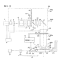
以上では、露光用レーザ光源1の射出光を洗浄用光学系に分岐して洗浄光を生成したが、露光光量が不足する場合には、洗浄用光源を用いるのが好ましい。図4はその場合の投影露光装置の一実施の形態を示す。図4に示すように、洗浄用光源51からの出射光はシャッタ33を介して光ファイバーケーブル23に入射される。洗浄用光源51は露光用レーザ光源1と同一のものでもよいが、光洗浄効果が期待できればその他の光源でもよく、たとえば、低圧水銀灯を使用できる。
【0042】
さらに以上では自動合焦系やアライメント系に使用する逆発光光を用いるようにしたが、この逆発光系とは別にウエハステージWS側から洗浄光を照射する光洗浄専用の光学系を用いてもよい。この場合、照明領域を大きくすることができ、開口パターン22aの走査時間よりも短い時間で洗浄できる。また、図1あるいは図2に示した逆発光系のNAは小さく、洗浄領域も極めて限られ、洗浄できない領域が残ってしまう。そこで、NAを大きくしたり、凹レンズなどにより光束を広げるレンズを用いてもよい。あるいは、微細な回折格子を介して洗浄光を投影光学系PLに入射させて、洗浄領域を広げてもよい。
【0043】
以上の実施の形態と請求項との対応において、レチクルRが原版を、逆発光系21が洗浄用光学系を、主制御ユニット11が汚染状態検出手段をそれぞれ構成する。
以上のように本実施の形態によれば、
(1)露光光の進行方向と反対の方向から入射する洗浄光で光学素子を光洗浄するようにしたので、露光光では洗浄し切れない感光基板側の汚れを洗浄することができる。
(2)洗浄光を露光光を分岐して生成すれば、専用の光源が不要となる、低コスト化を図ることができる。
(3)洗浄光を露光用光源とは別に設けた洗浄用光源で生成することにより、露光光の光量を落とすことなく大きな光量で洗浄することができる。
(4)露光光の進行方向と反対の方向から入射する洗浄光で光学素子を光洗浄するのと並行して、露光光の進行方向から入射する露光光で光学素子を光洗浄することにより、短時間で所定の透過率まで洗浄することができ、スループットが向上する。
(5)光学素子の汚染状態を検出し、その汚染状態に応じて洗浄光を走査すれば、局部的な汚染状態を除去することができる。
【0044】
【発明の効果】
以上のように本発明によれば、露光光の進行方向と反対の方向から入射する洗浄光で光学素子を光洗浄するようにしたので、露光光では洗浄し切れない感光基板側の汚れを洗浄することができる。
また、ステージから射出された洗浄光を投影光学系側に向けて照射しているので、露光光では洗浄し切れない感光基板側の汚れを洗浄することができる。
【図面の簡単な説明】
【図1】本発明による投影露光装置の一実施の形態の概略的構成を示す図
【図2】図1の自動合焦系の詳細図
【図3】図2の自動合焦系の逆発光光を用いるアライメント系を説明する図
【図4】洗浄用に専用の光源を用いた実施の形態を示す図
【図5】透過率変動を説明する図
【符号の説明】
1 ArFエキシマレーザ光源
4 露光量制御ユニット
11 主制御ユニット
13 インテグレータセンサ
21 逆発光系
24 光量検出器
31 レチクル照度センサ
32 ウエハ照度センサ
33 シャッタ
51 洗浄用光源
R レチクル
RS レチクルステージ
PL 投影光学系
W ウエハ
WS ウエハステージ[0001]
BACKGROUND OF THE INVENTION
The present invention includes, for example, a mask or a reticle (hereinafter referred to as a reticle) in a photolithography process for manufacturing a semiconductor element such as an LSI, an image pickup element such as a CCD, a liquid crystal display element, or a thin film magnetic head. The present invention relates to an optical element light cleaning method and a projection exposure apparatus for exposing a pattern of the original plate onto a photosensitive substrate such as a wafer.
[0002]
[Prior art]
Along with the high integration of semiconductor elements, projection exposure apparatuses used in photolithography processes important for manufacturing the semiconductor elements have also made rapid progress. The resolving power of the projection optical system mounted on the projection exposure apparatus is represented by the relationship of R = k × λ / NA, as is well known from the Rayleigh equation. Here, R is the resolution of the projection optical system, λ is the wavelength of light for exposure, NA is the numerical aperture of the projection optical system, and k is a constant determined by the process in addition to the resolution of the resist.
[0003]
In order to realize the necessary resolving power in the projection optical system corresponding to the high integration of semiconductor elements, as can be seen from the above equation, the exposure light source is shortened in wavelength and the numerical aperture of the projection optical system is increased. The so-called high NA efforts are continuing. In recent years, a krypton excimer laser (KrF excimer laser) having an output wavelength of 248 nm is used as an exposure light source, and an exposure apparatus having a projection optical system with a numerical aperture of 0.6 or more has been put into practical use. It is now possible to expose various patterns.
[0004]
In particular, recently, an argon fluoride excimer laser (ArF excimer laser) having an output wavelength of 193 nm has attracted attention as a light source following the krypton fluoride excimer laser. If an exposure apparatus using this argon fluoride excimer laser as an exposure light source can be realized, it is expected that microfabrication ranging from 0.18 μm to 0.13 μm will be possible, and vigorous research and development has been actively conducted. ing.
[0005]
In the wavelength region of the output wavelength (193 nm) of this argon fluoride excimer laser, materials that can be used as a lens from the viewpoint of transmittance, workability, etc. are synthetic quartz glass and calcium fluoride (fluorite). Therefore, as an optical material for this type of exposure apparatus, development of a material having sufficient transmittance and internal uniformity has continued. Synthetic quartz glass has an internal transmittance of 0.995 / cm or more, and calcium fluoride has reached a level at which internal absorption can be ignored.
[0006]
The anti-reflection coating material coated on the surface of the optical material has a very narrow selection range compared to the krypton fluoride excimer laser output wavelength (248 nm) wavelength range, greatly restricting design freedom. receive. However, the problem is being overcome by vigorous development efforts, and the loss on each lens surface has been realized to a level of 0.005 or less.
[0007]
[Problems to be solved by the invention]
In such a wavelength range shorter than the wavelength of the KrF excimer laser beam, moisture and organic substances adhere to the surface of the optical element constituting the optical system (illumination optical system, projection optical system) in the projection exposure apparatus. There is a problem that the transmittance of the liquid crystal decreases. This is because moisture, hydrocarbons, and organic matter generated from the gas in the space between the optical elements, or from the inner wall of the lens barrel that supports the optical system, the adhesive, and the like adhere to the surface of the optical system. .
[0008]
FIG. 5 shows the time-varying characteristics of the transmittance of the optical system. While continuously emitting pulsed laser light from the laser light source, the illuminance of the exposure light between the laser light source and the reticle and the exposure light on the wafer are shown. Illuminance is measured at predetermined time intervals, and the optical system transmittance, which is the ratio of the two illuminances, is calculated for each measurement time. As can be seen from FIG. 5, the transmittance gradually increases immediately after the start of laser light irradiation, and when a certain amount of time elapses, the state is almost saturated. Such variation in transmittance occurs because variation in internal characteristics of the glass material and moisture and organic substances adhering to the optical system surface are removed from the optical system surface by laser irradiation.
[0009]
Therefore, during the exposure operation in the projection exposure apparatus, that is, the reticle is illuminated with the exposure light from the illumination optical system, and at least a part of the device pattern on the reticle is projected onto the photosensitive substrate by the projection optical system. When the pattern image is sequentially transferred onto the photosensitive substrate by the step-and-repeat method or the step-and-scan method, the transmittance of the illumination optical system and the projection optical system gradually increases. However, this increase in transmittance is a temporary cleaning effect, and an optical system in which the surface of the optical element is activated by exposure to exposure light tends to adhere to surrounding moisture and organic matter when the irradiation is stopped. To do. Therefore, when the exposure light exposure (exposure operation) is stopped for a long time or for a long time, the transmittance is almost saturated by irradiating the exposure laser light for a predetermined time before starting the exposure and cleaning it as necessary. It is conceivable that the exposure operation is started after that, but it takes time to clean up to a predetermined transmittance. Further, when the cleaning light is incident from the same direction as the exposure light, the light cleaning of the exit surface is insufficient as compared with the incident surface of the cleaning light.
[0010]
An object of the present invention is to provide an optical element light cleaning method and a projection exposure apparatus in which the surface of the optical element on the side of the photosensitive substrate is sufficiently optically cleaned.
[0011]
[Means for Solving the Problems]
The embodiment will be described with reference to FIGS.
(1) The invention of
(2) The invention of claim 2 is the light cleaning method of
(3) The invention of
(4) The invention of
(5) The invention of claim 5 is applied to a projection exposure apparatus provided with an optical element that illuminates an original R on which a predetermined pattern is formed with exposure light, and projects an image of the illuminated pattern onto the photosensitive substrate W. Is done. The above object is achieved by providing the optical cleaning
(6) The invention of claim 6 comprises the branching optical element 5 for guiding the illumination light emitted from the
(7) The invention of claim 7 is the exposure apparatus according to claim 5, further comprising a light
(8) The invention according to claim 8 is the projection exposure apparatus according to any one of claims 5 to 7, further comprising a contamination state detection means for detecting a contamination state of the optical element, and cleaning according to the detected contamination state. The
(9) The optical cleaning method according to the invention of claim 9 illuminates an original R on which a predetermined pattern is formed with exposure light, and projects an image of the illuminated pattern onto the photosensitive substrate W; In an optical cleaning method used in an exposure apparatus including a stage WS including a
(10) The invention of
(11) The invention of
(12) According to the invention of
(13) A projection exposure apparatus according to a thirteenth aspect of the present invention includes a projection optical system PL that illuminates an original R on which a predetermined pattern is formed with exposure light, and projects an image of the illuminated pattern onto the photosensitive substrate W; In a projection exposure apparatus that includes a stage WS that includes a
(14) The invention according to claim 14 is the exposure apparatus according to
(15) The invention of claim 15 is a claim.13Or14In this exposure apparatus, the stage WS has an
[0012]
Although the present invention has been described with reference to the drawings of the embodiments in the section for solving the above problems, the present invention is not limited to the embodiments.
[0013]
DETAILED DESCRIPTION OF THE INVENTION
Embodiments according to the present invention will be described below with reference to the drawings. FIG. 1 shows a schematic configuration of a projection exposure apparatus according to the present invention. As shown in FIG. 1, for example, a laser beam emitted from an ArF excimer
[0014]
In FIG. 1, the illumination optical unit 6 is provided with a first fly-eye lens 7, and the illumination optical unit 8 is provided with a second fly-eye lens. A surface light source as a secondary light source is formed near the exit surface of the first fly-eye lens 7. Illumination light from the first fly-eye lens 7 enters the illumination optical unit 8, and a surface light source as a tertiary light source is formed near the exit surface of the second fly-eye lens 9.
[0015]
A
[0016]
The light beam from the tertiary light source by the second fly-eye lens 9 passes through the variable aperture stop and is branched into two optical paths by the
[0017]
The illumination light that has passed through the illumination field stop unit 15 is reflected by the
[0018]
Then, an image of the circuit pattern on the reticle R is formed on the wafer W by the projection optical system PL, the resist applied on the wafer W is exposed, and the circuit pattern image is transferred onto the wafer W.
[0019]
Reticle R is held and fixed to reticle stage RS via a reticle holder. Reticle stage RS is provided on a base (not shown) so as to move two-dimensionally along a plane perpendicular to the paper surface of FIG. The reticle stage RS is provided with a mirror, and the laser light from the laser interferometer is reflected by the mirror and enters the laser interferometer, and the position of the reticle stage RS is measured by the laser interferometer. The interferometer and mirror are not shown. This position information is input to the
[0020]
Wafer W is held and fixed to wafer stage WS via a wafer holder. The wafer stage WS is provided so as to move two-dimensionally along a plane orthogonal to the paper surface of FIG. The wafer stage WS is provided with a mirror (not shown), the laser beam from the
[0021]
Next, the automatic focusing system will be described with reference to FIG. The automatic focusing system is provided on the wafer stage WS, and the
[0022]
The reverse
[0023]
Such an automatic focusing system adjusts the tilt angle of the wafer stage as follows, and focuses the reticle pattern on the wafer surface for each shot. The
[0024]
Using such a principle, information on height positions in the Z-axis direction at a plurality of positions of the wafer stage WS is detected. That is, the
[0025]
The reverse emission emitted from the automatic focus type
[0026]
Further, the positional relationship between the projected image of the
[0027]
In the projection exposure apparatus having the above-described configuration, the illumination optical system is disposed in an inert gas atmosphere such as nitrogen gas in which the oxygen content is extremely low in order to prevent exposure light from being absorbed by oxygen. . Therefore, an inert gas supply device that supplies the inert gas to the
[0028]
When the airtightness of the
[0029]
Next, the operation in this example will be described. First, as shown in FIG. 1, after an inert gas such as dry nitrogen is supplied from the gas supply device through the
[0030]
As described above, the gas supply device and the discharge device are always operated even during exposure, and the atmosphere between the optical elements in the
[0031]
Next, the reticle R on which the pattern to be transferred is drawn is transported and placed on the reticle stage RS by a reticle loading mechanism (not shown). At this time, the position of the reticle R is measured by a reticle alignment system (not shown) so that the reticle R is placed at a predetermined position, and the position of the reticle R is detected by a reticle position control circuit (not shown) according to the result. Is set to a predetermined position.
[0032]
A resist, which is a photosensitive material, is applied in advance to the surface of the wafer W to which the pattern of the reticle R is transferred. In this state, the wafer W is transported by a wafer loading mechanism (not shown) and placed on the wafer stage WS. . The wafer W is aligned and held and fixed on the wafer stage WS.
[0033]
Before the exposure operation is started, the
[0034]
The wafer W placed on the wafer stage WS has no pattern on the wafer W in the first pattern transfer, and is determined at a predetermined position on the wafer stage WS, for example, based on the outer diameter reference of the wafer W. It is installed at the position where Thereafter, the pattern is transferred onto the wafer W. In this transfer, a part of the pattern on the reticle R is selectively illuminated by a variable field stop (reticle blind) 15, and the reticle R is relative to an illumination region defined by the variable field stop 15 by a reticle stage RS. This is a so-called scanning transfer (step-and-scan method) in which the wafer W moves relative to the projection area conjugate with the illumination area with respect to the projection optical system PL by the wafer stage WS while moving. Alternatively, a step-and-repeat method may be used in which the entire pattern area on the reticle R to be transferred is illuminated and transferred at once.
[0035]
In the case of the second and subsequent transfer of the pattern to the wafer W, since the pattern exists at least on the wafer W, the mark attached to the previously transferred pattern is measured by a wafer alignment system (not shown). Is used to measure the position of the pattern on the wafer W, and according to the result, the reticle stage RS or the like is used so that the pattern transferred from the pattern transferred on the wafer W has a predetermined positional relationship. The position of the wafer stage WS is controlled.
[0036]
During such pattern exposure, the projection optical system PL is optically washed by the exposure light, but before the start of exposure, contaminants adhere to the surface of the optical system and the transmittance is low, and the exposure light When the irradiation is stopped, contaminants floating in the atmosphere reattach to the surface of the optical system and the transmittance is reduced. Therefore, light cleaning is performed by so-called pulse blanking before the start of exposure, and contaminants are removed from the optical system surface to increase the transmittance to a predetermined value or higher, and then exposure is started. In this embodiment, the tilt angle of the wafer stage WS is adjusted by an automatic focusing system before the start of exposure. At this time, the projection optical system PL is optically washed by the pulsed light emitted from the reverse
[0037]
Here, if the wafer stage WS is scanned while irradiating the cleaning light from the reverse
[0038]
The light transmittance may be calculated when the transmittance of the projection optical system PL is calculated during exposure or when the exposure is stopped, and the transmittance decreases below a predetermined value. When the transmittance of the calculation result is less than or equal to a predetermined value, the
[0039]
The unevenness of contamination of the projection optical system PL can be measured, and the region where the contamination is advanced can be aimed at by reverse light emission to be washed with light. That is, the
[0040]
When the projection optical system PL is cleaned with the light from the reverse
[0041]
In the above, the emission light from the exposure
[0042]
In the above, the reverse emission light used for the automatic focusing system and alignment system is used. However, in addition to this reverse emission system, an optical system dedicated to optical cleaning that irradiates cleaning light from the wafer stage WS side may be used. Good. In this case, the illumination area can be enlarged and cleaning can be performed in a time shorter than the scanning time of the
[0043]
In correspondence with the above embodiments and claims, the reticle R constitutes an original, the reverse
As described above, according to the present embodiment,
(1) Since the optical element is optically cleaned with the cleaning light incident from the direction opposite to the traveling direction of the exposure light, the stain on the photosensitive substrate side that cannot be cleaned with the exposure light can be cleaned.
(2) If the cleaning light is generated by branching the exposure light, a dedicated light source is not required, and the cost can be reduced.
(3) By generating the cleaning light with a cleaning light source provided separately from the exposure light source, it is possible to perform cleaning with a large amount of light without reducing the amount of exposure light.
(4) By optically cleaning the optical element with exposure light incident from the traveling direction of exposure light, in parallel with optical cleaning of the optical element with cleaning light incident from a direction opposite to the traveling direction of exposure light, A predetermined transmittance can be washed in a short time, and the throughput is improved.
(5) If the contamination state of the optical element is detected and the cleaning light is scanned according to the contamination state, the local contamination state can be removed.
[0044]
【The invention's effect】
As described above, according to the present invention,,Since the optical element is optically cleaned with the cleaning light incident from the direction opposite to the traveling direction of the exposure light, the stain on the photosensitive substrate side that cannot be cleaned with the exposure light can be cleaned.
Further, since the cleaning light emitted from the stage is irradiated toward the projection optical system side, the stain on the photosensitive substrate side that cannot be completely cleaned by the exposure light can be cleaned.
[Brief description of the drawings]
FIG. 1 is a diagram showing a schematic configuration of an embodiment of a projection exposure apparatus according to the present invention.
FIG. 2 is a detailed view of the automatic focusing system in FIG.
3 is a diagram for explaining an alignment system using reverse emission light of the automatic focusing system in FIG. 2;
FIG. 4 is a view showing an embodiment using a dedicated light source for cleaning.
FIG. 5 is a diagram for explaining transmittance variation
[Explanation of symbols]
1 ArF excimer laser light source
4 Exposure control unit
11 Main control unit
13 Integrator sensor
21 Reverse emission system
24 Light intensity detector
31 Reticle illuminance sensor
32 Wafer illumination sensor
33 Shutter
51 Light source for cleaning
R reticle
RS reticle stage
PL projection optical system
W wafer
WS Wafer stage
Claims (15)
前記露光光の進行方向と反対の方向から入射する洗浄光で前記光学素子を光洗浄することを特徴とする光学素子光洗浄方法。In an optical element light cleaning method for a projection exposure apparatus, which includes an optical element that illuminates an original plate on which a predetermined pattern is formed with exposure light, and projects an image of the illuminated pattern onto a photosensitive substrate.
An optical element light cleaning method, wherein the optical element is optically cleaned with cleaning light incident from a direction opposite to a traveling direction of the exposure light.
前記露光光の進行方向と反対の方向から洗浄光を前記光学素子に射出する光洗浄光学系を備えることを特徴とする投影露光装置。In a projection exposure apparatus that includes an optical element that illuminates an original on which a predetermined pattern is formed with exposure light, and projects an image of the illuminated pattern onto a photosensitive substrate.
A projection exposure apparatus comprising: a light cleaning optical system that emits cleaning light to the optical element from a direction opposite to a traveling direction of the exposure light.
前記ステージから射出された洗浄光を前記投影光学系側に向けて照射することを特徴とする光洗浄方法。A projection optical system that illuminates an original on which a predetermined pattern is formed with exposure light, projects an image of the illuminated pattern onto a photosensitive substrate, and a sensor that detects the illuminance of the exposure light that has passed through the projection optical system In an optical cleaning method used for an exposure apparatus including a stage including:
An optical cleaning method comprising irradiating the cleaning light emitted from the stage toward the projection optical system side.
前記ステージに設けられ、前記投影光学系側に洗浄光を射出する光洗浄光学系を備えることを特徴とする投影露光装置。A projection optical system that illuminates an original on which a predetermined pattern is formed with exposure light, projects an image of the illuminated pattern onto a photosensitive substrate, and a sensor that detects the illuminance of the exposure light that has passed through the projection optical system A projection exposure apparatus comprising a stage comprising:
A projection exposure apparatus comprising: a light cleaning optical system that is provided on the stage and emits cleaning light to the projection optical system side.
Priority Applications (1)
| Application Number | Priority Date | Filing Date | Title |
|---|---|---|---|
| JP02730198A JP4066083B2 (en) | 1998-02-09 | 1998-02-09 | Optical element light cleaning method and projection exposure apparatus |
Applications Claiming Priority (1)
| Application Number | Priority Date | Filing Date | Title |
|---|---|---|---|
| JP02730198A JP4066083B2 (en) | 1998-02-09 | 1998-02-09 | Optical element light cleaning method and projection exposure apparatus |
Publications (2)
| Publication Number | Publication Date |
|---|---|
| JPH11233402A JPH11233402A (en) | 1999-08-27 |
| JP4066083B2 true JP4066083B2 (en) | 2008-03-26 |
Family
ID=12217278
Family Applications (1)
| Application Number | Title | Priority Date | Filing Date |
|---|---|---|---|
| JP02730198A Expired - Fee Related JP4066083B2 (en) | 1998-02-09 | 1998-02-09 | Optical element light cleaning method and projection exposure apparatus |
Country Status (1)
| Country | Link |
|---|---|
| JP (1) | JP4066083B2 (en) |
Families Citing this family (4)
| Publication number | Priority date | Publication date | Assignee | Title |
|---|---|---|---|---|
| JP2003320329A (en) * | 2002-05-07 | 2003-11-11 | Honda Electronic Co Ltd | Ultrasonic cleaning apparatus |
| WO2005114711A1 (en) * | 2004-05-21 | 2005-12-01 | Jsr Corporation | Liquid for immersion exposure and immersion exposure method |
| JP2007027631A (en) * | 2005-07-21 | 2007-02-01 | Nikon Corp | Exposure method, exposure apparatus, and device manufacturing method |
| JP5025236B2 (en) * | 2006-11-29 | 2012-09-12 | キヤノン株式会社 | Exposure apparatus and method, and device manufacturing method |
-
1998
- 1998-02-09 JP JP02730198A patent/JP4066083B2/en not_active Expired - Fee Related
Also Published As
| Publication number | Publication date |
|---|---|
| JPH11233402A (en) | 1999-08-27 |
Similar Documents
| Publication | Publication Date | Title |
|---|---|---|
| JP4534260B2 (en) | Exposure method, exposure apparatus, manufacturing method thereof, and optical cleaning method | |
| JP5055310B2 (en) | Lithographic apparatus, radiation system, contaminant trap, device manufacturing method, and method of capturing contaminant in a contaminant trap | |
| US6268904B1 (en) | Optical exposure apparatus and photo-cleaning method | |
| TWI485532B (en) | Radiation system and lithographic apparatus comprising the same | |
| US20040227102A1 (en) | Method and device for measuring contamination of a surface of a component of a lithographic apparatus | |
| EP0874283B1 (en) | Optical exposure apparatus and photo-cleaning method | |
| KR20030076238A (en) | Euv-transparent interface structure | |
| JP3996135B2 (en) | Lithographic apparatus and device manufacturing method | |
| JPH11283903A (en) | Projection optical system inspection device and projection aligner provided with the device | |
| KR100718744B1 (en) | Radiation Detector | |
| JP4990944B2 (en) | Lithographic apparatus and method | |
| JP2001345245A (en) | Method and device for exposure and method of manufacturing device | |
| WO1999005710A1 (en) | Projection aligner, projection exposure method, optical cleaning method and method of fabricating semiconductor device | |
| JPH1078668A (en) | Inspection device | |
| JP4066083B2 (en) | Optical element light cleaning method and projection exposure apparatus | |
| WO2000055890A1 (en) | Exposure system and aberration measurement method for its projection optical system, and production method for device | |
| JP2009295981A (en) | Particle detection on patterning device with arbitrary pattern | |
| JP2005101314A5 (en) | ||
| JP4268364B2 (en) | Lithographic apparatus, device manufacturing method, and device manufactured thereby | |
| JP4029200B2 (en) | Projection exposure apparatus, projection exposure method, optical cleaning method, and semiconductor device manufacturing method | |
| JP2010056361A (en) | Exposure system and exposure method | |
| JPH10335235A (en) | Aligner, optical cleaning method thereof and manufacture of semiconductor device | |
| JP2006303270A (en) | Aligner | |
| JPH11191525A (en) | Projection aligner | |
| TW200842505A (en) | Lithographic apparatus and method |
Legal Events
| Date | Code | Title | Description |
|---|---|---|---|
| A621 | Written request for application examination |
Free format text: JAPANESE INTERMEDIATE CODE: A621 Effective date: 20050208 |
|
| A521 | Written amendment |
Free format text: JAPANESE INTERMEDIATE CODE: A523 Effective date: 20060428 |
|
| A977 | Report on retrieval |
Free format text: JAPANESE INTERMEDIATE CODE: A971007 Effective date: 20061026 |
|
| A131 | Notification of reasons for refusal |
Free format text: JAPANESE INTERMEDIATE CODE: A131 Effective date: 20071009 |
|
| A521 | Written amendment |
Free format text: JAPANESE INTERMEDIATE CODE: A523 Effective date: 20071115 |
|
| TRDD | Decision of grant or rejection written | ||
| A01 | Written decision to grant a patent or to grant a registration (utility model) |
Free format text: JAPANESE INTERMEDIATE CODE: A01 Effective date: 20071211 |
|
| A61 | First payment of annual fees (during grant procedure) |
Free format text: JAPANESE INTERMEDIATE CODE: A61 Effective date: 20071224 |
|
| FPAY | Renewal fee payment (event date is renewal date of database) |
Free format text: PAYMENT UNTIL: 20110118 Year of fee payment: 3 |
|
| R150 | Certificate of patent or registration of utility model |
Free format text: JAPANESE INTERMEDIATE CODE: R150 |
|
| LAPS | Cancellation because of no payment of annual fees |