JP4064550B2 - Programmable and spatially light-modulated microscope and microscope method - Google Patents
Programmable and spatially light-modulated microscope and microscope method Download PDFInfo
- Publication number
- JP4064550B2 JP4064550B2 JP30100398A JP30100398A JP4064550B2 JP 4064550 B2 JP4064550 B2 JP 4064550B2 JP 30100398 A JP30100398 A JP 30100398A JP 30100398 A JP30100398 A JP 30100398A JP 4064550 B2 JP4064550 B2 JP 4064550B2
- Authority
- JP
- Japan
- Prior art keywords
- image
- confocal
- light
- detector
- sequence
- Prior art date
- Legal status (The legal status is an assumption and is not a legal conclusion. Google has not performed a legal analysis and makes no representation as to the accuracy of the status listed.)
- Expired - Lifetime
Links
- 238000000034 method Methods 0.000 title claims abstract description 40
- 238000001514 detection method Methods 0.000 claims abstract description 33
- 238000005286 illumination Methods 0.000 claims abstract description 27
- 238000012634 optical imaging Methods 0.000 claims abstract description 10
- 238000010191 image analysis Methods 0.000 claims abstract 3
- 230000003287 optical effect Effects 0.000 claims description 26
- 238000004422 calculation algorithm Methods 0.000 claims description 13
- 238000003384 imaging method Methods 0.000 claims description 8
- 238000005259 measurement Methods 0.000 claims description 8
- 239000011159 matrix material Substances 0.000 claims description 6
- 238000004458 analytical method Methods 0.000 claims description 5
- 239000000126 substance Substances 0.000 claims description 5
- 230000036962 time dependent Effects 0.000 claims description 5
- 238000006552 photochemical reaction Methods 0.000 claims description 4
- 230000005540 biological transmission Effects 0.000 claims description 3
- 239000007795 chemical reaction product Substances 0.000 claims description 3
- 238000012252 genetic analysis Methods 0.000 claims description 3
- 238000007689 inspection Methods 0.000 claims description 3
- 230000013011 mating Effects 0.000 claims description 3
- 239000004065 semiconductor Substances 0.000 claims description 3
- 230000009897 systematic effect Effects 0.000 claims description 3
- 108091081062 Repeated sequence (DNA) Proteins 0.000 claims description 2
- 230000000977 initiatory effect Effects 0.000 claims description 2
- 238000011835 investigation Methods 0.000 claims description 2
- 238000000386 microscopy Methods 0.000 claims description 2
- 238000012544 monitoring process Methods 0.000 claims description 2
- 239000000758 substrate Substances 0.000 claims description 2
- 238000001069 Raman spectroscopy Methods 0.000 claims 1
- 238000003491 array Methods 0.000 claims 1
- 238000011138 biotechnological process Methods 0.000 claims 1
- 125000004122 cyclic group Chemical group 0.000 claims 1
- 230000010287 polarization Effects 0.000 claims 1
- 230000003252 repetitive effect Effects 0.000 claims 1
- 238000010586 diagram Methods 0.000 description 10
- 230000000875 corresponding effect Effects 0.000 description 8
- 239000000523 sample Substances 0.000 description 7
- 230000004044 response Effects 0.000 description 6
- 230000011218 segmentation Effects 0.000 description 6
- 238000004088 simulation Methods 0.000 description 6
- 230000010354 integration Effects 0.000 description 5
- 238000012545 processing Methods 0.000 description 5
- 230000015572 biosynthetic process Effects 0.000 description 3
- 230000005855 radiation Effects 0.000 description 3
- 238000012163 sequencing technique Methods 0.000 description 3
- 230000001629 suppression Effects 0.000 description 3
- 239000013598 vector Substances 0.000 description 3
- 238000010226 confocal imaging Methods 0.000 description 2
- 230000001276 controlling effect Effects 0.000 description 2
- 238000012937 correction Methods 0.000 description 2
- 230000000694 effects Effects 0.000 description 2
- 230000005284 excitation Effects 0.000 description 2
- 239000004973 liquid crystal related substance Substances 0.000 description 2
- 238000012805 post-processing Methods 0.000 description 2
- 238000011084 recovery Methods 0.000 description 2
- 230000035945 sensitivity Effects 0.000 description 2
- 108091026890 Coding region Proteins 0.000 description 1
- 108091028043 Nucleic acid sequence Proteins 0.000 description 1
- BQCADISMDOOEFD-UHFFFAOYSA-N Silver Chemical compound [Ag] BQCADISMDOOEFD-UHFFFAOYSA-N 0.000 description 1
- 230000002411 adverse Effects 0.000 description 1
- 230000003190 augmentative effect Effects 0.000 description 1
- 239000012472 biological sample Substances 0.000 description 1
- 238000004061 bleaching Methods 0.000 description 1
- 238000004364 calculation method Methods 0.000 description 1
- 238000006243 chemical reaction Methods 0.000 description 1
- 238000012790 confirmation Methods 0.000 description 1
- 230000002596 correlated effect Effects 0.000 description 1
- 230000001419 dependent effect Effects 0.000 description 1
- 238000009795 derivation Methods 0.000 description 1
- 230000023077 detection of light stimulus Effects 0.000 description 1
- 238000006073 displacement reaction Methods 0.000 description 1
- 230000009977 dual effect Effects 0.000 description 1
- 238000005516 engineering process Methods 0.000 description 1
- 238000002474 experimental method Methods 0.000 description 1
- 238000002073 fluorescence micrograph Methods 0.000 description 1
- 230000012447 hatching Effects 0.000 description 1
- RVRCFVVLDHTFFA-UHFFFAOYSA-N heptasodium;tungsten;nonatriacontahydrate Chemical compound O.O.O.O.O.O.O.O.O.O.O.O.O.O.O.O.O.O.O.O.O.O.O.O.O.O.O.O.O.O.O.O.O.O.O.O.O.O.O.[Na+].[Na+].[Na+].[Na+].[Na+].[Na+].[Na+].[W].[W].[W].[W].[W].[W].[W].[W].[W].[W].[W] RVRCFVVLDHTFFA-UHFFFAOYSA-N 0.000 description 1
- 238000001727 in vivo Methods 0.000 description 1
- 230000000670 limiting effect Effects 0.000 description 1
- 238000013507 mapping Methods 0.000 description 1
- 239000000463 material Substances 0.000 description 1
- 238000001000 micrograph Methods 0.000 description 1
- 230000000737 periodic effect Effects 0.000 description 1
- 230000008832 photodamage Effects 0.000 description 1
- 239000000047 product Substances 0.000 description 1
- 238000001243 protein synthesis Methods 0.000 description 1
- 230000002829 reductive effect Effects 0.000 description 1
- 230000002441 reversible effect Effects 0.000 description 1
- 238000005070 sampling Methods 0.000 description 1
- 238000000926 separation method Methods 0.000 description 1
- 229910052709 silver Inorganic materials 0.000 description 1
- 239000004332 silver Substances 0.000 description 1
- 230000003595 spectral effect Effects 0.000 description 1
- 238000001228 spectrum Methods 0.000 description 1
- 238000003786 synthesis reaction Methods 0.000 description 1
- 230000002123 temporal effect Effects 0.000 description 1
- 230000014616 translation Effects 0.000 description 1
Images


Classifications
-
- G—PHYSICS
- G02—OPTICS
- G02B—OPTICAL ELEMENTS, SYSTEMS OR APPARATUS
- G02B21/00—Microscopes
- G02B21/0004—Microscopes specially adapted for specific applications
- G02B21/002—Scanning microscopes
- G02B21/0024—Confocal scanning microscopes (CSOMs) or confocal "macroscopes"; Accessories which are not restricted to use with CSOMs, e.g. sample holders
- G02B21/008—Details of detection or image processing, including general computer control
- G02B21/0084—Details of detection or image processing, including general computer control time-scale detection, e.g. strobed, ultra-fast, heterodyne detection
-
- G—PHYSICS
- G02—OPTICS
- G02B—OPTICAL ELEMENTS, SYSTEMS OR APPARATUS
- G02B21/00—Microscopes
- G02B21/0004—Microscopes specially adapted for specific applications
- G02B21/002—Scanning microscopes
- G02B21/0024—Confocal scanning microscopes (CSOMs) or confocal "macroscopes"; Accessories which are not restricted to use with CSOMs, e.g. sample holders
- G02B21/0032—Optical details of illumination, e.g. light-sources, pinholes, beam splitters, slits, fibers
-
- G—PHYSICS
- G02—OPTICS
- G02B—OPTICAL ELEMENTS, SYSTEMS OR APPARATUS
- G02B21/00—Microscopes
- G02B21/0004—Microscopes specially adapted for specific applications
- G02B21/002—Scanning microscopes
- G02B21/0024—Confocal scanning microscopes (CSOMs) or confocal "macroscopes"; Accessories which are not restricted to use with CSOMs, e.g. sample holders
- G02B21/0036—Scanning details, e.g. scanning stages
- G02B21/004—Scanning details, e.g. scanning stages fixed arrays, e.g. switchable aperture arrays
-
- G—PHYSICS
- G02—OPTICS
- G02B—OPTICAL ELEMENTS, SYSTEMS OR APPARATUS
- G02B21/00—Microscopes
- G02B21/0004—Microscopes specially adapted for specific applications
- G02B21/002—Scanning microscopes
- G02B21/0024—Confocal scanning microscopes (CSOMs) or confocal "macroscopes"; Accessories which are not restricted to use with CSOMs, e.g. sample holders
- G02B21/0036—Scanning details, e.g. scanning stages
- G02B21/0048—Scanning details, e.g. scanning stages scanning mirrors, e.g. rotating or galvanomirrors, MEMS mirrors
-
- G—PHYSICS
- G02—OPTICS
- G02B—OPTICAL ELEMENTS, SYSTEMS OR APPARATUS
- G02B21/00—Microscopes
- G02B21/0004—Microscopes specially adapted for specific applications
- G02B21/002—Scanning microscopes
- G02B21/0024—Confocal scanning microscopes (CSOMs) or confocal "macroscopes"; Accessories which are not restricted to use with CSOMs, e.g. sample holders
- G02B21/0052—Optical details of the image generation
- G02B21/0076—Optical details of the image generation arrangements using fluorescence or luminescence
-
- G—PHYSICS
- G02—OPTICS
- G02B—OPTICAL ELEMENTS, SYSTEMS OR APPARATUS
- G02B21/00—Microscopes
- G02B21/0004—Microscopes specially adapted for specific applications
- G02B21/002—Scanning microscopes
- G02B21/0024—Confocal scanning microscopes (CSOMs) or confocal "macroscopes"; Accessories which are not restricted to use with CSOMs, e.g. sample holders
- G02B21/008—Details of detection or image processing, including general computer control
-
- G—PHYSICS
- G02—OPTICS
- G02B—OPTICAL ELEMENTS, SYSTEMS OR APPARATUS
- G02B26/00—Optical devices or arrangements for the control of light using movable or deformable optical elements
- G02B26/08—Optical devices or arrangements for the control of light using movable or deformable optical elements for controlling the direction of light
- G02B26/0816—Optical devices or arrangements for the control of light using movable or deformable optical elements for controlling the direction of light by means of one or more reflecting elements
- G02B26/0833—Optical devices or arrangements for the control of light using movable or deformable optical elements for controlling the direction of light by means of one or more reflecting elements the reflecting element being a micromechanical device, e.g. a MEMS mirror, DMD
- G02B26/0841—Optical devices or arrangements for the control of light using movable or deformable optical elements for controlling the direction of light by means of one or more reflecting elements the reflecting element being a micromechanical device, e.g. a MEMS mirror, DMD the reflecting element being moved or deformed by electrostatic means
Abstract
Description
【0001】
【発明の属する技術分野】
本発明は、共焦点点顕微鏡、特にプログラム可能であり空間的に光変調されたまたはプログラム可能なアレイ顕微鏡と、照射および/または検出のために自由にプログラム可能なパターンを使用する顕微鏡方法に関する。
【0002】
【従来の技術】
ポイント走査システムに基づいた照射および検出開口の共役対を有する共焦点点顕微鏡は、直接光区分により極微物体を調査するように極微物体をイメージする有用な器具である。ディスクリートな開口スポットは顕微鏡の対物平面で照射され、そこから反射された光または蛍光性の光が画像平面の共役検出開口を通じて観察される。機械的に変形された開口ディスク(いわゆる複数の開口を有するニコウの円板)を有する走査システム、またはレーザビームで物体を走査するように構成された回転ミラーを有する走査システムに基づいた共焦点顕微鏡(共焦点レーザ走査顕微鏡、CSLM)が通常使用されている。
【0003】
両走査システムはある制限を有する。開口ディスクは特に照射フィールドに関する制限、劣化したコントラストおよび高い強度損失を有する。ピンホール間の間隔が共焦点効果を維持するだけの大きさでなければならないので、典型的にディスクの3%に満たない程度が透過性である。一方、CSLMの走査ミラーは逐次的な1つの点のデータ獲得により低いデューティサイクルを生じる。
【0004】
強度損失の問題は開口補正顕微鏡の導入により発生し、このことはR. JuskaitisとT. Wilson による“Nature”(383 巻、1996年、 804〜806 頁)と、T. Wilson とR. Juskaitisによる“Optics Letters”(21巻、1996年、1879〜1881頁)に記載されている。図9で概略して示されているようなこのような顕微鏡は、試験体照射のために光源とプログラム可能な開口マスクとの組合わせにより形成される多点光源を使用している。試験体により反射される光の検出は、同一の開口マスクを通じてカメラにより行われる。開口マスクは、アドレス可能な画素のアレイにより形成される高速度の空間的光変調器または固定して変調コードが付けられている回転ディスクである。
【0005】
マスクは補正されていない開口と閉塞のパターンを有し、ディスクの透過性を約50%まで増加する。 Juskaitis等により使用されるコード化シーケンスを防止する相関のため、検出された画像は共焦点画像と一般的な画像との重畳されたものである。最終的な共焦点画像を獲得するため、前記重畳から削除するように分離する一般的な画像を(例えば回転ディスクのブランクセクタにより)独立して検出することが必要である。
【0006】
一般的な画像のこの付加的な検出は時間を浪費し、それによって限定されたデータ獲得速度しか得られない。開口補正技術の適用性は透過性の制限によりさらに制限される。それ故、蛍光測定は高い蛍光が生じる例外的な場合でのみ可能である。照射強度の対応する増加により、受入れがたい光損傷または漂白反応が起こる。
【0007】
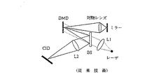
これらの欠点に関して、改良された空間的に光変調された顕微鏡がM. Liangによる“Optics Letters”(22巻、1997年、 751〜753 頁)と、対応する米国特許第5 587 832 号明細書に記載されている。この従来技術の顕微鏡が図10で概略して示されている。2次元の空間光変調器はデジタルマイクロミラー装置(以下“DMD”と言う)により形成され、これは光源(レーザまたは白色光源)から照射光をプローブへ反射し、検出光をプローブから2次元検出器へ反射する。DMDの各マイクロミラーは照射と検出スポットを形成するかしないかを個々に制御可能である。
【0008】
【発明が解決しようとする課題】
光変調器としてDMDを使用することによって共焦点画像の直接検出を可能にする。さらに共焦点性に妥協せずに最小の共焦点パターン周期(照射スポットを形成するマイクロミラーの距離)を決定することが可能である。それにもかかわらず、米国特許第5 587 832 号明細書の顕微鏡は、物体の反射光の一部のみしかイメージ形成に使用されることができないので、照射強度が制限される。さらに、イメージ形成に使用されるこの光は“焦点が合っていない”オフセットを有し、不都合な方法で共焦点画像のSNRに影響する。したがって従来技術の顕微鏡は一般的な画像を獲得する可能性なしに共焦点イメージに特定化される。
【0009】
特に細胞またはその一部等の生物物体をイメージする分野における実時間共焦点顕微鏡またはイメージでは、感度、検出速度に関する改良と、さらに測定原理の実行により応用性を拡張することが要求されている。
【0010】
本発明の目的は、特に実効的な光による区分、高い空間的解像度および/または高い光効率で急速なデータ獲得を可能にする共焦点イメージ形成のための改良された装置および方法を提供することである。本発明の特別な目的は、生物または化学材料(例えば生きた細胞、反応生成物等)の2次元または3次元イメージ、およびしたがって分子構造および機能についての情報を迅速に与えることである。固有の感度および選択性により、分子蛍光は新しいイメージ装置および方法で実行するのに好ましい分光現象である。
【0011】
【課題を解決するための手段】
前述の目的は、それぞれ請求項1または請求項14の特徴をもつ共焦点画像装置または方法により解決される。本発明の有用な実施形態は従属請求項に記載されている。
【0012】
本発明の基本的な考えは、空間光変調器手段(以下SLMとする)を有するプログラム可能な空間的に光変調された共焦点顕微鏡(以下PAMとする)として共焦点光イメージシステムの動作であり、それによって試験体または物体から出力された光出力全体は同時または順次的に集められる2つの画像に分解される。通常、空間光変調器手段は変調器素子のアレイを具備し、その透過または反射特性は個々に制御可能である。SLM変調器素子の第1のグループ(“オン”−素子)により、物体は照射され、焦点共役画像が集められ、一方、SLM変調器素子の第2のグループ(“オフ”−素子)により、非共役画像が集められる。非共役画像は焦点が合っていない光を含んでいる。SLM変調器素子により形成される焦点スポットは物体の焦点平面に焦点を結ばれる。
【0013】
顕微鏡の画像平面に位置されるとき、物体の焦点平面の異なった点に対してそれぞれ共役されたSLM素子は照射および/または検出に使用されるプログラム可能なアレイを限定する。
【0014】
第1のグループの変調器素子は個々に制御可能であり、それによって照射スポットのパターンシーケンスは時間依存性の体系的にシフトしたグリッドパターン、または有限の長さの疑似ランダムシーケンスに基づくパターンにより表される。第1のケースでは、第1の画像は共焦点画像に対応する画像であり、第2の画像は非共焦点画像と第1の画像との差画像である。第2のケースでは、第1の画像は共焦点画像と非共焦点画像の重畳であり、第2の画像は非共焦点画像と共焦点画像との差画像である。どんなケースでも、第1の画像は図2で示されているように共役画像の一部を含むことができる。
【0015】
SLMは透過または反射モードで動作されることができる。検出手段の検出器システム数に応じて、PAMはいわゆる単一通路または二重通路のPAMとして構築されることができる。好ましい配列にしたがって、共焦点光イメージシステムの光源手段は白色光ランプと、波長選択手段とを含んでいる。
【0016】
共焦点光イメージシステムの好ましい応用は、細胞および組織の生物学的調査、解析/生物工学処理、遺伝解析におけるもとの位置の交配、位置選択光化学反応のための光マスクの形成、チップ上における生化学アレイの生成および読出し、半導体産業および/または光記録および読出しにおける大規模の表面検査である。
【0017】
本発明は以下の利点を有する。PAMは現存の顕微鏡のモジュール拡張として構成されることができる。一般的なCLSMで通常拒否される焦点が合っていない光が集められ、焦点の合った画像を強調するために使用される。変調器素子の第1のグループの各素子は個々に制御可能であるかプログラム可能であり、それによって照射スポットのパターンシーケンスは、物体に関する少なくとも1つの予め定められた問題領域を照射する。(任意選択的にレーザにより)全(フル)フィールドおよび/または共焦点イメージができる高度のフレキシブルな白色光顕微鏡の構成が利用可能である。高い光スループットにより、白色光照射は顕微鏡の拡張された応用能力が得られることを可能にする。
【0018】
“オン”素子および“オフ”素子を介して伝送される両画像の同時の使用は、本発明の特有の特徴であり、特定の改良されたデコンボリューションアルゴリズムで可能である。
【0019】
【発明の実施の形態】
本発明のさらに詳細な点および利点を添付図面を参照して以下説明する。
本発明にしたがったプログラム可能なアレイ顕微鏡(PAM)は、透過のときに動作する(例えば液晶に基づいたプログラム可能な開口マスクまたはマイクロメカニカルスイッチ)空間光変調器(以下SLMとする)、または反射のときに動作する空間光変調器(例えばDMD)に基づいて、構成されることができる。以下の説明では、(1例として)DMDを有する反射SLMとを限定ではない方法で参照する。本発明を類似の方法で透過SLMで実行することができる。
【0020】
図1は本発明にしたがった蛍光PAM100 の概略図を表している。PAM100 は基本的に、白色光ランプまたはレーザ源である光源110 と、SLMとして動作するDMD120 と、イメージ光学系130 と、プローブ部分140 と、検出システム150 、160 とを含んでいる。
【0021】
DMD120 は方形ミラー 121a、 121b…からなり(1つの素子だけがそれぞれ示されている)、それぞれ垂線に対して予め定められた傾斜角度±αにわたって2つの安定な固定状態に別々に傾斜されることができる。傾斜角度αの値は実際に使用されるDMDに依存する。各ミラー素子はDMDに依存する予め定められた面積を有する。好ましいパラメータは例えば20μm以下の方形ミラーでα=±10°である。各ミラー素子は予め定められた変調パターンにしたがって、KHz範囲の特徴周波数により固定状態間で切換えられることができる。固定状態は、検出システム150 、160 へ偏向される検出された光のそれぞれの共役貢献と非共役貢献にしたがって“オン”と“オフ”位置と呼ばれる。以下概略するように得られる所望の共焦点画像に基づいて両者の貢献は焦点共役画像Ic と非共役画像Incをそれぞれ生じる。
【0022】
検出システム150 、160 は共通通路二重反射システムである。この命名法を以下の理由で使用する。“共通通路”は照射および検出が照射開口と検出開口との間の基本的に共通の光路に従うことを意味する。“二重反射”はSLM素子が光を2つの縦続的な光路に沿って導くことができることを意味する。したがって画像IncとIc (以下参照)は同時に集められることができる。二重通路単一反射システムとして別のシステムを後述する(図4)。
【0023】
再び図1を参照すると、各通路は2次元カメラ151 、161 と検出光学系111 、112 、162 をそれぞれ含んでいる。カメラ151 は“オン位置”でミラーにより反射された光を検出し、カメラ161 は“オフ位置”で反射された光を受けるように構成されている。
【0024】
以下、図1にしたがったシステムのカメラ151 による焦点共役画像Ic の検出と、カメラ161 による焦点共役画像Incの検出を説明する。検出後、画像処理、記憶、表示等のさらに別のステップが付加される。これらのステップは走査システムからよく知られているので、詳細には説明しない。
【0025】
フレーム集積期間中、SLM(DMD120 )の変調パターンは共焦点画像(走査)を発生するためにN回変更される。SLMのi番目の変調は以下のように示される。

(焦点共役画像の検出)
焦点共役画像Ic を得るため、変調Si は以下説明するグリッドパターン方法または疑似ランダムシーケンス方法にしたがって選択されることが好ましい。グリッドパターン方法は簡単な構成であり、後処理せずに共焦点画像を生成する利点を有する。疑似ランダムシーケンス方法では幾らかの後処理が必要とされるが、所定の信号レベルに対するフレーム積分時間は基本的に短い。
(i)グリッドパターン方法
グリッドパターン方法では、SLMの素子(例えばマイクロミラーまたは液晶素子)はグリッドパターンおよびシフトされた体系にしたがってオンに切換えられる。変調パターンは次式にしたがって選択される
Sa,b (xd ,yd )=G(xd −aη,yd −bη) (2)
ここで、ηは素子のサイズであり(方形素子は100%の充填率であると仮定する)、式(1)の指数iは2次元整数指数a、bにより置換され、0≦a<nx 、0≦b<ny である。グリッドは以下の特性により限定される。
【0026】
【数1】
【0027】
距離zs にわたる変位により軸方向で走査される場合の、物体空間での座標システム(x0 ,y0 ,z0 )中の物体O(x0 ,y0 ,z0 )の焦点共役画像は次式により得られる。
【0028】
【数2】
【0029】
【数3】
Φx =xd modη Φy =yd modη (6)
式(4)にしたがった画像はΦx 、Φy 、xd 、yd の依存性により空間的に可変のPSFを有する3次元のコンボリューションとして観察されることができる。SLMは連続的に走査できず、G(xd ,yd )は(いわゆるタンデム走査顕微鏡のような既知の顕微鏡における連続動作とは対照的に)ηの整数倍にわたってシフトするだけである。η/Mが画像のサンプリング密度と比較して小さいならば、差は無視できる程度である。ηが非常に大きい場合、画像の画素化が生じる。PSFはηにわたってSLMを走査することにより空間的に不変にされることができる(いわゆるデイザリング)。
【0030】
式(4)にしたがって無限に薄い蛍光平面の応答における数字のシミュレーションが、焦点平面に関する平面位置の関数として図2に示されている。シミュレーションは例えばパラメータδx =δy ={2,3,5,10,20}、η,素子サイズη=17μm、NA=1.4、M=100、励起波長λex=633nm、放射波長λex=665nm、屈折率1.515の可変格子距離の正方形グリッドに基づいている。これらのパラメータは本発明の実際的構造にのみ適合する例である。通常の顕微鏡および理想的な共焦点顕微鏡の画像と比較して結果が標準化(正規化)される。通常の応答(以下説明する図2または図5の測定されたデータの最上部線)は有限サイズの画像における無限に大きい物体をシミュレートする結果として予測された直線から偏位している。比較的小さい格子距離においてさえも、背景が増加していることによるが区分効果は明白である。格子距離間隔が増加している場合、応答はより急峻になり、背景抑圧はより効率的である。図2で示されているようなオフセット上昇の類似の動作が、有限長の疑似ランダムシーケンスにおける傾斜間隔が変化されるときに得られる。
(ii)疑似ランダムシーケンス方法
疑似ランダムシーケンス方法では、SLMの素子も有限長の疑似ランダムシーケンスにしたがって切換えられる。SLMが所定の積分フレーム内でそのパターンを変化することができる回数が限定されているので、完全に相関されていない変調の理想的な状況を実際に実現することは困難である。それ故、完全な平面はN個の2次元パターンRi (a,b)の反復されたシーケンスで変調される。数Nと1パターンの周期は、シーケンスが1フレームの積分時間と比較して短いように選択されることができる。しかしながら別の選択も可能である。パターンシーケンスRi (a,b)は以下の特性を有する。
【0031】
【数4】
【0032】
i番目のパターンを“傾斜”するための式(3)にしたがったグリッドを基礎として、完全な変調パターンSi (xd ,yd )が形成される。G(xd −aη,yd −bη)=1の全てのSLM素子がシーケンス(1+Ri (a,b))/2を使用して同一方法で切換えられる。i番目の変調は、全ての素子が同時に切換えられるとき全てのaおよびbにわたる合計により与えられる。
【0033】
【数5】
【0034】
座標システム(x0 ,y0 ,z0 )の物体O(x0 ,y0 ,z0 )の焦点共役画像は次式により得られる。
【0035】
【数6】
【0036】
式(9)にしたがった無限の薄い蛍光平面の応答における数値シミュレーションは、一定のオフセットを除いて図2の数値シミュレーションと同一である。
【0037】
疑似シーケンス方法により共焦点画像を得るため、補償項が減算されなければならない。これはJuskaitis 等により記載された前述の技術にしたがった一般的画像であるか、好ましくは非共役画像である。後者の場合、前者に関して2倍の共焦点信号が得られる。
(非共役画像の検出)
非共役画像Incは第2のカメラ161 でイメージされることができる。代わりに、共役画像Ic と同様のカメラで非共役画像Incをイメージすることが可能である。共通の通路タイプのこのような単一カメラシステムの1例を図7のA、Bを参照して以下説明する。本発明にしたがって、全ての蛍光、またはSLM上に落ちる物体から反射された光はカメラにより収集される。それ故、検出された画像の合計は通常の画像でなければならず、それによって非共役画像Incは式(4)または(9)で得られる通常の画像と共焦点画像との差である。疑似ランダムシーケンスに対して、Ic とIncの差は所望の共焦点画像に等しい。
(デコンボリューション)
画像が前述の方法にしたがって得られたならば、さらに改良された物体の再構成または回復のためにデコンボリューションアルゴリズムが条件的に実行されることができる。これはデコンボリューションアルゴリズムの性能が入力画像の特性およびSNRにより強く限定されるので基本的な利点である。共焦点顕微鏡の検出された信号が劣化した回復結果により非常に騒音が大きく、(劣化した分解能を有し区分能力がない)一般的な顕微鏡の検出された信号が非常に強く、改良されたデコンボリューションを可能にする。本発明はデコンボリューションにより共焦点イメージおよび一般的なイメージとの両者の利点を組合わせることを可能にする。前述の限定はデコンボリューションアルゴリズムにしたがって減少され、1以上の光セクションの両画像は適切な増強アルゴリズムで結合される。
【0038】
増強アルゴリズムは、3以上のセクションが単一の増強された画像を発生するために使用される最隣接方法、または画像の3Dスタックが全(フル)3D再構成に対して使用されるアルゴリズムであり、これはP. J. Verveer とT. M. Jovin の“Journal of the Optical Society of America A ”(14巻、1997年、1696〜1706)に記載されている。後者のモデルは以下のマトリックス表記で説明される。
【0039】
多次元のディスクリートな画像は画素の積重ねによりベクトルで表示される。多次元線形ぼけ(blurring)動作は1つのマトリックスにより表される。これは次のようなイメージ式を導く。
i=N[Hf+b] (10)
ここでi、f、bは検出された画像、物体、既知の背景をそれぞれ表している。顕微鏡光学系により誘発されたぼけは線形であると仮定され、マトリックスHによる乗算で与えられる。関数N[.]はベクトルアーギュメントの各素子、通常は蛍光イメージにおけるポアッソン分布へ雑音プロセスを適用することを表している。
【0040】
共役画像ic =N[Hc f+bc ]および非共役画像inc=N[Hncf+bnc]の対応する式は、ic とincを1つのベクトルにスタックし、Hc とHncを複素演算子へスタックすることによって、本発明にしたがって次のような1つの式に結合されることができる。
【0041】
【数7】
【0042】
式(10)、(11)では、画像の次元は無関係である。Hの構成は次元に依存するが、アルゴリズム自体はそれに依存しない。通常、次元は3(空間的次元)に等しい。しかしながら、スペクトルまたは時次元等のさらに別の次元が、ただ1つだけのHの変化に付加されることができる。例えば、時間依存が各画像画素または画像画素のグループで測定されるならば、次元は4に等しい。ぼけが時次元中に存在するならば、これは時次元でHを拡張することによりデータからデコンボリューションされることができる。以前は空間次元に限定されていたこれらのデコンボリューションアルゴリズムをスペクトルおよび時次元にも適用する能力は本発明の基本的な利点を表している。
(さらに別のPAM配列)
図3は本発明にしたがった共通通路二重反射PAM300 の概略図を示している。図1で示されているのと同様に、PAM300 は基本的に、光源310 、SLM320 、イメージ光学系330 、プローブ部分340 、検出システム350 、360 を含んでいる。PAM300 は側面照射ポート(例えばZeiss Axioplan)を有する顕微鏡とCCDカメラ(例えば、光度測定計のCH220 カメラ、Tucson、米国、コダックKAF1400 CCD センサ付)と組合わせた光源として(例えばテキサスインストルメント社、ダラス、米国)のデジタル光処理キットが使用されることができる。プローブ部分340 は、例えばLudl Electronics Products 社、ホーソン、米国のコンピュータ化された焦点制御装置のようなz変位(焦点平面に対して垂直)のための駆動装置を含んでいる。PAM300 は変調器素子を制御するための駆動装置、制御装置、計算およびデコンボリューション回路、表示装置(図示せず)を付加的に含んでいる。照射通路はハッチで示されている。
【0043】
(前述したように)DMDであるSLM320 は濾光された白色ランプ光源310 により照射される。フィルタは問題の予め定められた波長範囲用の帯域通過フィルタである。“オン素子” 320a(1つの素子のみを図示する)からの反射は対物レンズ342 によって対物平面341 に焦点を結ばれる。対物平面341 で励起された蛍光光は同一の光路を経てSLM320 へ戻り、ここで、光は半透明ミラー311 上で反射されてIc 路に沿ってフィルタ353 とレンズ352 を経てカメラ351 へ反射される。焦点が外れた位置(例えば図3の挿入図中の平面nc)から発生した光は“オフ”素子 321b(1つの素子のみが図示されている)によりミラー364 上で反射されてInc路に沿ってフィルタ363 とレンズ362 を経てカメラ361 へ入射される。共焦点配列は対応するSLM素子がオフに切換えられたとき焦点平面から光を拒否することを可能にする。フィルタ353 と363 は蛍光測定に適合された長波長の通過フィルタであることが好ましい(λem>λ0 )。
【0044】
図1で示されているように、焦点共役画像Ic はカメラ351 により収集され、非焦点共役画像Incはカメラ361 により収集される。
【0045】
図4は本発明の別の実施形態である二重通路単一反射PAM400 の概略図を示している。“二重通路”は照射および検出が2つの異なった光路に従うことを意味する。さらに、SLMは光を2方向で誘導することができるが、単一の反射方向だけが使用される。図3の実施形態では、共焦点は同一のSLM素子により限定され、図4にしたがって共焦点は照射側のSLM素子と、検出側のCCD画素により限定される。
【0046】
PAM400 は、1つの光軸を有する一般的な顕微鏡に簡単な方法で適合され、その光軸上にプローブ部分440 と、画像光学系430 と検出システム450 が配置されている。顕微鏡は前述した構成要素と同じ基本構成要素を具備することができる。光源410 からの照射光は顕微鏡のSLM420 と側面ポートを経て光軸上でビームスプリッタ(例えば半鍍銀ミラー)へ反射される。
【0047】
検出システム450 が1つのカメラ451 しか有しないとき、Ic とInc画像の分離はカメラ画像の解析を基礎として行われる。解析再構成と組合わせた二重通路PAMは、簡単な構成能力と高い効率と光学的処理能力とを有する利点がある。
【0048】
シフトされたグリッド方法にしたがって、“オン”素子の画像画素は最大のグレー値を選択することにより記録されたセットで発見される。DMDの各SLM素子は1つのシリーズで丁度1回だけ“オン”に切換えられ、“オン”状態の画素は最大の強度を有する。Ic 画像はこれらの選択された画素から再構成され、一方、Inc画像は残りの画素の合計から生じる。
【0049】
疑似ランダムシーケンス方法では、全体の半分を占める最も輝度の高い画像はIc 画像であり、残りの半分はInc画像である。Ic 画像とInc画像は一般的な画像と共焦点画像の和と差をそれぞれ表しているので、共焦点画像は差Ic −Incにより計算されることができる。
【0050】
図5は、(544μmのスポット距離に対応する)32×32の正方形格子と、100×1.3NA(開口の数)のオイル充填対物レンズと、λ=450〜490nmであるDMDを使用してPAMの軸応答特性を示している。反射表面の軸方向zの走査は、図2のシミュレーションにしたがって強力な光区分能力を示す強度をもつ共焦点画像を生成する。
【0051】
光区分中の背景信号の抑圧の実験による確証が図6で示されている。反射表面(ミラー)は焦点平面を通ってz軸に沿って走査される。パラメータは距離δx =δy ={3,5,10,20}η,η=17μm(16μmサイズ+ミラー間のギャップ1μmに対応する)、100×1.3NAのオイル充填対物レンズと、λ=450〜490nmである正方形格子である。
【0052】
図7のA、Bは、画像収集用に単一のカメラを使用している2つの照射軸を有する共通通路二重反射PAM700 の別の例を示している。この概念は1つのカメラだけを使用して価格を節約し、画像Ic 、Incに対する光路を形成する素子の光学的整列が簡単であるという利点を有する。
【0053】
PAM700 は図3で示されているPAM300 と基本的に類似の構成要素、特に光源 710a 、 710b、SLM720 、画像光学系730 、対物レンズ743 、プローブ部分740 、検出システム750 を具備している。1つの全(フル)画像の収集は2つのステップで行われる。画像シーケンスの収集では、画像Ic 、Incは交互に集められる。
【0054】
最初に、画像Ic は、半透明ミラー711 、SLM720 、画像光学系730 を経て、光源 710aにより第1の側面から物体を照射し、逆方向の光路に沿ってSLM720 、半透明ミラー711 、フィルタ753 、レンズ752 を経てカメラ751 により焦点平面画像を検出することにより収集される。この状況は図7のAに示されている。SLM720 の制御に使用されるパターンはSLMで表示される疑似ランダムシーケンスまたはその他のシーケンスに対応して“正”表示と呼ばれる。
【0055】
次に、図7のBで示されているように、画像Incは、第2の側面(光源 710b)から物体を照射し、前述の第1のステップでオン素子を制御するために使用したシーケンスにしたがって全てのオフ素子が制御されるいわゆる“負”表示でSLM720 を制御することにより収集される。照射光が第1のステップ照射と対称的に配置された第2の軸に沿って誘導されるとき、画像Ic 、Incの位置は逆にされる。
【0056】
種々の方法にしたがって、例えば2つの照射軸に沿ってミラーにより誘導される単一の光源により、または2つの同一の光源により2面の照射が実行されることができる。
(その他の利点および方法)
一般的な共焦点レーザ走査顕微鏡(CLSM)と比較して本発明によるPAMの改良された性能は以下のような相対的なパラメータ(PAM/CLSM)、即ちα 焦点平面における相対的放射、β 相対的な検出器の量子効率、γ 1画素当りの相対的な滞留時間、δ 走査開口の相対数から得られることができる。以下の例では、画像フィールドが103 ×103 素子(総画素数:N=106 )、グリッド周期がn=10と仮定される。したがって、δはN/n2 =104 に等しい。αとβの典型的な値は、10-2(回折が制限されているレーザ光源と比較した全(フル)フィールドランプ照射)と、10(光増倍器の陰極と比較したCCDセンサ)である。1ms(PAM)と10μs(CLSM)の滞留時間では、γは100であり、速度(δ/γ)の比例的増加を表している。α・β・γによって表される相対的な信号強度はPAMでは10倍高くなる。疑似ランダムシーケンス方法は、各SLM素子の50%の活性状態のために信号レベルのさらなる増加(この例ではn2 /2)を生じる。したがって、疑似ランダムシーケンス方法は生体内の生物サンプルの顕微鏡調査に好ましい。
【0057】
PAMは獲得速度を2桁増加させる潜在性を有する。PAMのランプ光源はCLSMのレーザよりも焦点平面で非常に低い放射を生じるが、これは並列に走査されるより多数の点(より長い滞留時間を可能にする)と、検出器におけるより高い量子効率により補償される。
【0058】
本発明は、細胞および生物組織に関する生物学、実時間の医療診断処理における中間情報としての画像データの導出、(例えば遺伝解析におけるもとの位置の交配等の)分析/生物工学処理、チップ上の生化学アレイの読出し、例えば半導体産業および/または光記録および読出し等における大規模表面検査等の好ましい応用が期待される。
【0059】
本発明による顕微鏡システムは、例えばプロテイン合成のような光化学反応を開始し同時に監視することを可能にする。適切な波長で予め定められた物質を放射することにより開始が実現され、監視はこれらの物質または反応生成物を顕微鏡測定することによって行われる。特定の応用は(例えばDNAシーケンスの合成等の)位置選択性の光化学反応のための光マスクを基体上に形成することである。
【図面の簡単な説明】
【図1】本発明にしたがった蛍光PAMの概略図。
【図2】照射スポット格子距離に依存する無限平面のイメージングのシミュレーションのグラフ。
【図3】本発明にしたがった共通通路二重反射PAMの概略図。
【図4】本発明にしたがった二重通路単一反射PAMの概略図。
【図5】PAMの軸応答特性のグラフ。
【図6】区分と背景抑圧のグラフ。
【図7】本発明にしたがった単一カメラの共通通路二重反射PAMの概略図。
【図8】光区分能力を示している本発明にしたがった顕微鏡画像の図。
【図9】回転ディスク技術(従来技術)を使用している補正されていない開口を生成するための既存のシステムの概略図。
【図10】空間的に光変調された共焦点顕微鏡(従来技術)の概略図。[0001]
BACKGROUND OF THE INVENTION
The present invention relates to a confocal point microscope, in particular a programmable and spatially light-modulated or programmable array microscope, and a microscopy method using freely programmable patterns for illumination and / or detection.
[0002]
[Prior art]
A confocal microscope with a conjugate pair of illumination and detection apertures based on a point scanning system is a useful instrument for imaging a micro object so as to investigate the micro object by direct light segmentation. Discrete aperture spots are illuminated at the objective plane of the microscope, and light reflected or fluorescent light is observed through the conjugate detection aperture in the image plane. A confocal microscope based on a scanning system with a mechanically deformed aperture disk (a so-called Nico disc with a plurality of apertures) or a rotating system configured to scan an object with a laser beam (Confocal laser scanning microscope, CSLM) is commonly used.
[0003]
Both scanning systems have certain limitations. Aperture discs have limitations with respect to the illumination field, degraded contrast and high intensity loss. Since the spacing between pinholes must be large enough to maintain the confocal effect, the transparency is typically less than 3% of the disk. On the other hand, CSLM scanning mirrors produce a low duty cycle due to sequential single point data acquisition.
[0004]
The problem of intensity loss is caused by the introduction of an aperture-correction microscope, which is “Nature” by R. Juskaitis and T. Wilson (Vol. 383, 1996, pages 804-806) and by T. Wilson and R. Juskaitis. “Optics Letters” (21, 1996, 1879-1881). Such a microscope, as schematically shown in FIG. 9, uses a multipoint light source formed by a combination of a light source and a programmable aperture mask for specimen illumination. Detection of light reflected by the specimen is performed by the camera through the same aperture mask. The aperture mask is a high speed spatial light modulator formed by an array of addressable pixels or a rotating disk with a fixed modulation code.
[0005]
The mask has an uncorrected aperture and occlusion pattern, increasing the transparency of the disk to about 50%. Due to the correlation that prevents the coding sequence used by Juskaitis et al., The detected image is a superposition of the confocal image and the general image. In order to obtain the final confocal image, it is necessary to independently detect the general image that is to be removed from the superposition (eg, by a blank sector of the rotating disk).
[0006]
This additional detection of typical images is time consuming, thereby providing only a limited data acquisition rate. The applicability of aperture correction techniques is further limited by the limitations of transparency. Therefore, fluorescence measurements are possible only in exceptional cases where high fluorescence occurs. A corresponding increase in irradiation intensity results in unacceptable photodamage or bleaching reactions.
[0007]
With regard to these drawbacks, an improved spatially light-modulated microscope is described in “Optics Letters” by M. Liang (22, 1997, pp. 751-753) and the corresponding US Pat. No. 5,587 832. It is described in. This prior art microscope is shown schematically in FIG. The two-dimensional spatial light modulator is formed by a digital micromirror device (hereinafter referred to as “DMD”), which reflects the irradiation light from the light source (laser or white light source) to the probe and detects the detection light two-dimensionally from the probe. Reflects on the vessel. Each micromirror of the DMD can individually control whether or not to form an irradiation and a detection spot.
[0008]
[Problems to be solved by the invention]
Enables direct detection of confocal images by using DMD as a light modulator. Furthermore, it is possible to determine the minimum confocal pattern period (distance of the micromirror that forms the irradiation spot) without compromising the confocality. Nevertheless, the microscope of US Pat. No. 5,587 832 has limited illumination intensity since only a part of the reflected light of the object can be used for imaging. Furthermore, this light used for image formation has an “out of focus” offset, which adversely affects the SNR of the confocal image. Thus, prior art microscopes are specialized to confocal images without the possibility of acquiring generic images.
[0009]
In real-time confocal microscopes or images, particularly in the field of imaging biological objects such as cells or parts thereof, it is required to expand the applicability by improving sensitivity and detection speed and further implementing the measurement principle.
[0010]
It is an object of the present invention to provide an improved apparatus and method for confocal imaging that allows rapid data acquisition, particularly with effective light segmentation, high spatial resolution and / or high light efficiency. It is. A particular object of the present invention is to quickly provide information about 2D or 3D images of biological or chemical materials (eg living cells, reaction products, etc.) and thus molecular structure and function. Due to its inherent sensitivity and selectivity, molecular fluorescence is a preferred spectroscopic phenomenon to perform with new imaging devices and methods.
[0011]
[Means for Solving the Problems]
The above object is solved by a confocal imaging device or method having the features of
[0012]
The basic idea of the invention is the operation of a confocal optical imaging system as a programmable spatially light-modulated confocal microscope (hereinafter PAM) with spatial light modulator means (hereinafter SLM). Yes, whereby the entire light output output from the specimen or object is broken down into two images that are collected simultaneously or sequentially. Typically, the spatial light modulator means comprises an array of modulator elements whose transmission or reflection characteristics can be individually controlled. With a first group of SLM modulator elements (“on” -elements), the object is illuminated and a focus conjugate image is collected, while with a second group of SLM modulator elements (“off” -elements) Non-conjugated images are collected. Non-conjugated images contain light that is out of focus. The focal spot formed by the SLM modulator element is focused on the focal plane of the object.
[0013]
When positioned at the image plane of the microscope, SLM elements, each conjugated to a different point in the focal plane of the object, limit the programmable array used for illumination and / or detection.
[0014]
The first group of modulator elements is individually controllable so that the pattern sequence of illumination spots is represented by a pattern based on a time-dependent systematic shifted grid pattern or a finite-length pseudo-random sequence. Is done. In the first case, the first image is an image corresponding to the confocal image, and the second image is a difference image between the non-confocal image and the first image. In the second case, the first image is a superposition of a confocal image and a non-confocal image, and the second image is a difference image between the non-confocal image and the confocal image. In any case, the first image can include a portion of the conjugate image as shown in FIG.
[0015]
The SLM can be operated in transmissive or reflective mode. Depending on the number of detector systems of the detection means, the PAM can be constructed as a so-called single-pass or double-pass PAM. According to a preferred arrangement, the light source means of the confocal light image system includes a white light lamp and wavelength selection means.
[0016]
Preferred applications of confocal optical imaging systems include biological investigations of cells and tissues, analysis / bioengineering, mating of original positions in genetic analysis, formation of photomasks for position-selective photochemical reactions, on-chip Large scale surface inspection in biochemical array generation and readout, semiconductor industry and / or optical recording and readout.
[0017]
The present invention has the following advantages. PAM can be configured as a modular extension of existing microscopes. Unfocused light, usually rejected in general CLSM, is collected and used to enhance the focused image. Each element of the first group of modulator elements is individually controllable or programmable so that the pattern sequence of illumination spots illuminates at least one predetermined problem area for the object. Highly flexible white light microscope configurations are available that allow full (full) field and / or confocal images (optionally with a laser). Due to the high light throughput, white light illumination allows the extended application capabilities of the microscope to be obtained.
[0018]
The simultaneous use of both images transmitted through “on” and “off” elements is a unique feature of the present invention and is possible with certain improved deconvolution algorithms.
[0019]
DETAILED DESCRIPTION OF THE INVENTION
Further details and advantages of the present invention will be described below with reference to the accompanying drawings.
A programmable array microscope (PAM) according to the present invention operates during transmission (eg, a programmable aperture mask or micromechanical switch based on liquid crystal), a spatial light modulator (hereinafter SLM), or reflective. Can be configured based on a spatial light modulator (eg, DMD) operating at In the following description, reference will be made in a non-limiting manner to a reflective SLM with DMD (as an example). The present invention can be implemented in a transparent SLM in a similar manner.
[0020]
FIG. 1 represents a schematic diagram of a fluorescent PAM100 according to the present invention. The
[0021]
The
[0022]
The
[0023]
Referring again to FIG. 1, each passage includes a two-
[0024]
Hereinafter, the focal conjugate image I by the
[0025]
During the frame integration period, the modulation pattern of the SLM (DMD 120) is changed N times to generate a confocal image (scan). The i th modulation of the SLM is shown as follows:
(Focus conjugate image detection)
Focus conjugate image I c To obtain the modulation S i Is preferably selected according to a grid pattern method or a pseudo-random sequence method described below. The grid pattern method has a simple configuration and has the advantage of generating a confocal image without post-processing. Although some post-processing is required in the pseudo-random sequence method, the frame integration time for a given signal level is basically short.
(I) Grid pattern method
In the grid pattern method, the SLM elements (eg, micromirrors or liquid crystal elements) are switched on according to the grid pattern and the shifted scheme. The modulation pattern is selected according to the following formula
S a, b (X d , Y d ) = G (x d -Aη, y d -Bη) (2)
Where η is the size of the element (assuming that the square element has a 100% fill factor), the index i in equation (1) is replaced by the two-dimensional integer indices a and b, and 0 ≦ a <n x , 0 ≦ b <n y It is. The grid is limited by the following characteristics.
[0026]
[Expression 1]
[0027]
Distance z s Coordinate system in object space (x 0 , Y 0 , Z 0 ) Object O (x 0 , Y 0 , Z 0 ) Is obtained by the following equation.
[0028]
[Expression 2]
[0029]
[Equation 3]
Φ x = X d modη Φ y = Y d modη (6)
The image according to equation (4) is Φ x , Φ y , X d , Y d Can be observed as a three-dimensional convolution with a spatially variable PSF. The SLM cannot scan continuously and G (x d , Y d ) Only shifts over an integral multiple of η (as opposed to continuous operation in known microscopes such as so-called tandem scanning microscopes). If η / M is small compared to the image sampling density, the difference is negligible. If η is very large, pixelation of the image occurs. The PSF can be made spatially invariant by scanning the SLM over η (so-called dithering).
[0030]
A numerical simulation of the response of an infinitely thin fluorescent plane according to equation (4) is shown in FIG. 2 as a function of plane position with respect to the focal plane. The simulation is for example parameter δ x = Δ y = {2, 3, 5, 10, 20}, η, element size η = 17 μm, NA = 1.4, M = 100, excitation wavelength λ ex = 633 nm, radiation wavelength λ ex = 665 nm, based on a square grid with a variable grating distance of refractive index 1.515. These parameters are examples that only fit the practical structure of the present invention. Results are normalized (normalized) compared to normal and ideal confocal microscope images. The normal response (the top line of the measured data in FIG. 2 or FIG. 5 described below) deviates from the line predicted as a result of simulating an infinitely large object in a finite size image. Even at relatively small grid distances, the segmentation effect is evident due to the increased background. When the grid distance spacing is increased, the response is steeper and the background suppression is more efficient. A similar behavior of increasing the offset as shown in FIG. 2 is obtained when the slope spacing in a finite length pseudo-random sequence is changed.
(Ii) Pseudo random sequence method
In the pseudo-random sequence method, the SLM elements are also switched according to a finite-length pseudo-random sequence. Since the number of times the SLM can change its pattern within a given integration frame is limited, it is difficult to actually realize the ideal situation of modulation that is not fully correlated. Therefore, a complete plane has N two-dimensional patterns R i Modulated with a repeated sequence of (a, b). The number N and the period of one pattern can be selected so that the sequence is short compared to the integration time of one frame. However, other choices are possible. Pattern sequence R i (A, b) has the following characteristics.
[0031]
[Expression 4]
[0032]
Based on the grid according to equation (3) to “tilt” the i th pattern, the complete modulation pattern S i (X d , Y d ) Is formed. G (x d -Aη, y d -Bη) = 1 all SLM elements are in sequence (1 + R i (A, b)) / 2 are used to switch in the same way. The i th modulation is given by the sum over all a and b when all elements are switched simultaneously.
[0033]
[Equation 5]
[0034]
Coordinate system (x 0 , Y 0 , Z 0 ) Object O (x 0 , Y 0 , Z 0 ) Is obtained by the following equation.
[0035]
[Formula 6]
[0036]
The numerical simulation of the response of an infinitely thin fluorescent plane according to equation (9) is identical to the numerical simulation of FIG. 2 except for a certain offset.
[0037]
In order to obtain a confocal image by the pseudo-sequence method, the compensation term must be subtracted. This is a general image according to the aforementioned technique described by Juskaitis et al., Or preferably a non-conjugated image. In the latter case, twice the confocal signal is obtained with respect to the former.
(Detecting non-conjugated images)
Non-conjugated image I nc Can be imaged by the
(Deconvolution)
Once the image has been obtained according to the method described above, a deconvolution algorithm can be conditionally executed for further improved object reconstruction or recovery. This is a fundamental advantage because the performance of the deconvolution algorithm is strongly limited by the characteristics of the input image and the SNR. The result of recovery that the detected signal of the confocal microscope is degraded is very noisy, the detected signal of a general microscope (having degraded resolution and lack of segmentation capability) is very strong and improved decon Make a revolution possible. The present invention makes it possible to combine the advantages of both confocal images and general images by deconvolution. The aforementioned limitation is reduced according to the deconvolution algorithm, and both images of one or more light sections are combined with a suitable enhancement algorithm.
[0038]
An enhancement algorithm is a nearest neighbor method in which more than two sections are used to generate a single augmented image, or an algorithm in which a 3D stack of images is used for full (full) 3D reconstruction. This is described in PJ Verveer and TM Jovin's “Journal of the Optical Society of America A” (Vol. 14, 1997, 1696-1706). The latter model is described in the following matrix notation.
[0039]
Multi-dimensional discrete images are displayed as vectors by pixel stacking. A multidimensional linear blurring operation is represented by a single matrix. This leads to the following image formula:
i = N [Hf + b] (10)
Here, i, f, and b represent the detected image, object, and known background, respectively. The blur induced by the microscope optics is assumed to be linear and is given by multiplication by the matrix H. Function N [. ] Represents applying a noise process to each element of the vector argument, usually the Poisson distribution in the fluorescence image.
[0040]
Conjugate image i c = N [H c f + b c ] And non-conjugated image i nc = N [H nc f + b nc ] Corresponding formula is i c And i nc Stack into one vector and H c And H nc Can be combined into a single expression according to the present invention by stacking into a complex operator.
[0041]
[Expression 7]
[0042]
In equations (10) and (11), the dimensions of the image are irrelevant. The configuration of H depends on the dimension, but the algorithm itself does not depend on it. Usually the dimension is equal to 3 (spatial dimension). However, additional dimensions, such as spectrum or time dimension, can be added to just one H change. For example, if time dependence is measured at each image pixel or group of image pixels, the dimension is equal to 4. If blur is present in the time dimension, it can be deconvoluted from the data by extending H in the time dimension. The ability to apply these deconvolution algorithms, previously limited to the spatial dimension, to the spectral and temporal dimensions also represents a fundamental advantage of the present invention.
(Still another PAM sequence)
FIG. 3 shows a schematic diagram of a common path double reflection PAM300 according to the present invention. Similar to that shown in FIG. 1, the
[0043]
A DMD SLM 320 (as described above) is illuminated by a filtered white lamp
[0044]
As shown in FIG. 1, the focal conjugate image I c Is collected by the
[0045]
FIG. 4 shows a schematic diagram of a dual-pass
[0046]
The
[0047]
When the
[0048]
According to the shifted grid method, “on” element image pixels are found in the recorded set by selecting the maximum gray value. Each SLM element of the DMD is switched “on” just once in a series, and the “on” pixel has the highest intensity. I c The image is reconstructed from these selected pixels, while I nc The image results from the sum of the remaining pixels.
[0049]
In the pseudo-random sequence method, the brightest image that occupies half of the total is I c The other half is I nc It is an image. I c Image and I nc Since the images represent the sum and difference of the general image and the confocal image, respectively, the confocal image is the difference I c -I nc Can be calculated by:
[0050]
FIG. 5 uses a 32 × 32 square grating (corresponding to a spot distance of 544 μm), an oil-filled objective lens of 100 × 1.3 NA (number of apertures), and a DMD with λ = 450-490 nm. The axis | shaft response characteristic of PAM is shown. Scanning the reflective surface in the axial direction z produces a confocal image with an intensity that exhibits a strong light segmentation capability according to the simulation of FIG.
[0051]
Confirmation by experiment of suppression of background signal during light segmentation is shown in FIG. The reflective surface (mirror) is scanned along the z-axis through the focal plane. Parameter is distance δ x = Δ y = {3,5,10,20} η, η = 17 μm (corresponding to 16 μm size + gap between mirrors of 1 μm), 100 × 1.3 NA oil-filled objective lens, and square grating with λ = 450 to 490 nm It is.
[0052]
FIGS. 7A and 7B show another example of a common path dual reflection PAM 700 having two illumination axes using a single camera for image acquisition. This concept saves money by using only one camera, and image I c , I nc It has the advantage that the optical alignment of the elements forming the optical path with respect to is simple.
[0053]
The PAM 700 includes components basically similar to the
[0054]
First, image I c Irradiates an object from the first side by a
[0055]
Next, as shown in FIG. nc Irradiates an object from the second side (
[0056]
According to various methods, two-sided illumination can be performed, for example, with a single light source guided by a mirror along two illumination axes, or with two identical light sources.
(Other advantages and methods)
Compared with a general confocal laser scanning microscope (CLSM), the improved performance of the PAM according to the present invention is relative parameters (PAM / CLSM) as follows: relative emission in the α focal plane, β relative Can be derived from the quantum efficiency of a typical detector, the relative dwell time per γ pixel, and the relative number of δ scan apertures. In the following example, the image field is 10 Three × 10 Three Element (total number of pixels: N = 10 6 ), The grid period is assumed to be n = 10. Therefore, δ is N / n 2 = 10 Four be equivalent to. Typical values for α and β are 10 -2 (Full (full) field lamp irradiation compared to laser light source with limited diffraction) and 10 (CCD sensor compared to photomultiplier cathode). For dwell times of 1 ms (PAM) and 10 μs (CLSM), γ is 100, representing a proportional increase in speed (δ / γ). The relative signal strength represented by α · β · γ is ten times higher in PAM. The pseudo-random sequencing method is a further increase in signal level (n in this example n) due to the 50% active state of each SLM element. 2 / 2). Therefore, the pseudo-random sequence method is preferable for microscopic examination of biological samples in vivo.
[0057]
PAM has the potential to increase acquisition speed by two orders of magnitude. The PAM lamp source produces much lower radiation in the focal plane than the CLSM laser, which has a higher number of points scanned in parallel (allowing a longer dwell time) and higher quantum at the detector. Compensated by efficiency.
[0058]
The present invention relates to biology related to cells and biological tissues, derivation of image data as intermediate information in real-time medical diagnostic processing, analysis / biotechnology processing (eg, mating of original positions in genetic analysis), on-chip Preferred applications such as large-scale surface inspection in the biochemical array readout, such as the semiconductor industry and / or optical recording and readout are expected.
[0059]
The microscope system according to the invention makes it possible to initiate and simultaneously monitor photochemical reactions such as protein synthesis. Initiation is achieved by emitting predetermined substances at appropriate wavelengths, and monitoring is performed by microscopic measurement of these substances or reaction products. A particular application is to form a photomask on a substrate for regioselective photochemical reactions (eg synthesis of DNA sequences).
[Brief description of the drawings]
FIG. 1 is a schematic diagram of a fluorescent PAM according to the present invention.
FIG. 2 is a graph of an infinite plane imaging simulation depending on the irradiation spot grid distance.
FIG. 3 is a schematic diagram of a common path double reflection PAM according to the present invention.
FIG. 4 is a schematic diagram of a double-pass single reflection PAM according to the present invention.
FIG. 5 is a graph of axial response characteristics of PAM.
FIG. 6 is a graph of classification and background suppression.
FIG. 7 is a schematic diagram of a single camera common path double reflection PAM according to the present invention.
FIG. 8 is a diagram of a microscopic image according to the present invention showing light sorting capability.
FIG. 9 is a schematic diagram of an existing system for generating an uncorrected aperture using rotating disk technology (prior art).
FIG. 10 is a schematic diagram of a spatially light-modulated confocal microscope (prior art).
Claims (24)
素子の第2のグループは物体の非共役位置で光を集めるように構成され、非共役位置からの検出光は検出器手段において第2の画像Incを形成することを特徴とする共焦点光イメージシステム。Light source means, detector means having at least one two-dimensional detector camera, and spatial light modulator means having first and second groups of modulator elements, wherein the first of the modulator elements The group is configured to illuminate an object to be inspected according to a predetermined pattern sequence of illumination spots focused to conjugate the position of the object, and the detection light from the conjugate position is detected by a detector In a confocal optical imaging system for forming a first image I c in the means,
A second group of elements is arranged to collect light at a non-conjugated position of the object, and the detected light from the non-conjugated position forms a second image I nc at the detector means. Image system.
有限長の疑似ランダムシーケンスにしたがって、またSマトリックスタイプのアダマールシーケンスにしたがって規則的な間隔またはランダムな間隔の体系的にシフトされた単数または複数のラインであり、
三角形、正方形、長方形、六角形等の規則的なドット格子と、
いわゆるウォルシュ、シルヴェスター、アダマール、またはゴレイシーケンスに基づいて有限長のランダムパターンまたは疑似ランダムパターンと、
交差するラインパターンから形成される正方形または長方形グリッドと、
全(フル)フィールド“オン”パターンと、
SLMで逐次的に生成されるとき整数の回数だけSLM素子をオン切換えするように構成された平面充填パターンと、
循環アダマールマトリックスの行または列から得られた2次元パターンの反復シーケンスと、または
上記パターンシーケンスの組合わせとから選択される請求項2または3記載の共焦点光イメージシステム。The pattern sequence is
Systematically shifted line or lines with regular or random spacing according to a finite-length pseudo-random sequence and according to an S-matrix type Hadamard sequence,
Regular dot grids such as triangles, squares, rectangles, hexagons, etc.
A random or pseudo-random pattern of finite length based on a so-called Walsh, Sylvester, Hadamard, or Golay sequence;
A square or rectangular grid formed from intersecting line patterns;
All (full) field “on” patterns,
A planar filling pattern configured to switch on an SLM element an integer number of times when sequentially generated by the SLM;
4. A confocal optical imaging system according to claim 2 or 3, selected from a repetitive sequence of two-dimensional patterns obtained from rows or columns of a cyclic Hadamard matrix, or a combination of said pattern sequences.
物体の共役位置に焦点を結ばれた照射スポットの予め定められたパターンシーケンスにしたがって検査されるべき物体に変調器素子の第1のグループから光を導き、
共役位置から検出器手段へ検出光を導くことによって検出器手段により第1の画像Ic を収集するステップを有する共焦点光イメージ形成方法において、
物体の非共役位置から検出器手段へ前記検出光を導くことによって、変調器素子の第2のグループにより物体の非共役位置から検出光を収集し、第2の画像Incを形成することを特徴とする共焦点光イメージ方法。Directing light from the light source means to a spatial light modulator means having first and second groups of modulator elements;
Directing light from a first group of modulator elements to an object to be inspected according to a predetermined pattern sequence of illumination spots focused on the conjugate position of the object;
In a confocal light imaging method comprising the steps of collecting a first image I c by a detector means by directing detection light from a conjugate position to the detector means,
Collecting the detection light from the non-conjugated position of the object by the second group of modulator elements by directing the detection light from the non-conjugated position of the object to the detector means to form a second image I nc A featured confocal light image method.
予め定められた物質を適切な波長で放射することを含む基体上の光化学反応の位置選択開始および物質または反応生成物による蛍光測定を含む同時の監視と、
分析/生物工学処理過程と、
遺伝解析におけるもとの位置の交配と、
位相変調技術および/または偏極測定等による位置選択蛍光測定および寿命時間測定と、
チップ上での生化学アレイの生成および読出しと、
半導体産業における大規模な表面検査と、
光学的な記録および読出しと、
2以上のマルチ光子顕微鏡検査と、
立体顕微鏡検査との応用に対する請求項1乃至23のいずれか1項記載の共焦点光イメージシステムまたはイメージ形成方法の使用方法。Biological investigations of cells and tissues,
Simultaneous monitoring, including location selection initiation of photochemical reaction on the substrate including emitting a predetermined substance at the appropriate wavelength and fluorescence measurement by the substance or reaction product;
Analysis / biotechnological process,
Mating of the original position in genetic analysis,
Position selective fluorescence measurement and lifetime measurement by phase modulation technique and / or polarization measurement, etc.,
Generation and readout of biochemical arrays on the chip;
Large-scale surface inspection in the semiconductor industry,
Optical recording and reading,
Two or more multi-photon microscopy,
24. A method of using a confocal optical image system or an image forming method according to any one of claims 1 to 23 for application with stereomicroscopy.
Applications Claiming Priority (2)
| Application Number | Priority Date | Filing Date | Title |
|---|---|---|---|
| EP97118354A EP0911667B1 (en) | 1997-10-22 | 1997-10-22 | Programmable spatially light modulated microscope and microscopy method |
| DE97118354.6 | 1997-10-22 |
Publications (2)
| Publication Number | Publication Date |
|---|---|
| JPH11194275A JPH11194275A (en) | 1999-07-21 |
| JP4064550B2 true JP4064550B2 (en) | 2008-03-19 |
Family
ID=8227511
Family Applications (1)
| Application Number | Title | Priority Date | Filing Date |
|---|---|---|---|
| JP30100398A Expired - Lifetime JP4064550B2 (en) | 1997-10-22 | 1998-10-22 | Programmable and spatially light-modulated microscope and microscope method |
Country Status (5)
| Country | Link |
|---|---|
| US (1) | US6399935B1 (en) |
| EP (1) | EP0911667B1 (en) |
| JP (1) | JP4064550B2 (en) |
| AT (1) | ATE236412T1 (en) |
| DE (1) | DE69720458T2 (en) |
Cited By (2)
| Publication number | Priority date | Publication date | Assignee | Title |
|---|---|---|---|---|
| CN102928970A (en) * | 2012-10-19 | 2013-02-13 | 华中科技大学 | Method and system for rapidly three-dimensionally microimaging large sample |
| KR101907782B1 (en) | 2017-04-12 | 2018-10-12 | 한국과학기술원 | Optical micorscopy device and method of measuring the image of a specimen |
Families Citing this family (98)
| Publication number | Priority date | Publication date | Assignee | Title |
|---|---|---|---|---|
| CA2307315C (en) | 1997-10-29 | 2011-04-05 | Calum Eric Macaulay | Apparatus and methods relating to spatially light modulated microscopy |
| US6388809B1 (en) | 1997-10-29 | 2002-05-14 | Digital Optical Imaging Corporation | Methods and apparatus for improved depth resolution use of out-of-focus information in microscopy |
| GB9901365D0 (en) * | 1999-01-22 | 1999-03-10 | Isis Innovations Ltd | Confocal microscopy apparatus and method |
| JP3544892B2 (en) * | 1999-05-12 | 2004-07-21 | 株式会社東京精密 | Appearance inspection method and apparatus |
| US6700606B1 (en) * | 1999-06-09 | 2004-03-02 | Activcard Ireland Limited | Micromirror optical imager |
| DE19932487A1 (en) * | 1999-07-09 | 2001-02-08 | Epigenomics Gmbh | Photolithography illumination of biological matter uses an elastic mirror surface with controlled distortion to give structured diffracted light for illuminated and unlit zones at the target surface |
| DE19960583A1 (en) * | 1999-12-15 | 2001-07-05 | Evotec Biosystems Ag | Method and device for microscopy |
| US6663560B2 (en) * | 1999-12-17 | 2003-12-16 | Digital Optical Imaging Corporation | Methods and apparatus for imaging using a light guide bundle and a spatial light modulator |
| US6530882B1 (en) * | 2000-06-30 | 2003-03-11 | Inner Vision Imaging, L.L.C. | Endoscope having microscopic and macroscopic magnification |
| JP4610713B2 (en) * | 2000-10-13 | 2011-01-12 | オリンパス株式会社 | Endoscope device |
| JP4932076B2 (en) * | 2000-10-30 | 2012-05-16 | オリンパス株式会社 | Scanning laser microscope |
| JP4153675B2 (en) * | 2001-04-10 | 2008-09-24 | 三菱重工業株式会社 | Material life evaluation system and evaluation method |
| WO2002099397A2 (en) * | 2001-06-06 | 2002-12-12 | Digital Optical Imaging Corporation | Light modulated microarray reader and methods relating thereto |
| WO2003025656A1 (en) * | 2001-09-03 | 2003-03-27 | Kabushiki Kaisha Hayashi Soken | Digital control scanning method and apparatus |
| US6885492B2 (en) | 2001-11-08 | 2005-04-26 | Imaginative Optics, Inc. | Spatial light modulator apparatus |
| DE50307047D1 (en) * | 2002-02-04 | 2007-05-31 | Zeiss Carl Surgical Gmbh | Stereo examination systems and stereo imaging apparatus and method for operating such |
| US6996292B1 (en) * | 2002-04-18 | 2006-02-07 | Sandia Corporation | Staring 2-D hadamard transform spectral imager |
| US7193775B2 (en) * | 2002-05-30 | 2007-03-20 | Dmetrix, Inc. | EPI-illumination system for an array microscope |
| JP3691837B2 (en) * | 2002-08-16 | 2005-09-07 | 株式会社林創研 | Biochip analyzer |
| US7923260B2 (en) | 2002-08-20 | 2011-04-12 | Illumina, Inc. | Method of reading encoded particles |
| US7619819B2 (en) | 2002-08-20 | 2009-11-17 | Illumina, Inc. | Method and apparatus for drug product tracking using encoded optical identification elements |
| US7508608B2 (en) | 2004-11-17 | 2009-03-24 | Illumina, Inc. | Lithographically fabricated holographic optical identification element |
| US7164533B2 (en) | 2003-01-22 | 2007-01-16 | Cyvera Corporation | Hybrid random bead/chip based microarray |
| US7900836B2 (en) | 2002-08-20 | 2011-03-08 | Illumina, Inc. | Optical reader system for substrates having an optically readable code |
| US7872804B2 (en) | 2002-08-20 | 2011-01-18 | Illumina, Inc. | Encoded particle having a grating with variations in the refractive index |
| US7901630B2 (en) | 2002-08-20 | 2011-03-08 | Illumina, Inc. | Diffraction grating-based encoded microparticle assay stick |
| US7092160B2 (en) | 2002-09-12 | 2006-08-15 | Illumina, Inc. | Method of manufacturing of diffraction grating-based optical identification element |
| US20100255603A9 (en) | 2002-09-12 | 2010-10-07 | Putnam Martin A | Method and apparatus for aligning microbeads in order to interrogate the same |
| US7706584B2 (en) * | 2002-10-22 | 2010-04-27 | Baylor College of Medicine and William Marsh Rice University | Random access high-speed confocal microscope |
| FR2848682B1 (en) | 2002-12-13 | 2005-02-18 | Commissariat Energie Atomique | LIGHTING OPTICAL MICROSCOPE MODIFIABLE STRUCTURE |
| US7339148B2 (en) * | 2002-12-16 | 2008-03-04 | Olympus America Inc. | Confocal microscope |
| US7002164B2 (en) * | 2003-01-08 | 2006-02-21 | Intel Corporation | Source multiplexing in lithography |
| JP4031716B2 (en) * | 2003-02-06 | 2008-01-09 | 株式会社コーナン・メディカル | Ophthalmic imaging device |
| DE10327987A1 (en) * | 2003-06-21 | 2005-01-20 | MAX-PLANCK-Gesellschaft zur Förderung der Wissenschaften e.V. | Confocal optical system |
| US7881502B2 (en) * | 2003-06-30 | 2011-02-01 | Weyerhaeuser Nr Company | Method and system for three-dimensionally imaging an apical dome of a plant embryo |
| EP1972983B1 (en) * | 2003-07-04 | 2009-12-02 | Vincent Lauer | Scanning imaging device for confocal microscopy with image substraction |
| US8269174B2 (en) * | 2003-07-18 | 2012-09-18 | Chemimage Corporation | Method and apparatus for compact spectrometer for multipoint sampling of an object |
| US7433123B2 (en) | 2004-02-19 | 2008-10-07 | Illumina, Inc. | Optical identification element having non-waveguide photosensitive substrate with diffraction grating therein |
| EP1622200A1 (en) | 2004-07-26 | 2006-02-01 | CSEM Centre Suisse d'Electronique et de Microtechnique SA | Solid-state photodetector pixel and photodetecting method |
| US20060066842A1 (en) * | 2004-09-30 | 2006-03-30 | Saunders Winston A | Wafer inspection with a customized reflective optical channel component |
| JP2006133499A (en) * | 2004-11-05 | 2006-05-25 | Shimadzu Corp | Confocal scanner and confocal microscope |
| AU2005307746B2 (en) | 2004-11-16 | 2011-05-12 | Illumina, Inc. | And methods and apparatus for reading coded microbeads |
| WO2006055735A2 (en) * | 2004-11-16 | 2006-05-26 | Illumina, Inc | Scanner having spatial light modulator |
| JP2006154290A (en) * | 2004-11-29 | 2006-06-15 | Hamamatsu Univ School Of Medicine | Fluorescence microscope system |
| JP2006235420A (en) * | 2005-02-28 | 2006-09-07 | Yokogawa Electric Corp | Confocal microscope |
| JP3755888B2 (en) * | 2005-06-14 | 2006-03-15 | 株式会社林創研 | Biochip online analysis system |
| GB0514656D0 (en) | 2005-07-16 | 2005-08-24 | Cairn Res Ltd | Control of illumination in microscopy |
| EP1746410B1 (en) | 2005-07-21 | 2018-08-22 | CSEM Centre Suisse d'Electronique et de Microtechnique SA - Recherche et Développement | Apparatus and method for fluorescence lifetime imaging |
| US7593156B2 (en) * | 2005-08-26 | 2009-09-22 | Leica Microsystems (Schweiz) Ag | Microscope with micro-mirrors for optional deflection and/or beam splitting |
| DE102005040471B4 (en) * | 2005-08-26 | 2007-06-21 | Leica Microsystems (Schweiz) Ag | microscope |
| EP1762877B1 (en) * | 2005-09-13 | 2010-11-17 | Albert-Ludwigs-Universität Freiburg | Microscopy method employing a spatially modulated illumination |
| US8081378B2 (en) * | 2005-10-13 | 2011-12-20 | Nikon Corporation | Microscope |
| DE102005058185A1 (en) * | 2005-12-01 | 2007-06-14 | Friedrich-Schiller-Universität Jena | Object e.g. fundus of eye, region`s fluorescence and/or reflection spectra detecting method, involves forming difference signal from accumulated signals for spectral evaluation and presentation of fluorescence and/or reflection spectra |
| JP2007171598A (en) * | 2005-12-22 | 2007-07-05 | Olympus Corp | Confocal microscope |
| GB0606788D0 (en) * | 2006-04-03 | 2006-05-10 | Ind Co Ltd | Confocal microscopy |
| US7830575B2 (en) | 2006-04-10 | 2010-11-09 | Illumina, Inc. | Optical scanner with improved scan time |
| WO2007124437A2 (en) * | 2006-04-20 | 2007-11-01 | Washington University In St. Louis | Objective-coupled selective plane illumination microscopy |
| DE102006040636B3 (en) * | 2006-05-15 | 2007-12-20 | Leica Microsystems (Schweiz) Ag | Autofocus system and method for autofocusing |
| DE102006022592B4 (en) * | 2006-05-15 | 2008-02-07 | Leica Microsystems (Schweiz) Ag | Microscope with lighting unit |
| US7460248B2 (en) * | 2006-05-15 | 2008-12-02 | Carestream Health, Inc. | Tissue imaging system |
| DE102006025149A1 (en) * | 2006-05-30 | 2007-12-06 | Leica Microsystems (Schweiz) Ag | Optical device with increased depth of field |
| DE102006027836B4 (en) * | 2006-06-16 | 2020-02-20 | Carl Zeiss Microscopy Gmbh | Microscope with auto focus device |
| US7990524B2 (en) * | 2006-06-30 | 2011-08-02 | The University Of Chicago | Stochastic scanning apparatus using multiphoton multifocal source |
| JP4891057B2 (en) * | 2006-12-27 | 2012-03-07 | オリンパス株式会社 | Confocal laser scanning microscope |
| DE102008011993A1 (en) | 2008-02-29 | 2009-09-10 | Leica Microsystems Cms Gmbh | Synchronized imaging using optical techniques and atomic force microscopy |
| EP2304411B1 (en) * | 2008-06-17 | 2019-08-28 | Koninklijke Philips N.V. | Method and device for optically examining the interior of turbid media |
| CN101655601B (en) * | 2008-08-22 | 2012-09-26 | 麦克奥迪实业集团有限公司 | Light microscope imaging method and system based on DMD structure |
| WO2010036972A1 (en) | 2008-09-25 | 2010-04-01 | The Trustees Of Columbia University In The City Of New York | Devices, apparatus and method for providing photostimulation and imaging of structures |
| KR101495096B1 (en) * | 2008-10-31 | 2015-02-25 | 삼성전자주식회사 | Apparatus and method for narrow band x-ray filtering |
| JP5852305B2 (en) * | 2009-10-28 | 2016-02-03 | カール ツァイス マイクロスコピー ゲーエムベーハーCarl Zeiss Microscopy Gmbh | Microscopy and microscope with improved resolution |
| JP5393406B2 (en) * | 2009-11-06 | 2014-01-22 | オリンパス株式会社 | Pattern projector, scanning confocal microscope, and pattern irradiation method |
| CA2781393C (en) * | 2009-11-19 | 2017-08-08 | Modulated Imaging, Inc. | Method and apparatus for analysis of turbid media via single-element detection using structured illumination |
| DE102009047198A1 (en) * | 2009-11-26 | 2011-06-01 | Universität Rostock | Microarray-based spatial filter |
| EP2369401B1 (en) * | 2010-03-23 | 2015-09-23 | Max-Planck-Gesellschaft zur Förderung der Wissenschaften e.V. | Optical modulator device and spatio-temporally light modulated imaging system |
| US8237835B1 (en) * | 2011-05-19 | 2012-08-07 | Aeon Imaging, LLC | Confocal imaging device using spatially modulated illumination with electronic rolling shutter detection |
| DE102012009836A1 (en) * | 2012-05-16 | 2013-11-21 | Carl Zeiss Microscopy Gmbh | Light microscope and method for image acquisition with a light microscope |
| DE102012217329B4 (en) * | 2012-09-25 | 2024-03-21 | Carl Zeiss Jena Gmbh | Projection device |
| DE102013001238B4 (en) * | 2013-01-25 | 2020-06-10 | Carl Zeiss Microscopy Gmbh | Light microscope and microscopy method |
| CN103364345B (en) * | 2013-06-25 | 2015-11-11 | 浙江大学 | Based on total reflection microscope circular scan method and the device of digital micromirror elements |
| US9535242B1 (en) * | 2014-06-26 | 2017-01-03 | Verily Life Sciences Llc | Parallel programmable array microscope |
| US9485491B2 (en) * | 2014-12-15 | 2016-11-01 | Test Research, Inc. | Optical system |
| KR20160115682A (en) * | 2015-03-25 | 2016-10-06 | 삼성전자주식회사 | Method of enabling spatially varying auto focusing of objects and an image capturing system thereof |
| DE102015210016A1 (en) * | 2015-06-01 | 2016-12-01 | Carl Zeiss Microscopy Gmbh | Method for determining a spatially resolved height information of a sample with a wide field microscope and a wide field microscope |
| CN105092603B (en) * | 2015-09-07 | 2017-09-05 | 哈尔滨理工大学 | The online vision inspection apparatus and method of bowl-type workpiece inner wall |
| WO2017112634A1 (en) | 2015-12-21 | 2017-06-29 | Verily Life Sciences Llc | Spectrally and spatially multiplexed fluorescent probes for in situ cell labeling |
| WO2017162256A1 (en) | 2016-03-24 | 2017-09-28 | Max-Planck-Gesellschaft zur Förderung der Wissenschaften e. V. | Spatio-temporally light modulated imaging system including vertical cameras, and method for confocal imaging an object |
| JP6815412B2 (en) * | 2016-03-24 | 2021-01-20 | マツクス−プランク−ゲゼルシヤフト ツール フエルデルング デル ヴイツセンシヤフテン エー フアウMAX−PLANCK−GESELLSCHAFT ZUR FOeRDERUNG DER WISSENSCHAFTEN E.V. | Spatio-temporal photomodulation imaging system, confocal imaging method for objects, and carrier wheel equipment |
| US10551604B2 (en) | 2016-05-27 | 2020-02-04 | Verily Life Sciences Llc | Spatial light modulator based hyperspectral confocal microscopes and methods of use |
| DE102016119727A1 (en) * | 2016-10-17 | 2018-04-19 | Carl Zeiss Microscopy Gmbh | Device for beam manipulation for a scanning microscope and microscope |
| JP2019066706A (en) | 2017-10-02 | 2019-04-25 | ソニー株式会社 | Fluorescence microscope device and fluorescence microscope system |
| JP7053845B2 (en) * | 2017-12-20 | 2022-04-12 | マツクス-プランク-ゲゼルシヤフト ツール フエルデルング デル ヴイツセンシヤフテン エー フアウ | Methods and equipment for optical confocal imaging using a programmable array microscope |
| JP7260966B2 (en) * | 2018-02-19 | 2023-04-19 | 京セラ株式会社 | Electromagnetic wave detector |
| WO2019159933A1 (en) * | 2018-02-19 | 2019-08-22 | 京セラ株式会社 | Electromagnetic wave detection device and information acquisition system |
| EP3835845A4 (en) | 2018-08-09 | 2021-09-08 | Sony Group Corporation | Optical microscope device and optical microscope system |
| DE102018127281A1 (en) * | 2018-10-31 | 2020-04-30 | Carl Zeiss Microscopy Gmbh | Microscope and microscopy method |
| DE102019110869A1 (en) * | 2018-12-21 | 2020-06-25 | Leica Microsystems Cms Gmbh | microscope |
| CN113302520A (en) * | 2019-01-16 | 2021-08-24 | 株式会社小糸制作所 | Imaging device, arithmetic processing device therefor, vehicle lamp, vehicle, and sensing method |
| CN114930222A (en) * | 2020-01-13 | 2022-08-19 | 海克-斯特莱特股份公司 | Ophthalmic microscope with micro-mirror balancing |
Family Cites Families (6)
| Publication number | Priority date | Publication date | Assignee | Title |
|---|---|---|---|---|
| DE59107758D1 (en) * | 1990-11-10 | 1996-06-05 | Groskopf Rudolf Dr Ing | Optical scanning device with confocal beam path, in which light source and detector matrix are used |
| US5532873A (en) * | 1993-09-08 | 1996-07-02 | Dixon; Arthur E. | Scanning beam laser microscope with wide range of magnification |
| US5587832A (en) * | 1993-10-20 | 1996-12-24 | Biophysica Technologies, Inc. | Spatially light modulated confocal microscope and method |
| GB9603788D0 (en) * | 1996-02-22 | 1996-04-24 | Isis Innovation | Confocal microscope |
| DE69729659T2 (en) * | 1996-02-28 | 2005-06-23 | Johnson, Kenneth C., Santa Clara | MIKROLINSEN RASTER DEVICE FOR MICROLITHOGRAPHY AND FOR CONFOCUS MICROSCOPY WITH LARGE RECORDING FIELD |
| US6038067A (en) * | 1996-05-23 | 2000-03-14 | The Regents Of The University Of California | Scanning computed confocal imager |
-
1997
- 1997-10-22 AT AT97118354T patent/ATE236412T1/en not_active IP Right Cessation
- 1997-10-22 EP EP97118354A patent/EP0911667B1/en not_active Expired - Lifetime
- 1997-10-22 DE DE69720458T patent/DE69720458T2/en not_active Expired - Lifetime
-
1998
- 1998-10-21 US US09/176,240 patent/US6399935B1/en not_active Expired - Lifetime
- 1998-10-22 JP JP30100398A patent/JP4064550B2/en not_active Expired - Lifetime
Cited By (3)
| Publication number | Priority date | Publication date | Assignee | Title |
|---|---|---|---|---|
| CN102928970A (en) * | 2012-10-19 | 2013-02-13 | 华中科技大学 | Method and system for rapidly three-dimensionally microimaging large sample |
| CN102928970B (en) * | 2012-10-19 | 2014-10-29 | 华中科技大学 | Method and system for rapidly three-dimensionally microimaging large sample |
| KR101907782B1 (en) | 2017-04-12 | 2018-10-12 | 한국과학기술원 | Optical micorscopy device and method of measuring the image of a specimen |
Also Published As
| Publication number | Publication date |
|---|---|
| DE69720458D1 (en) | 2003-05-08 |
| EP0911667B1 (en) | 2003-04-02 |
| US6399935B1 (en) | 2002-06-04 |
| DE69720458T2 (en) | 2004-02-26 |
| EP0911667A1 (en) | 1999-04-28 |
| ATE236412T1 (en) | 2003-04-15 |
| JPH11194275A (en) | 1999-07-21 |
Similar Documents
| Publication | Publication Date | Title |
|---|---|---|
| JP4064550B2 (en) | Programmable and spatially light-modulated microscope and microscope method | |
| US10795144B2 (en) | Microscopy with structured plane illumination and point accumulation for imaging and nanoscale topography | |
| CN110262026B (en) | Aperture scanning Fourier ptychographic imaging | |
| Verveer et al. | Theory of confocal fluorescence imaging in the programmable array microscope (PAM) | |
| Neil et al. | Real time 3D fluorescence microscopy by two beam interference illumination | |
| JP5087178B2 (en) | Apparatus and method for inspection and manipulation of microscope objects | |
| JP7233129B2 (en) | Apparatus and method for fast volumetric fluorescence microscopy utilizing temporally multiplexed lightsheets | |
| US8504140B2 (en) | Apparatus and method for fluorescence imaging and tomography using spatially structured illumination | |
| US20110267688A1 (en) | Microscopy Method and Microscope With Enhanced Resolution | |
| JPH11249023A (en) | Confocal spectral system and spectral method | |
| US20220205919A1 (en) | Widefield, high-speed optical sectioning | |
| JP2004170977A (en) | Method and arrangement for optically grasping sample with depth of resolution | |
| JP2012515930A (en) | System, method and computer-accessible medium for providing a wide-field super-resolution microscope | |
| EP2831657B1 (en) | Improved confocal microscopy methods and devices | |
| Boyer et al. | Biomedical three–dimensional holographic microimaging at visible, ultraviolet and X–ray wavelengths | |
| NL2008873C2 (en) | Method and apparatus for multiple points of view three-dimensional microscopy. | |
| US20130250088A1 (en) | Multi-color confocal microscope and imaging methods | |
| JP4615941B2 (en) | Optical signal analysis method | |
| KR20220074886A (en) | High-speed scanning system for ultra-high-resolution imaging | |
| JP7268144B2 (en) | Method and apparatus for scanning a sample | |
| Enderlein | Advanced fluorescence microscopy | |
| US11156818B2 (en) | Flexible light sheet generation by field synthesis | |
| EP3627205A1 (en) | Confocal laser scanning microscope configured for generating line foci | |
| CN111189807A (en) | Fluorescence microscopy based on fluctuations | |
| WO2024044981A1 (en) | Super-resolution analysis system and method, and corresponding imaging device and model training method |
Legal Events
| Date | Code | Title | Description |
|---|---|---|---|
| A621 | Written request for application examination |
Free format text: JAPANESE INTERMEDIATE CODE: A621 Effective date: 20051014 |
|
| A977 | Report on retrieval |
Free format text: JAPANESE INTERMEDIATE CODE: A971007 Effective date: 20071128 |
|
| TRDD | Decision of grant or rejection written | ||
| A01 | Written decision to grant a patent or to grant a registration (utility model) |
Free format text: JAPANESE INTERMEDIATE CODE: A01 Effective date: 20071204 |
|
| A61 | First payment of annual fees (during grant procedure) |
Free format text: JAPANESE INTERMEDIATE CODE: A61 Effective date: 20071227 |
|
| R150 | Certificate of patent or registration of utility model |
Free format text: JAPANESE INTERMEDIATE CODE: R150 |
|
| FPAY | Renewal fee payment (event date is renewal date of database) |
Free format text: PAYMENT UNTIL: 20110111 Year of fee payment: 3 |
|
| FPAY | Renewal fee payment (event date is renewal date of database) |
Free format text: PAYMENT UNTIL: 20110111 Year of fee payment: 3 |
|
| FPAY | Renewal fee payment (event date is renewal date of database) |
Free format text: PAYMENT UNTIL: 20120111 Year of fee payment: 4 |
|
| FPAY | Renewal fee payment (event date is renewal date of database) |
Free format text: PAYMENT UNTIL: 20130111 Year of fee payment: 5 |
|
| R250 | Receipt of annual fees |
Free format text: JAPANESE INTERMEDIATE CODE: R250 |
|
| R250 | Receipt of annual fees |
Free format text: JAPANESE INTERMEDIATE CODE: R250 |
|
| R250 | Receipt of annual fees |
Free format text: JAPANESE INTERMEDIATE CODE: R250 |
|
| R250 | Receipt of annual fees |
Free format text: JAPANESE INTERMEDIATE CODE: R250 |
|
| R250 | Receipt of annual fees |
Free format text: JAPANESE INTERMEDIATE CODE: R250 |
|
| EXPY | Cancellation because of completion of term |