JP4063255B2 - Vibrating piece manufacturing method, vibrator manufacturing method, oscillator manufacturing method, and electronic device manufacturing method - Google Patents
Vibrating piece manufacturing method, vibrator manufacturing method, oscillator manufacturing method, and electronic device manufacturing method Download PDFInfo
- Publication number
- JP4063255B2 JP4063255B2 JP2004182630A JP2004182630A JP4063255B2 JP 4063255 B2 JP4063255 B2 JP 4063255B2 JP 2004182630 A JP2004182630 A JP 2004182630A JP 2004182630 A JP2004182630 A JP 2004182630A JP 4063255 B2 JP4063255 B2 JP 4063255B2
- Authority
- JP
- Japan
- Prior art keywords
- groove
- manufacturing
- resist pattern
- electrode
- vibrating piece
- Prior art date
- Legal status (The legal status is an assumption and is not a legal conclusion. Google has not performed a legal analysis and makes no representation as to the accuracy of the status listed.)
- Expired - Fee Related
Links
Images


Description
本発明は、例えば水晶等からなる振動片の製造方法、この振動片を有する振動子の製造方法、この振動子を備える発振器の製造方法や電子機器の製造方法に関する。 The present invention is, for example, a method of manufacturing a resonator element composed of quartz or the like, a method of manufacturing a transducer having the vibrating element, a method of manufacturing a manufacturing method and an electronic apparatus of an oscillator provided with the vibrator.
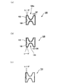
従来、振動片である音叉型水晶振動片は、例えば図12に示すように構成されている。
すなわち、音叉型水晶振動片10は、基部11と、この基部11から突出して形成されている2本の腕部12,13を有している。そして、この2本脳で部12,13には、溝12a,13aが表面に形成されている。また、この溝は図12の腕部12,13の裏面側にも同様に形成されている。
このため、図12のA−A’断面図である図13に示すように腕部12,13は、その断面形状が略H型の形成されている。
Conventionally, a tuning fork type crystal vibrating piece, which is a vibrating piece, is configured as shown in FIG. 12, for example.
That is, the tuning fork type
For this reason, as shown in FIG. 13 which is an AA ′ sectional view of FIG. 12, the
このような略H型の音叉型水晶振動片10は、振動片の大きさを小型化しても、腕部12,13の振動損失が低くCI値(クリスタルインピーダンス又は等価直列抵抗)も低く抑えることができるという特性を有する。
このため、略H型の音叉型水晶振動片10は、例えば特に小型でも高精度な性能が求められる振動子に適用されている。
略H型の音叉型水晶振動片10の大きさとしては、例えば図12に示すように腕部12,13の長さが1.644mm、幅が0.1mmとなっており、この腕部12,13に幅0.07mmの幅で溝12a,13aが形成されている。
さらに、基部11は図において縦方向の長さが0.7mmとなっている。
Such a substantially H-shaped tuning-fork type
For this reason, the substantially H-shaped tuning-fork type
The size of the substantially H-shaped tuning-fork type
Further, the
このように極めて小型の音叉型水晶振動片10であっても、近年の電気機器等の装置の小型化の要請に対応するには、更なる小型化が求められている。
この小型化の要請に対応するには、基部11の図12における縦方向の長さを0.7mmより短く形成すれば、全体として振動片10の長さが短くなり、振動片10が小型化され、最も良いのであるが、以下のような問題があった。
すなわち、一般に基部11の長さを腕部12,13の長さの40%以上としないと、振動片の固定バラツキによる影響が出やすく振動片素子間のCI値バラツキの発生が生じ易いという問題があった。
具体的には、腕部12,13の幅をW、腕部12,13の長さをLとした場合、音叉型水晶振動片10の周波数fは、
f∝W/L2 ・・・・・・・式1
の関係式を満たさなければならない。すなわち、振動片10の腕部12,13の長さLを短くすればするほど、腕部12,13の幅Wも細くなるという関係になっている。
Thus, even the extremely small tuning-fork type
In order to meet this demand for miniaturization, if the length of the
That is, generally, unless the length of the
Specifically, if the width of the
f∝W / L2 ・ ・ ・ ・ ・ ・ ・ ・ ・ ・ ・ Formula 1
The following relational expression must be satisfied. That is, the shorter the length L of the
図12に示す音叉型水晶振動片10は、上述のように小型化されているため腕部12,13の長さLが1.644mmと短いため、その幅も0.1mmと極めて細くなっている。さらに腕部12,13の厚みも0.1mmと成っている。
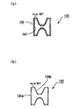
ところで、音叉型水晶振動片10の腕部12,13は、図13(a)に示すように、幅Wが長く厚みDが短ければ、図において矢印Bに示すように通常の水平方向の振動を行うことになる。
しかし、上述にように幅Wが短くなると、図13(b)に示すように、垂直方向の成分(図において矢印Cの方向)を含むようになり、図13(b)において矢印Eで示す方向に腕部12,13が振動するようになる。
これは、垂直振動成分変位量(nm)は、腕部12,13の幅W/厚みDが1.2より小さくなると急激に変位量も大きくなることによる。
Since the tuning-fork type
Meanwhile, the
However, when the width W is shortened as the above, as shown in FIG. 1 3 (b), now includes a vertical direction component (the direction of arrow C in the figure), an arrow E in FIG. 1 3 (b) The
This vertical vibration component displacement (nm), the width W / thickness D of the
このように腕部12,13の振動の垂直成分が増加し、腕部12,13が動くと、この振動が振動片10の基部11へと伝わり、振動片10をパッケージ等に固定する基部11の固定領域の接着剤等からエネルギーが逃げてしまうことになる。
このように振動が基部11へ漏れ、基部11の固定領域からエネルギーが逃げると、振動片の固定バラツキの影響によって、腕部12,13の振動が振動片によっては不安定となるものが生じ、CI値の素子間のバラツキが大きくなっていた。
そして、このような腕部12,13の振動の漏れや基部11の固定領域からのエネルギーの逃げを防ぐには、上述のように腕部12,13の長さLの40%以上の長さを基部11において確保しなければならなかった。したがって、これが振動片10自体の小型化の障害となっていた。
Thus, when the vertical component of the vibration of the
When the vibration leaks to the
In order to prevent such leakage of vibration of the
本発明は上記問題に鑑み、基部を短くしてもCI値の振動片素子間のバラツキが安定すると共に振動片全体も小型化できる振動片の製造方法、これを有する振動子の製造方法、この振動子を備える発振器の製造方法及び電子機器の製造方法を提供することを目的とする。 In view of the above-described problems, the present invention provides a method for manufacturing a resonator element that can stabilize the variation between CI resonator elements even when the base portion is shortened, and can reduce the size of the entire resonator element, and a method for manufacturing a resonator having the same. It is an object of the present invention to provide a method for manufacturing an oscillator including a vibrator and a method for manufacturing an electronic device.
前記目的は、切り込み部を有する基部と、前記基部から突出して形成され、その表面部及び/又は裏面部に溝部が形成されている振動腕部を有し、前記溝部内に溝電極が形成され、前記振動腕部の側面に側面電極が形成されている振動片の製造方法であって、前記振動片に電極膜を形成する電極膜形成工程と、前記溝電極と前記側面電極とをパターニングするためのレジストパターンを形成するレジストパターン形成工程と、前記レジストパターン形成工程で前記レジストパターンにより形成された短絡防止用間隔を調整するために、前記レジストパターンの外形に対してレーザを照射するパターン形状調整工程と、前記レジストパターンをマスクとして前記電極膜をエッチングし、前記溝電極と前記側面電極を形成する工程と、を有することを特徴とする振動片の製造方法により、達成される。 The object is to have a base portion having a cut portion and a vibrating arm portion that protrudes from the base portion and has a groove portion formed on a front surface portion and / or a back surface portion thereof, and a groove electrode is formed in the groove portion. A method of manufacturing a vibrating piece in which a side electrode is formed on a side surface of the vibrating arm, the electrode film forming step of forming an electrode film on the vibrating piece, and patterning the groove electrode and the side electrode A resist pattern forming step for forming a resist pattern, and a pattern shape for irradiating a laser to the outer shape of the resist pattern in order to adjust a short-circuit prevention interval formed by the resist pattern in the resist pattern forming step An adjustment step, and a step of etching the electrode film using the resist pattern as a mask to form the groove electrode and the side electrode. The manufacturing method of the vibrator element, characterized in, it is achieved.
前記構成によれば、前記基部に切り込み部が形成されているので、振動腕部が振動する際に、垂直方向成分を有した振動が生じても、振動腕部の振動が基部側へ漏れるのを、この切り込み部で緩和することができる。したがって、基部を小型化しながら、CI値の振動片素子間のバラツキを安定化させることができる。
また、振動片の製造方法に用いる例えば、フォトレジストは、電極膜150上に塗布さえれるが、図17(a)の音叉腕120の角部であるエッジ部分(図における矢印E)をカバーするように塗布する必要がある。このとき、塗布するフォトレジストが粒子状になっていた方がエッジ部分Eのカバーが良い。
しかしながら、フォトレジストをこのように粒子状のものを含んだ状態で塗布すると、フォトレジスト現像後のフォトレジストパターン152の外形は正確な略直線ではなく、粒子の外形に沿った略波線に形成されてしまう。
このようにフォトレジストパターン152の外形線が、不均一であると前記短絡防止用間隔が例えば、15μmという微細な間隔を形成する場合、部分的に間隔が保持されないおそれがある。
間隔が保持されない場合は、エッチングされない部分となってしまうため、溝電極と側面電極同士が短絡するおそれがある。
そのため、本発明では、前記レジストパターン形成工程で前記レジストパターンにより形成された短絡防止用間隔を調整するために、前記レジストパターンの外形に対してレーザを照射するパターン形状調整工程を有している。
すなわち、レーザをレジストパターンの一部の形状である短絡防止用間隔について照射される。
つまり、レジストパターンの外形線が不均一となり、レジストパターンをマスクとしてエッチングした場合、形成される溝電極と側面電極とが短絡等を生じないように、短絡防止用間隔が確保できるように、レジストパターンの外形がレーザによって調整される。
したがって、レジストパターンがレーザによって正確に形成された後、前記レジストパターンをマスクとして前記電極膜をエッチングし、前記溝電極と前記側面電極を形成する工程を行えば、短絡防止用間隔を正確に確保することができる。
以上のようにして製造された振動片は、振動腕部の例えば、腕表面及び腕裏面の短絡防止用間隔W1が例えば15μmに正確保持され、溝電極と側面電極とが短絡等することを有効に防止することができ、不良が生じにくい振動片となる。
また、レジストパターンを形成してからレーザを照射するので、特に例えばフォトレジストの感光を防止するイエロールーム内でレーザを照射する必要がないので製造コストを低減することができる。 According to the above configuration, since the cut portion is formed in the base portion, when the vibrating arm portion vibrates, even if vibration having a vertical component occurs, the vibration of the vibrating arm portion leaks to the base side. Can be relaxed by this cut portion. Therefore, it is possible to stabilize the variation between the resonator element having the CI value while reducing the size of the base.
Further, for example, the photoresist used in the method for manufacturing the resonator element can be applied on the
However, when the photoresist is applied in such a state including particulate matter, the outer shape of the
As described above, when the outline of the
When the interval is not maintained, the groove electrode and the side electrode may be short-circuited because the portion is not etched.
Therefore, in this invention, in order to adjust the space | interval for short circuit prevention formed with the said resist pattern at the said resist pattern formation process, it has the pattern shape adjustment process of irradiating a laser with respect to the external shape of the said resist pattern. .
That is, the laser is irradiated for the short-circuit prevention interval which is a part of the resist pattern.
In other words, when the resist pattern has a non-uniform outline and is etched using the resist pattern as a mask, the resist pattern is provided so that a short-circuit prevention interval can be secured so as not to cause a short circuit between the groove electrode and the side electrode formed. The outer shape of the pattern is adjusted by the laser.
Therefore, after the resist pattern is accurately formed by the laser, the electrode film is etched using the resist pattern as a mask, and the groove electrode and the side electrode are formed. can do.
The vibrating piece manufactured as described above is effective in that the shorting prevention interval W1 between the vibrating arm portion, for example, the arm surface and the arm back surface is accurately maintained at, for example, 15 μm, and the groove electrode and the side electrode are short-circuited. Therefore, the vibration piece is less likely to be defective.
Further, since the laser is irradiated after forming the resist pattern, it is not necessary to irradiate the laser particularly in a yellow room for preventing the photoresist from being exposed to light, so that the manufacturing cost can be reduced.
好ましくは、前記レーザがYAGレーザの3倍高調波を用いている。 Preferably, the laser uses a third harmonic of a YAG laser.
前記構成によれば、YAGレーザを用いているので、レジストパターンの外形をより正確に調整することができる。According to the said structure, since the YAG laser is used, the external shape of a resist pattern can be adjusted more correctly.
好ましくは、記溝部が前記振動腕部の表面部及び裏面部に形成され、前記レジストパターン形成工程で、前記表面部及び前記裏面部に形成された前記レジストパターンで成る前記表面部及び前記裏面部の前記短絡防止用間隔を調整するために、同時に前記レーザを照射する。 Preferably, the groove portion is formed on the front surface portion and the back surface portion of the vibrating arm portion, and the front surface portion and the back surface portion formed of the resist pattern formed on the front surface portion and the back surface portion in the resist pattern forming step. In order to adjust the short-circuit prevention interval, the laser is irradiated simultaneously.
前記構成によれば、レジストパターンで成る表面部及び裏面部の短絡防止用間隔を調整するために、同時にレーザを照射するので、表面部と裏面部の両方の調整を同時にできる。このため、振動片の生産工程を減らすことができるので生産コストを下げることできる。 According to the said structure, in order to adjust the space | interval for short circuit prevention of the surface part and back surface part which consist of a resist pattern, since a laser is irradiated simultaneously, both the front surface part and a back surface part can be adjusted simultaneously. For this reason, since the production process of the resonator element can be reduced, the production cost can be reduced.
好ましくは、前記振動腕部が略直方体でなり、その表面部の短辺である腕部幅が50μm以上150μm以下である。Preferably, the vibrating arm portion is a substantially rectangular parallelepiped, and an arm portion width which is a short side of the surface portion is not less than 50 μm and not more than 150 μm.
前記振動腕部が略直方体でなり、その表面部の短辺である腕部幅が50μm以上150μm以下である。このような振動片においても、前記切り込み部を設けることで、基部を小型化でき、振動片全体を超小型化できると共に、実用的なCI値の上限である100KΩ以下で、CI値の振動片素子間のバラツキを安定化させることができる。The vibrating arm portion is a substantially rectangular parallelepiped, and an arm width which is a short side of the surface portion is 50 μm or more and 150 μm or less. Also in such a resonator element, by providing the cut portion, the base can be reduced in size, the entire resonator element can be reduced in size, and the resonator element having a CI value of 100 KΩ or less, which is an upper limit of a practical CI value. Variations between elements can be stabilized.
好ましくは、前記振動腕部の表面部及び裏面部に溝部が形成されていると共に、前記表面部又は前記裏面部に設けられている溝部のいずれかの深さが、前記振動腕部の深さ方向の全長である厚みに対して30%以上50%未満の深さに形成されている。 Preferably, a groove portion is formed on the front surface portion and the back surface portion of the vibrating arm portion, and the depth of either the groove portion provided on the front surface portion or the back surface portion is the depth of the vibrating arm portion. It is formed to a depth of 30% or more and less than 50% with respect to the thickness which is the total length in the direction .
前記表面部又は前記裏面部に設けられている溝部のいずれかの深さが、前記振動腕部の深さ方向の全長である厚みに対して30%以上50%未満の深さに形成されているので、超小型振動片でもCI値を実用上の上限である100KΩ以下に抑えることができる。また、前記切り込み部を設けることで、CI値の振動片素子間のバラツキを安定化させることができる。The depth of any of the groove portions provided in the front surface portion or the back surface portion is formed to a depth of 30% or more and less than 50% with respect to the thickness that is the total length in the depth direction of the vibrating arm portion. Therefore, the CI value can be suppressed to a practical upper limit of 100 KΩ or less even with a micro vibrating piece. In addition, by providing the cut portion, it is possible to stabilize the variation between the resonator elements having the CI value.
好ましくは、前記表面部又は前記裏面部に設けられている溝部のいずれかの深さが、前記振動腕部の深さ方向の全長である厚みに対して40%以上50%未満の深さに形成されている。 Preferably, the depth of any of the groove portions provided in the front surface portion or the back surface portion is a depth of 40% or more and less than 50% with respect to a thickness that is a total length in the depth direction of the vibrating arm portion. Is formed.
前記表面部又は前記裏面部に設けられている溝部のいずれかの深さが、前記振動腕部の深さ方向の全長である厚みに対して40%以上50%未満の深さに形成されているので、超小型振動片でもCI値を実用上の上限である100KΩ以下により精度良く抑えることができる。The depth of any one of the groove portions provided in the front surface portion or the back surface portion is formed to a depth of 40% or more and less than 50% with respect to the thickness that is the total length in the depth direction of the vibrating arm portion. Therefore, the CI value can be accurately suppressed even with a micro vibrating piece by a practical upper limit of 100 KΩ or less.
好ましくは、前記溝部の開口における短辺である溝幅が、前記振動腕部の前記腕部幅の40%以上と成っている。 Preferably, a groove width which is a short side in the opening of the groove portion is 40% or more of the arm portion width of the vibrating arm portion .
前記溝部の開口における短辺である溝幅が、前記振動腕部の前記腕部幅の40%以上と成っているので、CI値を実用上の上限である100KΩ以下に抑えることができる。また、前記切り込み部を設けることで、CI値の振動片素子間のバラツキを安定化させることができる。Since the groove width which is the short side in the opening of the groove portion is 40% or more of the arm width of the vibrating arm portion, the CI value can be suppressed to 100 KΩ or less which is a practical upper limit. In addition, by providing the cut portion, it is possible to stabilize the variation between the resonator elements having the CI value.
好ましくは、前記溝幅が前記腕部幅の70%以上100%未満に形成されている。 Preferably, the groove width is 70% or more and less than 100% of the arm width .
前記溝幅が前記腕部幅の70%以上100%未満に形成されているので、前記切り込み部を設けることで、CI値の振動片素子間のバラツキをより安定化させることができる。Since the groove width is formed to be 70% or more and less than 100% of the arm portion width, by providing the cut portion, it is possible to further stabilize the variation between the resonator element having the CI value.
好ましくは、前記基部には、この振動片を固定させるための固定領域が設けられていると共に、前記切り込み部は、この固定領域と前記振動腕部との間の基部に設けられている。 Preferably, the base portion is provided with a fixing region for fixing the vibrating piece, and the cut portion is provided at a base portion between the fixing region and the vibrating arm portion .
前記切り込み部は、この固定領域と前記振動腕部との間の基部に設けられている。したがって、この切り込み部は、前記振動腕部の振動の妨げにならない位置に配置されていると共に、振動漏れが前記固定領域へ伝わり、エネルギーの逃げが生じるのを有効に防止している。このため、CI値の振動片素子間のバラツキが安定化する。The cut portion is provided at a base portion between the fixed region and the vibrating arm portion. Therefore, the cut portion is disposed at a position that does not hinder the vibration of the vibrating arm portion, and effectively prevents vibration leakage from being transmitted to the fixed region and energy escape. For this reason, the variation between the resonator elements of the CI value is stabilized.
好ましくは、前記振動片が略30KHz乃至略40KHzで発振する水晶で形成されている音叉振動片である。 Preferably, the vibrating piece is a tuning fork vibrating piece formed of quartz crystal that oscillates at about 30 KHz to about 40 KHz .
前記振動片が略30KHz乃至略40KHzで発振する水晶で形成されている音叉型振動片に前記切り込み部を設けることで、基部を小型化でき、音叉型振動片全体も小型化でき、CI値の振動片素子間のバラツキも安定化させることができる。By providing the notch portion in the tuning fork type vibrating piece formed of quartz crystal that oscillates at about 30 KHz to about 40 KHz, the base can be downsized, the entire tuning fork type vibrating piece can be downsized, and the CI value can be reduced. Variations between the resonator element elements can also be stabilized.
前記目的は、切り込み部を有する基部と、前記基部から突出して形成され、その表面部及び/又は裏面部に溝部が形成されている振動腕部を有し、前記溝部内に溝電極が形成され、前記振動腕部の側面に側面電極が形成されている振動片がパッケージ内に収容されている振動子の製造方法であって、前記振動片に電極膜を形成する電極膜形成工程と、The object is to have a base portion having a notch portion and a vibrating arm portion that protrudes from the base portion and has a groove portion formed on a front surface portion and / or a back surface portion thereof, and a groove electrode is formed in the groove portion. A vibrator manufacturing method in which a vibrating piece having a side electrode formed on a side surface of the vibrating arm portion is housed in a package, and an electrode film forming step of forming an electrode film on the vibrating piece;
前記溝電極と前記側面電極とをパターニングするためのレジストパターンを形成するレジストパターン形成工程と、前記レジストパターン形成工程で前記レジストパターンにより形成された短絡防止用間隔を調整するために、前記レジストパターンの外形に対してレーザを照射するパターン形状調整工程と、前記レジストパターンをマスクとして前記電極膜をエッチングし、前記溝電極と前記側面電極を形成する工程と、を有することを特徴とする振動子の製造方法により達成される。A resist pattern forming step for forming a resist pattern for patterning the groove electrode and the side electrode, and the resist pattern for adjusting a short-circuit prevention interval formed by the resist pattern in the resist pattern forming step. A pattern shape adjusting step of irradiating the outer shape of the substrate with a laser, and a step of etching the electrode film using the resist pattern as a mask to form the groove electrode and the side electrode. This is achieved by the manufacturing method.
好ましくは、前記レーザがYAGレーザの3倍高調波を用いる振動子の製造方法。Preferably, a method of manufacturing a vibrator in which the laser uses a third harmonic of a YAG laser.
好ましくは、前記溝部が前記振動腕部の表面部及び裏面部に形成され、前記レジストパターン形成工程で、前記表面部及び前記裏面部に形成された前記レジストパターンで成る前記表面部及び前記裏面部の前記短絡防止用間隔を調整するために、同時に前記レーザを照射する振動子の製造方法。 Preferably, the groove portion is formed on a front surface portion and a back surface portion of the vibrating arm portion, and the front surface portion and the back surface portion formed of the resist pattern formed on the front surface portion and the back surface portion in the resist pattern forming step. In order to adjust the short-circuit prevention interval, a method of manufacturing a vibrator that simultaneously irradiates the laser.
好ましくは、前記振動片の前記振動腕部が略直方体でなり、その表面部の短辺である腕部幅が50μm以上150μm以下である。Preferably, the vibrating arm portion of the vibrating piece has a substantially rectangular parallelepiped shape, and an arm width which is a short side of the surface portion is not less than 50 μm and not more than 150 μm.
好ましくは、前記振動片の前記振動腕部の表面部及び裏面部に溝部が形成されていると共に、前記表面部又は前記裏面部に設けられている溝部のいずれかの深さが、前記振動腕部の深さ方向の全長である厚みに対して30%以上50%未満の深さに形成されている振動子の製造方法。Preferably, a groove portion is formed on a front surface portion and a back surface portion of the vibration arm portion of the vibration piece, and a depth of any one of the groove portions provided on the front surface portion or the back surface portion is determined by the vibration arm. A method of manufacturing a vibrator having a depth of 30% or more and less than 50% with respect to a thickness that is a total length in a depth direction of the portion.
好ましくは、前記振動片の前記表面部又は前記裏面部に設けられている溝部のいずれかの深さが、前記振動腕部の深さ方向の全長である厚みに対して40%以上50%未満の深さに形成されている振動子の製造方法。 Preferably, the depth of any of the groove portions provided on the front surface portion or the back surface portion of the vibration piece is 40% or more and less than 50% with respect to the thickness that is the total length in the depth direction of the vibration arm portion. A method of manufacturing a vibrator formed at a depth of 10 mm.
好ましくは、前記振動片の前記溝部の開口における短辺である溝幅が、前記振動腕部の前記腕部幅の40%以上と成っている振動子の製造方法。Preferably, the vibrator has a groove width which is a short side of the opening of the groove portion of the vibrating piece being 40% or more of the arm portion width of the vibrating arm portion.
好ましくは、前記振動片の前記溝幅が前記腕部幅の70%以上100%未満に形成されている振動子の製造方法。Preferably, a method for manufacturing a vibrator in which the groove width of the vibrating piece is formed to be 70% or more and less than 100% of the arm portion width.
好ましくは、前記振動片の前記基部には、この振動片を固定させるための固定領域が設けられていると共に、前記切り込み部は、この固定領域と前記振動腕部との間の基部に設けられている振動子の製造方法。Preferably, the base portion of the vibrating piece is provided with a fixing region for fixing the vibrating piece, and the cut portion is provided at a base portion between the fixing region and the vibrating arm portion. Manufacturing method of the vibrator.
好ましくは、前記振動片が略30KHz乃至略40KHzで発振する水晶で形成されている音叉振動片である振動子の製造方法。 Preferably, the resonator element is a tuning fork resonator element made of quartz crystal that oscillates at approximately 30 KHz to approximately 40 KHz.
好ましくは、前記パッケージが箱状に形成されている振動子の製造方法。Preferably, a method of manufacturing a vibrator in which the package is formed in a box shape.
前記パッケージが箱状に形成されている振動子を小型化でき、前記振動片のCI値の振動片素子間のバラツキを安定化させることができる。 The vibrator in which the package is formed in a box shape can be miniaturized, and the variation between the resonator element of the CI value of the resonator element can be stabilized.
好ましくは、前記パッケージが所謂シリンダータイプに形成されている振動子の製造方法。Preferably, a method of manufacturing a vibrator in which the package is formed in a so-called cylinder type.
前記パッケージが所謂シリンダータイプに形成されている振動子や振動片を小型化でき、前記振動片のCI値の振動片素子間のバラツキを安定化させることができる。 The vibrator and the resonator element in which the package is formed in a so-called cylinder type can be reduced in size, and the variation between the resonator element of the CI value of the resonator element can be stabilized.
前記目的は、切り込み部を有する基部と、前記基部から突出して形成され、その表面部及び/又は裏面部に溝部が形成されている振動腕部を有し、前記溝部内に溝電極が形成され、前記振動腕部の側面に側面電極が形成されている振動片と集積回路がパッケージ内に収容されている発振器の製造方法であって、前記振動片に電極膜を形成する電極膜形成工程と、前記溝電極と前記側面電極とをパターニングするためのレジストパターンを形成するレジストパターン形成工程と、前記レジストパターン形成工程で前記レジストパターンにより形成された短絡防止用間隔を調整するために、前記レジストパターンの外形に対してレーザを照射するパターン形状調整工程と、前記レジストパターンをマスクとして前記電極膜をエッチングし、前記溝電極と前記側面電極を形成する工程と、を有することを特徴とする発振器の製造方法により達成される。The object is to have a base portion having a notch portion and a vibrating arm portion that protrudes from the base portion and has a groove portion formed on a front surface portion and / or a back surface portion thereof, and a groove electrode is formed in the groove portion. A method of manufacturing an oscillator in which a side electrode is formed on a side surface of the vibrating arm and an oscillator in which an integrated circuit is housed in a package, and an electrode film forming step of forming an electrode film on the vibrating piece; A resist pattern forming step for forming a resist pattern for patterning the groove electrode and the side electrode, and the resist for adjusting a short-circuit prevention interval formed by the resist pattern in the resist pattern forming step. A pattern shape adjusting step of irradiating the outer shape of the pattern with a laser; Is achieved by the manufacturing method of the oscillator, characterized in that it comprises a step of forming a pole To the side electrode.
前記目的は、切り込み部を有する基部と、前記基部から突出して形成され、その表面部及び/又は裏面部に溝部が形成されている振動腕部を有し、前記溝部内に溝電極が形成され、前記振動腕部の側面に側面電極が形成されている振動片であり、この振動片がパッケージ内に収容されている振動子であり、この振動子を制御部に接続して用いている電子機器の製造方法であって、前記振動片に電極膜を形成する電極膜形成工程と、前記溝電極と前記側面電極とをパターニングするためのレジストパターンを形成するレジストパターン形成工程と、前記レジストパターン形成工程で前記レジストパターンにより形成された短絡防止用間隔を調整するために、前記レジストパターンの外形に対してレーザを照射するパターン形状調整工程と、前記レジストパターンをマスクとして前記電極膜をエッチングし、前記溝電極と前記側面電極を形成する工程と、を有することを特徴とする電子機器の製造方法により達成される。The object is to have a base portion having a notch portion and a vibrating arm portion that protrudes from the base portion and has a groove portion formed on a front surface portion and / or a back surface portion thereof, and a groove electrode is formed in the groove portion. A vibrating piece in which a side electrode is formed on a side surface of the vibrating arm portion, and the vibrating piece is a vibrator housed in a package. An apparatus manufacturing method, comprising: an electrode film forming step for forming an electrode film on the vibrating piece; a resist pattern forming step for forming a resist pattern for patterning the groove electrode and the side electrode; and the resist pattern In order to adjust the short-circuit prevention interval formed by the resist pattern in the forming step, a pattern shape adjusting step of irradiating the outer shape of the resist pattern with a laser; and Etching the electrode film resist pattern as a mask to form the side electrodes and the groove electrode is accomplished by the production method of an electronic device characterized by having a.
以上説明したように、本発明によれば、基部を短くしてもCI値の振動片素子間のバラツキが安定すると共に振動片全体も小型化できる振動片の製造方法、これを有する振動子の製造方法、この振動子を備える発振器の製造方法及び電子機器の製造方法を提供することができる。 As described above, according to the present invention, a method of manufacturing a vibrator element can be miniaturized even entire vibrating piece with variations between vibrating piece element CI value is also a shorter base is stabilized, the transducer having the same manufacturing method, a manufacturing method of a manufacturing method and an electronic apparatus of an oscillator comprising the oscillator can be provided.
以下、本発明の好適な実施の形態を添付図面に基づいて詳細に説明する。
なお、以下に述べる実施の形態は、本発明の好適な具体例であるから、技術的に好ましい種々の限定が付されているが、本発明の範囲は、以下の説明において特に本発明を限定する旨の記載がない限り、これらの形態に限られるものではない。
(第1の実施の形態)
図1は、本発明の第1の実施の形態に係る振動片である音叉型水晶振動片100を示す図である。
音叉型水晶振動片100は、例えば所謂水晶Z板となるように水晶の単結晶を切り出して形成されている。また、図1に示す音叉型水晶振動片100は例えば32.768KHzで信号を発信する振動片であるため、極めて小型の振動片となっている。
このような音叉型水晶振動片100は、図1に示すように、基部110を有している。そして、この基部110から図において上方向に突出するように振動腕部である音叉腕121,122が2本配置されている。
また、この音叉腕121,122の表面と裏面には、溝部123,124が図1に示すように形成されている。この溝部123,124は、図1に示されていない音叉腕121,122の裏面側にも同様に形成されているため、図2に示すように図1のF−F’断面図では、略H型に形成されている。
DESCRIPTION OF EXEMPLARY EMBODIMENTS Hereinafter, preferred embodiments of the invention will be described in detail with reference to the accompanying drawings.
Note that the embodiments described below are preferred specific examples of the present invention, and thus various technically preferable limitations are given. However, the scope of the present invention is particularly limited in the following description. Unless otherwise stated, the present invention is not limited to these forms.
(First embodiment)
FIG. 1 is a diagram showing a tuning-fork type
The tuning fork type
Such a tuning-fork type
Further,
ところで、上記音叉型水晶振動片100の基部110は、その全体が略板状に形成されている。そして、図において縦方向の長さが、例えば0.56mmに形成されている。
一方、この基部110から突出して配置されている前記音叉腕121,122の図において縦方向の長さは例えば1.644mmに形成されている。
したがって、この音叉腕121,122に対する基部110の長さは、約34%となっている。これに対して従来の音叉型水晶振動片10は、図12に示すように基部11の長さが0.7mmで腕部12,13の長さが1.644mmに形成され、基部11の長さは腕部12,13の長さに対して約42.6%となり、40%を超えている。
このように基部11の長さを腕部12,13の長さに対して40%以上の長さになるようにすることで、上述のように腕部12,13の振動による振動漏れで生じるCI値の振動片素子間のバラツキの増大を防いでいるものである。
By the way, the
On the other hand, in the figure of the
Therefore, the length of the base 110 with respect to the
Thus, by making the length of the base 11 be 40% or more with respect to the length of the
これに対して、本実施の形態の音叉型水晶振動片100の基部110の長さは、音叉腕121,122の長さに対して上述のように34%になるように形成されているので、従来の音叉型水晶振動片10と同様の構成では、音叉腕121,122の振動による振動漏れが生じ、CI値の振動片素子間のバラツキが増大することになる。
しかし、本実施の形態では、図1に示すように基部110の両側に切り込み部125が2箇所設けられている。
この状態を示すのが図3である。図3は図1の基部110の切り込み部125の配置状態を示す概略斜視図である。
図3に示すように切り込み部125が矩形状に形成されされている。
このような切り込み部125は、図1に示すように基部110の上端部から0.113mm下側から下方に向かって形成されている。
On the other hand, the length of the
However, in the present embodiment, as shown in FIG. 1, two cut
FIG. 3 shows this state. FIG. 3 is a schematic perspective view showing an arrangement state of the
As shown in FIG. 3, the
As shown in FIG. 1, such a
この切り込み部125の基部110における配置条件を示したのが図4である。図4において基部110の底面から基部110の上端、具体的には2本の音叉腕121,122の間の股部までの長さをA1とする。
そして、基部110の底面から切り込み部125の上端部までの長さをA2とする。
また、基部110の底面から音叉腕121,122に形成されている溝部123,124の下端部までの長さをA3としたとき、A3の長さは、A2の長さより長くなるように切り込み部125が形成される。
そして、A3の長さはA1の長さと同じか、若しくはA3の長さがA1の長さより長くなるように形成される。したがって、音叉腕121,122の根元より基部110の底面側に前記溝部123,124が形成されないようになっている。
FIG. 4 shows an arrangement condition in the
The length from the bottom surface of the base 110 to the upper end of the
Further, when the length from the bottom surface of the
The length of A3 is the same as the length of A1, or the length of A3 is longer than the length of A1. Therefore, the
以上の関係から、基部110に形成される切込み部125の位置は、必ず音叉腕121,122の溝部123,124の下端部より下方に配置されることになる。
したがって、この切り込み部125の存在が、音叉腕部121、122の振動を阻害等することがない。
また、図4で斜線で示す部分は、音叉型水晶振動片100をパッケージにおいて固定する際に実際に固定される固定領域111である。この固定領域111の上端部と、基部110の底面との長さを示したのがA4である。
そして、この固定領域111と切り込み部125との位置関係は、A2の長さが、必ずA4の長さより長くなる。
したがって、切り込み部125の上端部は、必ず固定領域111より図4の上方に配置されるので、切り込み部125が固定領域111に影響を及ぼすことがなく、音叉型水晶振動片100のパッケージに対する固定状態に悪影響を与えることがない。
From the above relationship, the position of the
Therefore, the presence of the
Also, the hatched portion in FIG. 4 is a fixing
In the positional relationship between the fixed
Therefore, since the upper end portion of the
このように、基部110に設けられた切り込み部125は、音叉型水晶振動片100の音叉腕121,122の振動に悪影響を与えることがない位置に設けられている。そして、更に、切り込み部125は、音叉型水晶振動片100のパッケージに対する固定状態に悪影響を与えることがない位置にも設けられている。
このような位置に設けられている切り込み部125は、音叉腕121,122の溝部123,124の位置より下方の基部110側に設けられている。このため、音叉腕121,122の振動により、溝部123,124から漏れてきた漏れ振動は、切り込み部125により、基部110の固定領域111に伝わり難くなる。
したがって、漏れ振動が固定領域111に伝わり、エネルギー逃げが生じ難くなり、従来のCI値の振動片素子間のばらつきは、標準偏差で10KΩ以上発生していたが、これによって、標準偏差は1KΩに激減した。
As described above, the
The
Accordingly, leakage vibration is transmitted to the fixed
以上のようにCI値の振動片素子間のバラツキの安定化を図ることができるので、従来の音叉型水晶振動片10のように基部11の長さを腕部12,13の長さの40%以上にする必要がない。
本実施の形態では、図1に示すように、音叉型水晶振動片100の基部110の長さは、音叉腕121,122の長さに対して上述のように34%になるように形成されていても、音叉腕121,122の振動による振動漏れが生じ難くCI値の振動片素子間のバラツキが安定化することになる。これにより、基部110の長さを短くすることができ、音叉型水晶振動片100の大きさを小型化することができる。
本実施の形態では、基部110の長さが図1に示すように0.56mmとすることができ、従来の音叉型水晶振動片10の図12に示す基部11の長さである0.7mmより著しく小さくすることが可能となる。
As described above, it is possible to stabilize the variation between the resonator elements having the CI value, so that the length of the
In the present embodiment, as shown in FIG. 1, the length of the
In the present embodiment, the length of the base 110 can be 0.56 mm as shown in FIG. 1, and 0.7 mm which is the length of the base 11 shown in FIG. 12 of the conventional tuning-fork type
このように構成される基部110に突出して形成されるのが、図1に示す音叉腕121,122である。
この音叉腕121、122のそれぞれの幅は、図1に示すように0.1mmに形成される。このように音叉腕121,122の腕幅を著しく狭くするのは、上述の式1である「f∝W/L2」の説明で詳述したように、音叉腕121、122の長さ(L)を短くしたためである。
すなわち、音叉腕121,122の長さを図1に示すように1.644mmと短くするには、上記式1から腕幅は、0.1mmにする必要があり、そのため腕幅を0.1mmとしたものである。
しかし、このように音叉腕121,122の腕幅を0.1mmとすると、CI値が大きくなるおそれがある。
そこで、本実施の形態では、CI値の上昇を抑えるために図1に示すように音叉腕121,122の表面及び裏面に溝部123、124が設けられている。
The
Each of the
That is, in order to shorten the length of the
However, if the arm width of the
Therefore, in this embodiment, in order to suppress an increase in CI value,
図5は溝幅が腕幅の70%である場合の音叉腕121、122の幅とCI値との関係を示す図である。図5に示すように2点鎖線で示す溝部を設けていない音叉腕は、腕幅が0.15mmより狭くなると実用的なCI値である100KΩを超え、実用に耐えない音叉型水晶振動子となる。
しかし、本実施の形態の音叉型水晶振動片100は、図1に示すように音叉腕の121,122の表面及び裏面に溝部123、122を設けているので、図5に示すように音叉腕123,124の腕幅が0.1mmでも実用的なCI値である100KΩ以内に収まり、実用的な振動片となる。
また、図5では、溝部の深さを音叉腕121,122の厚み方向に対して45%以内に収めれば、腕幅が0.05mmであっても、振動片のCI値は実用的なCI値である100KΩ以内に収まることになる。
FIG. 5 is a diagram showing the relationship between the width of the
However, the tuning fork type
Further, in FIG. 5, if the depth of the groove is within 45% with respect to the thickness direction of the
このように、音叉腕121,122の表面及び裏面に溝部123,124を設けることで、CI値の上昇を抑えることができるが、この溝部123,124の深さは、音叉腕121,122の厚みの30%以上50%未満である必要がある。
図6は、溝幅が腕幅の70%である場合の溝深さ(片側面)とCI値との関係を示す図である。図6に示すように溝部123,124の深さが音叉腕121,122の厚みの30%以上50%未満であればCI値が実用的な100KΩ以内に収まることになる。
一方、溝部123,124の深さを50%以上にすると、溝部123,124が音叉腕121,122の表面及び裏面に設けられるため、貫通孔となり、周波数が所望の周波数と異なるところで発振することになってしまう。
ところで、図6に示すように溝部123,124の深さを40%以上50%未満とすれば、CI値は実用的な100KΩ内に収まるだけでなく、CI値は安定することになる。
本実施の形態の溝部123,124は、音叉腕121,122の厚み方向の45%である0.045mmとしている。
As described above, by providing the
FIG. 6 is a diagram showing the relationship between the groove depth (one side surface) and the CI value when the groove width is 70% of the arm width. As shown in FIG. 6, when the depth of the
On the other hand, when the depth of the
By the way, as shown in FIG. 6, if the depth of the
The
更に、本実施の形態では、音叉腕121,122の表面及び裏面に設けられた溝部123,124の溝幅を0.07mmとしている。この溝幅0.07mmは、音叉腕121,122の腕幅0.1mmの70%となっている。
この腕幅に対する溝幅の割合と、CI値との関係を示したのが図7である。図7に示すように、溝幅が腕幅の40%以上であれば、実用的なCI値である100KΩ内に収まることになる。
そして、溝幅が腕幅の70%以上に形成されれば、図7に示すように、CI値の振動片素子間のバラツキは安定化することになる。
Furthermore, in this embodiment, the groove widths of the
FIG. 7 shows the relationship between the ratio of the groove width to the arm width and the CI value. As shown in FIG. 7, when the groove width is 40% or more of the arm width, it is within the practical CI value of 100 KΩ.
If the groove width is formed to be 70% or more of the arm width, as shown in FIG. 7, the variation between the resonator elements having the CI value is stabilized.
以上のように構成される本実施の形態の音叉型水晶振動片100には、図示しない電極等が所定の位置に配置され、パッケージ等内に配置され、電圧が印加されると、音叉腕121,122が振動するが、このとき、音叉腕121,122の腕幅と厚みは、上述のように共に0.1mmに形成されている。
したがって、図13(b)に示すように垂直成分の振動が加わり、音叉腕121,122が振動するが、この振動が基部110の切り込み部125で緩和され、エネルギーが基部110の固定領域111から逃げ、振動漏れが生じ、CI値の振動片素子間のバラツキが増大するのを未然に防止することができる。
また、この切れ込み部125は音叉腕121,122の振動を阻害せず、且つ基部110の固定領域111の固定に影響を与えない基部110の部分に配置されているため、音叉腕121、122の振動や音叉型水晶振動片100のパッケージに対する固定に悪影響を与えることがない。
In the tuning fork type
Accordingly, as shown in FIG. 13B, vertical component vibration is applied, and the
In addition, since the
さらに、基部110の長さを従来の振動片より短くすることができるので、音叉型水晶振動片100の小型化を図ることができ、このような振動片を搭載する振動子等の小型化を可能にするものである。
そして、小型化された音叉型水晶振動片100は、実用的なCI値である100KΩ以内に収まっているだけでなく、CI値の振動片素子間のバラツキが安定化するように溝部123,124の深さや溝幅を調整しているので、より精度の高い超小型振動片となる。
Furthermore, since the length of the base 110 can be made shorter than that of the conventional vibrating piece, the tuning fork type
The downsized tuning-fork type
(第2の実施の形態)
図8は、本発明の第2の実施の形態に係る振動子であるセラミックパッケージ音叉型振動子200を示す図である。
このセラミックパッケージ音叉型振動子200は、上述の第1の実施の形態の音叉型水晶振動片100を用いている。したがって、音叉型水晶振動片100の構成、作用等については、同一符号を用いて、その説明を省略する。
図8は、セラミックパッケージ音叉型振動子200の構成を示す概略断面図である。図8に示すようにセラミックパッケージ音叉型振動子200は、その内側に空間を有する箱状のパッケージ210を有している。
このパッケージ210には、その底部にベース部211を備えている。このベース部211は、例えばアルミナ等のセラミックス等で形成されている。
(Second Embodiment)
FIG. 8 is a diagram showing a ceramic package tuning
This ceramic package
FIG. 8 is a schematic cross-sectional view showing the configuration of the ceramic package
The
ベース部211上には、封止部212が設けられており、この封止部212は、ベース部211と同様の材料から形成されている。また、この封止部212の上端部には、蓋体213が載置され、これらベース部211、封止部212及び蓋体213で、中空の箱体を形成することになる。
このように形成されているパッケージ210のベース部211上にはパッケージ側電極214が設けられている。このパッケージ側電極214の上には導電性接着剤等を介して音叉型水晶振動片100の基部110の固定領域111が固定されている。
この音叉型水晶振動片100は、図1に示すように構成されているため、小型でCI値の振動片素子間のバラツキが安定しているので、この振動片を搭載したセラミックパッケージ音叉型振動子200も小型でCI値の振動片素子間のバラツキが安定した高性能な振動子となる。
A sealing
A package-
Since the tuning fork type
(第3の実施の形態)
図9は、本発明の第3の実施の形態に係る電子機器である携帯電話装置であるデジタル携帯電話300を示す概略図である。
このデジタル携帯電話300は、上述の第2の実施の形態のセラミックパッケージ音叉型振動子200と音叉型水晶振動片100とを使用している。
したがって、セラミックパッケージ音叉型振動子200と音叉型水晶振動片100の構成、作用当については、同一符号を用いる等して、その説明を省略する。
図9はデジタル携帯電話300の回路ブロックを示しているが、図9に示すように、デジタル携帯電話300で送信する場合は、使用者が、自己の声をマイクロフォンに入力すると、信号はパルス幅変調・符号化のブロックと変調器/復調器のブロックを経てトランスミッター、アンテナスイッチを開始アンテナから送信されることになる。
(Third embodiment)
FIG. 9 is a schematic diagram showing a digital
This digital
Therefore, the configurations and functions of the ceramic package
FIG. 9 shows a circuit block of the digital
一方、他人の電話から送信された信号は、アンテナで受信され、アンテナスイッチ、受信フィルターを経て、レシーバーから変調器/復調器ブロックに入力される。そして、変調又は復調された信号がパルス幅変調・符号化のブロックを経てスピーカーに声として出力されるようになっている。
このうち、アンテナスイッチや変調器/復調器ブロック等を制御するためのコントローラが設けられている。
このコントローラは、上述の他に表示部であるLCDや数字等の入力部であるキー、更にはRAMやROM等も制御するため、高精度であることが求められる。また、デジタル携帯電話300の小型化の要請もある。
このような要請に合致するものとして上述のセラミックパッケージ音叉振動子200が用いられている。
On the other hand, a signal transmitted from another person's telephone is received by an antenna, and is input to a modulator / demodulator block from a receiver through an antenna switch and a reception filter. The modulated or demodulated signal is output as a voice to a speaker through a pulse width modulation / coding block.
Among these, a controller for controlling an antenna switch, a modulator / demodulator block, and the like is provided.
In addition to the above, this controller is also required to have high precision because it controls the LCD, which is the display unit, the keys, which are input units such as numbers, and the RAM, ROM, and the like. There is also a demand for downsizing the digital
The ceramic package tuning
このセラミックパッケージ音叉型振動子200は、図1に示す音叉型水晶振動片100を有するため、CI値の振動片素子間のバラツキが安定し高精度となると共に、小型となる。したがって、このセラミックパッケージ音叉型振動子200を搭載したデジタル携帯電話300も小型でCI値の振動片素子間のバラツキが安定した高性能なデジタル携帯電話となる。
Since the ceramic package tuning
(第4の実施の形態)
図10は、本発明の第4の実施の形態に係る発振器である音叉水晶発振器400を示す図である。
このデジタル音叉水晶発振器400は、上述の第2の実施の形態のセラミックパケージ音叉型振動子200と多くの部分で構成が共通している。したがって、セラミックパケージ音叉型振動子200と音叉型水晶振動片100の構成、作用等については、同一符号を用いて、その説明を省略する。
(Fourth embodiment)
FIG. 10 is a diagram showing a tuning
This digital tuning
図10に示す音叉型水晶発振器400は、図8に示すセラミックパッケージ音叉振動子200の音叉型水晶振動片100の下方で、ベース部211の上に、図10に示すように集積回路410を配置したものである。
すなわち、音叉水晶発振器400では、その内部に配置された音叉型水晶振動片100が振動すると、その振動は、集積回路410に入力され、その後、所定の周波数信号を取り出すことで、発振器として機能することになる。
すなわち、音叉水晶発振器400に収容されている音叉型水晶振動片100は、図1に示すように構成されているため、小型でCI値の振動片素子間のバラツキが安定しているので、この振動片を搭載したデジタル音叉水晶発振器400も小型でCI値の振動片素子間のバラツキが安定した高性能な発振器となる。
A tuning fork
That is, in the tuning
That is, since the tuning fork type
(第5の実施の形態)
図11は、本発明に第5の実施の形態に係る振動子であるシリンダータイプ音叉振動子500を示す図である。
このシリンダータイプ音叉振動子500は、上述の第1の実施の形態の音叉型水晶振動片100を使用している。したがって、音叉型水晶振動片100の構成、作用等については、同一符号を用いる等して、その説明を省略する。
図11は、シリンダータイプ音叉振動子500の構成を示す概略図である。
図11に示すようにシリンダータイプ音叉振動子500は、その内部に音叉型水晶振動片100を収容するための金属製のキャップ530を有している。このキャップ530は、ステム520に対して圧入され、その内部が真空状態に保持されるようになっている。
(Fifth embodiment)
FIG. 11 is a diagram showing a cylinder type tuning
The cylinder-type
FIG. 11 is a schematic diagram showing the configuration of a cylinder type tuning
As shown in FIG. 11, the cylinder type tuning
また、キャップ530に収容された略H型の音叉型水晶振動片100を保持すうためのリード510が2本配置されている。
このようなシリンダータイプ音叉振動子500に外部より電流等を印加すると音叉型水晶振動片100の音叉腕121,122が振動し、振動子として機能することになる。
このとき、音叉型水晶振動片100は、図1に示すように構成されているため、小型でCI値の振動片素子間のバラツキが安定しているので、この振動片を搭載したシリンダータイプ音叉振動子500も小型でCI値の振動片素子間のバラツキが安定した高性能な振動子となる。
In addition, two leads 510 for holding the substantially H-shaped tuning-fork type
When a current or the like is applied to the cylinder type tuning
At this time, since the tuning fork type
また、上述の各実施の形態では、32.738KHの音叉型水晶振動子を例に説明したが、15KH乃至155KHの音叉型水晶振動子に適用できることは明らかである。
なお、上述の実施の形態に係る音叉型水晶振動片100は、上述の例のみならず、他の電子機器、携帯情報端末、さらに、テレビジョン、ビデオ機器、所謂ラジカセ、パーソナルコンピュータ等の時計内蔵機器及び時計にも用いられることは明らかである。
Further, in each of the above-described embodiments, the 32.738 KH tuning fork type crystal resonator has been described as an example. However, it is obvious that the tuning fork type crystal resonator of 15 KH to 155 KH can be applied.
The tuning-fork type
本実施の形態に係る音叉型水晶振動片100は、以上のように構成されるが、以下、その製造方法等について説明する。
先ず、水晶基板をエッチング等することで、図14の電極が形成されていない状態の音叉型水晶振動片が形成される。その後、この音叉型水晶振動片に電極を形成する。
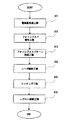
以下、電極の形成工程を音叉腕120,130を中心に説明する。また、音叉腕130は音叉腕120と同様のため、以下の説明は、音叉腕120の説明のみとする。図16は電極形成工程を示す概略フローチャートである。図17は、音叉腕120に電極が形成される工程を示す概略図である。
The tuning-fork type
First, the quartz substrate is etched or the like to form a tuning fork type crystal vibrating piece in which the electrode of FIG. 14 is not formed. Thereafter, an electrode is formed on the tuning-fork type quartz vibrating piece.
Hereinafter, the electrode forming process will be described focusing on the
先ず、図17(a)は、上記エッチングにより外形が形成された状態の音叉型水晶振動片の音叉腕120の図14のB−B’線概略断面図である。図17(a)に示すように、音叉腕120の表面120e及び裏面120fには、溝部120a、120aが形成される(溝部形成工程)。このような音叉腕120等を含む振動片全体にスパッタ等により金属膜である電極膜150を形成する(金属膜形成工程、図16のST1)。この状態を示したのが図17(b)である。図17に示す電極膜150は、下層がCrで厚みが例えば100Å乃至1000Åで形成される。そして、上層がAuで厚みが例えば500Å乃至1000Åで形成されている。
First, FIG. 17 (a) is a diagram 1 4 line B-B 'sectional view of the
このように表面全体に電極膜150を形成した後、図16のST2に示すようにフォトレジストを霧状に噴霧して電極膜150の上の全面に塗布する。すなわち、図17(c)に示すようにフォトレジスト膜151を形成する(フォトレジスト層形成工程)。
このフォトレジストは紫外光に感光感度を持つ樹脂をベースとした化合物であり、流動性を有するため、例えばスプレーにより霧状に噴霧して塗布される。
また、フォトレジスト膜151の厚みは、例えば1μm乃至6μmとなっている。
After the
This photoresist is a compound based on a resin having photosensitivity to ultraviolet light, and has fluidity, so that it is applied in the form of a mist by spraying, for example.
The thickness of the
次に、図16のST3に示すようにフォトレジストパターン形成を行う。すなわち、図14の電極形成部分(斜線部分)を除く部分を覆うような図示しないマスクを介して紫外線をフォトレジスト膜151に照射して(露光)、現像液で取り除き、加熱工程等を経てフォトレジスト膜151を固化させる。
これにより、図14の電極形成部分(斜線部分)に対応する形状のフォトレジストパターン152が形成される。
Next, as shown in ST3 of FIG. 16, a photoresist pattern is formed. That is, ultraviolet light is irradiated to the photoresist film 151 (exposure) through a mask (not shown) that covers a portion excluding the electrode forming portion (shaded portion) in FIG. The resist
Thereby, a
このとき、フォトレジストパターン152は、図14及び図15の短絡防止用間隔W1、具体的は例えば15μmの幅でフォトレスト膜151が形成されていない部分ができる。
ところで、フォトレジストは、上述のように電極膜150上に塗布されるが、図17(a)の音叉腕120の角部であるエッジ部分(図における矢印E)をカバーするように塗布する必要がある。このとき、塗布するフォトレジストが粒子状になっていた方がエッジ部分Eのカバーが良い。
しかしながらフォトレジストをこのように粒子状のものを含んだ状態で塗布すると、フォトレジスト現像後のフォトレジストパターン152の外形は正確な略直線ではなく、粒子の外形に沿った略波線に形成されてしまう。
このようにフォトレジストパターン152の外形線が、不均一であると前記短絡防止用間隔W1が15μmという微細な間隔を形成する場合、部分的に間隔が保持されないおそれがある。
間隔が保持されていない部分は、エッチングされない部分となってしまうため、電極同士の短絡等のおそれがある。
At this time, the
By the way, although the photoresist is applied on the
However, when the photoresist is applied in such a state that includes particles, the outer shape of the
As described above, when the outline of the
Since the portion where the interval is not maintained becomes a portion which is not etched, there is a risk of short-circuiting between the electrodes.
そのため、本実施の形態では、図16のST4に示すようにレーザ照射を行う(パターン形状調整工程)。具体的には、前記フォトレジストパターン152の一部の形状である図14の音叉腕120の腕表面120eの短絡防止用間隔W1について行われる。
すなわち、図18(a)に示すように、フォトレジストパターン152の外形線が不均一となり、このフォトレジストパターンをマスクとしてエッチングした場合、形成される溝電極120bと側面電極120dとが短絡等を生じないように、短絡防止用間隔W1が例えば15μm確保できるようにフォトレジストパターン152の外形がレーザによって調整される。
Therefore, in this embodiment, laser irradiation is performed as shown in ST4 of FIG. 16 (pattern shape adjustment step). Specifically, the shorting prevention interval W1 of the
That is, as shown in FIG. 18A, the outline of the
このレーザは、例えば、YAGレーザ等が用いられ、特にYAGレーザの3倍高調波を用いるとフォトレジストパターン152の外形をより正確に調整することができる。このようにフォトレジストパターン152を形成してからレーザを照射するので、特にフォトレジストの感光を防止するイエロールーム内でレーザを照射する必要がないので製造コストを低減することができる。また、レーザの照射は、図18(a)(b)に示すように音叉腕120の腕表面120eの短絡防止用間隔W1と腕裏面120fの短絡防止用間隔W1とを別々に行う。
As this laser, for example, a YAG laser or the like is used, and in particular, when the third harmonic of the YAG laser is used, the outer shape of the
しかし、これに限らず図18(c)に示すように腕表面120e及び腕裏面の120fの双方を同時にレーザによって加工することもできる。
この場合、生産工程を減らすことができるので生産コストも下げることができる
However, the present invention is not limited to this, and both the
In this case, production costs can be reduced because production processes can be reduced.
このようにフォトレジストパターン152がレーザによって正確に形成された後、図16のST5のエッチング工程となる(電極膜形成工程)。
具体的には、上述のフォトレジストパターン152をマスクとして電極膜150をエッチングにより除去する。
図19(a)は、エッチングにより電極膜150が除去された状態を示す図である。図19(a)に示すように本実施の形態の製造方法によれば、短絡防止用間隔W1を正確に確保することができる。
After the
Specifically, the
FIG. 19A shows a state where the
次に、図16のST6のレジスト剥離工程でフォトレジストパターン152を除去すれば、図19(b)に示すように溝電極120b、側面電極120dが正確に形成されることになる(フォトレジストパターン剥離工程)。
このとき、上述のレーザ照射工程(ST3)の図17に示すレーザ照射で電極膜150の一部が溶解し、この溶解した電極膜150の一部がレジストパターン152と共に除去されるので、より正確に短絡防止用間隔W1を形成することができる。
そして、このとき、音叉型水晶振動片100全体については、図14に示すように基部電極140a等が所定の形状で形成され、音叉型水晶振動片100の電極配置が終了する。
このようにして製造された音叉型水晶振動片100は、音叉腕120、130の腕表面120e、130e及び腕裏面120f、130fの短絡防止用間隔W1が例えば15μmに正確保持され、溝電極120b、130bと側面電極120d、130dとが短絡等することを有効に防止することができ、不良が生じにくい音叉型水晶振動片となる。
Next, if the
At this time, a part of the
At this time, with respect to the entire tuning fork type
In the tuning fork type
以上説明したように、本発明によれば、基部を短くしてもCI値の振動片素子間のバラツキが安定すると共に振動片全体も小型化できる振動片を有する振動子、この振動子を備える発振器及び電子機器を提供することができる。 As described above, according to the present invention, the oscillator having a resonator element can be miniaturized even entire vibrating piece with variations between vibrating piece element CI value is also a shorter base is stabilized, provided with the vibrator An oscillator and an electronic device can be provided.
100・・・音叉型水晶振動片
110・・・基部
111・・・固定領域
121、122・・・音叉腕
123,124・・・溝部
125・・・切り込み部
200・・・セラミックパッケージ音叉振動子
210・・・パッケージ
211・・・ベース部
212・・・側面部
213・・・蓋体
214・・・パッケージ側電極
300・・・デジタル携帯電話
400・・・音叉水晶発振器
410・・・集積回路
500・・・シリンダータイプ音叉振動子
510・・・リード
520・・・ステム
530・・・キャップ
DESCRIPTION OF
Claims (24)
前記基部から突出して形成され、その表面部及び/又は裏面部に溝部が形成されている振動腕部を有し、 It has a vibrating arm part that protrudes from the base part and has a groove part formed on its front and / or back part,
前記溝部内に溝電極が形成され、 A groove electrode is formed in the groove,
前記振動腕部の側面に側面電極が形成されている振動片の製造方法であって、 A method of manufacturing a resonator element in which a side electrode is formed on a side surface of the vibrating arm part,
前記振動片に電極膜を形成する電極膜形成工程と、An electrode film forming step of forming an electrode film on the vibrating piece;
前記溝電極と前記側面電極とをパターニングするためのレジストパターンを形成するレジストパターン形成工程と、 A resist pattern forming step of forming a resist pattern for patterning the groove electrode and the side electrode;
前記レジストパターン形成工程で前記レジストパターンにより形成された短絡防止用間隔を調整するために、前記レジストパターンの外形に対してレーザを照射するパターン形状調整工程と、In order to adjust the short-circuit prevention interval formed by the resist pattern in the resist pattern forming step, a pattern shape adjusting step of irradiating a laser to the outer shape of the resist pattern;
前記レジストパターンをマスクとして前記電極膜をエッチングし、前記溝電極と前記側面電極を形成する工程と、を有することを特徴とする振動片の製造方法。Etching the electrode film using the resist pattern as a mask to form the groove electrode and the side electrode.
前記レジストパターン形成工程で、前記レジストパターンで成る前記表面部及び前記裏面部の前記短絡防止用間隔を調整するために、一の前記レーザを前記表面部及び裏面部に形成された前記レジストパターンに同時に照射することを特徴とする請求項1又は2記載の振動片の製造方法。 The groove portion is formed on the front surface portion and the back surface portion of the vibrating arm portion,
Wherein the resist pattern formation step, in order to adjust the pre-Symbol said surface portion and said short-circuit prevention for spacing the rear surface portion made of a resist pattern, the resist pattern formed an the laser to the surface portion and the back surface The method for manufacturing a resonator element according to claim 1 , wherein the irradiation is performed simultaneously .
前記基部から突出して形成され、その表面部及び/又は裏面部に溝部が形成されている振動腕部を有し、 It has a vibrating arm part that protrudes from the base part and has a groove part formed on its front and / or back part,
前記溝部内に溝電極が形成され、 A groove electrode is formed in the groove,
前記振動腕部の側面に側面電極が形成されている振動片がパッケージ内に収容されている振動子の製造方法であって、 A vibrator manufacturing method in which a resonator element in which a side electrode is formed on a side surface of the vibrating arm portion is housed in a package,
前記振動片に電極膜を形成する電極膜形成工程と、An electrode film forming step of forming an electrode film on the vibrating piece;
前記溝電極と前記側面電極とをパターニングするためのレジストパターンを形成するレジストパターン形成工程と、 A resist pattern forming step of forming a resist pattern for patterning the groove electrode and the side electrode;
前記レジストパターン形成工程で前記レジストパターンにより形成された短絡防止用間隔を調整するために、前記レジストパターンの外形に対してレーザを照射するパターン形状調整工程と、In order to adjust the short-circuit prevention interval formed by the resist pattern in the resist pattern forming step, a pattern shape adjusting step of irradiating a laser to the outer shape of the resist pattern;
前記レジストパターンをマスクとして前記電極膜をエッチングし、前記溝電極と前記側面電極を形成する工程と、を有することを特徴とする振動子の製造方法。Etching the electrode film using the resist pattern as a mask to form the groove electrode and the side electrode.
前記基部から突出して形成され、その表面部及び/又は裏面部に溝部が形成されている振動腕部を有し、 It has a vibrating arm part that protrudes from the base part and has a groove part formed on its front and / or back part,
前記溝部内に溝電極が形成され、 A groove electrode is formed in the groove,
前記振動腕部の側面に側面電極が形成されている振動片と集積回路がパッケージ内に収容されている発振器の製造方法であって、 A method of manufacturing an oscillator in which a resonator element having a side electrode formed on a side surface of the vibrating arm portion and an integrated circuit are housed in a package,
前記振動片に電極膜を形成する電極膜形成工程と、An electrode film forming step of forming an electrode film on the vibrating piece;
前記溝電極と前記側面電極とをパターニングするためのレジストパターンを形成するレジストパターン形成工程と、 A resist pattern forming step of forming a resist pattern for patterning the groove electrode and the side electrode;
前記レジストパターン形成工程で前記レジストパターンにより形成された短絡防止用間隔を調整するために、前記レジストパターンの外形に対してレーザを照射するパターン形状調整工程と、In order to adjust the short-circuit prevention interval formed by the resist pattern in the resist pattern forming step, a pattern shape adjusting step of irradiating a laser to the outer shape of the resist pattern;
前記レジストパターンをマスクとして前記電極膜をエッチングし、前記溝電極と前記側面電極を形成する工程と、を有することを特徴とする発振器の製造方法。Etching the electrode film using the resist pattern as a mask to form the groove electrode and the side electrode.
前記基部から突出して形成され、その表面部及び/又は裏面部に溝部が形成されている振動腕部を有し、 It has a vibrating arm part that protrudes from the base part and has a groove part formed on its front and / or back part,
前記溝部内に溝電極が形成され、 A groove electrode is formed in the groove,
前記振動腕部の側面に側面電極が形成されている振動片であり、この振動片がパッケージ内に収容されている振動子であり、この振動子を制御部に接続して用いている電子機器の製造方法であって、 An electronic device in which a side electrode is formed on a side surface of the vibrating arm portion, the vibrator is a vibrator housed in a package, and the vibrator is connected to a control unit. A manufacturing method of
前記振動片に電極膜を形成する電極膜形成工程と、An electrode film forming step of forming an electrode film on the vibrating piece;
前記溝電極と前記側面電極とをパターニングするためのレジストパターンを形成するレジストパターン形成工程と、 A resist pattern forming step of forming a resist pattern for patterning the groove electrode and the side electrode;
前記レジストパターン形成工程で前記レジストパターンにより形成された短絡防止用間隔を調整するために、前記レジストパターンの外形に対してレーザを照射するパターン形状調整工程と、In order to adjust the short-circuit prevention interval formed by the resist pattern in the resist pattern forming step, a pattern shape adjusting step of irradiating a laser to the outer shape of the resist pattern;
前記レジストパターンをマスクとして前記電極膜をエッチングし、前記溝電極と前記側面電極を形成する工程と、を有することを特徴とする電子機器の製造方法。Etching the electrode film using the resist pattern as a mask to form the groove electrode and the side electrode.
Priority Applications (1)
| Application Number | Priority Date | Filing Date | Title |
|---|---|---|---|
| JP2004182630A JP4063255B2 (en) | 2000-12-25 | 2004-06-21 | Vibrating piece manufacturing method, vibrator manufacturing method, oscillator manufacturing method, and electronic device manufacturing method |
Applications Claiming Priority (2)
| Application Number | Priority Date | Filing Date | Title |
|---|---|---|---|
| JP2000392934 | 2000-12-25 | ||
| JP2004182630A JP4063255B2 (en) | 2000-12-25 | 2004-06-21 | Vibrating piece manufacturing method, vibrator manufacturing method, oscillator manufacturing method, and electronic device manufacturing method |
Related Parent Applications (1)
| Application Number | Title | Priority Date | Filing Date |
|---|---|---|---|
| JP2001392904A Division JP2002261575A (en) | 2000-12-25 | 2001-12-25 | Vibrating piece, vibrator, oscillator and electronic equipment |
Publications (3)
| Publication Number | Publication Date |
|---|---|
| JP2004266873A JP2004266873A (en) | 2004-09-24 |
| JP2004266873A5 JP2004266873A5 (en) | 2005-07-07 |
| JP4063255B2 true JP4063255B2 (en) | 2008-03-19 |
Family
ID=33133403
Family Applications (1)
| Application Number | Title | Priority Date | Filing Date |
|---|---|---|---|
| JP2004182630A Expired - Fee Related JP4063255B2 (en) | 2000-12-25 | 2004-06-21 | Vibrating piece manufacturing method, vibrator manufacturing method, oscillator manufacturing method, and electronic device manufacturing method |
Country Status (1)
| Country | Link |
|---|---|
| JP (1) | JP4063255B2 (en) |
Families Citing this family (1)
| Publication number | Priority date | Publication date | Assignee | Title |
|---|---|---|---|---|
| DE102007028288B4 (en) * | 2007-06-20 | 2013-06-06 | Epcos Ag | Acoustic wave MEMS device and method of manufacture |
-
2004
- 2004-06-21 JP JP2004182630A patent/JP4063255B2/en not_active Expired - Fee Related
Also Published As
| Publication number | Publication date |
|---|---|
| JP2004266873A (en) | 2004-09-24 |
Similar Documents
| Publication | Publication Date | Title |
|---|---|---|
| JP2013165529A (en) | Vibration piece, vibrator, oscillator and electronic apparatus | |
| US6894428B2 (en) | Vibrating piece, vibrator, oscillator, and electronic device | |
| JP3931662B2 (en) | Vibrating piece, vibrator, oscillator and electronic device | |
| JP2002261575A (en) | Vibrating piece, vibrator, oscillator and electronic equipment | |
| JP4694953B2 (en) | Piezoelectric vibrating piece manufacturing method, piezoelectric vibrating piece, piezoelectric vibrator, oscillator, electronic device, and radio timepiece | |
| TWI516027B (en) | Piezoelectric vibrating reed, piezoelectric vibrator, oscillator, electronic device, radio-controlled clock, and method for manufacturing piezoelectric vibrating reed | |
| TWI501056B (en) | Piezoelectric vibrating reed, piezoelectric vibrator, oscillator, electronic device, radio-controlled clock, and method for manufacturing piezoelectric vibrating reed | |
| JP4063255B2 (en) | Vibrating piece manufacturing method, vibrator manufacturing method, oscillator manufacturing method, and electronic device manufacturing method | |
| JP2008029030A (en) | Vibrator, oscillator, and electronic apparatus | |
| JP2004266871A5 (en) | ||
| JP2004266871A (en) | Vibrating piece, vibrator, oscillator, and electronic equipment | |
| JP2004266873A5 (en) | ||
| US20120217218A1 (en) | Piezoelectric vibrating reed, piezoelectric vibrating reed manufacturing method, piezoelectric vibrator, oscillator, electronic device and radio timepiece | |
| JP2004266872A (en) | Oscillating piece, vibrator, oscillator, and electronic equipment | |
| JP2004266872A5 (en) | ||
| JP2012080243A (en) | Piezoelectric vibrating piece manufacturing method, wafer, piezoelectric vibrator, oscillator, electronic equipment, and radio-controlled clock | |
| US8013498B2 (en) | Electronic device having a piezoelectric vibrating reed with a discontinuous electrode film | |
| JP5885523B2 (en) | Method for manufacturing piezoelectric vibrating piece | |
| JP6105648B2 (en) | Piezoelectric vibrating piece, piezoelectric vibrator, oscillator, electronic device, radio timepiece, and method of manufacturing piezoelectric vibrating piece | |
| JP2013021601A (en) | Piezoelectric vibrating piece, method for manufacturing piezoelectric vibrating piece, piezoelectric vibrator, oscillator, electronic appliance, and radio-controlled timepiece | |
| JP5246701B2 (en) | Method for manufacturing piezoelectric vibrating piece | |
| JP2005184665A (en) | Method of manufacturing piezoelectric substrate, piezoelectric vibrating element, piezoelectric vibrator, and piezoelectric oscillator |
Legal Events
| Date | Code | Title | Description |
|---|---|---|---|
| A521 | Written amendment |
Free format text: JAPANESE INTERMEDIATE CODE: A523 Effective date: 20041227 |
|
| A621 | Written request for application examination |
Free format text: JAPANESE INTERMEDIATE CODE: A621 Effective date: 20041227 |
|
| RD04 | Notification of resignation of power of attorney |
Free format text: JAPANESE INTERMEDIATE CODE: A7424 Effective date: 20070507 |
|
| RD02 | Notification of acceptance of power of attorney |
Free format text: JAPANESE INTERMEDIATE CODE: A7422 Effective date: 20070611 |
|
| A131 | Notification of reasons for refusal |
Free format text: JAPANESE INTERMEDIATE CODE: A131 Effective date: 20070703 |
|
| A521 | Written amendment |
Free format text: JAPANESE INTERMEDIATE CODE: A523 Effective date: 20070827 |
|
| TRDD | Decision of grant or rejection written | ||
| A01 | Written decision to grant a patent or to grant a registration (utility model) |
Free format text: JAPANESE INTERMEDIATE CODE: A01 Effective date: 20071211 |
|
| A61 | First payment of annual fees (during grant procedure) |
Free format text: JAPANESE INTERMEDIATE CODE: A61 Effective date: 20071224 |
|
| R150 | Certificate of patent or registration of utility model |
Free format text: JAPANESE INTERMEDIATE CODE: R150 |
|
| FPAY | Renewal fee payment (event date is renewal date of database) |
Free format text: PAYMENT UNTIL: 20110111 Year of fee payment: 3 |
|
| FPAY | Renewal fee payment (event date is renewal date of database) |
Free format text: PAYMENT UNTIL: 20110111 Year of fee payment: 3 |
|
| FPAY | Renewal fee payment (event date is renewal date of database) |
Free format text: PAYMENT UNTIL: 20120111 Year of fee payment: 4 |
|
| FPAY | Renewal fee payment (event date is renewal date of database) |
Free format text: PAYMENT UNTIL: 20120111 Year of fee payment: 4 |
|
| FPAY | Renewal fee payment (event date is renewal date of database) |
Free format text: PAYMENT UNTIL: 20130111 Year of fee payment: 5 |
|
| FPAY | Renewal fee payment (event date is renewal date of database) |
Free format text: PAYMENT UNTIL: 20130111 Year of fee payment: 5 |
|
| FPAY | Renewal fee payment (event date is renewal date of database) |
Free format text: PAYMENT UNTIL: 20140111 Year of fee payment: 6 |
|
| LAPS | Cancellation because of no payment of annual fees |