JP4051741B2 - Optical scanning device - Google Patents
Optical scanning device Download PDFInfo
- Publication number
- JP4051741B2 JP4051741B2 JP34950497A JP34950497A JP4051741B2 JP 4051741 B2 JP4051741 B2 JP 4051741B2 JP 34950497 A JP34950497 A JP 34950497A JP 34950497 A JP34950497 A JP 34950497A JP 4051741 B2 JP4051741 B2 JP 4051741B2
- Authority
- JP
- Japan
- Prior art keywords
- mirror
- sub
- scanning direction
- light beam
- optical system
- Prior art date
- Legal status (The legal status is an assumption and is not a legal conclusion. Google has not performed a legal analysis and makes no representation as to the accuracy of the status listed.)
- Expired - Fee Related
Links
Images


Landscapes
- Laser Beam Printer (AREA)
- Mechanical Optical Scanning Systems (AREA)
Description
【0001】
【発明の属する技術分野】
本発明は、光走査装置に係り、より詳しくは、光ビームを回転多面鏡によって所定の主走査方向に偏向し、偏向された光ビームで被走査面を走査する光走査装置に関する。
【0002】
【従来の技術】
従来よりデジタル複写機やレーザビームプリンタ等の画像形成装置に使用される光走査装置としては、形成される画像のデジタル画像データに基づき変調された光ビームを、例えば回転多面鏡等の反射型の偏向器により反射して偏向した後、例えばfθレンズ等の結像レンズにより被走査面上にスポットとして集光させて画像書き込みを行うものが広く用いられている。なお、fθレンズとは、回転多面鏡により等角速度で偏向された光ビームを、被走査面上に等速度で走査させるべく屈折させるレンズである。
【0003】
従来の具体的な構成としては、6〜10面の回転多面鏡を、回転数が8000〜20000rpm(=回転数/分)のモータにより駆動するものが一般的であるが、近年、画像形成装置には、高画質でしかも高速なアウトプットが強く求められており、上記の回転多面鏡及びモータの構成では対応しきれなくなっている。
【0004】
ところで、高画質化を実現するには、高密度での書き込み(高解像度化)が最も有効な手段であるが、書き込み画像を高密度化するには、光ビームが被走査面を走査する主走査方向では、デジタル画像データに基づく光ビームの変調速度を高速化し、副走査方向では、単位時間に書き込む本数を増やすことが必要となる。
【0005】
また、高速なアウトプットを実現するには、画像形成装置のプロセススピード(一般には用紙を搬送する速度)を上げることが有効な手段となる。但し、プロセススピードが上がると光走査装置からみて被走査媒体(例えば感光体ドラム等)の周速が上がるため、プロセススピードにほぼ比例して、光走査装置の書き込み速度を上げる必要がある。
【0006】
すなわち、高画質で且つ高速なアウトプットという要求を満足するには、光走査装置は単位時間当たりの書き込みライン数を急激に増加させなければならない。例えば、書き込み密度が1.5倍(400dpi→600dpi)、アウトプットスピードが1.5倍になると、光走査装置の書き込み速度(=書き込み本数/時間)は、2.25倍(=1.5×1.5)必要となる。
【0007】
これに対し、光走査装置の書き込み速度を上げる方法としては、回転多面鏡を駆動するモータの回転数を増す、回転多面鏡の面数を増やす、光ビームをマルチ化するなどの方法が従来より提案されている。
【0008】
ところが、回転多面鏡駆動用モータの回転数を過度に上げると、モータの負荷が大きくなり、消費電力の増加だけでなく故障率の増大という問題(1)を引き起こす。
【0009】
また、回転多面鏡の面数を増やすと、回転多面鏡が大型化するためモータの負荷が増大し、上記と同様に消費電力の増加及び故障率の増加という問題(2)を引き起こす。なお、回転多面鏡の大型化は、回転多面鏡へ入射する光ビームを、回転多面鏡の回転角によらず反射面からはみだすことなく偏向するという制約によって、回転多面鏡の各面の面幅が決定されるために生じる。
【0010】
更に、光ビームのマルチ化は、複数の発光点を有する光源又は複数の光源から発せられる光ビームを高精度に合成する複雑な光学系が必要となり、装置が高価になるという問題(3)がある。
【0011】
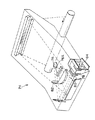
上記(1)〜(3)の問題を解決するものとして、特開平8−171069号公報に示す技術が知られており、図8はこの公報に開示された光走査装置74の概略構成図である。
【0012】
この図8に示す光走査装置74では、回転多面鏡76の反射面76Aの主走査方向面幅より広い幅のレーザビームを反射面76Aに照射するオーバーフィルド(Overfilled)方式の光学系を採用することで、回転多面鏡76の回転数を上げることなく、かつ回転多面鏡76を大径化することなく、高解像度化および高速化を実現している。
【0013】
また、回転多面鏡76に光ビームを入射するための第1の光学系を、コリメータレンズ78、シリンドリカルレンズ80、凸レンズ82の順に配置し、光源84をコリメータレンズ78の焦点位置より内側に配置して発散光とすることにより、光源84から回転多面鏡76までの光路長を短縮するとともに、偏向角を±15°より大きくとることにより、これ以前に提案されたオーバーフィルド方式の光学系を含む光走査装置に比べて装置の小型化を実現している。
【0014】
【発明が解決しようとする課題】
しかしながら、回転多面鏡による光ビームの偏向角は回転多面鏡の面数に大きく依存し、有効走査率(回転多面鏡が偏向可能な最大角度に対する、画像書き込みに使用する角度の比率)を上げても、回転多面鏡の多面化とともに結像光学系の焦点距離が長くなることは避け難い。
【0015】
また、特開平8−171069号公報に開示された光走査装置の第2の結像光学系は、2枚のレンズを組み合わせたfθレンズとシリンドリカルミラーにより構成されているため、光学部品が高価であるとともに、回転多面鏡から被走査面までの光路上でシリンドリカルミラーを配置する位置とシリンドリカルミラーによる折り返し角度(副走査断面での入射角)とが結像性能に直接影響するため、光路のレイアウト自由度は低いといわざるを得ない。
【0016】
本発明は、上記問題点を解消するために成されたものであり、高速・高画質を実現し、且つ小型で低コストな光走査装置を提供することを第1の目的とする。また、本発明は、光路を複数回折り返した光走査装置において、加工誤差、組み立て誤差による性能劣化を最小化することができる光走査装置を提供することを第2の目的とする。
【0017】
【課題を解決するための手段】
上記第1の目的を達成するために、請求項1記載の光走査装置は、光源と、所定の回転軸の回りを略等角速度で回転し且つ前記回転軸に平行な複数の反射面が外周に形成され、入射された光ビームを前記反射面により偏向させる回転多面鏡と、光源から射出された光ビームを、前記回転軸に平行な副走査方向に収束させて前記反射面上に前記副走査方向に垂直な主走査方向に沿った線像として結像させる第1の結像光学系と、前記副走査方向に沿った断面内で前記反射面と被走査面とを略共役な結像関係とするとともに、前記反射面により偏向された光ビームを、等速度で前記被走査面を走査するスポットとして結像させる第2の結像光学系と、前記回転多面鏡から前記第2の結像光学系に至る光路上に配置され且つ前記副走査方向に沿った断面で90°の相対角度を成す第1のミラー対と、前記第2の結像光学系から前記被走査面に至る光路上に配置され且つ前記副走査方向に沿った断面で90°の相対角度を成す第2のミラー対と、を有し、前記第2の結像光学系は単玉のプラスチック非球面レンズにより構成され、前記副走査方向に沿った断面内での前記反射面と前記被走査面との結像関係に係る共役倍率βが、1.5<β<3.5を満足し、前記光ビームは、前記回転多面鏡の反射面に、該反射面の主走査方向に沿った面幅より広い光ビ−ムとして入射することを特徴とする。
【0018】
一方、請求項2記載の光走査装置は、光源と、所定の回転軸の回りを略等角速度で回転し且つ前記回転軸に平行な複数の反射面が外周に形成され、入射された光ビームを前記反射面により偏向させる回転多面鏡と、光源から射出された光ビームを、前記回転軸に平行な副走査方向に収束させて前記反射面上に前記副走査方向に垂直な主走査方向に沿った線像として結像させる第1の結像光学系と、前記副走査方向に沿った断面内で前記反射面と被走査面とを略共役な結像関係とするとともに、前記反射面により偏向された光ビームを、等速度で前記被走査面を走査するスポットとして結像させる第2の結像光学系と、前記回転多面鏡から前記第2の結像光学系に至る光路上に配置され且つ前記副走査方向に沿った断面で90°の相対角度を成す第1のミラー対と、前記第2の結像光学系から前記被走査面に至る光路上に配置され且つ前記副走査方向に沿った断面で90°の相対角度を成す第2のミラー対と、を有し、前記第1のミラー対は、前記第1の結像光学系からの光ビームが入射し、該第1のミラー対で折り返されて所定の平面ミラーで反射し、反射した光ビームが再度該第一のミラー対に第一回目と逆方向に入射し、該第1のミラー対で折り返されて前記回転多面鏡の反射面に入射するように、配置されることを特徴とする。
【0020】
上記第2の目的を達成するために、請求項3記載の光走査装置では、請求項2に記載の光走査装置において、前記平面ミラーは、前記回転多面鏡の回転軸と平行な所定の軸の回りに回転可能であり、且つ前記所定の軸と前記回転多面鏡の反射面の法線とを含む平面内で、前記所定の軸回りの回転と独立に回転可能に設けられていることを特徴とする。
【0021】
また、請求項4記載の光走査装置では、請求項1乃至請求項3の何れか一項に記載の光走査装置において、前記光源は、射出される光ビームの光軸に直交する平面内で、前記主走査方向に対応する方向及び前記副走査方向に対応する方向にそれぞれ独立に移動可能に設けられていることを特徴とする。
【0022】
また、請求項5記載の光走査装置では、請求項1乃至請求項4の何れか一項に記載の光走査装置において、前記第2のミラー対は、前記副走査方向に沿った断面内で回転可能及び平行移動可能に設けられることを特徴とする。
【0023】
また、請求項6記載の光走査装置では、請求項1乃至請求項5の何れか一項に記載の光走査装置において、前記第2のミラー対は、該第2のミラー対の各ミラーの反射面を延長した平面同士が交わって形成される直線上の固定点で固定されることを特徴とする。
【0025】
上記請求項1及び請求項2記載の光走査装置では、光源から射出された光ビームは第1の結像光学系に入射され、第1の結像光学系は、光ビームを副走査方向に収束させて回転多面鏡の反射面上に副走査方向に垂直な主走査方向に沿った線像として結像させる。回転多面鏡は、所定の回転軸の回りを略等角速度で回転し、外周に形成された反射面により光ビームを偏向させる。そして、回転多面鏡により偏向された光ビームは第2の結像光学系に入射される。この第2の結像光学系は、副走査方向に沿った断面内で回転多面鏡の反射面と被走査面とを略共役な結像関係とするとともに、入射してきた光ビーム(=主走査方向に沿った線像として回転多面鏡の反射面に結像し該反射面で偏向された光ビーム)を、等速度で被走査面を走査するスポットとして被走査面に結像させる。
【0026】
上記光走査装置としては、図9に示すオーバーフィルド走査光学系90を含む光走査装置を例示することができる。この図9は、単玉のfθレンズ17を含むオーバーフィルド走査光学系90の平面図(展開図)である。ここで例えば、回転多面鏡16は12個の反射面を有し内接径が25mmとされており、該回転多面鏡16による走査幅L1はA3の短辺サイズ(297mm)に対応している。回転多面鏡16の反射面から回転多面鏡側レンズ面17Aまでの距離は135mm、fθレンズ17の中心厚は20mm、被走査面側レンズ面17Bから被走査面20Aまでの距離は360mmとされている。
【0027】
なお、fθレンズ17は、光学設計上、単玉で十分な結像性能を得ようとすると大型化する傾向があるが、プラスチックレンズの採用により、低コストを実現できる。また、回転多面鏡16へ入射する第1の結像光学系の主光線と第2の結像光学系(fθレンズ17)の光軸の成す角度は、35°であり、偏向走査中の反射面に隣接する反射面へ溢れ出て該隣接する反射面で反射した光ビームが光源11に戻らない角度に設定してある。
【0028】
上記のような光学系を小型な筐体に実装するために、請求項1及び請求項2記載の光走査装置では、副走査方向に沿った断面で90°の相対角度を成すミラー対を、回転多面鏡から第2の結像光学系に至る光路上及び第2の結像光学系から被走査面に至る光路上のそれぞれに配置している。なお、回転多面鏡から第2の結像光学系に至る光路上に配置されたミラー対を第1のミラー対と称し、第2の結像光学系から被走査面に至る光路上に配置されたミラー対を第2のミラー対と称する。
【0029】
上記第1のミラー対や第2のミラー対のように、副走査方向に沿った断面で90°の相対角度を成すミラー対は、図10(A)に示すように、光ビームを折り曲げることができ、このようなミラー対を光路上に配置することで、実装上の光路長を、展開した状態の約半分に縮めることができる。
【0030】
なお、光ビームを折り曲げる構成としては、図10(B)に示すように1枚のミラー99で折り曲げる構成も考えられるが、この構成では、図10(A)に示すように2枚のミラー(ミラー対)98で折り曲げる場合よりも、高さ方向により広い空間が必要となり、光走査装置の小型化が困難となるおそれがある。
【0031】
図10(A)、(B)の例で、第1の結像光学系106の中心点と回転多面鏡104への光ビーム入射点との高さの差異を比較すると、光ビームをミラー対98で折り曲げる場合の高さの差異は10mmであるのに対し、光ビームをミラー99で折り曲げる場合の高さの差異は27.5mmとなる。即ち、2枚のミラー(ミラー対)で折り曲げる方が、1枚のミラーで折り曲げるよりも、光走査装置の小型化には効果がある。なお、図10(A)、(B)の各々に示した隙間J1は入射光ビームと出射光ビームとの干渉を防ぐために必要な隙間を表しており、隙間J2は第1の結像光学系106と回転多面鏡104とを上方から取り付けるために必要な隙間(約25mm)を表している。
【0032】
このように請求項1及び請求項2記載の発明では、構造が複雑で高価な光学系を用いることなく、90°の相対角度を成すミラー対を第2の結像光学系の前後にそれぞれ配置したので、回転多面鏡から被走査面に至る光路において光路の折り畳みが2回行われることになり、実装上の光路長を一気に短縮することができる。即ち、光走査装置の高さを抑制しながら、実装上の光路長を一気に短縮できるので、装置コストの高騰を回避しつつ光走査装置を小型化することができる。
【0033】
ここで、請求項1記載の発明では、第2の結像光学系は単玉のプラスチック非球面レンズにより構成されており、副走査方向に沿った断面内での反射面と被走査面との結像関係に係る共役倍率βが、1.5<β<3.5を満足するよう構成されている。
このように、第2の結像光学系を、廉価な単玉のプラスチック非球面レンズで構成することで、光走査装置の装置コストを低く抑えることができる。
また、副走査方向に沿った断面内での反射面と被走査面との結像関係に係る共役倍率βが1.5以下になると、単玉レンズでは十分な結像性能が得られないとともに、第2の結像光学系の前後に90°ミラー対を配置するスペースの確保が困難となる。また、共役倍率βが3.5以上になると、第2の結像光学系のレンズが大型化するとともに、光走査装置の筐体が大型化する。
従って、共役倍率βを1.5より大きく且つ3.5未満(即ち、1.5<β<3.5)に設定することにより、第2の結像光学系の前後に90°ミラー対を配置するための十分なスペースを確保しつつ単玉レンズでも良好な光学性能を得ることができ、第2の結像光学系のレンズの大型化を回避できる。即ち、高性能で且つ小型な光走査装置を提供することができる。
また、請求項1に記載したように、光ビームが回転多面鏡の反射面に該反射面の主走査方向に沿った面幅より広い光ビ−ムとして入射するよう構成されたオーバーフィルド方式では、前述したように有効走査率を上げても結像光学系の焦点距離が長くなるが、請求項1記載の発明を適用することにより、結像光学系の光路長が長くなっても実装上の光路長が長くなることを回避し、光走査装置の大型化を回避することができる。
一方、請求項2記載の発明のように、第一の結像光学系からの光ビームが第1のミラー対に入射し、該第1のミラー対で折り返されて所定の平面ミラーで反射し、そして、反射した光ビームが再度該第1のミラー対に第1回目と逆方向に入射し、該第1のミラー対で折り返されて回転多面鏡の反射面に入射するように、第1のミラー対を配置することが好ましい。
【0034】
このように第1の結像光学系から回転多面鏡までの光路を、折り曲げ且つ光ビームが第1のミラー対を2回通過するよう構成することで、上記回転多面鏡より前段の光学系の光路については、実装上の光路長を、展開した状態の約半分に縮めることができ、部品点数を増やすことなく比較的簡素な構成で光走査装置をさらに小型化することができる。
【0035】
回転多面鏡より後段の光学系の光路(回転多面鏡から被走査面に至る光路)については、前述したように第1のミラー対と第2のミラー対により光路の折り畳みが2回行われ、実装上の光路長が一気に短縮される。
【0036】
よって、請求項2記載の発明によれば、回転多面鏡より前段の光学系の光路と回転多面鏡より後段の光学系の光路の両方において、実装上の光路長が短縮され、光走査装置の小型化をより一層図ることができる。
【0038】
また、請求項3記載の発明では、平面ミラーが、回転多面鏡の回転軸と平行な所定の軸の回りに回転可能で且つ該所定の軸と回転多面鏡の反射面の法線とを含む平面内で、所定の軸回りの回転とは独立に回転可能に設けられている。
【0039】
このように2軸方向に回転可能な平面ミラーを、上記のように光源から回転多面鏡に至るまでに光ビームが2回通過するよう構成された第1のミラー対と組み合わせて配置することにより、第1のミラー対に入射する光ビームの入射角等に誤差があっても、組立・調整時に、光ビームが回転多面鏡の反射面に対し所望の位置に導光されるように、平面ミラーを2軸方向に回転させて位置調整することができる。
【0040】
また、請求項4記載の発明のように、光源を、射出される光ビームの光軸に直交する平面内で、主走査方向に対応する方向(以下、主走査対応方向と称する)及び副走査方向に対応する方向(以下、副走査対応方向と称する)にそれぞれ独立に移動可能に設けることが望ましい。これにより、組立・調整時に、第1のミラー対に入射する光ビームの入射角等の誤差が小さくなるように、光源を、主走査方向に対応する方向及び副走査方向に対応する方向にそれぞれ適宜移動させて光源位置を調整することができ、より高精度な光路調整が可能となる。
【0041】
また、請求項5記載の発明のように、第2のミラー対を、副走査方向に沿った断面内で回転可能及び平行移動可能に設けることが望ましい。これにより、組立・調整時に被走査面上の走査線の位置や結像倍率等を補正することができる。
【0042】
次に、請求項6記載の発明では、第2のミラー対は、該第2のミラー対の各ミラーの反射面を延長した平面同士が交わって形成される直線上の固定点で固定されている。
【0043】
ここで、第2のミラー対を、各ミラーの反射面を延長して形成される直線上の固定点で固定することにより、光路ずれが最小となる理由について説明する。
【0044】
図11は、第2のミラー対19が誤差により回転したときの光路を示した副走査断面図である。尚、第2のミラー対19への入射ビームIと、第2のミラー対19からの射出ビームOは、ともに紙面内にあるものとする。
【0045】
図11の破線ACBは、第2のミラー対19が理想的に取り付けられている状態を示しており、光ビームは、I→A→B→Oの光路を通る。実線A’CB’は、第2のミラー対19が、90°の相対角度を保ったまま、2つの反射面を延長して交わる直線Cの回りに回転した状態を示しており、光ビームはI→A’→B’→Oの光路を通る。
【0046】
ミラー19A上の点A’に立てた垂線をA’E、ミラー19B上の点B’に立てた垂線をB’F、2つの垂線の交点をDとすると、入射する光ビームI、射出する光ビームOはともに紙面内にあるので、反射の法則により以下の関係が求められる。
【0047】
∠IA’E=∠EA’B’ ・・・(1)
∠A’B’F=∠FB’O ・・・(2)
また、2枚のミラーの相対角度が保たれるとすると、
∠A’CB’=90° ・・・(3)
であり、∠EA’C、∠CB’Fはともに90°を成すので、四角形A’CB’Dは長方形となる。
【0048】
この長方形A’CB’Dの対角線A’B’と対角線CDの交点を交点Gとすると、三角形A’GDは二等辺三角形となり、
∠CDA’=∠EA’B’ ・・・(4)
となるから、式(1)、(4)より、
∠IA’E=∠CDA’ ・・・(5)
が得られ、
IA’//DC ・・・(6)
となる。即ち、交点Gは、点Cを通り入射ビームIA’に平行な直線上に位置する点となる。
【0049】
一方、入射する光ビームと90°ミラー19で反射され射出する光ビームとは、常に平行となるから、
IA’//B’O ・・・(7)
となり、結局、
IA’//DC//B’O ・・・(8)
となる。
【0050】
ここで、交点Gは、長方形A’DB’Cの対角線の交点であるから、
A’G=GB’ ・・・(9)
なる関係がある。
【0051】
式(8)、(9)より、点Gから直線IA’までの距離Laと、点Gから直線B’Oまでの距離Lbとは等しくなる。
【0052】
以上のことから、第2のミラー対19から射出される光ビームB’Oは、入射する光ビームIA’から、点Cを通りIA’に平行な直線までの距離の2倍の位置(点B’)から、入射光ビームIA’と平行に射出することになる。
【0053】
このように、90°の相対角度を成す第2のミラー対19が、2つの反射面を延長して交わる直線を中心として回転する場合、第2のミラー対19への入射ビームの位置が変わらなければ、射出ビームの射出位置は不変となる。
【0054】
これにより、第2のミラー対を保持するホルダーを、各ミラーの反射面を延長して形成される直線上の固定点で固定することにより、光路ずれを最小とすることができる。
【0055】
以上説明したように、被走査面への光ビームの入射角度等を調整するために使用可能な第2のミラー対を、各ミラーの反射面を延長して交わる直線上の固定点で固定することにより、調整完了後のネジ締結時に発生しうる第2のミラー対の位置ずれによる光ビームのアライメント変動を最小とし、良好な光学性能を得ることができる。
【0060】
【発明の実施の形態】
以下、本発明に係る各種の実施形態を説明する。
【0061】
[第1実施形態]
まず、本発明に係る第1実施形態を説明する。以下の各実施形態における光走査装置30の光学系の基本仕様は、前述した図9の構成と同様である。
【0062】
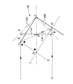
以下、図9、図1、図2(A)、(B)を参照しながら、光ビームの光路に沿って光走査装置30の概略構成を説明する。
【0063】
光源としての半導体レーザ11から射出した光ビームは、凸レンズ12により緩い収束光束とされたのち、シリンドリカルレンズ13により副走査対応方向に、より強く収束した光束となる。この光束は、90°の相対角度を成して筐体10に固定された第1のミラー対14(14A、14B)により折り返されて平面ミラー15に入射する。
【0064】
平面ミラー15は、反射光束を回転多面鏡16に向かわせるべく、回転多面鏡16の回転軸16Aと直交する平面(図1に示す平面)内で該平面ミラー15の法線Hが平面ミラー15への入射光ビームと角度θを成すように、配置されている。平面ミラー15により第1のミラー対14に戻された光束は、再度折り返されたのち、反射面16B近傍で線像となる収束状態で回転多面鏡16に入射する。このとき、隣接面からの戻り光束が光源11に戻らないように、回転多面鏡16への入射光ビームが回転多面鏡16による偏向中心に対し角度αを成すよう構成されている。
【0065】
回転多面鏡16は駆動モータ22により上方から見て時計回りに回転し、反射面16Bで偏向された走査光ビームは、第1のミラー対14に再々度入射する。ミラー対14により折り返された走査光ビームは、回転多面鏡16に対して筺体10の裏側に取り付けられ単玉非球面レンズで構成されたfθレンズ17に入射する。fθレンズ17から射出した光束は、ホルダー18に固定された第2のミラー対19(19A、19B)により折り返されて、感光ドラム20に至る。
【0066】
なお、走査光ビームのうち走査端に向かう光ビームは、第2のミラー対19を通過後にピックアップミラー21により折り曲げられて、図示しない同期検出センサー(SOSセンサー)へ導かれる。
【0067】
このように、90°折り返しミラー対14を第2の結像光学系(ここではfθレンズ17)の前に配置し且つ90°折り返しミラー対19を第2の結像光学系の後に配置することにより、筺体10の内部を光ビームがほぼ一回半往復し、展開状態では非常に長い光路長をもつ光学系を高密度実装状態で折り量むことができる。その結果、実装状態での占有長さ、すなわち筺体10の端面から感光ドラム20までの距離を展開状態の約1/2とし、且つ筺体10の高さが約80mmというコンパクトな光走査装置30を実現することができる。
【0068】
また、凸レンズ12およびシリンドリカルレンズ13より成る第1の結像光学系から射出した光ビームも第1のミラー対14を2回通過するよう構成することにより、光学系全体を小型な筺体内に実装可能となる。
【0069】
[第2実施形態]
次に、第2実施形態を説明する。ここでは、本発明の第2の目的に係る加工誤差・取り付け誤差の影響を最小とする調整について説明する。
【0070】
第1実施形態で述べた図1および図2に示した構成は、光走査装置の小型化を実現しているが、従来の光走査装置に比べ、光路上の反射回数が多くなっている。反射回数が増えると誤差の累積により、光学性能が劣化することが懸念される。そこで、第2実施形態では、光学部品の加工精度および取り付け精度を厳しくしコスト高となることを回避しつつ、ある程度の部品加工誤差、取り付け誤差を許容した上で、光走査装置全体として十分な光学性能を得る構成について説明する。
【0071】
具体的には、90°の相対角度を成すミラー対14と2軸調整機能をもった平面ミラー15とを組み含わせた調整構造について説明する。
【0072】
90°の相対角度を成すミラー対については、筺体の高さ方向のサイズを削減できる利点を既に述べたが、もうひとつ入射光線と射出光線との平行度を保存するという特徴がある。
【0073】
図3は、光源11から平面ミラー15までの光路を示した副走査断面図である。光ビーム、反射鏡14A、14B、15に誤差がなければ、ミラー対14を2回通過した光ビームは、入射ビームと同じ主走査平面内に戻る構成となっている。
【0074】
ここで、誤差がある場合について考える。誤差の要因としては、入射光ビームの位置(高さ)および角度と、光学部品の姿勢(取り付け角度)の二つが考えられる。
【0075】
図4(A)は、理想の部品取り付けが行われた90°ミラー対14および反射ミラー15に対し、誤差をもった光ビームが入射したときの光路を示す図である。90°ミラー対14を1回目に通過したとき、2回目に通過したとき、それぞれの過程では入射光ビームと射出光ビームの平行度は保たれている。
【0076】
ところが、2回の過程を1つと捉え、90°ミラー対14へ入射する光ビームと、90°ミラー対14から射出した光ビームとを比較すると、角度誤差の大きさは保存されるが方向が反対となるため、位置としては大きな誤差を生じ、最悪の場合、回転多面鏡16の反射面16Bから外れてしまい、調整機構無しでの実使用は困難である。
【0077】
そこで、第2実施形態では、上記問題に対し、図5(A)、(B)に示す2軸の調整機構を平面ミラー15に与えることにより、以下のようにして解決している。即ち、平面ミラー15は、その反射面15Aと同一平面内にある回転軸52を持つブラケット51に、固定ばね53により取り付けられている。反射面15Aは、ブラケット51が回転することにより、主走査面内で角度調整することができる。
【0078】
一方、反射面15Aの上端部付近には、イモネジ54が設けられており、このイモネジ54で煽りを加えることにより、反射面15Aは、副走査断面内で角度調整することができる。
【0079】
実際の調整では、例えば、副走査方向については、回転多面鏡16Bの直前に、光ビームの通過位置を検出するポジションセンサー(不図示)を設け、このポジションセンサーからの出力を検知しながら、イモネジ54を煽り反射面15Aの角度を調整することができる。調整後の光路の一例を図4(B)に示す。
【0080】
また、主走査方向についても同様に、設計値(いわゆるノミナル)からの光路ずれは発生するので、回転多面鏡16Bの直前に、光ビームのパワーを検出するパワーセンサー(不図示)を設け、反射面16Bとパワー分布との関係を検知しながらブラケット52を回転させて、適切な位置で平面ミラー15を筺体10に固定する。
【0081】
以上のように、90°の相対角度をもつミラー対14と2軸調整機能をもつ平面ミラー15とを組み合わせ、上記のような主走査方向、副走査方向に関する調整を行うことにより、部品の加工・取り付け誤差に起因する光路ずれを補正することができる。
【0082】
[第3実施形態]
次に、第3実施形態を説明する。一般的に、反射回数が多い光学系では、光路中の複数位置で光路ずれを検知し、調整することがより望ましい。これは、光ビームの位置誤差検出に比べ、角度誤差の検出が非常に難しいからである。
【0083】
そこで、第3実施形態では、図6(A)、(B)を参照して、本発明の構成に適用可能な、光路中の複数位置で光路ずれを調整する方法を述べる。調整は、光源11と平面ミラー15により行い、光路の位置検出は、第1のミラー対14への入射前の位置101と、回転多面鏡16の直前の位置102とで行う。
【0084】
まず、光源11を主走査対応方向(図6(B)の矢印M1、M2方向)および副走査対応方向(図6(A)の矢印S1、S2方向)に移動させて、第1のミラー対14への入射前の位置101での位置ずれを調整する。この結果、第1のミラー対14に入射する光ビームの誤差は概ね角度成分のみとなる。
【0085】
次に、前述した方法により平面ミラー15に対し、イモネジ54による反射面15Aの角度調整、及びブラケット52を回転させることによる平面ミラー15の位置調整を行うことにより、回転多面鏡16の直前の位置102での位置ずれを調整する。これにより、光源11から回転多面鏡16までの光路上で、設計値の光路から大きく外れる部分は無くなる。上記では、距離を隔てた2点(位置101、102)で位置ずれを調整しているので、1点で調整する場合に比べて、第2の結像光学系へ入射する光ビームの角度誤差も小さくでき、この点からも光学性能の劣化を抑制できる。
【0086】
次に、第2のミラー対19の固定方法について述べる。図7(A)、(B)は、第2のミラー対19の保持構造および筺体10への締結方法を説明するための図である。
【0087】
第2のミラー対19は、回転および平行移動により、感光ドラム20上での走査線の位置、斜め走査、倍率等を調整する働きを持っている。調整は治具上で行われるが、調整終了状態を崩すことなく強固に固定する必要がある。固定方法としては、ネジ締結が一般的であるが、ネジの締め付けトルクにより、せっかく調整した位置からずれて固定されてしまい、性能が劣化するおそれがある。
【0088】
そこで、本実施形態では、図7(B)に示すように、第2のミラー対19を構成するミラー19A、19Bの反射面をそれぞれ延長して交わる直線上の固定点71で、ホルダー18を筺体10に固定している。
【0089】
前述した原理により、各ミラーの反射面を延長して交わる直線上の固定点71でホルダー18を筺体10に固定したことで、調整完了後のネジ締結時に発生しうる第2のミラー対19の位置ずれによる光ビームのアライメント変動を最小とし、良好な光学性能を得ることができる。
【0090】
次に、第2の結像光学系(fθレンズ17)の望ましい構成について説明する。図1には、低コスト化を図るために、単玉非球面レンズをfθレンズ17に採用した構成例を示した。また、本発明の適用範囲としては、単玉非球面レンズに限定されるものではないが、ほぼ共役関係となっている回転多面鏡16の反射面16Bと感光ドラム20の被走査面との副走査断面における横倍率(共役倍率)βが、1.5<β<3.5を満足するよう構成されている。
【0091】
よって、前述した理由により、fθレンズ17の前後に90°ミラー対14、19を配置するための十分なスペースを確保しつつ単玉レンズでも良好な光学性能を得ることができ、fθレンズ17の大型化を回避できる。このため、高性能で且つ小型な光走査装置30を提供することができる。
【0092】
なお、上記各実施形態における光走査装置30では、fθレンズ17の前後それぞれに90°ミラー対を配置した例を示したが、fθレンズ17の前又は後の何れか一方に90°ミラー対を配置するだけでも、光走査装置30を小型化する効果は得られる。
【0093】
【発明の効果】
以上説明したように、請求項1及び請求項2記載の発明によれば、構造が複雑で高価な光学系を用いることなく、90°の相対角度を成すミラー対を第2の結像光学系の前後にそれぞれ配置したことで、光走査装置の高さを抑制しながら、回転多面鏡より後段の光学系における実装上の光路長を一気に短縮できるので、装置コストの高騰を回避しつつ光走査装置を小型化することができる。
【0094】
また、請求項1記載の発明によれば、第2の結像光学系を廉価な単玉のプラスチック非球面レンズで構成したので、光走査装置の装置コストを低く抑えることができる。また、共役倍率βを1.5より大きく且つ3.5未満に設定したので、第2の結像光学系の前後に90°ミラー対を配置するための十分なスペースを確保しつつ単玉レンズでも良好な光学性能を得ることができ、第2の結像光学系のレンズの大型化を回避できる。
また、請求項1記載の発明によれば、結像光学系の焦点距離が長くなるオーバーフィルド方式において、結像光学系の光路長が長くなっても実装上の光路長が長くなることを回避できるので、光走査装置の大型化を回避することができる。
一方、請求項2記載の発明によれば、第1の結像光学系から回転多面鏡までの光路を、折り曲げ且つ光ビームが第1のミラー対を2回通過するよう構成することで、回転多面鏡より前段の光学系の光路における実装上の光路長を、展開した状態の約半分に縮めることができるので、回転多面鏡より前段の光学系の光路と回転多面鏡より後段の光学系の光路の両方において、実装上の光路長が短縮され、部品点数を増やすことなく比較的簡素な構成で光走査装置の小型化をより一層図ることができる。
【0096】
また、請求項3記載の発明によれば、2軸方向に回転可能な平面ミラーを、光源から回転多面鏡に至るまでに光ビームが2回通過するよう構成された第1のミラー対と組み合わせて配置するので、組立・調整時に、光ビームが回転多面鏡の反射面に対し所望の位置に導光されるように、平面ミラーを2軸方向に回転させて位置調整することができる。
【0097】
また、請求項4記載の発明によれば、光源を、射出される光ビームの光軸に直交する平面内で、主走査方向に対応する方向及び副走査方向に対応する方向にそれぞれ独立に移動可能に設けたので、組立・調整時に、第1のミラー対に入射する光ビームの入射角等の誤差が小さくなるように、光源を、主走査方向に対応する方向及び副走査方向に対応する方向にそれぞれ適宜移動させて光源位置を調整することができ、より高精度な光路調整が可能となる。
【0098】
また、請求項5記載の発明によれば、第2のミラー対を、副走査方向に沿った断面内で回転可能及び平行移動可能に設けたので、組立・調整時に被走査面上の走査線の位置や結像倍率等を補正することができる。
【0099】
また、請求項6記載の発明によれば、第2のミラー対を、各ミラーの反射面を延長して交わる直線上の固定点で固定したので、ネジ締結時に発生しうる第2のミラー対の位置ずれによる光ビームのアライメント変動を最小とし、良好な光学性能を得ることができる。
【図面の簡単な説明】
【図1】発明の実施形態に係る光走査装置の概要を示す平面図である。
【図2】発明の実施形態に係る光走査装置の概要を示す側面図であり、(A)は図1のA部に関する側面図であり、(B)は図1のB部に関する側面図である。
【図3】光源から平面ミラーまでの光路を示す副走査方向に沿った断面図である。
【図4】光ビームの入射方向に誤差がある場合の90°ミラー対の光路を示す図であり、(A)は90°ミラー対を調整する前の光路を示す図であり、(B)は90°ミラー対を調整した後の光路を示す図である。
【図5】(A)は2軸調整機構を備えた平面ミラーの構造を示す平面図であり、(B)は2軸調整機構を備えた平面ミラーの構造を示す側面図である。
【図6】(A)は光源から回転多面鏡までの光路を展開した場合の部材配置を示す側面図であり、(B)は光源から回転多面鏡までの光路を展開した場合の部材配置を示す平面図である。
【図7】(A)は第2のミラー対の保持構造及び筺体への締結方法を示す概要図であり、(B)は第2のミラー対に関する副走査方向に沿った断面図である。
【図8】従来の光走査装置の一例を示す概略構成図である。
【図9】単玉fθレンズにより構成したオーバーフィルド走査光学系を示す平面図である。
【図10】(A)はミラー対により光ビームの光路を折り曲げる場合の実装寸法を示す図であり、(B)は1つのミラーにより光ビームの光路を折り曲げる場合の実装寸法を示す図である。
【図11】第2のミラー対が誤差により回転した場合の光路を示す副走査方向に沿った断面図である。
【符号の説明】
10 筺体
11 半導体レーザ(光源)
12 凸レンズ
13 シリンドリカルレンズ
14 第1のミラー対
15 平面ミラー
16 回転多面鏡
17 単玉非球面レンズ
18 ホルダー
19 第2のミラー対
20 感光ドラム
30 光走査装置
51 ブラケット
52 回転軸
54 イモネジ
71 固定点[0001]
BACKGROUND OF THE INVENTION
The present invention relates to an optical scanning device, and more particularly to an optical scanning device that deflects a light beam in a predetermined main scanning direction by a rotating polygon mirror and scans a surface to be scanned with the deflected light beam.
[0002]
[Prior art]
Conventionally, as an optical scanning device used in an image forming apparatus such as a digital copying machine or a laser beam printer, a light beam modulated based on digital image data of an image to be formed is used as a reflection type such as a rotary polygon mirror. For example, an image that is reflected by a deflector and deflected and then condensed as a spot on a surface to be scanned by an imaging lens such as an fθ lens is used widely. The fθ lens is a lens that refracts a light beam deflected at a constant angular velocity by a rotating polygon mirror so as to scan the surface to be scanned at a constant velocity.
[0003]
As a conventional specific configuration, a 6 to 10 rotating polygon mirror is generally driven by a motor having a rotational speed of 8000 to 20000 rpm (= rotational speed / minute). Therefore, a high-quality and high-speed output is strongly demanded, and the above-described rotary polygon mirror and motor configuration cannot be fully supported.
[0004]
By the way, in order to achieve high image quality, writing at a high density (high resolution) is the most effective means, but in order to increase the density of a written image, a light beam scans the surface to be scanned. In the scanning direction, it is necessary to increase the modulation speed of the light beam based on the digital image data, and in the sub-scanning direction, it is necessary to increase the number of writings per unit time.
[0005]
In order to realize high-speed output, it is effective to increase the process speed of the image forming apparatus (generally, the speed at which paper is conveyed). However, as the process speed increases, the peripheral speed of the medium to be scanned (for example, a photosensitive drum) increases as viewed from the optical scanning apparatus. Therefore, it is necessary to increase the writing speed of the optical scanning apparatus almost in proportion to the process speed.
[0006]
That is, in order to satisfy the requirement of high image quality and high-speed output, the optical scanning device must rapidly increase the number of write lines per unit time. For example, when the writing density is 1.5 times (400 dpi → 600 dpi) and the output speed is 1.5 times, the writing speed (= number of writings / time) of the optical scanning device is 2.25 times (= 1.5). × 1.5) Required.
[0007]
On the other hand, methods for increasing the writing speed of the optical scanning device include methods such as increasing the number of rotations of the motor that drives the rotating polygon mirror, increasing the number of surfaces of the rotating polygon mirror, and multiplexing the light beam. Proposed.
[0008]
However, if the rotational speed of the rotary polygon mirror driving motor is excessively increased, the load on the motor increases, causing not only an increase in power consumption but also a problem (1) in that the failure rate increases.
[0009]
Further, when the number of surfaces of the rotary polygon mirror is increased, the size of the rotary polygon mirror increases, so that the load on the motor increases, causing the problem (2) of increased power consumption and failure rate as described above. The increase in the size of the rotating polygon mirror is due to the constraint that the light beam incident on the rotating polygon mirror is deflected without protruding from the reflecting surface regardless of the rotation angle of the rotating polygon mirror. Arises because is determined.
[0010]
Furthermore, the multiple light beams require a light source having a plurality of light emitting points or a complicated optical system that synthesizes light beams emitted from a plurality of light sources with high accuracy, and there is a problem (3) that the apparatus becomes expensive. is there.
[0011]
As a technique for solving the above problems (1) to (3), a technique disclosed in Japanese Patent Application Laid-Open No. Hei 8-171069 is known, and FIG. 8 is a schematic configuration diagram of an
[0012]
The
[0013]
Further, the first optical system for making the light beam incident on the
[0014]
[Problems to be solved by the invention]
However, the deflection angle of the light beam by the rotating polygon mirror greatly depends on the number of surfaces of the rotating polygon mirror, and the effective scanning rate (ratio of the angle used for image writing to the maximum angle that the rotating polygon mirror can deflect) is increased. However, it is unavoidable that the focal length of the imaging optical system becomes longer as the rotary polygon mirror becomes more polyhedral.
[0015]
In addition, the second imaging optical system of the optical scanning device disclosed in Japanese Patent Laid-Open No. 8-171069 is composed of an fθ lens that combines two lenses and a cylindrical mirror, so that the optical components are expensive. In addition, the position of the cylindrical mirror on the optical path from the rotating polygon mirror to the surface to be scanned and the folding angle of the cylindrical mirror (incident angle in the sub-scan section) directly affect the imaging performance, so the optical path layout It must be said that the degree of freedom is low.
[0016]
The present invention has been made to solve the above problems, and a first object of the present invention is to provide a small-sized and low-cost optical scanning device that realizes high speed and high image quality. It is a second object of the present invention to provide an optical scanning device capable of minimizing performance degradation due to processing errors and assembly errors in an optical scanning device in which a plurality of optical paths are folded back.
[0017]
[Means for Solving the Problems]
In order to achieve the first object, an optical scanning device according to
[0018]
On the other hand, the optical scanning device according to
[0020]
In order to achieve the second object,3In the described optical scanning device, the claim2In the optical scanning device according to
[0021]
Claims4In the described optical scanning device, claims 1 to3In the optical scanning device according to any one of the above, the light source is in a direction corresponding to the main scanning direction and a direction corresponding to the sub-scanning direction within a plane orthogonal to the optical axis of the emitted light beam. It is characterized by being independently movable.
[0022]
Claims5In the described optical scanning device, claims 1 to4In the optical scanning device according to any one of the above, the second mirror pair is provided to be rotatable and translatable within a cross section along the sub-scanning direction.
[0023]
Claims6In the described optical scanning device, claims 1 to5In the optical scanning device according to any one of the above, the second mirror pair is a fixed point on a straight line formed by intersecting planes obtained by extending the reflecting surfaces of the mirrors of the second mirror pair. It is fixed.
[0025]
[0026]
As the optical scanning device, an optical scanning device including the overfilled scanning
[0027]
The
[0028]
In order to mount the optical system as described above in a small casing, the present invention can be applied to any one of
[0029]
Like the first mirror pair and the second mirror pair, the mirror pair having a relative angle of 90 ° in the cross section along the sub-scanning direction bends the light beam as shown in FIG. By arranging such a mirror pair on the optical path, the optical path length on mounting can be reduced to about half of the unfolded state.
[0030]
As a configuration for bending the light beam, a configuration in which it is bent by one mirror 99 as shown in FIG. 10B is also conceivable, but in this configuration, two mirrors (as shown in FIG. 10A) ( Compared with the case where the mirror pair is bent at 98, a larger space is required in the height direction, which may make it difficult to reduce the size of the optical scanning device.
[0031]
In the example of FIGS. 10A and 10B, when the difference in height between the center point of the first imaging
[0032]
Thus, claim 1And claim 2In the described invention, mirror pairs having a relative angle of 90 ° are arranged before and after the second imaging optical system without using an optical system having a complicated structure and an expensive structure. The optical path is folded twice in the optical path leading to, so that the optical path length on mounting can be shortened at once. That is, the optical path length on mounting can be shortened at a stretch while suppressing the height of the optical scanning device, so that the optical scanning device can be downsized while avoiding an increase in device cost.
[0033]
here,In the first aspect of the present invention, the second imaging optical system is constituted by a single plastic aspheric lens, and the imaging relationship between the reflecting surface and the scanned surface in the cross section along the sub-scanning direction. The conjugate magnification β according to is configured to satisfy 1.5 <β <3.5.
In this way, by configuring the second imaging optical system with an inexpensive single plastic aspheric lens, the cost of the optical scanning device can be kept low.
If the conjugate magnification β related to the imaging relationship between the reflecting surface and the scanned surface in the cross section along the sub-scanning direction is 1.5 or less, sufficient imaging performance cannot be obtained with a single lens. It is difficult to secure a space for arranging the 90 ° mirror pair before and after the second imaging optical system. When the conjugate magnification β is 3.5 or more, the lens of the second imaging optical system is increased in size and the casing of the optical scanning device is increased in size.
Therefore, by setting the conjugate magnification β to be larger than 1.5 and smaller than 3.5 (that is, 1.5 <β <3.5), the 90 ° mirror pair is placed before and after the second imaging optical system. Even with a single lens, sufficient optical performance can be obtained while securing a sufficient space for arrangement, and an increase in the size of the lens of the second imaging optical system can be avoided. That is, a high-performance and small-sized optical scanning device can be provided.
Also,Claim1As described above, in the overfilled system configured such that the light beam is incident on the reflecting surface of the rotating polygon mirror as an optical beam wider than the surface width along the main scanning direction of the reflecting surface, as described above. Even if the effective scanning rate is increased, the focal length of the imaging optical system becomes long. However, by applying the invention according to
on the other hand,Claim2As in the described invention, the light beam from the first imaging optical system is incident on the first mirror pair, folded back by the first mirror pair, reflected by a predetermined plane mirror, and reflected. The first mirror pair is arranged so that the light beam is incident on the first mirror pair again in the direction opposite to the first time, and is folded by the first mirror pair and incident on the reflecting surface of the rotating polygon mirror. It is preferable to do.
[0034]
In this way, the optical path from the first imaging optical system to the rotary polygon mirror is bent and the light beam passes through the first mirror pair twice, so that the optical system in the previous stage of the rotary polygon mirror can be As for the optical path, the optical path length on mounting can be reduced to about half of the unfolded state, and the optical scanning device can be further miniaturized with a relatively simple configuration without increasing the number of components.
[0035]
As described above, the optical path of the optical system subsequent to the rotary polygon mirror (the optical path from the rotary polygon mirror to the scanned surface) is folded twice by the first mirror pair and the second mirror pair, The optical path length on mounting is shortened at a stretch.
[0036]
Therefore, the claim2According to the described invention, in both the optical path of the optical system upstream of the rotary polygon mirror and the optical path of the optical system downstream of the rotary polygon mirror, the optical path length on mounting is shortened, and the optical scanning device can be further downsized. Can be planned.
[0038]
Claims3In the described invention, the plane mirror is rotatable about a predetermined axis parallel to the rotation axis of the rotary polygon mirror and within a plane including the predetermined axis and the normal of the reflecting surface of the rotary polygon mirror. It is provided so as to be able to rotate independently of the rotation around the axis.
[0039]
By arranging the plane mirror that can rotate in the biaxial direction as described above in combination with the first mirror pair configured so that the light beam passes twice from the light source to the rotary polygon mirror as described above. Even if there is an error in the incident angle or the like of the light beam incident on the first mirror pair, a flat surface is used so that the light beam is guided to a desired position with respect to the reflecting surface of the rotary polygon mirror during assembly and adjustment. The position of the mirror can be adjusted by rotating it in the biaxial direction.
[0040]
Claims4As in the described invention, the light source is a direction corresponding to the main scanning direction (hereinafter referred to as a main scanning corresponding direction) and a direction corresponding to the sub scanning direction in a plane orthogonal to the optical axis of the emitted light beam. It is desirable to provide each independently movable (hereinafter referred to as a sub-scanning corresponding direction). Thereby, at the time of assembly / adjustment, the light source is moved in the direction corresponding to the main scanning direction and the direction corresponding to the sub-scanning direction so that the error such as the incident angle of the light beam incident on the first mirror pair becomes small. The position of the light source can be adjusted by appropriately moving, and a more accurate optical path adjustment is possible.
[0041]
Claims5As in the described invention, it is desirable to provide the second mirror pair so as to be rotatable and translatable within a cross section along the sub-scanning direction. This makes it possible to correct the position of the scanning line on the surface to be scanned, the imaging magnification, and the like during assembly / adjustment.
[0042]
Next, the claim6In the described invention, the second mirror pair is fixed at a fixed point on a straight line formed by intersecting planes obtained by extending the reflecting surfaces of the mirrors of the second mirror pair.
[0043]
Here, the reason why the optical path deviation is minimized by fixing the second mirror pair at a fixed point on a straight line formed by extending the reflection surface of each mirror will be described.
[0044]
FIG. 11 is a sub-scan sectional view showing an optical path when the
[0045]
A broken line ACB in FIG. 11 shows a state in which the
[0046]
When the perpendicular line standing at the point A ′ on the
[0047]
∠IA'E = ∠EA'B '(1)
∠A'B'F = ∠FB'O (2)
If the relative angle between the two mirrors is maintained,
∠A'CB '= 90 ° (3)
Since ∠EA′C and ∠CB′F are both 90 °, the quadrangle A′CB′D is a rectangle.
[0048]
When the intersection point of the diagonal line A'B 'and the diagonal line CD of the rectangle A'CB'D is an intersection point G, the triangle A'GD is an isosceles triangle,
∠CDA '= ∠EA'B' (4)
Therefore, from equations (1) and (4),
∠IA'E = ∠CDA '(5)
Is obtained,
IA '// DC (6)
It becomes. That is, the intersection point G is a point located on a straight line passing through the point C and parallel to the incident beam IA ′.
[0049]
On the other hand, since the incident light beam and the light beam reflected and emitted by the 90 °
IA '// B'O (7)
After all,
IA '// DC // B'O (8)
It becomes.
[0050]
Here, the intersection point G is the intersection point of the diagonal lines of the rectangle A′DB′C.
A'G = GB '(9)
There is a relationship.
[0051]
From the expressions (8) and (9), the distance La from the point G to the straight line IA ′ is equal to the distance Lb from the point G to the straight line B′O.
[0052]
From the above, the light beam B′O emitted from the
[0053]
As described above, when the
[0054]
Thereby, the optical path deviation can be minimized by fixing the holder for holding the second mirror pair at a fixed point on a straight line formed by extending the reflection surface of each mirror.
[0055]
As described above, the second mirror pair that can be used to adjust the incident angle of the light beam on the surface to be scanned is fixed at a fixed point on a straight line that extends by extending the reflecting surfaces of the mirrors. As a result, it is possible to minimize the variation in the alignment of the light beam due to the positional deviation of the second mirror pair that may occur when the screw is tightened after the adjustment is completed, and to obtain good optical performance.
[0060]
DETAILED DESCRIPTION OF THE INVENTION
Hereinafter, various embodiments according to the present invention will be described.
[0061]
[First Embodiment]
First,According to the present inventionA first embodiment will be described. The basic specification of the optical system of the
[0062]
Hereinafter, the schematic configuration of the
[0063]
The light beam emitted from the
[0064]
The
[0065]
The
[0066]
Of the scanning light beam, the light beam traveling toward the scanning end passes through the
[0067]
In this way, the 90 °
[0068]
Further, the entire optical system is mounted in a small casing by configuring the light beam emitted from the first imaging optical system including the
[0069]
[Second Embodiment]
nextThe secondA second embodiment will be described. Here, the adjustment for minimizing the influence of the processing error and the mounting error according to the second object of the present invention will be described.
[0070]
The configuration shown in FIG. 1 and FIG. 2 described in the first embodiment realizes downsizing of the optical scanning device, but the number of reflections on the optical path is larger than that of the conventional optical scanning device. As the number of reflections increases, there is a concern that optical performance deteriorates due to accumulation of errors. Therefore, in the second embodiment, the processing accuracy and mounting accuracy of the optical component are tightened to avoid a high cost, and a certain level of component processing error and mounting error are allowed, and the entire optical scanning device is sufficient. A configuration for obtaining optical performance will be described.
[0071]
Specifically, an adjustment structure in which a
[0072]
Regarding the mirror pair having a relative angle of 90 °, the advantage that the size in the height direction of the housing can be reduced has already been described, but another feature is that the parallelism between the incident light beam and the outgoing light beam is preserved.
[0073]
FIG. 3 is a sub-scan sectional view showing an optical path from the
[0074]
Here, consider the case where there is an error. There are two possible causes of the error: the position (height) and angle of the incident light beam, and the attitude of the optical component (attachment angle).
[0075]
FIG. 4A is a diagram showing an optical path when a light beam having an error is incident on the 90 °
[0076]
However, when the two processes are regarded as one and the light beam incident on the 90 °
[0077]
Therefore, in the second embodiment, the above problem is solved as follows by providing the
[0078]
On the other hand, a set screw 54 is provided in the vicinity of the upper end portion of the
[0079]
In actual adjustment, for example, in the sub-scanning direction, a position sensor (not shown) for detecting the passing position of the light beam is provided immediately before the
[0080]
Similarly, an optical path deviation from a design value (so-called nominal) also occurs in the main scanning direction. Therefore, a power sensor (not shown) for detecting the power of the light beam is provided immediately before the
[0081]
As described above, by combining the
[0082]
[Third Embodiment]
nextThe secondThree embodiments will be described. In general, in an optical system having a large number of reflections, it is more desirable to detect and adjust optical path deviations at a plurality of positions in the optical path. This is because it is very difficult to detect the angle error as compared with the position error detection of the light beam.
[0083]
Therefore, in the third embodiment, a method of adjusting the optical path deviation at a plurality of positions in the optical path, which can be applied to the configuration of the present invention, will be described with reference to FIGS. 6 (A) and 6 (B). The adjustment is performed by the
[0084]
First, the
[0085]
Next, the position immediately before the
[0086]
Next, a method for fixing the
[0087]
The
[0088]
Therefore, in the present embodiment, as shown in FIG. 7B, the
[0089]
In accordance with the principle described above, the
[0090]
Next, a desirable configuration of the second imaging optical system (fθ lens 17) will be described. FIG. 1 shows a configuration example in which a single aspherical lens is adopted for the
[0091]
Therefore, good optical performance can be obtained even with a single lens while securing a sufficient space for arranging the 90 ° mirror pairs 14 and 19 before and after the
[0092]
In the
[0093]
【The invention's effect】
As explained above, claim 1And claim 2According to the described invention, the mirror pair having a relative angle of 90 ° is disposed before and after the second imaging optical system without using a complicated and expensive optical system, so that While suppressing the height, the optical path length on the mounting in the optical system subsequent to the rotary polygon mirror can be shortened at a stretch, so that the optical scanning device can be reduced in size while avoiding an increase in device cost.
[0094]
According to the first aspect of the present invention, since the second imaging optical system is constituted by an inexpensive single plastic aspheric lens, the cost of the optical scanning device can be kept low. Also, since the conjugate magnification β is set to be larger than 1.5 and smaller than 3.5, a single lens while securing a sufficient space for arranging the 90 ° mirror pair before and after the second imaging optical system. However, good optical performance can be obtained, and enlargement of the lens of the second imaging optical system can be avoided.
Claims1According to the described invention, in the overfilled system in which the focal length of the imaging optical system is increased, it is possible to avoid an increase in the optical path length on mounting even if the optical path length of the imaging optical system is increased. An increase in the size of the apparatus can be avoided.
on the other hand,Claim2According to the described invention, the optical path from the first imaging optical system to the rotary polygon mirror is bent and the light beam passes through the first mirror pair twice, so that Since the optical path length on the mounting in the optical path of the optical system can be reduced to about half of the deployed state, in both the optical path of the optical system before the rotary polygon mirror and the optical path of the optical system after the rotary polygon mirror, The optical path length on mounting is shortened, and the optical scanning device can be further miniaturized with a relatively simple configuration without increasing the number of components.
[0096]
Claims3According to the described invention, since the plane mirror that can rotate in the biaxial direction is arranged in combination with the first mirror pair configured so that the light beam passes twice from the light source to the rotary polygon mirror, At the time of assembly / adjustment, the plane mirror can be rotated in two axes to adjust the position so that the light beam is guided to a desired position with respect to the reflecting surface of the rotary polygon mirror.
[0097]
Claims4According to the described invention, the light source is provided so as to be independently movable in a direction corresponding to the main scanning direction and a direction corresponding to the sub-scanning direction within a plane orthogonal to the optical axis of the emitted light beam. When assembling and adjusting, the light source is appropriately moved in the direction corresponding to the main scanning direction and the direction corresponding to the sub-scanning direction so that errors such as the incident angle of the light beam incident on the first mirror pair are reduced. Thus, the position of the light source can be adjusted, and the optical path can be adjusted with higher accuracy.
[0098]
Claims5According to the described invention, the second mirror pair is provided so as to be rotatable and translatable within the cross section along the sub-scanning direction. The magnification can be corrected.
[0099]
Claims6According to the described invention, since the second mirror pair is fixed at a fixed point on a straight line that intersects with the reflection surfaces of the mirrors extended, the light due to the positional deviation of the second mirror pair that may occur when the screws are fastened. It is possible to minimize the beam alignment variation and obtain good optical performance.
[Brief description of the drawings]
FIG. 1 is a plan view showing an outline of an optical scanning device according to an embodiment of the invention.
2A and 2B are side views showing an outline of an optical scanning device according to an embodiment of the invention, wherein FIG. 2A is a side view relating to part A in FIG. 1 and FIG. 2B is a side view relating to part B in FIG. is there.
FIG. 3 is a cross-sectional view along the sub-scanning direction showing an optical path from a light source to a flat mirror.
4A and 4B are diagrams showing an optical path of a 90 ° mirror pair when there is an error in the incident direction of the light beam. FIG. 4A is a diagram showing an optical path before adjusting the 90 ° mirror pair, and FIG. These are figures which show the optical path after adjusting a 90 degree mirror pair.
5A is a plan view showing a structure of a flat mirror provided with a biaxial adjustment mechanism, and FIG. 5B is a side view showing a structure of a flat mirror provided with a biaxial adjustment mechanism.
6A is a side view showing a member arrangement when the optical path from the light source to the rotating polygon mirror is developed, and FIG. 6B is a member arrangement when the optical path from the light source to the rotating polygon mirror is developed. FIG.
FIG. 7A is a schematic diagram illustrating a holding structure of a second mirror pair and a fastening method to a housing, and FIG. 7B is a cross-sectional view of the second mirror pair along the sub-scanning direction.
FIG. 8 is a schematic configuration diagram illustrating an example of a conventional optical scanning device.
FIG. 9 is a plan view showing an overfilled scanning optical system constituted by a single fθ lens.
10A is a diagram showing mounting dimensions when the optical path of the light beam is bent by a mirror pair, and FIG. 10B is a diagram showing mounting dimensions when the optical path of the light beam is bent by one mirror. .
FIG. 11 is a cross-sectional view along the sub-scanning direction showing the optical path when the second mirror pair rotates due to an error.
[Explanation of symbols]
10 body
11 Semiconductor laser (light source)
12 Convex lens
13 Cylindrical lens
14 First mirror pair
15 Flat mirror
16 Rotating polygon mirror
17 Single aspherical lens
18 Holder
19 Second mirror pair
20 Photosensitive drum
30 Optical scanning device
51 Bracket
52 Rotating shaft
54 Imemo Screw
71 fixed points
Claims (6)
所定の回転軸の回りを略等角速度で回転し且つ前記回転軸に平行な複数の反射面が外周に形成され、入射された光ビームを前記反射面により偏向させる回転多面鏡と、
光源から射出された光ビームを、前記回転軸に平行な副走査方向に収束させて前記反射面上に前記副走査方向に垂直な主走査方向に沿った線像として結像させる第1の結像光学系と、
前記副走査方向に沿った断面内で前記反射面と被走査面とを略共役な結像関係とするとともに、前記反射面により偏向された光ビームを、等速度で前記被走査面を走査するスポットとして結像させる第2の結像光学系と、
前記回転多面鏡から前記第2の結像光学系に至る光路上に配置され且つ前記副走査方向に沿った断面で90°の相対角度を成す第1のミラー対と、
前記第2の結像光学系から前記被走査面に至る光路上に配置され且つ前記副走査方向に沿った断面で90°の相対角度を成す第2のミラー対と、を有し、
前記第2の結像光学系は単玉のプラスチック非球面レンズにより構成され、前記副走査方向に沿った断面内での前記反射面と前記被走査面との結像関係に係る共役倍率βが、
1.5<β<3.5
を満足し、
前記光ビームは、前記回転多面鏡の反射面に、該反射面の主走査方向に沿った面幅より広い光ビ−ムとして入射することを特徴とする光走査装置。A light source;
A rotary polygon mirror that rotates around a predetermined rotation axis at a substantially equal angular velocity and has a plurality of reflection surfaces parallel to the rotation axis formed on the outer periphery, and deflects an incident light beam by the reflection surface;
A first result of focusing the light beam emitted from the light source in the sub-scanning direction parallel to the rotation axis to form a line image along the main scanning direction perpendicular to the sub-scanning direction on the reflecting surface. An image optical system;
The reflection surface and the surface to be scanned have a substantially conjugate imaging relationship within the cross section along the sub-scanning direction, and the light surface deflected by the reflection surface is scanned at a constant speed. A second imaging optical system that forms an image as a spot;
A first mirror pair disposed on an optical path from the rotary polygon mirror to the second imaging optical system and having a relative angle of 90 ° in a cross section along the sub-scanning direction;
Have a, a second mirror pair constituting a relative angle of 90 ° in the second from said imaging optical system is disposed on the optical path leading to the scanned surface and along said sub-scanning cross section,
The second imaging optical system is composed of a single plastic aspherical lens, and has a conjugate magnification β related to the imaging relationship between the reflecting surface and the scanned surface in a cross section along the sub-scanning direction. ,
1.5 <β <3.5
Satisfied,
The optical beam is incident on the reflecting surface of the rotary polygon mirror as an optical beam wider than the width of the reflecting surface along the main scanning direction .
所定の回転軸の回りを略等角速度で回転し且つ前記回転軸に平行な複数の反射面が外周に形成され、入射された光ビームを前記反射面により偏向させる回転多面鏡と、
光源から射出された光ビームを、前記回転軸に平行な副走査方向に収束させて前記反射面上に前記副走査方向に垂直な主走査方向に沿った線像として結像させる第1の結像光学系と、
前記副走査方向に沿った断面内で前記反射面と被走査面とを略共役な結像関係とするとともに、前記反射面により偏向された光ビームを、等速度で前記被走査面を走査するスポットとして結像させる第2の結像光学系と、
前記回転多面鏡から前記第2の結像光学系に至る光路上に配置され且つ前記副走査方向に沿った断面で90°の相対角度を成す第1のミラー対と、
前記第2の結像光学系から前記被走査面に至る光路上に配置され且つ前記副走査方向に沿った断面で90°の相対角度を成す第2のミラー対と、を有し、
前記第1のミラー対は、
前記第1の結像光学系からの光ビームが入射し、該第1のミラー対で折り返されて所定の平面ミラーで反射し、
反射した光ビームが再度該第一のミラー対に第一回目と逆方向に入射し、該第1のミラー対で折り返されて前記回転多面鏡の反射面に入射するように、
配置されることを特徴とする光走査装置。A light source;
A rotary polygon mirror that rotates around a predetermined rotation axis at a substantially equal angular velocity and has a plurality of reflection surfaces parallel to the rotation axis formed on the outer periphery, and deflects an incident light beam by the reflection surface;
A first result of focusing the light beam emitted from the light source in the sub-scanning direction parallel to the rotation axis to form a line image along the main scanning direction perpendicular to the sub-scanning direction on the reflecting surface. An image optical system;
The reflection surface and the surface to be scanned have a substantially conjugate imaging relationship within the cross section along the sub-scanning direction, and the light surface deflected by the reflection surface is scanned at a constant speed. A second imaging optical system that forms an image as a spot;
A first mirror pair disposed on an optical path from the rotary polygon mirror to the second imaging optical system and having a relative angle of 90 ° in a cross section along the sub-scanning direction;
Have a, a second mirror pair constituting a relative angle of 90 ° in the second from said imaging optical system is disposed on the optical path leading to the scanned surface and along said sub-scanning cross section,
The first mirror pair is:
A light beam from the first imaging optical system is incident, folded by the first mirror pair and reflected by a predetermined plane mirror;
The reflected light beam is again incident on the first mirror pair in the direction opposite to the first time, folded back by the first mirror pair, and incident on the reflecting surface of the rotary polygon mirror.
An optical scanning device characterized by being arranged .
Priority Applications (1)
| Application Number | Priority Date | Filing Date | Title |
|---|---|---|---|
| JP34950497A JP4051741B2 (en) | 1997-12-18 | 1997-12-18 | Optical scanning device |
Applications Claiming Priority (1)
| Application Number | Priority Date | Filing Date | Title |
|---|---|---|---|
| JP34950497A JP4051741B2 (en) | 1997-12-18 | 1997-12-18 | Optical scanning device |
Publications (2)
| Publication Number | Publication Date |
|---|---|
| JPH11183837A JPH11183837A (en) | 1999-07-09 |
| JP4051741B2 true JP4051741B2 (en) | 2008-02-27 |
Family
ID=18404197
Family Applications (1)
| Application Number | Title | Priority Date | Filing Date |
|---|---|---|---|
| JP34950497A Expired - Fee Related JP4051741B2 (en) | 1997-12-18 | 1997-12-18 | Optical scanning device |
Country Status (1)
| Country | Link |
|---|---|
| JP (1) | JP4051741B2 (en) |
Families Citing this family (4)
| Publication number | Priority date | Publication date | Assignee | Title |
|---|---|---|---|---|
| EP1701198A1 (en) | 2005-03-09 | 2006-09-13 | Canon Kabushiki Kaisha | Optical scanning apparatus and image forming apparatus using the same |
| JP5428514B2 (en) * | 2009-05-14 | 2014-02-26 | コニカミノルタ株式会社 | Scanning optical apparatus and image forming apparatus |
| JP5945894B2 (en) * | 2011-07-11 | 2016-07-05 | 株式会社リコー | Optical scanning apparatus and image forming apparatus |
| JP6601626B2 (en) * | 2016-08-30 | 2019-11-06 | 京セラドキュメントソリューションズ株式会社 | Optical scanning device and image forming apparatus including the optical scanning device |
-
1997
- 1997-12-18 JP JP34950497A patent/JP4051741B2/en not_active Expired - Fee Related
Also Published As
| Publication number | Publication date |
|---|---|
| JPH11183837A (en) | 1999-07-09 |
Similar Documents
| Publication | Publication Date | Title |
|---|---|---|
| JP3739841B2 (en) | Scanning angle doubling system and scanning system | |
| JPH1184283A (en) | Multibeam scanning device and light source device | |
| JP3679490B2 (en) | Optical scanning device | |
| JP2001004941A (en) | Multibeam scanner | |
| US5757535A (en) | Optical scanner | |
| JP4051741B2 (en) | Optical scanning device | |
| US7149009B2 (en) | Scanning optical apparatus, image forming apparatus, and adjusting method therefor | |
| JP3367313B2 (en) | Optical scanning device | |
| JPH10133135A (en) | Light beam deflecting device | |
| JP3648391B2 (en) | Multi-beam scanning device and light source device thereof | |
| JP4138999B2 (en) | Multi-beam optical scanning device | |
| JPH10177147A (en) | Optical device, and method for scanning optical device | |
| JP4695498B2 (en) | Multi-beam light source device | |
| JP3697884B2 (en) | Optical scanning device | |
| JPH10142547A (en) | Optical scanning device | |
| JP3482798B2 (en) | Optical scanning device | |
| JP2999853B2 (en) | Optical scanning device | |
| JP2006171316A (en) | Optical scanner | |
| JP3432178B2 (en) | Optical scanning optical system and image forming apparatus using the same | |
| JP2749850B2 (en) | Optical deflection device | |
| JP2006195101A (en) | Laser scanner | |
| JP4363021B2 (en) | Laser scanner | |
| JP2002023093A (en) | Scanning optical device | |
| JP3464847B2 (en) | Optical scanning device | |
| JPH11249041A (en) | Optical scanning device |
Legal Events
| Date | Code | Title | Description |
|---|---|---|---|
| A521 | Written amendment |
Free format text: JAPANESE INTERMEDIATE CODE: A523 Effective date: 20041111 |
|
| A621 | Written request for application examination |
Free format text: JAPANESE INTERMEDIATE CODE: A621 Effective date: 20041111 |
|
| A977 | Report on retrieval |
Free format text: JAPANESE INTERMEDIATE CODE: A971007 Effective date: 20070801 |
|
| A131 | Notification of reasons for refusal |
Free format text: JAPANESE INTERMEDIATE CODE: A131 Effective date: 20070807 |
|
| A521 | Written amendment |
Free format text: JAPANESE INTERMEDIATE CODE: A523 Effective date: 20071005 |
|
| TRDD | Decision of grant or rejection written | ||
| A01 | Written decision to grant a patent or to grant a registration (utility model) |
Free format text: JAPANESE INTERMEDIATE CODE: A01 Effective date: 20071113 |
|
| A61 | First payment of annual fees (during grant procedure) |
Free format text: JAPANESE INTERMEDIATE CODE: A61 Effective date: 20071126 |
|
| FPAY | Renewal fee payment (event date is renewal date of database) |
Free format text: PAYMENT UNTIL: 20101214 Year of fee payment: 3 |
|
| R150 | Certificate of patent or registration of utility model |
Free format text: JAPANESE INTERMEDIATE CODE: R150 |
|
| FPAY | Renewal fee payment (event date is renewal date of database) |
Free format text: PAYMENT UNTIL: 20111214 Year of fee payment: 4 |
|
| FPAY | Renewal fee payment (event date is renewal date of database) |
Free format text: PAYMENT UNTIL: 20111214 Year of fee payment: 4 |
|
| FPAY | Renewal fee payment (event date is renewal date of database) |
Free format text: PAYMENT UNTIL: 20121214 Year of fee payment: 5 |
|
| FPAY | Renewal fee payment (event date is renewal date of database) |
Free format text: PAYMENT UNTIL: 20121214 Year of fee payment: 5 |
|
| FPAY | Renewal fee payment (event date is renewal date of database) |
Free format text: PAYMENT UNTIL: 20131214 Year of fee payment: 6 |
|
| LAPS | Cancellation because of no payment of annual fees |