JP4050087B2 - Error correction circuit and error correction method - Google Patents
Error correction circuit and error correction method Download PDFInfo
- Publication number
- JP4050087B2 JP4050087B2 JP2002130399A JP2002130399A JP4050087B2 JP 4050087 B2 JP4050087 B2 JP 4050087B2 JP 2002130399 A JP2002130399 A JP 2002130399A JP 2002130399 A JP2002130399 A JP 2002130399A JP 4050087 B2 JP4050087 B2 JP 4050087B2
- Authority
- JP
- Japan
- Prior art keywords
- circuit
- symbol
- error correction
- output
- signal
- Prior art date
- Legal status (The legal status is an assumption and is not a legal conclusion. Google has not performed a legal analysis and makes no representation as to the accuracy of the status listed.)
- Expired - Fee Related
Links
Images


Description
【0001】
【発明の属する技術分野】
本発明は、誤り訂正符号化を行ってデジタル伝送されたデータを復号する誤り訂正回路及びその方法に関するものである。
【0002】
【従来の技術】
近年、日本や欧米において、TV放送のデジタル化がケーブル、衛星、地上波の各メディアともに急速に進行している。日本においては、デジタルCATVの標準方式が1996年末に官報にて公示され、地上波放送は2000年頃の放送開始を目指して標準方式の検討が行われている。一方、衛星放送については、CS(Communication Satellite )デジタル放送が1996年より開始し、BS(Broadcasting Satellite)デジタル放送は2000年の放送開始を目指して電気通信技術審議会や電波産業会などにおいて標準方式の検討が行われている。
【0003】
ところで、BSデジタル放送においては、CSデジタル放送に比べてトランスポンダの電力を2倍取れるため、変調方式としてTC−8PSK(Trellis Coded-8-ary Phase Shift Keying:トレリス符号化8相PSK)を採用することが検討されている。これにより、QPSK(Quarternary PSK :4相PSK)を採用しているCSデジタル放送より伝送容量を多く取ることができ、1トランスポンダで、HDTV(High Definition TV)を2ch送信可能となる。あるいは、HDTVの1ch分の代わりに、SDTV(Standard Definition TV)を3ch分送信可能となる。しかしながら、変調多値数(位相数)が大きく、符号間距離が小さくなるため、降雨減衰によるサービス時間率の低下、即ち視聴不可能時間の増加をある程度招くことになる。
【0004】
この対策として、階層化伝送の採用が検討されている(加藤他:「衛星ISDB方式の検討」、映像情報メディア学会技術報告、BCS97-12(Mar. 1997) )。これは、高解像度の映像(高階層)はTC−8PSKで伝送を行い、これと同じ内容の画像で低ビットレートに落とした画像(低階層)をQPSKまたはBPSK(Binary PSK:2相PSK)で、高階層と同じ伝送フレームで時分割多重で伝送を行うものである。受信機側では、伝送フレーム内の全ての変調データ(TC−8PSK、QPSK、BPSK)をPSK復調し、通常時にはTC−8PSKの高階層の画像をMPEG復号して画像をモニタに出力する。一方、強雨によりC/N比(Carrier to Noise ratio)が低下した場合には、QPSKやBPSKの低階層の画像をMPEG復号して画像をモニタに出力する。
【0005】
このような階層化伝送を行うことにより、強雨時には低解像度の画像になるものの、サービス時間率が低減するのを防止することができる。現在審議中のBSデジタル放送の標準方式について、図面を参照しながら以下に説明する。
【0006】
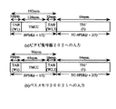
図76は送信側の誤り訂正符号化装置10001の構成例を示すブロック図である。本図に示す誤り訂正符号化装置10001は、TS多重回路10002と、RS(Reed-Solomon)符号化回路10003と、ランダマイズ回路10004と、インターリーブ回路10005と、バイト/シンボル変換回路10006と、たたみ込み符号化器10007と、マッピング回路10008と、伝送制御情報生成回路10009とを有している。
【0007】
このような構成の誤り訂正符号化装置10001の動作について説明する。複数種類のMPEGトランスポート・ストリーム( TS:Transport Stream) が誤り訂正符号化装置10001に入力されると、TS多重回路10002は複数種類のTSを多重し、図77(a)のように多重化TSを生成する(この図の場合は、2種類のTSを想定している)。
【0008】
このような複数TS多重方式は各放送事業者の物理的独立性を持たせるために、各事業者毎にTSを割り当て、フレーム内で多重する方式である。つまり、CSデジタル放送では1トランスポンダで1TSであったが、BSデジタル放送では1トランスポンダで複数のTS(最大で8)を含ませることができる特徴がある。
【0009】
図76のRS符号化回路10003は、図77(a)に示すデータ系列に対して、RS(204、188)の符号化を行い、MPEGのTS188バイトに対して、16バイトのパリティを付加して、図77(b)のようなデータ系列で出力する。48MPEGパケットを1フレームとし、8フレームを1スーパーフレームとする。ランダマイズ回路10004は、図77(b)のデータ系列に対して、1スーパーフレーム(48MPEGパケット×8フレーム)の周期でランダマイズを行い、インターリーブ回路10005に出力する。図77(c)に示すように、ランダマイズ回路10004内のPN発生器は、各スーパーフレームの第1フレームの2バイト目でリセットされ、生成多項式を用いて入力データの乗算を行う。但し、各MPEGパケット204バイトの先頭バイト(MPEG同期バイト:47h)の期間はPN発生器はフリーランとして、データへの乗算は行わない。
【0010】
なお、ランダマイズの際のPN(Pseudo-random Noise )系列は、
生成多項式を1 +x14 +x15 とし、初期値を(100101010000000 )とする。
【0011】
図77(d)は伝送フレームの構造図である。ランダマイズ後の204バイトが1スロットであり、1フレームは48スロット、1スーパーフレームは8フレームで構成される。各スロットの先頭バイトは、インターリーブ後にスーパーフレームの各種情報を含む伝送制御情報に置き換えられる。
【0012】
ランダマイズされたデータ系列は、インターリーブ回路10005においてインターリーブされ、バイト/シンボル変換回路10006に出力される。インターリーブは、各スロットの先頭バイトを除いた203バイトについて、スロット単位で深さ8のブロック・インターリーブが48スロット分行われる。即ち図78に示すように、8×203バイトのインターリーブとする。そしてスロット毎にスーパーフレーム方向で深さ8のブロックインターリーブを行う。次に第1〜8フレームのi番目のスロットをまとめてインターリーブを行い、1/8毎にi番目のスロットに戻す(1≦i≦48)。
【0013】
以上のようなインターリーブが行われるが、ここで、第iスロットについての実際の読み出しアドレス値を示すと(数字は、フレーム−バイトを示す)、次のようになる。

以上のように、インターリーブ回路10005では、スロット単位で深さ8のブロック・インターリーブが48スロット分行われる。符号化率をrとすると、上述したようにスーパーフレーム内には階層化伝送のために、TC−8PSK(r=2/3)、QPSK(r=3/4、1/2)、BPSK(r=1/2)のデータが存在する。1フレームは48スロットで構成され、1スーパーフレームは48×8スロットで構成されるが、全スロットをTC−8PSK(r=2/3)で伝送した場合には48スロット分のデータを丸々送信可能である。一方、QPSK(r=3/4)、QPSK(r=1/2)、BPSK(r=1/2)は、TC−8PSK(r=2/3)と比べて、伝送効率がそれぞれ3/4、1/2、1/4に減少する。
【0015】
1スーパーフレームの伝送時間は一定なので、図79(a)に示すように、QPSK(r=1/2)のスロットを伝送する場合、2スロット当たり1スロットがダミー・スロットとしてインターリーブ回路10005に入力されることになるが、出力時には2スロット当たり1スロットの有効スロットのみが入力時の1/2の速度で読み出される。同様にして、図79(b),(c)に示すように、QPSK(r=3/4)は4スロット当たり1スロット、BPSK(r=1/2)は4スロット当たり3スロットがそれぞれダミー・スロットとなる。
【0016】
前述のように、各スロットの先頭バイト(MPEG同期バイト:47h)はインターリーブ後に、スーパーフレームの各種情報を含む伝送制御情報(TMCC:Transmission Multiplexing Configuration Control )に置き換えられる。図80は伝送制御情報生成回路10009の構成例である。本図に示すように、伝送制御情報生成回路10009は、制御情報発生部10010と、RS符号化回路10011と、TAB信号挿入部10012と、ランダマイズ回路10013とを有している。
【0017】
TMCCは、48スロット×8フレーム=384スロット内の各スロットの先頭バイトを1スーパーフレーム分集めた384バイトを置き換えて、スーパーフレーム単位で生成される。TMCCは重要な情報であるため、各フレームの先頭で主信号に先立ち、BPSK(r=1/2)で伝送が行われる。従って、伝送効率がTC−8PSK(r=2/3)の1/4であるため、実際に伝送されるデータは96バイト(=384バイト/4)である。
【0018】
伝送制御情報生成回路10009の動作を以下に説明する。図80において、制御情報発生部10010は、2つ後のスーパーフレームの伝送制御情報としてTMCC48バイトを発生し、RS符号化回路10011に出力する。また制御情報発生部10010は変調パラメータを図76のバイト/シンボル変換回路10006、たたみ込み符号化器10007、及びマッピング回路10008に出力する。
【0019】
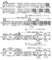
図81にTMCC48バイト(384ビット)の内容の一例を示す。BSデジタル放送では、1変調波内に複数TSの採用及び放送事業者による複数変調方式の運用切替を可能とするため、48スロットからなる伝送フレーム構成、即ち1スーパーフレーム=8フレームとなっている。これらはMPEG2Systemの制御情報に対して、放送用として新たに付加された制御情報である。各スロットの伝送モードやTSとの関係を明確化するための情報として、このような伝送制御情報(TMCC)を伝送する必要がある。さらに、TMCCは変復調に関係する情報を伝送するための信号でもあるため、送受信制御に関する情報をここに含ませる。図81において、バージョン情報はTMCCの内容変更を指示するもので、例えば内容を変更するたびに1ずつインクリメントされる。受信機では、この情報を監視することにより、TMCCの内容変更のタイミングを認識することができる。
【0020】
図82に伝送モード/スロット情報の構成の一例を示す。伝送モードは、使用する変調方式と内符号(たたみ込み符号)との組み合わせを示す項目である。図中で割り当てスロット数は、直前の伝送モードに割り当てられる1フレームあたりのスロット数を示す(前述のダミー・スロット分を含む)。なお、使用されない伝送モードは、直後の割り当てスロット数が0であることで識別される。主信号内においては、図82に示すように、位相数の多い変調方式、符号化率の高い内符号方式の伝送モード順にスロットへ配置される。
【0021】
図83に相対TS/スロット情報の構成の一例を示す。1変調波内で複数TSを伝送するため、各TSが伝送フレーム内のどのスロットに配置されているかを明示する必要がある。MPEG2Systemで使用されているTS_IDは16ビットであるため、そのまま使用するのは伝送効率上好ましくない。その代わりに、3ビットの相対TS/スロット情報により、各スロットで伝送されるTSを相対TS番号を使用して、スロット1から順に各スロット毎に示すものとする。相対TS番号を3ビットとすることにより、1変調波内で最大8TSの伝送が可能である。
【0022】
図84に相対TS/TS対応表の構成の一例を示す。各相対TS番号に対するTS_ID(16ビット)の対応表を持つことにより、相対TS番号の使用は変復調部のみで完結する。
【0023】
図85、図86にそれぞれ、送受信制御情報、拡張情報の構成の一例を示す。送受信制御情報では、緊急警報放送における受信機起動制御のための信号や、アップリンク局切替のための制御信号を伝送する。また、拡張情報は将来のTMCC拡張のために使用するフィールドである。
【0024】
以上に示すTMCC48バイトが図80の制御情報発生部10010から出力されると、RS符号化回路10011はRS(64、48)の符号化を行い、TMCC48バイトに対して16バイトのパリティを付加して出力する。TAB信号挿入部10012は、図87に示すように、RS符号化された64バイトのデータ系列をそれぞれ8フレーム分に分割し、分割した8バイトの前と後に2バイトずつのTAB信号を挿入して、1スーパーフレームあたり96バイト(1フレームあたり12バイト)のTMCCをランダマイズ回路10013に出力する。ここで、TAB信号の内、W1(= 1B95h)はフレーム同期用、W2(= A340h)はスーパーフレーム識別用である。TAB信号について以降の説明では、たたみ込み符号化前の信号を大文字Wで表記し、たたみ込み符号化後の信号を小文字wで表記する。
【0025】
図80のランダマイズ回路10013は、TAB信号挿入部10012から出力されたデータ系列に対して、TMCC1スーパーフレーム分(96バイト)の周期でランダマイズを行い、図76のバイト/シンボル変換回路10006に出力する。ランダマイズ回路10004のPN発生器は、図88に示すように各スーパーフレームの第1フレームの3バイト目でリセットされ、入力データと乗算が行われる。但し、各TAB信号(W1、W2、W3)の期間フリーランとして、データへの乗算は行われない。
【0026】
以上のように、伝送制御情報生成回路10009は、1スーパーフレームあたり96バイトのTMCCをバイト/シンボル変換回路10006に出力するとともに、スーパーフレーム内のデータ系列の変調パラメータ(位相数、符号化率)を図76のバイト/シンボル変換回路10006、たたみ込み符号化器10007、及びマッピング回路10008に出力する。
【0027】
伝送制御情報生成回路10009から出力される1フレームあたり12バイトのTMCCと、インターリーブ回路10005から出力される1フレームあたりTC−8PSK換算で203×48バイトの主信号は、図87に示すスーパーフレーム構造でバイト/シンボル変換回路10006に入力される。即ち、各フレームの先頭12バイトがTMCCであり、続く203×48バイトが主信号であり、8フレーム集まって1スーパーフレームの構造を取る。なお、図89に示すように、主信号は各フレームにおいて、変調多値数(位相数)の大きいものから順に並んでいる。但し、QPSKについては符号化率r=3/4→r=1/2のように符号化率の高い方から並んでいる。
【0028】
バイト/シンボル変換回路10006は、伝送制御情報生成回路10009から出力される変調パラメータに従って、入力されるスーパーフレーム構造のバイトデータ系列を、図90に示すように、各位相数・符号化率に対応するシンボルデータ系列に変換する。なお、図90に示すシンボル出力はTC−8PSK(r=2/3)が並列2ビット、QPSK(r=3/4、1/2)、BPSK(r=1/2)が1ビットである。
【0029】
バイト/シンボル変換回路10006から出力されるスーパーフレーム構造のシンボルデータ系列は、たたみ込み符号化器10007に入力される。図91はたたみ込み符号化器10007の構成例を示すブロック図である。このたたみ込み符号化器10007は、点線部で示すたたみ込み回路10014と、パンクチャド・P/S(Parallel to Serial)回路10015とからなる。
【0030】
たたみ込み回路10014にシンボルデータ系列D[2:1] が入力されると、たたみ込み回路10014がLSBのD[1] =D1を拘束長7、符号化率1/2でたたみ込み符号化を行って、2ビットのシンボルC1,C0をパンクチャド・P/S回路10015に出力する。また、シンボルデータ系列のMSBのD[2] =D2についてはたたみ込み符号化せずに、符号化シンボル(C2、C1、C0)のMSBであるC2をパンクチャド・P/S回路10015に出力する。
【0031】
パンクチャド・P/S回路10015は、伝送制御情報生成回路10009から出力される変調パラメータに従って、図92〜図95に示すようにパンクチャド処理とP/S変換とを行い、各位相数・符号化率に対応する符号化シンボルデータをマッピング回路10008に出力する。但し、TC−8PSK(r=2/3)とQPSK(r=1/2)では何も処理しない。このように異なる変調方式(位相数)及び符号化率を越えて、1つのたたみ込み回路10014で連続的にシンボルデータ系列のたたみ込み符号化が行われる。
【0032】
図92はTC−8PSK(r=2/3)の場合の動作例を示す。この場合、たたみ込み符号化器10007に入力されたシンボルデータD[2:1] は、LSBのD[1] がたたみ込み回路10014でたたみ込み符号化が行われて2ビットの符号化シンボルC1,C0となる。またMSBのD[2] はたたみ込み符号化されずに符号化シンボルのMSBのC2となる。これらのシンボルC0〜C2はパンクチャド・P/S回路10015に出力される。パンクチャド・P/S回路10015は、何の処理もせずに1シンボル=3ビットの8PSKシンボルデータC2、C1、C0をマッピング回路10008に出力する。この場合、たたみ込み符号化器10007に入力された1シンボル(2ビット)が符号化され、1シンボル(3ビット)が出力される。従って、たたみ込み符号化器10007全体として、符号化率はr=2/3となる。
【0033】
図93はQPSK(r=3/4)の場合の動作例を示す。たたみ込み符号化器10007に入力されたシンボルデータD[2:1] (但し、MSBのD[2] は無効)は、LSBのD[1] がたたみ込み回路10014でたたみ込み符号化が行われてC1,C0の2ビットになり、パンクチャド・P/S回路10015に出力される。パンクチャド・P/S回路10015では図93に示すように、3シンボル=6ビットのデータより規則的に2ビットを廃棄処理、即ちパンクチャド処理し、残りの4ビットのデータより1シンボル=2ビットのQPSKシンボルデータC1,C0を生成し、マッピング回路10008に出力する。なおMSBのシンボルC2は無効する。この場合、たたみ込み符号化器10007に入力された3シンボル(3ビット)が符号化され、2シンボル(4ビット)が出力される。従って、たたみ込み符号化器10007全体として、符号化率はr=3/4となる。
【0034】
図94はQPSK(r=1/2)の場合の動作例を示す。たたみ込み符号化器10007に入力されたシンボルデータD[2:1] (但し、MSBのD[2] は無効)は、LSBのD[1] がたたみ込み回路10014でたたみ込み符号化が行われてC1 ,C0の2ビットになり、パンクチャド・P/S回路10015に出力される。パンクチャド・P/S回路10015は何の処理もせずに、1シンボル=2ビットのQPSKシンボルデータC1,C0をマッピング回路10008に出力する。但しMSBのシンボルC2を無効とする。この場合、たたみ込み符号化器10007に入力された1シンボル(1ビット)が符号化され、1シンボル(2ビット)が出力される。従って、たたみ込み符号化器10007全体として、符号化率はr=1/2となる。
【0035】
図95はBPSK(r=1/2)の場合の動作例を示す。たたみ込み符号化器10007に入力されたシンボルデータD[2:1] (但し、MSBのD[2] は無効)は、LSBのD[1] がたたみ込み回路10014でたたみ込み符号化が行われてC1,C0の2ビットになり、パンクチャド・P/S回路10015に出力される。パンクチャド・P/S回路10015は図95に示すように、各シンボルC1,C0の2ビットのP/S変換を行い、C0→C1の順に1シンボル=1ビットのBPSKシンボルデータ(C0/C1)をマッピング回路10008に出力する。但しMSBより2ビットは無効とする。この場合、たたみ込み符号化器10007に入力された1シンボル(1ビット)が符号化され、2シンボル(2ビット)が出力される。従って、たたみ込み符号化器10007全体として、符号化率はr=1/2となる。
【0036】
図92〜図95に示すように、たたみ込み符号化器10007から出力されるシンボルデータは、一定のシンボル速度で図76のマッピング回路10008に出力される。マッピング回路10008は、伝送制御情報生成回路10009から出力される変調パラメータに従って、図96に示すようにBPSK、QPSK、TC−8PSKのマッピングを夫々行い、マッピングされたI(In-Phase)軸、Q(Quadrature Phase)軸のデータを、図示しない直交変調器に出力する。
【0037】
以上に説明した誤り訂正符号化装置10001の入力から出力までの信号の流れを1フレームあたりでまとめると、図97のようになる。ここではTS1とTS2の2種類のTSを1つの変調波で伝送するものとし、1フレーム(48スロット)あたり、
【0038】
図97(a)に示すようなTS1とTS2が図76の誤り訂正符号化装置10001に入力されると、TS多重回路10002は2つのTSを多重化する。そしてRS符号化回路10003がRS(204,188)符号化を行う。そしてランダマイズ回路10004がランダマイズを行い、図97(b)に示すように1フレームあたり48スロット(1スロット=204バイト)のデータ系列を出力する。但し、48スロットの内、斜線の4スロットはダミー・スロットである。ここで、データ系列は変調多値数(位相数)の大きいものから順に並べ、QPSKについては符号化率r=3/4→r=1/2のように符号化率の高い方から並べる。
【0039】
インターリーブ回路10005は、各スロットの内の先頭バイト(MPEG同期バイト:47h)を除いた203バイトについて、前述のようにスロット毎にスーパーフレーム方向に、深さ8のブロック・インターリーブを行う。また、伝送制御情報生成回路10009はTMCCを生成し、各スロットの先頭バイトであるMPEG同期バイト:47hと置き換える。その結果、図97(c)に示すように、バイト/シンボル変換回路10006には、各フレームについてTAB信号を含むTMCC12バイトに続き、203バイト×44スロットの主信号で構成されたバイトデータ系列が入力される。
【0040】
バイト/シンボル変換回路10006は、入力されたバイトデータ系列を、各スロットの伝送モード(位相数・符号化率)に対応したシンボルデータ系列に変換する。たたみ込み符号化器10007は、各スロットの伝送モードに対応したたたみ込み符号化を行う。またマッピング回路10008は各スロットの位相数に応じたマッピングを行い、図97(d)に示すデータ系列を図示しない直交変調器に出力する。なお、図97(d)に示すように、TMCC12バイト、即ち1フレームあたり96ビットは、BPSK(r=1/2)の符号化が行われるため、192シンボル(1シンボル=1ビット)となる。
【0041】
また主信号において、TC−8PSKの1スロット(203バイト)、即ち1624ビットは、符号化の結果812シンボル(1シンボル=3ビット)となる。QPSK(r=1/2)の1スロット(203バイト:ダミーを含めると2スロット分)、即ち1624ビットは、符号化の結果1624シンボル(1シンボル=2ビット)となる。BPSK(r=1/2)の1スロット(203バイト:ダミーを含めると4スロット分)、即ち1624ビットは符号化の結果3248シンボル(1シンボル=1ビット)となる。以上より、1フレームはTMCC192シンボルと、主信号38976シンボル(812×48)とより構成される。
【0042】
次に、以上に示した誤り訂正符号化装置10001で誤り訂正符号化されたデータ系列を誤り訂正復号する回路を、これまでに検討されてきた誤り訂正回路(以下、従来例の誤り訂正回路という)、として図面を参照しながら以下に説明する。
【0043】
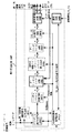
図98は従来例の誤り訂正回路20001の構成例を示すブロック図である。この誤り訂正回路20001は、ビタビ復号器20002と、高/低階層選択信号生成回路20003と、シンボル/バイト変換回路20004と、デ・インターリーブ回路20005と、MPEG同期バイト/ダミー・スロット挿入回路20006と、デ・ランダマイズ回路20007と、RS復号回路20008と、速度変換回路20009と、伝送制御情報復号回路20010と、選局回路20011とを有している。
【0044】
このような構成の誤り訂正回路20001の動作について以下に説明する。図76の誤り訂正符号化装置10001で誤り訂正符号化されたデータ系列が、図示しない直交変調器によって直交変調され、トランポンダを含む衛星伝送路を通して送信される。この信号は図示しない受信側のPSK復調器でPSK復調される。図91で説明したたみ込み回路10014の拘束長は7であり、TAB信号区間はBPSKで伝送される。このためビタビ復号前のTAB信号(w1、w2、w3)は、図87に示すようにそれぞれ32シンボル(16×2=32ビット)の内、先頭12シンボル(6ビット×2)は不確定である。しかし、残りの32−12=20シンボルはw1(=xxxECD28h )、w2(=xxx0B677h )、w3(=xxxF4988h )のうちいずれかと確定する。PSK復調器は、選局情報により選局が切り替えられると、まず遅延検波により復調を行い、w1、w2、w3を検出することにより、スーパーフレーム同期と絶対位相とを検出する。検出後は同期検波を行ってPSK復調データ及びスーパーフレーム同期信号を誤り訂正回路20001に出力する。
【0045】
誤り訂正回路20001内の伝送制御情報復号回路20010は、PSK復調器より出力されたスーパーフレーム同期信号により、各フレームのTMCC192シンボル区間について制御信号(伝送モード)を生成し、ビタビ復号器20002に出力する。ビタビ復号器20002は、図97(d)に示す各フレームのTMCC192シンボル区間について、制御信号に従いBPSK(r=1/2)のビタビ復号を行う。そして192シンボル×1/2=96シンボル(96ビット)のビタビ復号データを伝送制御情報復号回路20010に出力する。なお、ビタビ復号器20002の詳細については後述する。
【0046】
伝送制御情報復号回路20010の構成例を図99に示す。この伝送制御情報復号回路20010は、デ・ランダマイズ回路20012と、シンボル/バイト変換回路20013と、RS復号回路20014と、TMCC解読回路20015とを有している。
【0047】
伝送制御情報復号回路20010では、デ・ランダマイズ回路20012がビタビ復号器20002より出力される1フレームあたり96シンボル(96ビット)、即ち1スーパーフレームあたり768ビット(96バイト)のTMCCを、図88に示すようにTMCC1スーパーフレーム分(96バイト)の周期でデ・ランダマイズを行い、シンボル/バイト変換回路20013に出力する。図88に示すように、デ・ランダマイズ回路20012内のPN発生器は、図76のランダマイズ回路10004と同様に、各スーパーフレーム分の第1フレームの3バイト目でリセットされ、入力データと乗算が行われる。但し、各TAB信号(W1、W2、W3)の期間はPN発生器はフリーランとして、データへの乗算は行われない。
【0048】
図99のシンボル/バイト変換回路20013は、入力された1スーパーフレームあたり768シンボル(768ビット)のデータ系列を96バイトのバイトデータ系列に変換してRS復号回路20014に出力する。図87に示すように、各フレームの12バイト中、TAB信号(W1とW2又はW3)が前後に2バイトずつ含まれるので、正味のTMCC信号は1フレームあたり8バイト(1スーパーフレームあたり64バイト)である。図99のRS復号回路20014は、正味のTMCC信号64バイトに対して、RS(64、48)の復号を行い、48バイトの訂正済みTMCCをTMCC解読回路20015に出力する。
【0049】
TMCC解読回路20015は、48バイトの訂正済みTMCCの内容を図81〜図86に示す信号配置図と照合して解読し、伝送モード、ダミー・スロット情報などの各種伝送制御情報を出力し、MPEGのTS_IDと相対TS番号との参照などを行う。前述のように、伝送制御情報復号回路20010において解読を行ったTMCCは、2つ後のスーパーフレームに適用される各種伝送制御情報である。図87に示すように、TMCCはスーパーフレーム内の1〜8フレーム目の先頭に配置されている。伝送制御情報復号回路20010に8フレーム目のTMCC(パリティ2)が入力されるまでは、TMCCの解読は完了されない。しかしながら、8フレーム目の主信号は図87に示すようにTC−8PSK換算で203×48バイト、シンボルで換算すると図97(d)に示すように812×48シンボルあり、更に1スーパーフレーム分の時間余裕があるので、この期間でTMCCの解読は十分に完了可能である。
【0050】
さて、PSK復調器より出力されたスーパーフレーム構造のシンボルデータ系列(I/Q軸)がビタビ復号器20002に入力されると、ビタビ復号器20002はビタビ復号を行い、復号データを高/低階層選択信号生成回路20003と、シンボル/バイト変換回路20004に出力する。
【0051】
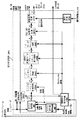
図100はビタビ復号器20002と高/低階層選択信号生成回路20003の構成例を示すブロック図である。下側破線部で示すビタビ復号器20002は、デ・パンクチャド・S/P(Serial to Parallel)回路20016と、点線部で示すビタビ復号化回路20017とを有している。ビタビ復号化回路20017はブランチメトリック計算回路20018と、ACS(Add 、 Compare、 Select )回路20019と、パスメトリックメモリ20020と、パスメモリ20021とを有している。また上側破線部で示す高/低階層選択信号生成回路20003は、8PSK硬判定回路20022と、M段遅延回路20023と、BER(Bit Error Rate)測定回路20024と、たたみ込み回路20025とを有している。
【0052】
ビタビ復号器20002にPSK復調シンボルデータ系列(I/Q軸)が入力されると、デ・パンクチャド・S/P回路20016は、伝送制御情報復号回路20010から出力される伝送モードに従って、図101〜図104に示すように、各スロットの伝送モードに対応したデ・パンクチャド処理、及びS/P変換を行い、ビタビ復号化回路20017に出力する。デ・パンクチャド処理及びS/P変換されたデータは、図98の伝送制御情報復号回路20010から出力される伝送モードに従って、ビタビ復号化回路20017において各スロットの伝送モードに対応したビタビ復号が行われる。そしてビタビ復号シンボルはシンボル/バイト変換回路20004に出力される。誤り訂正符号化装置10001におけるたたみ込み符号化は、図91に示すように1つのたたみ込み回路10014で連続的に行われるので、図98の誤り訂正回路20001におけるビタビ復号は、1つのビタビ復号器20002で連続的に復号可能である。
【0053】
図101はTC−8PSK(r=2/3)の場合の復号動作例を示す説明図である。ビタビ復号器20002に入力された8PSK復調シンボルデータ(I/Q軸)は、デ・パンクチャド・S/P回路20016では何の処理もされず、ビタビ復号化回路20017にそのまま出力される。ビタビ復号化回路20017では、ブランチメトリック計算回路20018が、図96に示す8PSKの8つの符号点とのブランチメトリック、例えばユークリッド距離を計算する。ここで計算されたブランチメトリックを基に、ACS回路20019、パスメトリックメモリ20020、及びパスメモリ20021によってビタビ復号が行われる。そして1シンボル=2ビットのビタビ復号シンボル(図92のD[2:1] に対応)が、図98のシンボル/バイト変換回路20004に出力される。
【0054】
図102はQPSK(r=3/4)の場合の復号動作例を示す説明図である。ビタビ復号器20002に入力されたQPSK復調シンボルデータ(I/Q軸)が、デ・パンクチャド・S/P回路20016に入力されると、図91のパンクチャド・P/S回路10015でパンクチャド処理されて廃棄されたシンボルについて、デ・パンクチャド・S/P回路20016がヌル・シンボルを挿入し、2シンボルを3シンボルに変換する。なお、ヌル・シンボルとは、Q軸上で得られた2種類の符号点の中間値、又はI軸上で得られた2種類の符号点の中間値とする。これらのシンボルは図100のビタビ復号化回路20017に出力される。ビタビ復号化回路20017では、ブランチメトリック計算回路20018が、図96に示すQPSKの4つの符号点とのブランチメトリックを計算する。そして計算されたブランチメトリックを基に、ACS回路20019、パスメトリックメモリ20020、及びパスメモリ20021によってビタビ復号が行われる。こうして1シンボル=1ビットのビタビ復号シンボル(図93のD[1] に対応:MSBのD[2] は無効)が図98のシンボル/バイト変換回路20004に出力される。
【0055】
図103はQPSK(r=1/2)の場合の復号動作例を示す説明図である。ビタビ復号器20002に入力されたQPSK復調シンボルデータ(I/Q軸)は、デ・パンクチャド・S/P回路20016では何の処理もされずにビタビ復号化回路20017にそのまま出力される。ビタビ復号化回路20017では、ブランチメトリック計算回路20018が、図96に示すQPSKの4つの符号点とのブランチメトリックを計算する。そして計算されたブランチメトリックを基に、ACS回路20019、パスメトリックメモリ20020、及びパスメモリ20021によってビタビ復号が行われる。こうして1シンボル=1ビットのビタビ復号シンボル(図94のD[1] に対応し、MSBのD[2] は無効とする)が、図98のシンボル/バイト変換回路20004に出力される。
【0056】
図104はBPSK(r=1/2)の場合を復号動作例を示す説明図である。ビタビ復号器20002に入力されたBPSK復調シンボルデータのI軸(Q軸データは無効)は、デ・パンクチャド・S/P回路20016において、入力2シンボル毎に(I、Q)の1シンボルにS/P変換が行われてビタビ復号化回路20017に出力される。ビタビ復号化回路20017では、ブランチメトリック計算回路20018が、図96に示すQPSKの4つの符号点とのブランチメトリックを計算する。そして計算されたブランチメトリックを基に、ACS回路20019、パスメトリックメモリ20020、及びパスメモリ20021によってビタビ復号が行われる。こうして1シンボル=1ビットのビタビ復号シンボル(図95のD[1] に対応し、MSBのD[2] は無効とする)が、シンボル/バイト変換回路20004に出力される。
【0057】
図105はTC−8PSK(r=2/3)の場合のビタビ復号化回路20017の動作を示すトレリス線図である。図91に示すように、誤り訂正符号化装置10001のたたみ符号化器10007においては、MSBのD[2] (=D2)は符号化されていない。従ってD[2:1] =(D2,D1)として(0,0)及び(1,0)、D[2:1] として(0,1)及び(1,1)は、図105のトレリス線図において同じ状態と見なされる。従って、時刻tにおいてある1状態から出力され、時刻(t+1)において同じ状態に入力するブランチは2つ存在する。従って図105に示すように、時刻(t+1)において、状態Sに入力されるブランチは4つあり、ビタビ復号化回路20017はその中から最小のパスメトリックを有するブランチを図105の太線のように生き残りパスとする。各ブランチに対応する復号シンボルは2ビットであり、パスメモリ20021より最尤パスのブランチに対応する2ビットの復号シンボルが図98のシンボル/バイト変換回路20004に出力される。
【0058】
一方、図106はQPSK(r=3/4、1/2)及びBPSK(r=1/2)の場合のビタビ復号化回路20017の動作を示すトレリス線図である。図91に示すように、誤り訂正符号化装置10001のたたみ符号化器10007においては、MSBのD[2] は無効である。従って、時刻tにおいてある1状態から出力され、時刻(t+1)において同じ状態に入力するブランチは1つである。図106に示すように、時刻(t+1)において、状態Sに入力されるブランチは2つあり、ビタビ復号化回路20017はその中から最小のパスメトリックを有するブランチを例えば図106の太線のように生き残りパスとする。各ブランチに対応する復号シンボルは1ビットであり、パスメモリ20021より最尤パスのブランチに対応する1ビットの復号シンボルがシンボル/バイト変換回路20004に出力される。
【0059】
なお図91に示すように、たたみ込み回路10014には6つのレジスタが設けられている。従って図105及び図106のトレリス線図における状態数はどちらも64である。即ち状態“000000”〜状態“111111”のいずれかである。
【0060】
一方、PSK復調シンボルデータ系列が高/低階層選択信号生成回路20003に入力されると、図100に示すように、8PSK硬判定回路20022は伝送制御情報復号回路20010から出力される伝送モードに従って、TC−8PSK(r=2/3)のスロットのみを、図96に示すTC−8PSKの符号点に硬判定し、1シンボル=3ビットの硬判定結果を出力する。M段遅延回路20023はビタビ復号器20002の処理遅延分(M段)遅延させてタイミングを合わせてBER測定回路20024に出力する。また、ビタビ復号器20002から出力されたTC−8PSKのスロットのビタビ復号データの各シンボル(1シンボル=2ビット)がたたみ込み回路20025に入力される。このたたみ込み回路20025は図91のたたみ込み回路10014と同じ構成である。ここで再たたみ込み符号化された各シンボル(1シンボル=3ビット)のデータは、BER測定回路20024に出力される。
【0061】
BER測定回路20024はTC−8PSKのスロットの各シンボル(1シンボル=3ビット)を比較してBERを測定し、その結果により高/低階層選択信号(‘H’=高階層、‘L’=低階層)を生成して、誤り訂正回路20001に続くMPEG復号器(図示せず)に出力する。BERが低い場合には、‘H’信号を出力し、BERが高い場合には‘L’信号を出力する。MPEG復号器は‘H’信号が入力されると高階層信号をMPEG復号して画像をモニタに出力し、‘L’信号が入力されると低階層信号をMPEG復号して画像をモニタに出力する。
【0062】
図98のシンボル/バイト変換回路20004は、伝送制御情報復号回路20010から出力される伝送モードに従って、入力されるビタビ復号シンボルデータ系列を、各スロットの伝送モードに対応してバイトデータ系列に変換する。この状態を図107に示す。TC−8PSK(r=2/3)では、4シンボル(1シンボル=2ビット)を集めてバイトデータに変換する。QPSK(r=3/4、1/2)及びBPSK(r=1/2)では、8シンボル(1シンボル=1ビット)を集めてバイトデータに変換する。そしてこれらの変換データをデ・インターリーブ回路20005に出力する。
【0063】
ここで、誤り訂正符号化装置10001から出力される1フレームあたりのデータ系列を、図97で示したように、
【0064】
デ・インターリーブ回路20005ではデ・インターリーブが施され、ここでデ・インターリーブされたデータは、MPEG同期バイト/ダミー・スロット挿入回路20006に出力される。このデ・インターリーブ処理では、TMCC部分(TC−8PSK換算で48バイト分)を除いた各スロット203バイトについて、スロット単位で深さ8のブロック・デ・インターリーブが48スロット分行われる。但し、ダミー・スロット分については行われない。図109に示すように、8×203のデ・インターリーブとすると、スロット毎にスーパーフレーム方向で深さ8のブロック・デ・インターリーブを行う。こうして第1〜8フレームのi番目のスロットをまとめてデ・インターリーブを行い、1/8毎にi番目のスロットに戻す(1≦i≦48)。以上のようなデ・インターリーブ処理は、送信側のインターリーブ回路10005と書き込み/読み出し方向が逆である。
【0065】
図110はデ・インターリーブ回路20005の構成例である。このデ・インターリーブ回路20005は、書き込みアドレス生成回路20026と、読み出しアドレス生成回路20027と、メモリ回路20028とを有している。なお、デ・インターリーブを行うために、メモリ回路20028は1スーパーフレーム(48×8スロット)の2バンク分のメモリ領域を使用する。ここで第iスロットについての実際の書き込みアドレス値を示すと、以下のようになる。なお、数字はフレーム−バイトを示す。
以上のように、デ・インターリーブ回路20005では、スロット単位で深さ8のブロック・デ・インターリーブが48スロット分行われる。ただし、図108(c)に示すように、各フレームのTMCC区間がMPEG同期48バイト(48スロット分)期間に利用される。従ってデ・インターリーブ回路20005は、各スロットの先頭にMPEG同期1バイト分の隙間を空けて各スロットを出力する。さらにデ・インターリーブ回路20005は、ダミー・スロット分の隙間も空けて図108(c)に示すように1フレームあたり48スロット(ダミー・スロットを含む)を一定の速度で出力する。
【0067】
図110に示すデ・インターリーブ回路20005の動作は以下の通りである。図109に示すように、各スロットについて書き込みアドレス生成回路20026、読み出しアドレス生成回路20027が、それぞれ書き込みアドレス、読み出しアドレスを生成し、メモリ回路20028に出力する。図108(b)に示すように、シンボル/バイト変換回路20004から出力されたバイトデータ系列は、書き込みアドレス及び読み出しアドレスに従って、メモリ回路20028に読み書きされて、図108(c)のようにデ・インターリーブされたバイトデータ系列が、図98のMPEG同期バイト/ダミー・スロット挿入回路20006に出力される。ただし、伝送制御情報復号回路20010から出力されたダミー・スロット情報に従って、書き込みアドレス生成回路20026及び読み出しアドレス生成回路20027は、ダミー・スロット分のアドレスを飛ばして、有効スロット分のアドレスを順に生成する。
【0068】
MPEG同期バイト/ダミー・スロット挿入回路20006は、各スロットの先頭にMPEG同期バイトを挿入する。かつ、伝送制御情報復号回路20010から出力されたダミー・スロット情報に従って、ダミー・スロット区間にMPEGヌル・パケットを挿入して、図108(d)に示すようなバイトデータ系列をデ・ランダマイズ回路20007に出力する。
【0069】
図111にデ・ランダマイズ回路20007の構成例を示す。デ・ランダマイズ回路20007は、破線部で示すPN発生回路20029と、P/S変換回路20030と、S/P変換回路20031と、ゲート信号生成回路20032と、ex−or(exclusive-or)回路20033とを有している。デ・ランダマイズ回路20007は、送信側のランダマイズ回路10004と同様に、図108(d)のデータ系列に対して1スーパーフレームの周期でデ・ランダマイズを行う。図111に示すように、PN発生回路20029は生成多項式(1 +x14 +x15 )を用いて信号処理を行うもので、各スーパーフレームの第1フレームの2バイト目でリセットされ、初期値“100101010000000 ”が代入される。そしてP/S変換回路20030でビット系列に変換された入力データとの乗算がex−or回路20033で行われる。乗算結果はS/P変換回路20031でバイトデータ系列に変換されて、図98のRS復号回路20008に出力される。但し図112に示すように、ゲート信号生成回路20032が生成するゲート信号により、各スロット204バイトの先頭バイト、及びダミー・スロットの期間はPN発生回路20029はフリーランとしてデータへの乗算は行われない。
【0070】
RS復号回路20008は、デ・ランダマイズ回路20007より出力された204バイトのスロット毎にRS(204、188)の復号を行って、速度変換回路20009に出力する。ただし、RS復号回路20008は伝送制御情報復号回路20010より出力されるダミー・スロット情報により、ダミー・スロットに対しては復号を行わない。
【0071】
速度変換回路20009は、RS復号回路20008より出力される1フレームあたり48スロットのデータ系列より、選局された1つのTSを選択し、図108(e)に示すように速度変換を行って、誤り訂正データ系列(TS)を図示しないMPEG復号器に出力する。
【0072】
図113に速度変換回路20009の構成例を示す。点線部で示す速度変換回路20009は、書き込みアドレス生成回路20034と、読み出しアドレス生成回路20035と、メモリ回路20036とを有している。なお、TSの選択と速度変換を行うために、メモリ回路20036は1フレーム分(48スロット)のメモリ領域を使用する。また、図113には伝送制御情報復号回路20010と、選局回路20011も図示されている。
【0073】
図示しないMPEG復号器より選局情報(16ビットのTS_ID)が選局回路20011に入力されると、選局回路20011は伝送制御情報復号回路20010に対してTS_IDを出力する。伝送制御情報復号回路20010は、図84に示す相対TS/TS対応表を参照し、該当するTS_IDの相対TS番号を選択する。次いで図83に示す相対TS/スロット情報を参照し、選択された相対TS番号のスロット番号情報を選局回路20011に出力する。選局回路20011はスロット番号情報より、速度変換回路20009に対してTSの選択を行うためのスロット選択信号を出力する。
【0074】
速度変換回路20009においては、書き込みアドレス生成回路20034から出力される書き込みアドレスにより、メモリ回路20036に1フレーム分(48スロット)のデータ系列を順次書き込む。読み出しアドレス生成回路20035は、選局回路20011より出力されたスロット選択信号より、ダミー・スロットを含み、選択されたNスロットのみの読み出しアドレスを生成してメモリ回路20036に出力する。
【0075】
メモリ回路20036より選択されたNスロットのみが速度変換されて、入力のN/48の速度で図示しないMPEG復号器に出力される。図108(e)の場合は、N=24である。読み出しアドレス生成回路20035は、メモリ回路20036より出力される各スロット(204バイト)毎に、MPEGパケット有効期間(188バイト)が‘H’信号で、RS符号のパリティ区間(16バイト)が‘L’信号であるイネーブル信号を図108(e)のように生成し、図示しないMPEG復号器に出力する。このイネーブル信号によりMPEG復号器はMPEGパケット有効期間(188バイト)のみを復号できる。
【0076】
メモリ回路20036より出力される図108(e)の出力系列について、メモリ回路20036への書き込み/読み出しの様子を図114〜図117に示す。メモリ回路20036には、一定の速度で1フレームあたりダミー・スロットを含む48スロットのデータ系列が入力される。図108(e)は、2種類のTSの内TS1(1フレームあたり24スロット)が選択されて、入力の1/2(=24/48)の速度で出力される状態を示している。
【0077】
図114は、フレーム先頭の2スロットTS1(1) 〜 (2) がメモリ回路20036に入力されて書き込まれた時点を示している。その間に1スロットTS1(1) がメモリ回路20036から読み出されて出力される。
【0078】
図115は、図114に続く20スロットTS1(3) 〜 (22) がメモリ回路20036に入力されて書き込まれた時点を示している。その間に10スロットTS1(2) 〜TS1(11) がメモリ回路20036から読み出されて出力される。
【0079】
図116は、図115に続く22スロットTS2(1) 〜 (20) 及びTS1(23)と、ダミー1スロットとがメモリ回路20036に入力され、書き込まれた時点を示している。その間に11スロットTS1(12) 〜TS1(22) がメモリ回路20036から読み出されて出力される。
【0080】
図117は、図116に続く4スロット、即ちTS2(21) 、ダミー3スロットがメモリ回路20036に入力され、書き込まれた時点を示している。その間に2スロット即ちTS1(23) 及びダミー1スロットがメモリ回路20036から読み出されて出力される。
【0081】
以上の図114〜図117に示したように、速度変換回路20009は1フレーム(48スロット:ダミー・スロットを含む)のデータ系列が入力されると、選局されたTSのNスロット、図114〜図117の場合はTS1:N=24を選択して、入力のN/48の速度で図示しないMPEG復号器に出力する。
【0082】
【発明が解決しようとする課題】
従来検討されていた誤り訂正回路20001は、以上のような構成で動作し、誤り訂正データ系列(TS)をMPEG復号器に出力していた。ところで誤り訂正回路20001のビタビ復号器20002においては、スロット間で伝送モード(位相数・符号化率)が変化しても、伝送モードの切替時における制御は考えられていなかった。
【0083】
図118は、伝送モード切替時におけるビタビ復号器20002中のパスメモリ20021(パスメモリ長=J)の様子を示すトレリス線図である。図118(a)は、伝送モードAの最終シンボルまでが図100のパスメモリ20021に入力された時点を示す。図118(b)は、次の伝送モードBの第1シンボルがパスメモリ20021に入力された時点を示す。図118(c)は、伝送モードBの次の(J−2)シンボルまでがパスメモリ20021に入力された時点を示す。
【0084】
従来の誤り訂正回路20001では、パスメモリ20021に入力された最新のシンボル、即ちパスメモリ20021中の第J番目のシンボルの全状態の中で、最小のパスメトリックを有する状態から、その状態に入力している生き残りパスを(J−1)シンボル分前に戻り、該当するパスメモリ20021中の第1番目のシンボルをビタビ復号シンボルデータとして出力していた。
【0085】
しかしながら、図118(b)及び(c)に示すトレリス線図では、モード切替後の伝送モードBの入力シンボルにおける全状態において、最小のパスメトリックを判定し、モード切替前の伝送モードAのビタビ復号データ、即ちモード切替時にパスメモリ20021に残留している(J−1)シンボルについてビタビ復号シンボルデータを出力していることになる。
【0086】
例えば図108(a)に示すように、BPSK(r=1/2)で伝送されるTMCC192シンボルの後に、TC−8PSK(r=2/3)が伝送される場合を考える。この場合、図118において伝送モードAがBPSK(r=1/2)であり、伝送モードBがTC−8PSK(r=2/3)である。従来のビタビ復号方法では、モード切替時にパスメモリ20021に残留している(J−1)シンボルのTMCCシンボルは、符号間距離の小さいTC−8PSK(r=2/3)のシンボル系列における最小パスメトリック判定結果によって復号されることになる。従って、この(J−1)シンボルについてはBPSK(r=1/2)本来の誤り率より悪化してしまうという問題点を有していた。
【0087】
また、従来のビタビ復号方法では、図87に示すようにTMCC192シンボルの前後32シンボルずつの固定系列であるTAB信号(w1、w2、w3)において、後ろ20シンボルが既知であるにも関わらず、PSK復調データ系列をそのままビタビ復号器20002に入力していた。従って、TAB信号の固定系列という特徴を利用していないという問題点も有していた。
【0088】
また、従来の誤り訂正回路20001は、図110に示すようにデ・インターリーブ回路20005において、メモリ回路20028の2スーパーフレーム分、即ち48スロット×8フレーム×2バンクのバイトデータ領域を使用してデ・インターリーブを行っていた。ところがデジタルBS放送においては、1トランスポンダで複数TSを多重して送受信を行い、誤り訂正回路20001は最終的は1つのTSのデータ系列しか出力しない。図108(b)に示すように、デ・インターリーブ回路20005に入力されるデータ系列は1フレーム(48スロット)あたり、
【0089】
さらに、従来の誤り訂正回路20001は、図113に示す速度変換回路20009において、メモリ回路20036の1フレーム分のメモリ領域を使用して、TSの選択と速度変換を行っていた。しかしながら、1TSの1フレーム分、即ち上記の例では最大24スロットのメモリ領域のみでTSの選択と速度変換は可能である。よって、従来の速度変換回路20009は、不必要なメモリ領域を使用して、TSの選択と速度変換を行っているという問題点を有していた。
【0090】
また、デ・インターリーブ回路20005はメモリを元来有しており、上述のように、デ・インターリーブ回路でTSの選択を行うと同時に速度変換を行うと、速度変換回路20009は不要である。よって、このような観点から見ると、従来の誤り訂正回路20001は、不必要な速度変換回路20009を具備しているということがいえる。
【0091】
ところで、この場合にはデ・ランダマイズ回路20007に入力されるデータ系列は連続したスロットではなく、飛び飛びのスロットのデータ系列が入力されることになる。従って、従来のデ・ランダマイズ回路20007を用いた場合には、デ・ランダマイズを行うことができないので、デ・インターリーブ回路20005でTSの選択と速度変換を行うという構成は取れない。従って、従来のデ・ランダマイズ回路20007の構成では、速度変換回路20009を不要にすることができないという問題点を有していた。
【0092】
本発明はこのような従来の問題点に鑑みてなされたものであって、本願の発明では、パスメモリに残留している伝送モード切替前のシンボルについては、切替前の伝送モードの最終シンボルまで累積したパスメトリックにより、最小パスメトリックを判定してビタビ復号データとして出力し、切替後の伝送モードのシンボルの影響を受けないビタビ復号が可能な誤り訂正回路を提供することを目的とする。
【0093】
また本願の発明は、伝送モード切替前の最終シンボルにおける全状態の内、最小のパスメトリックを有する1状態のみを有効とし、他の状態を無効としてビタビ復号データを出力し、切替後の伝送モードのシンボルの影響を受けないビタビ復号が可能な誤り訂正回路を提供することを目的とする。
【0094】
また本願の発明は、伝送モード切替前の最終シンボルにおける全状態の内、最小のパスメトリックを有する1状態のパスメトリックのみを取り得る最小の値に、他の状態を取り得る最大の値にリセットすることにより、切替後の伝送モードのシンボルの影響を受けないビタビ復号が可能な誤り訂正回路を提供することを目的とする。
【0095】
また本願の発明は、伝送モード切替後の変調多値数(位相数)が切替前より大きい場合、または変調多値数が同じで符号化率が大きい場合のみ、切替後の伝送モードのシンボルの影響を受けないビタビ復号を行う誤り訂正回路を提供することを目的とする。
【0096】
また本願の発明は、伝送モード切替前の最終シンボルに続いて固定シンボル系列が含まれる場合には、請求項1〜4に示すビタビ復号における切替制御を行わない誤り訂正回路を提供することを目的とする。
【0097】
また本願の発明は、伝送モード切替前の最終シンボルに続いて固定シンボル系列が含まれる場合には、固定シンボル系列の中で、たたみ込み符号化器の状態が確定するシンボルから最終の固定シンボルまでについては、確定された1状態のみを有効とし、他の状態を無効としてビタビ復号データを出力し、固定シンボル系列を利用して、切替後の伝送モードのシンボルの影響を受けないビタビ復号が可能な誤り訂正回路を提供することを目的とする。
【0098】
また本願の発明は、入力された固定シンボル系列の中で、たたみ込み符号化器の状態が確定するシンボルから最終の固定シンボルまでの区間で少なくとも1シンボルについては、確定された1状態のみを有効とし、他の状態を無効としてビタビ復号データを出力し、固定シンボル系列を利用して、切替後の伝送モードのシンボルの影響を受けないビタビ復号が可能な誤り訂正回路を提供することを目的とする。
【0099】
また本願の発明は、切替前の最終シンボルに続いて終結のための固定シンボル系列が含まれる場合には、入力された固定シンボル系列の中で、たたみ込み符号化器の状態が確定するシンボルから最終の固定シンボルまでについては、確定された1状態のパスメトリックのみを取り得る最小の値に、他の状態を取り得る最大の値にリセットすることにより、切替後の伝送モードのシンボルの影響を受けないビタビ復号が可能な誤り訂正回路を提供することを目的とする。
【0100】
また本願の発明は、切替前の最終シンボルに続いて終結のための固定シンボル系列が含まれる場合には、入力された固定シンボル系列の中で、たたみ込み符号化器の状態が確定するシンボルから最終の固定シンボルまでの区間で、少なくとも1シンボルについては、確定された1状態のパスメトリックのみを取り得る最小の値に、他の状態を取り得る最大の値にリセットすることにより、切替後の伝送モードのシンボルの影響を受けないビタビ復号が可能な誤り訂正回路を提供することを目的とする。
【0101】
また本願の発明は、伝送モード切替前の最終シンボルに続いて固定シンボル系列が含まれる場合には、固定シンボル系列の中で、符号化器の状態が確定するシンボルから最終の固定シンボルまでについては、固定シンボル系列については、ビタビ復号における各状態から出力されるブランチの内、固定シンボル系列に対応した1つのブランチのみを有効とし、他のブランチを無効としてビタビ復号データを出力し、固定シンボル系列を利用して、切替後の伝送モードのシンボルの影響を受けないビタビ復号が可能な誤り訂正回路を提供することを目的とする。
【0102】
また本願の発明は、伝送モード切替前の最終シンボルに続いて固定シンボル系列が含まれる場合には、入力された固定シンボル系列の中で、最初のシンボルから符号化器の状態が確定するシンボルまでについては、ビタビ復号における全状態の内、そのシンボルまでが入力したことに対応する状態のみを有効とし、他の状態を無効として1シンボル入力される毎に状態を削減し、1状態に確定後は1状態のみを有効とし、他の状態を無効としてビタビ復号データを出力し、固定シンボル系列を利用して、切替後の伝送モードのシンボルの影響を受けないビタビ復号が可能な誤り訂正回路を提供することを目的とする。
【0103】
また本願の発明は、伝送モード切替前の最終シンボルに続いて固定シンボル系列が含まれる場合には、入力された固定シンボル系列の中で、最初のシンボルから符号化器の状態が確定するシンボルまでについては、入力された固定シンボル系列の中で、たたみ込み符号化器の状態が確定するシンボルから最終の固定シンボルまでについては、ビタビ復号における全状態の内、そのシンボルまでが入力したことに対応する状態のパスメトリックのみを取り得る最小の値に、他の状態を取り得る最大の値にリセットし、1状態に確定後は、確定された1状態のパスメトリックのみを取り得る最小の値に、他の状態を取り得る最大の値にリセットすることにより、切替後の伝送モードのシンボルの影響を受けないビタビ復号が可能な誤り訂正回路を提供することを目的とする。
【0104】
また本願の発明は、固定シンボル系列については、固定シンボル系列の符号点に変更してビタビ復号器に入力することにより、ビタビ復号は通常の方法を用いて、固定シンボル系列を利用して、切替後の伝送モードのシンボルの影響を受けないビタビ復号が可能な誤り訂正回路を提供することを目的とする。
【0105】
本願の発明は、入力された固定シンボル系列の中で、最初のシンボルから符号化器の状態が確定するシンボルまでについては、ビタビ復号における各状態から出力されるブランチの内、固定シンボル系列に対応した1つのブランチのみを有効とし、他のブランチを無効としてビタビ復号データを出力し、固定シンボル系列を利用して、切替後の伝送モードのシンボルの影響を受けないビタビ復号が可能な誤り訂正回路を提供することを目的とする。
【0106】
また本願の発明は、入力された固定シンボル系列の中で、最初のシンボルから符号化器の状態が確定するシンボルまでについては、ビタビ復号における全状態の内、そのシンボルまでが入力したことに対応する状態のみを有効とし、他の状態を無効として、1シンボル入力される毎に状態を削減してビタビ復号データを出力し、固定シンボル系列を利用して、切替後の伝送モードのシンボルの影響を受けないビタビ復号が可能な誤り訂正回路を提供することを目的とする。
【0107】
また本願の発明は、入力された固定シンボル系列の中で、最初のシンボルから符号化器の状態が確定するシンボルまでについては、ビタビ復号における各状態から出力されるブランチの内、固定シンボル系列に対応した1つのブランチのみを有効とし、他のブランチを無効とし、かつビタビ復号における全状態の内、そのシンボルまでが入力したことに対応する状態のみを有効とし、他の状態を無効として、1シンボル入力される毎に状態を削減してビタビ復号データを出力し、固定シンボル系列の性質を最大限に利用して、切替後の伝送モードのシンボルの影響を受けないビタビ復号が可能な誤り訂正回路を提供することを目的とする。
【0108】
また本願の発明は、入力された固定シンボル系列の中で、最初のシンボルからたたみ込み符号化器の状態が確定するシンボルまでについては、ビタビ復号における全状態の内、そのシンボルまでが入力したことに対応する状態のパスメトリックのみを取り得る最小の値に、他の状態を取り得る最大の値にリセットし、1状態に確定後は、確定された1状態のパスメトリックのみを取り得る最小の値に、他の状態を取り得る最大の値にリセットすることにより、切替後の伝送モードのシンボルの影響を受けないビタビ復号が可能な誤り訂正回路を提供することを目的とする。
【0109】
また本願の発明は、入力された固定シンボル系列の中で、最初のシンボルからたたみ込み符号化器の状態が確定するシンボルまでについては、ビタビ復号における各状態から出力されるブランチの内、固定シンボル系列に対応した1つのブランチのみを有効とし、他のブランチを無効とするための前記固定ブランチ信号と、ビタビ復号における全状態の内、そのシンボルまでが入力したことに対応する状態のパスメトリックのみを取り得る最小の値に、他の状態を取り得る最大の値にリセットし、1状態に確定後は、確定された1状態のパスメトリックのみを取り得る最小の値に、他の状態を取り得る最大の値にリセットすることにより、切替後の伝送モードのシンボルの影響を受けないビタビ復号が可能な誤り訂正回路を提供することを目的とする。
【0110】
また本願の発明は、スーパーフレーム内において、スロット単位で深さNのインターリーブがMスロット分行われて送信されるデータ系列を、各フレームのMスロットの内、選択されたLスロットのデータのみをデ・インターリーブしてデータを出力する誤り訂正回路を提供することを目的とする。
【0111】
また本願の発明は、選択される1フレームあたりの最大スロット数をLmax とすると、メモリ回路の最大(Lmax ×N)スロット分のみの領域2バンクを使用し、必要最小限のメモリ領域のみにより、デ・インターリーブを行う誤り訂正回路を提供することを目的とする。
【0112】
また本願の発明は、各フレームのMスロットの内、選択されたLスロットのデータのみをデ・インターリーブし、伝送フォーマットのL/Mの速度で連続的に出力する誤り訂正回路を提供することを目的とする。
【0113】
また本願の発明は、複数のMPEGトランスポート・ストリームを多重した伝送フォーマットで伝送を行う伝送方式において、スーパーフレーム内において、スロット単位で深さNのインターリーブがMスロット分行われて送信されるデータ系列を、各フレームのMスロットの内、選択されたLスロットのデータのみをデ・インターリーブしてデータを出力する誤り訂正回路を提供することを目的とする。
【0114】
また本願の発明は、1種類のトランスポート・ストリームが占有する1フレームあたりの最大スロット数をLmax とすると、メモリ回路の最大(Lmax ×N)スロット分のみの領域2バンクを使用し、必要最小限のメモリ領域のみにより、選局された1種類のトランスポート・ストリームのみをデ・インターリーブしてデータを出力する誤り訂正回路を提供することを目的とする。
【0115】
また本願の発明は、1種類のトランスポート・ストリームが占有する1フレームあたりの最大スロット数をLmax 、Kを2以上の整数とすると、メモリ回路の最大(Lmax ×N×K)スロット分のみの領域2バンクを使用し、必要最小限のメモリ領域のみにより、選局されたK種類以下のトランスポート・ストリームのみをデ・インターリーブしてデータを出力する誤り訂正回路を提供することを目的とする。
【0116】
また本願の発明は、複数のMPEGトランスポート・ストリームを多重した伝送フォーマットで伝送を行う伝送方式において、各フレームのMスロットの内、選択されたLスロットのデータのみをデ・インターリーブし、伝送フォーマットのL/Mの速度で連続的に出力する誤り訂正回路を提供することを目的とする。
【0117】
また本願の発明は、複数のMPEGトランスポート・ストリームを多重した伝送フォーマットで伝送を行う伝送方式において、選局されたJ種類のトランスポート・ストリームが、それぞれ1フレームあたりL1、L2、……、Lj スロットを占有しているとすると、各フレームのMスロットの内、1フレームあたり計(L1+L2+……+Lj )スロットのデータのデ・インターリーブを行い、伝送フォーマットの(L1+L2+……+Lj )/Mの速度で連続的に出力する誤り訂正回路を提供することを目的とする。
【0118】
また本願の発明は、1フレーム=Mスロット、1スーパーフレーム=Nフレームとするとき、スーパーフレーム単位で、連続でランダマイズが行われて送信されるデータ系列を、1スーパーフレーム中の(N×M)スロットの各先頭データに対するデ・ランダマイズの(N×M) 種類の初期値を有し、既に選択された各フレームのMスロット中Lスロットのデータが入力されると、入力された各スロットに対応する初期値より、入力された各スロット毎のデ・ランダマイズを行う誤り訂正回路を提供することを目的とする。
【0119】
また本願の発明は、各フレームのMスロットの内、選択されたLスロットのデータのみをメモリ回路へ読み書きすることにより、選択された1フレームあたりLスロットのデータを、伝送フォーマットのL/Mの速度で連続的に出力する誤り訂正回路を提供することを目的とする。
【0120】
また本願の発明は、選択される1フレームあたりの最大スロット数をLmax とすると、メモリ回路の最大Lmax スロット分のみの領域を使用し、必要最小限のメモリ領域のみにより、選択されたデータを、速度変換を行って連続的に出力する誤り訂正回路を提供することを目的とする。
【0121】
また本願の発明は、複数のMPEGトランスポート・ストリームを多重した伝送フォーマットで伝送を行う伝送方式において、各フレームのMスロットの内、選択されたLスロットのデータのみをメモリ回路へ読み書きすることにより、選択された1フレームあたりLスロットのデータを、伝送フォーマットのL/Mの速度で連続的に出力する誤り訂正回路を提供することを目的とする。
【0122】
また本願の発明は、1種類のトランスポート・ストリームが占有する、1フレームあたりの最大スロット数をLmax とすると、メモリ回路の最大Lmax スロット分のみの領域を使用し、必要最小限のメモリ領域のみにより、選局された1種類のトランスポート・ストリームを、速度変換を行って連続的に出力する誤り訂正回路を提供することを目的とする。
【0123】
また本願の発明は、1種類のトランスポート・ストリームが占有する、1フレームあたりの最大スロット数をLmax 、Kを2以上の整数とすると、メモリ回路の最大(Lmax ×K)スロット分のみの領域を使用し、必要最小限のメモリ領域のみにより、選局されたK種類以下のトランスポート・ストリームを、速度変換を行って連続的に出力する誤り訂正回路を提供することを目的とする。
【0124】
また本願の発明は、選局されたJ種類のトランスポート・ストリームが、それぞれ1フレームあたりL1、L2、……、Lj スロットを占有しているとすると、J種類のトランスポート・ストリームを、それぞれ伝送フォーマットのL1/M、L2/M、……、Lj /Mの速度で並列に連続的に出力する誤り訂正回路を提供することを目的とする。
【0125】
また本願の発明は、デ・インターリーブを行い、既に選択された1フレームあたりLスロットのデータ系列を入力とし、伝送フォーマットのL/Mの速度で連続的にデータ系列を出力する誤り訂正回路を提供することを目的とする。
【0126】
また本願の発明は、デ・インターリーブを行い、選択される1フレームあたりの最大スロット数をLmax とすると、メモリ回路の最大Lmax スロット分のみの領域を使用し、必要最小限のメモリ領域のみにより、選択されたデータを、速度変換を行って連続的に出力する誤り訂正回路を提供することを目的とする。
【0127】
また本願の発明は、複数のMPEGトランスポート・ストリームを多重した伝送フォーマットで伝送を行う伝送方式において、デ・インターリーブを行い、既に選択された1フレームあたりLスロットのデータ系列を入力とし、伝送フォーマットのL/Mの速度で連続的にデータ系列を出力する誤り訂正回路を提供することを目的とする。
【0128】
また本願の発明は、複数のMPEGトランスポート・ストリームを多重した伝送フォーマットで伝送を行う伝送方式において、1種類のトランスポート・ストリームが占有する1フレームあたりの最大スロット数をLmax とすると、デ・インターリーブを行い、メモリ回路の最大Lmax スロット分のみの領域を使用し、必要最小限のメモリ領域のみにより、選局された1種類のトランスポート・ストリームを、速度変換を行って連続的に出力する誤り訂正回路を提供することを目的とする。
【0129】
また本願の発明は、複数のMPEGトランスポート・ストリームを多重した伝送フォーマットで伝送を行う伝送方式において、1種類のトランスポート・ストリームが占有する1フレームあたりの最大スロット数をLmax 、Kを2以上の整数とすると、デ・インターリーブを行い、メモリ回路の最大(Lmax ×K)スロット分のみの領域を使用し、必要最小限のメモリ領域のみにより、選局されたK種類以下のトランスポート・ストリームを、速度変換を行って連続的に出力する誤り訂正回路を提供することを目的とする。
【0130】
また本願の発明は、複数のMPEGトランスポート・ストリームを多重した伝送フォーマットで伝送を行う伝送方式において、選局されたJ種類のトランスポート・ストリームが、それぞれ1フレームあたりL1、L2、……、Lj スロットを占有しているとすると、デ・インターリーブを行い、J種類のトランスポート・ストリームを、それぞれ伝送フォーマットのL1/M、L2/M、……、Lj /Mの速度で並列に連続的に出力する誤り訂正回路を提供することを目的とする。
【0131】
また請求項4〜6記載の発明は、夫々請求項1〜9記載の誤り訂正回路の機能を実現するための信号処理方法を実現することを目的とする。
【0132】
【課題を解決するための手段】
本願の発明は、固定シンボル系列を含んでたたみ込み符号化されて伝送されるデータ系列をビタビ復号する誤り訂正回路であって、前記固定シンボル系列の区間について、各シンボルを前記たたみ込み符号化によって得られる符号点に変更するか否かを判断して、変更する区間を示すシンボル座標変換信号を生成するビタビ復号器制御回路と、前記固定シンボル系列の区間については、前記シンボル座標変換信号が生成された区間の入力シンボル系列を前記符号点に変更して出力し、前記シンボル座標変換信号が生成されない区間の入力シンボル系列を変更せずに出力し、前記固定シンボル系列の区間以外については、入力シンボル系列を変更せずに出力する入力シンボル変換回路と、前記入力シンボル変換回路より出力された各シンボルに対してビタビ復号を行うビタビ復号器と、を具備するものである。
【0133】
ここで前記データ系列は、複数の変調方式と複数の符号化率のシンボルによって構成され、前記変調方式及び前記符号化率が切り替わる前記シンボル間に固定シンボル系列を含む場合を有し、異なる前記変調方式及び前記符号化率の各前記シンボルが連続的にたたみ込み符号化されて伝送され、前記ビタビ復号器は、前記入力シンボル変換回路より出力された各シンボルに対して、伝送に用いられた変調方式及び符号化率に基づくメトリックを用いて各前記シンボルのビタビ復号を行うようにしてもよい。
【0134】
ここで前記データ系列は、更に各シンボルの変調方式及び符号化率に関する伝送制御情報を含んでおり、前記ビタビ復号器は、前記伝送制御情報に含まれる各前記シンボルの前記変調方式及び前記符号化率に基づき、当該シンボルのビタビ復号を行うようにしてもよい。
【0135】
本願の発明は、固定シンボル系列を含んでたたみ込み符号化されて伝送されるデータ系列をビタビ復号する誤り訂正方法であって、前記固定シンボル系列の区間について、各シンボルを前記たたみ込み符号化によって得られる符号点に変更するか否かを判断して、変更する区間を示すシンボル座標変換信号を生成するビタビ復号制御処理と、前記固定シンボル系列の区間については、前記シンボル座標変換信号が生成された区間の入力シンボル系列を前記符号点に変更して出力し、前記シンボル座標変換信号が生成されない区間の入力シンボル系列を変更せずに出力し、前記固定シンボル系列の区間以外については、入力シンボル系列を変更せずに出力する入力シンボル変換処理と、前記ビタビ復号制御処理より出力された各シンボルに対してビタビ復号を行うビタビ復号処理と、を有するものである。
【0136】
ここで前記データ系列は、複数の変調方式と複数の符号化率のシンボルによって構成され、前記変調方式及び前記符号化率が切り替わる前記シンボル間に固定シンボル系列を含む場合を有し、異なる前記変調方式及び前記符号化率の各前記シンボルが連続的にたたみ込み符号化されて伝送され、前記ビタビ復号処理は、前記入力シンボル変換処理より出力された各シンボルに対して、伝送に用いられた変調方式及び符号化率に基づくメトリックを用いて各前記シンボルのビタビ復号を行うようにしてもよい。
【0137】
ここで前記データ系列は、更に各シンボルの変調方式及び符号化率に関する伝送制御情報を含んでおり、前記ビタビ復号処理は、前記伝送制御情報に含まれる各前記シンボルの前記変調方式及び前記符号化率に基づき、当該シンボルのビタビ復号を行うようにしてもよい。
【0150】
【発明の実施の形態】
(実施の形態1)
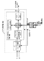
本発明の実施の形態1における誤り訂正回路について、図面を参照しながら説明する。図1は本実施の形態における誤り訂正回路101の構成を示すブロック図である。図1に示す誤り訂正回路101では、太い実線で図示されたブロックが従来例と異なり、図98に示す誤り訂正回路20001のビタビ復号器200002に変えて、切替制御信号で制御されるビタビ復号器102が設けられ、切替制御信号を生成するビタビ復号器制御回路103が加わったことが特徴である。切替制御信号とは、変調方式及び符号化率の切替時にビタビ復号データを出力する際、最小のパスメトリックを判定するためのシンボルをパスメモリ中で切り替えるための信号である。その他の各ブロック、即ち高/低階層選択信号生成回路20003〜選局回路20011が設けられていることは図98に示すものと同一である。
【0151】
以上のように構成された誤り訂正回路101の各ブロックとその動作について以下に説明する。ただし、ビタビ復号器102の出力以降の動作については従来例と同一であるので、それらの説明は省略する。
【0152】
図2は本実施の形態のビタビ復号器102の構成を示すブロック図であり、ビタビ復号器制御回路103も併せて図示している。従来例と異なるブロックを太い実線で示すが、このような図示方法は以下に述べる全てのブロック図で採用するものとする。図2のビタビ復号器102は、デ・パンクチャド・S/P回路20016と、点線部で示すビタビ復号化回路104とを有している。ビタビ復号化回路104は、ブランチメトリック計算回路20018と、ACS回路105と、パスメトリックメモリ20020と、パスメモリ20021とを有している。本実施の形態のビタビ復号器102は、図100に示す従来例のビタビ復号器20002と比較して、ACS回路105の内部構成のみが異なる。
【0153】
図118を用いて説明した発明の解決課題に対して、伝送モードの切替時における本実施の形態のビタビ復号制御方法について説明する。図3は伝送モード切替時におけるビタビ復号器102中のパスメモリ20021(パスメモリ長=J)の様子を示すトレリス線図である。図3(a)は、伝送モードAの最終シンボルまでがパスメモリ20021に入力された時点のトレリス線図である。図3(b)は、次の伝送モードBの第1シンボルがパスメモリ20021に入力された時点のトレリス線図である。図3(c)は、伝送モードBの次の(J−2)シンボルまでがパスメモリ20021に入力された時点のトレリス線図である。
【0154】
図1に示すように、本実施の形態の誤り訂正回路101においては、伝送制御情報復号回路20010において復号された図82の伝送モード/スロット情報がビタビ復号器制御回路103に出力される。ビタビ復号器制御回路103は、入力された伝送モード/スロット情報によって、伝送モードの切替シンボルを認識する。ビタビ復号器制御回路103は、図3(a)の伝送モードAの最終シンボルまでがパスメモリ20021に入力される時点より、図3(c)の伝送モードBの(J−1)シンボルがパスメモリ20021に入力される時点まで切替制御信号を生成してACS回路105に出力する。
【0155】
ACS回路105は、ビタビ復号器制御回路103より出力される切替制御信号により、以下のようにパスメトリックメモリ20020とパスメモリ20021の制御を行う。即ち図3(a)のように、伝送モードAの最終シンボルまでがパスメモリ20021に入力される時点においては、通常のビタビ復号と同じく、パスメモリ20021に入力される最新のシンボル、即ちパスメモリ20021中の第J番目のシンボルの全状態の中で、最小のパスメトリックを有する状態を判定する。その状態に入力している生き残りパスを(J−1)シンボル分前に戻り、該当するパスメモリ20021中の第1番目のシンボルをビタビ復号シンボルデータとして出力する。
【0156】
次に図3(b)のように、伝送モードBの第1シンボルがパスメモリ20021に入力される時点においては、通常のACS動作を行って最新のトレリス線図を生成するべくブランチを1シンボル分伸ばす。ただし、図3(a)の時点で最小のパスメトリックと判定された状態、即ちパスメモリ20021中の第(J−1)番目のシンボルに入力している生き残りパスを(J−2)シンボル分前に戻り、該当するパスメモリ20021中の第1番目のシンボルをビタビ復号シンボルデータとして出力する。
【0157】
以下、パスメモリ20021に伝送モードAの未出力データが残留している期間は、伝送モードAの最終シンボルにおける最小のパスメトリックと判定された状態に入力している生き残りパスより前へ戻り、該当するパスメモリ20021中の第1番目のシンボルをビタビ復号シンボルデータとして出力する。
【0158】
図3(c)は図3(b)よりさらに伝送モードBの(J−2)シンボルがパスメモリ20021に入力される時点のトレリス線図を示す。この時点では、伝送モードAの最終シンボルがパスメモリ20021中の第1番目のシンボルに該当し、最小のパスメトリックと判定された状態に対応するビタビ復号データをパスメモリ20021より出力する。
【0159】
図3(c)よりさらに伝送モードBの次の1シンボルが、パスメモリ20021に入力されると、パスメモリ20021中のデータは全て伝送モードBのシンボルなので、通常のビタビ復号出力の方法を再開する。パスメモリ20021に入力される最新のシンボル、即ちパスメモリ20021中の第J番目のシンボルの全状態の中で、最小のパスメトリックを有する状態を判定する。その状態に入力している生き残りパスを(J−1)シンボル分前に戻り、該当するパスメモリ20021中の第1番目のシンボルをビタビ復号シンボルデータとして出力する。また、ビタビ復号器102は、以上に示した伝送モード切替時の制御以外は、従来例に示したビタビ復号器20002と同様の動作を行ってビタビ復号データを出力する。
【0160】
以上に示した構成により、本実施の形態の誤り訂正回路101は、モード切替後の伝送モードBの影響を完全に遮断して、伝送モード切替時にパスメモリ20021に残留しているモード切替前の伝送モードAのビタビ復号データを出力することができる。
【0161】
また、本実施の形態において、ビタビ復号器制御回路103は切替制御信号を以下に示すように生成し、ACS回路105がビタビ復号器制御回路103より出力される切替制御信号により、図4に示すようにパスメトリックメモリ20020とパスメモリ20021の制御を行ってもよい。この場合、図1のビタビ復号器制御回路103は、伝送制御情報復号回路20010から出力された伝送モード/スロット情報によって、伝送モードの切替シンボルを認識する。図4(a)に示すように、伝送モードAの最終シンボルまでがパスメモリ20021に入力される時点においてのみ、切替制御信号を生成してACS回路105に出力する。
【0162】
図4(a)のように、伝送モードAの最終シンボルまでがパスメモリ20021に入力される時点においては、ACS回路105は通常のビタビ復号と同じく、パスメモリ20021に入力される最新のシンボル、即ちパスメモリ20021中の第J番目のシンボルの全状態の中で、最小のパスメトリックを有する状態を判定する。そして、その状態のみを有効とし、他の状態を全て無効とするように、パスメトリックメモリ20020とパスメモリ20021の制御を行う。
【0163】
その他は、従来例に示したビタビ復号と同様の復号を行う。入力された最新のシンボル、即ちパスメモリ20021中の第J番目のシンボルの全状態の中で、最小のパスメトリックを有する状態を判定する。その状態に入力している生き残りパスを(J−1)シンボル分前に戻り、該当するパスメモリ20021中の第1番目のシンボルをビタビ復号シンボルデータとして出力する。
【0164】
以上に示した構成により、伝送モード切替前の伝送モードAの最終シンボルについては、図4(a)〜(c)に示すトレリス線図において、最小パスメトリックを有する1状態のみを有効とする。従って、本実施の形態の誤り訂正回路101は、モード切替後の伝送モードBの影響を完全に遮断して、伝送モード切替時にパスメモリ20021に残留しているモード切替前の伝送モードAのビタビ復号データを出力することができる。
【0165】
なお、図3(a)〜(c)まで、又は図4(a)の時点において、ビタビ復号器制御回路103が切替制御信号を生成するものとした。しかしながら、伝送モード切替後の変調多値数が伝送モード切替前より大きい場合、又は変調多値数が同じで符号化率が大きい場合のみ切替制御信号を生成する構成にしてもよい。例えば、図89に示す伝送フレームにおいては、TMCC(BPSK:r=1/2)→次の伝送モード(TC−8PSK:r=2/3、又はQPSK:r=3/4、又はQPSK:r=1/2)の伝送モード切替時のみにおいて、ビタビ復号器制御回路103が切替制御信号を生成するものとしてもよい。ただし、TMCC(BPSK:r=1/2)→BPSK(r=1/2)の場合を除く。
【0166】
ビタビ復号器制御回路103で生成される切替制御信号により、伝送モード切替前の伝送モードAは、図3のように最終シンボルにおいて終結して復号されていることになる。しかしながら、例えば主信号のTC−8PSK(r=2/3)→QPSK(r=3/4)の伝送モード切替時においては、TC−8PSK(r=2/3)の最終シンボルに続くQPSK(r=3/4)のシンボルは、図96のように、TC−8PSK(r=2/3)の符号点間距離より大きい符号点間距離を有している。従って、QPSK(r=3/4)の第1シンボルより続けて終結を行わずに通常のビタビ復号を行うと、QPSK(r=3/4)が有するより確からしいブランチメトリックが生成され、終結を行った場合よりもパスメモリ20021に残留したTC−8PSK(r=2/3)の(J−1)シンボル分のBERが低減されることが期待できる。
【0167】
また図87に示すように、TMCC(BPSK:r=1/2)の前後には、2バイトずつ、ビタビ復号器102の入力では20シンボルずつの固定シンボル系列がTAB信号(w1、w2、w3)として存在する。よって、TMCC(BPSK:r=1/2))の前後の伝送モード切替時においては、ビタビ復号器制御回路103は切替制御信号を生成しない構成にしてもよい。この場合には、固定シンボル系列の性質を利用したビタビ復号制御方法が考えられる。これについては実施の形態2、3において説明する。
【0168】
(実施の形態2)
本発明の実施の形態2における誤り訂正回路について、図面を参照しながら説明する。図5は本実施の形態における誤り訂正回路201の構成を示すブロック図である。図5に示す誤り訂正回路201では、太い実線で図示されたブロックが従来例と異なり、図98に示す誤り訂正回路20001のビタビ復号器200002に代えて、確定状態信号で制御されるビタビ復号器202が設けられ、確定状態信号を生成するビタビ復号器制御回路203が加わったことが特徴である。確定状態信号とは、固定シンボル系列について、たたみ込み符号化器の状態が確定する期間を示す信号である。その他の各ブロック、即ち高/低階層選択信号生成回路20003〜選局回路20011が設けられていることは図98に示すものと同一である。
【0169】
以上のように構成された誤り訂正回路201の各ブロックとその動作について説明する。ただし、ビタビ復号器202の出力以降の動作については、従来例で示した通りなので、説明を省略する。
【0170】
図6は本実施の形態のビタビ復号器202の構成を示すブロック図であり、ビタビ復号器制御回路203も併せて図示している。ビタビ復号器202は、デ・パンクチャド・S/P回路20016と、点線部で示すビタビ復号化回路204とを有している。ビタビ復号化回路204は、ブランチメトリック計算回路20018と、ACS回路205と、パスメトリックメモリ20020と、パスメモリ20021とを有している。本実施の形態のビタビ復号器202は、図100に示す従来例のビタビ復号器20002と比較して、ACS回路205の内部構成のみが異なる。
【0171】
図118を用いて説明した発明の解決課題に対して、伝送モードの切替時における本実施の形態のビタビ復号制御について、特にTAB信号の固定シンボル系列の性質を利用した制御方法について、以下に説明する。図7は伝送モード切替時、例えばTMCC(BPSK:r=1/2)→伝送モードBにおけるビタビ復号器202中のパスメモリ20021(パスメモリ長=J)の様子を示すトレリス線図である。
【0172】
特に図7(a)は、TMCC(BPSK:r=1/2)の後ろTAB信号32シンボル、例えば図87、図108に示すw2= xxx0B677h、又はw3= xxxF4988hの内、たたみ込み回路10014の状態が確定する20シンボル中の第1シンボルまでがパスメモリ20021に入力された時点のトレリス線図である。なお、上記のTAB信号の内、たたみ込み回路10014の状態が確定する20シンボルは、デ・パンクチャド・S/P回路20016でS/P変換後では10シンボルに相当する。
【0173】
また図7(b)は、後ろTAB信号の次のシンボル(S/P変換後)がパスメモリ20021に入力された時点のトレリス線図である。さらに図7(c)は、後ろTAB信号の残りのシンボル(S/P変換後の8シンボル)に続き、伝送モードBの最初の(J−10)シンボルがパスメモリ20021に入力された時点のトレリス線図である。
【0174】
本実施の形態の誤り訂正回路201においては、実施の形態1と同様に、伝送制御情報復号回路20010において復号された伝送モード/スロット情報がビタビ復号器制御回路203に出力される。
【0175】
ビタビ復号器制御回路203は、伝送制御情報復号回路20010から出力された伝送モード/スロット情報によって、固定系列シンボルであるTAB信号(w1、w2、w3)を認識する。図7(a)のように、S/P変換後の各TAB信号10シンボルの第1シンボルが、パスメモリ20021に入力される時点より、各TAB信号の第10シンボルがパスメモリ20021に入力される時点まで、確定状態信号を生成してACS回路205に出力する。
【0176】
図6のACS回路205は、ビタビ復号器制御回路203より出力される確定状態信号により、以下のようにパスメトリックメモリ20020とパスメモリ20021の制御を行う。即ち図7(a)の1シンボル前、TMCC(BPSK:r=1/2)の後ろTAB信号32シンボルであるw2= xxx0B677h又はw3= xxxF4988hの内、たたみ込み回路10014の状態が確定する20シンボルの1シンボル前までがパスメモリ20021に入力される時点までは、ACS回路205が通常のビタビ復号と同じく、パスメモリ20021に入力される最新のシンボル、即ちパスメモリ20021中の第J番目のシンボルの全状態の中で、最小のパスメトリックを有する状態を判定する。そしてこの状態に入力している生き残りパスを(J−1)シンボル分前に戻り、該当するパスメモリ20021中の第1番目のシンボルをビタビ復号シンボルデータとして出力する。
【0177】
次に、たたみ込み回路10014の状態が確定する後ろTAB信号(w2又はw3)中の20シンボルの第1シンボルが、パスメモリ20021に入力される時点では、確定した1状態のみを有効とし、他の状態を全て無効とするように、パスメトリックメモリ20020とパスメモリ20021の制御を行う。
【0178】
図7(b)のように、後ろTAB信号(w2又はw3)の次のシンボルがパスメモリ20021に入力される時点でも同様にして、確定した1状態のみを有効とし、他の状態を全て無効とするように、パスメトリックメモリ20020とパスメモリ20021の制御を行う。同様の制御を、後ろTAB信号の残りのシンボルが入力される時点まで行う。
【0179】
次に、伝送モードBの第1シンボルが入力されると、従来例に示したビタビ復号と同様な復号を行う。入力された最新のシンボル、即ちパスメモリ20021中の第J番目のシンボルの全状態の中で、最小のパスメトリックを有する状態を判定する。その状態に入力している生き残りパスを(J−1)シンボル分前に戻し、該当するパスメモリ20021中の第1番目のシンボルをビタビ復号シンボルデータとして出力する。なお、図7(c)は、伝送モードBの最初の(J−10)シンボルまでが、パスメモリ20021に入力された時点を示している。
【0180】
以上は、後ろTAB信号(w2又はw3)における固定シンボル系列の性質を利用したビタビ復号制御方法であるが、前TAB信号(w1)についても同様の制御を行うことができる。
【0181】
また、ビタビ復号器202は、以上に示した伝送モード切替時、即ちTMCC(BPSK:r=1/2)→伝送モードBの制御以外は、従来例に示したビタビ復号器20002と同様の動作を行ってビタビ復号データを出力するものとする。
【0182】
以上に示した構成により、伝送モード切替前のTMCC(BPSK:r=1/2)の後ろTAB信号(w2又はw3)における固定シンボル系列の性質を利用したビタビ復号制御を行うようにしている。従って、本実施の形態の誤り訂正回路201は、モード切替後の伝送モードBの影響を完全に遮断して、伝送モード切替時にパスメモリ20021に残留しているモード切替前のTMCC(BPSK:r=1/2)のビタビ復号データを出力することができる。
【0183】
後ろTAB信号(w2又はw3)の固定シンボル系列20シンボル(S/P変換後は10シンボル)については、上記の制御方法によって常に正しいビタビ復号データが選択される。その結果、図7(a)に示すように後ろTAB信号(w2又はw3)の第1シンボルがパスメモリ20021に入力された時点において、パスメモリに残留しているTMCC(BPSK:r=1/2)(J−1)シンボルの誤り率を低減することが可能である。
【0184】
また、前TAB信号(w1)の固定シンボル系列20シンボルについても、同様のビタビ復号制御を行うことにより、TMCC(BPSK:r=1/2)のモード切替前の伝送モードTC−8PSK(r=2/3)又はQPSK(r=3/4、1/2)又はBPSK(r=1/2)の影響を遮断することができる。
【0185】
以上に示したように、本実施の形態の誤り訂正回路201は、前TAB信号(w1)と後ろTAB信号(w2又はw3)の固定シンボル系列それぞれ20シンボル(S/P変換後は10シンボル)を利用したビタビ復号制御方法を行うことにより、図108(a)に示すTMCC(BPSK:r=1/2)の実シンボルデータ128シンボル(S/P変換後は64シンボル)については、前後の伝送モードのシンボルの影響を完全に遮断し、BPSK(r=1/2)の本来有しているたたみ込み符号化の誤り訂正能力を引き出すことができる。
【0186】
なお、本実施の形態においては、ビタビ復号器制御回路203は、図7(a)のように各TAB信号(w1、w2、w3)20シンボル(S/P変換後は10シンボル)の第1シンボルが、パスメモリ20021に入力される時点より、各TAB信号の第10シンボル(S/P変換後の最終シンボル)がパスメモリ20021に入力される時点まで確定状態信号を生成して、ACS回路205に出力する構成とした。その代わりに、ビタビ復号器制御回路203は、例えば各TAB信号20シンボル(S/P変換後は10シンボル)の第1シンボルがパスメモリ20021に入力される時点のみ確定状態信号を生成して、ACS回路205に出力する構成としてもよい。この構成を取ることにより、ビタビ復号器制御回路203とACS回路205の制御を簡単化することができる。各TAB信号の第1シンボル(S/P変換後の最終シンボル)については、図7に示すトレリス線図において、確定された1状態のみが有効とされ、他の全状態は無効とされるので、少なくともTMCC(BPSK:r=1/2)の前後の伝送モードのシンボルの影響を遮断することは可能である。
【0187】
なお上記では、ビタビ復号器制御回路203は、例えば各TAB信号20シンボルの第1シンボルがパスメモリ20021に入力される時点のみ確定状態信号を生成して、ACS回路205に出力するようにした。しかし、図7(a)〜(c)に示すようにS/P変換後では、確定状態信号を生成するシンボル期間は、1シンボル以上、最大10シンボルまでの間で任意に選択可能であり、どのシンボルを選択するかも任意である。
【0188】
(実施の形態3)
本発明の実施の形態3における誤り訂正回路について、図面を参照しながら説明する。図8は本実施の形態における誤り訂正回路301の構成を示すブロック図である。図8に示す誤り訂正回路301では、太い実線で図示されたブロックが従来例と異なり、図98の誤り訂正回路20001のビタビ復号器200002に代えて、固定ブランチ信号で制御されるビタビ復号器302が設けられ、固定ブランチ信号を生成するビタビ復号器制御回路303が加わったことが特徴である。固定ブランチ信号とは、固定シンボル系列についてトレリス線図の状態遷移におけるブランチを特定する信号である。その他の各ブロック、即ち高/低階層選択信号生成回路20003〜選局回路20011が設けられていることは図98に示すものと同一である。
【0189】
以上のように構成された誤り訂正回路301の各ブロックとその動作について説明する。ただし、ビタビ復号器302の出力以降の動作については、従来例で示した通りなので、説明を省略する。
【0190】
図9は本実施の形態のビタビ復号器302の構成を示すブロック図であり、ビタビ復号器制御回路303も併せて図示している。ビタビ復号器302は、デ・パンクチャド・S/P回路20016と、点線部で示すビタビ復号化回路304とを有している。ビタビ復号化回路304は、ブランチメトリック計算回路20018と、ACS回路305と、パスメトリックメモリ20020と、パスメモリ20021とを有している。本実施の形態のビタビ復号器302は、図100の従来例のビタビ復号器20002と比較して、ACS回路305の内部構成のみが変わっている。
【0191】
図118を用いて説明した発明の解決課題に対して、伝送モードの切替時における本実施の形態のビタビ復号制御方法について、特にTAB信号の固定シンボル系列の性質を利用した制御方法について以下に説明する。
【0192】
図10はビタビ復号におけるブランチの出力方法を示すトレリス線図である。ここでは、ビタビ復号シンボルが1シンボル=1ビットのQPSK(r=3/4、1/ 2)、又はBPSK(r=1/2)である場合を示している。図10(a)は従来のビタビ復号におけるブランチの出力方法を示すトレリス線図である。時刻tにおいて、各状態より復号推定シンボル“1”と“0”に対応する2つのブランチを出力する。図10(a)のように、時刻(t+1)においては状態Sに入力されるブランチは2つあり、従来例で示したビタビ復号器20002はその中から最小のパスメトリックを有するブランチ(太線で示す)を生き残りパスとしていた。
【0193】
一方、図10(b)はTAB信号に対して本実施の形態のビタビ復号におけるブランチの出力方法を示すトレリス線図である。例えば、後ろTAB信号(w2=xxx0B677h 、復号データW2=A340h )が図9のビタビ復号器302に入力される場合については、復号推定シンボルの計16シンボルについて、それぞれの復号推定シンボルは“1”か“0”かが既知である。例えば、第1シンボル=“1”とする。従って、図10(b)に示すように、例えば後ろTAB信号(w2)の第1シンボルについては、時刻tにおいて、各状態より復号推定シンボル“1”に対応する1つのブランチのみを出力する。時刻(t+1)においては、状態Sに入力されるブランチは1つのみであり、図10(b)の太線のように自動的に生き残りパスが決定される。
【0194】
図10(a)と図10(b)を比較すると、図10(b)ではTAB信号区間については、各状態より1つのブランチ、例えば復号推定シンボル=“1”に対応するブランチのみを出力するため、時刻(t+1)において各状態に入力するブランチは、復号推定シンボル=“1”に対応するブランチであり、それが自動的に生き残りパスを決定する。従って、TAB信号区間について誤った系列を生き残りパスとすることがなく、TMCC(BPSK:r=1/2)に続く伝送モードBの影響を遮断して、伝送モード切替時にパスメモリ20021に残留しているTMCCのビタビ復号データを出力することができる。一方、図10(a)では、TAB信号が有する固定シンボル系列の性質を利用せず、時刻(t+1)においては各状態に入力されるブランチは2つあり、誤った復号推定シンボルに対応するブランチが、生き残りパスとして選択される可能性がある。
【0195】
ここで、図10(b)に示したTAB信号区間(固定系列区間)におけるビタビ復号制御方法を次に説明する。図8の誤り訂正回路301においては、実施の形態1と同様に、伝送制御情報復号回路20010において復号された図82の伝送モード/スロット情報がビタビ復号器制御回路303に出力される。ビタビ復号器制御回路303はこの伝送モード/スロット情報によって固定系列シンボル(TAB信号:w1、w2、w3)を認識する。各TAB信号16シンボルの第1シンボルがパスメモリ20021に入力される時点より、各TAB信号の第16シンボルがパスメモリ20021に入力される時点まで固定ブランチ信号を生成してACS回路305に出力する。
【0196】
ACS回路305は、ビタビ復号器制御回路303より出力される固定ブランチ信号により、トレリス線図の各状態より、固定系列=“1”あるいは“0”に対応した1つのブランチのみを出力するようにパスメトリックメモリ20020とパスメモリ20021の制御を行う。
【0197】
また、ビタビ復号器302は、以上に示した伝送モード切替時、即ちTMCC(BPSK:r=1/2)→伝送モードBの制御以外は、従来例に示したビタビ復号器20002と同様の動作を行ってビタビ復号データを出力する。
【0198】
以上に示した構成により、伝送モード切替前のTMCC(BPSK:r=1/2)の後ろTAB信号(w2、w3)の固定シンボル系列の性質を利用したビタビ復号制御を行う。従って、本実施の形態の誤り訂正回路301は、モード切替後の伝送モードBの影響を遮断して、伝送モード切替時にパスメモリ20021に残留しているモード切替前のTMCC(BPSK:r=1/2)のビタビ復号データを出力することができる。
【0199】
その結果、パスメモリ長=Jとすると、後ろTAB信号(w2、w3)の第1シンボルがパスメモリ20021に入力された時点において、パスメモリに残留しているTMCC(BPSK:r=1/2)(J−1)シンボルの誤り率を低減することが可能である。また、前TAB信号(w1)の固定シンボル系列16シンボルについても、同様のビタビ復号制御を行うことにより、TMCC(BPSK:r=1/2)のモード切替前の伝送モード、即ちTC−8PSK(r=2/3)又はQPSK(r=3/4、1/2)、又はBPSK(r=1/2)の影響を遮断することができる。
【0200】
以上に示したように、本実施の形態の誤り訂正回路301は、前TAB信号(w1)と後ろTAB信号(w2、w3)の固定シンボル系列をそれぞれ16シンボル利用したビタビ復号制御方法を行うことにより、図108(a)に示すようなTMCC(BPSK:r=1/2)の実シンボルデータ128シンボルについては(S/P変換後は、64シンボル)、前後の伝送モードのシンボルの影響を遮断し、BPSK(r=1/2)の本来有しているたたみ込み符号化の誤り訂正能力を引き出すことができる。
【0201】
(実施の形態4)
本発明の実施の形態4における誤り訂正回路について、図面を参照しながら説明する。図11は本実施の形態における誤り訂正回路401の構成を示すブロック図である。図11に示す誤り訂正回路401では、太い実線で図示されたブロックが従来例と異なり、図98の誤り訂正回路20001のビタビ復号器200002に代えて、状態削減信号で制御されるビタビ復号器402が設けられ、状態削減信号を生成するビタビ復号器制御回路403が加わったことが特徴である。状態削減信号とは、固定シンボル系列についてトレリス線図の状態数を削減する信号である。その他の各ブロック、即ち高/低階層選択信号生成回路20003〜選局回路20011が設けられていることは図98に示すものと同一である。
【0202】
以上のように構成された誤り訂正回路401の各ブロックとその動作について説明する。ただし、ビタビ復号器402の出力以降の動作については、従来例で示した通りなので説明を省略する。
【0203】
図12は本実施の形態のビタビ復号器402の構成を示すブロック図であり、ビタビ復号器制御回路403も併せて図示されている。ビタビ復号器402は、デ・パンクチャド・S/P回路20016と、点線部で示すビタビ復号化回路404とを有している。ビタビ復号化回路404は、ブランチメトリック計算回路20018と、ACS回路405と、パスメトリックメモリ20020と、パスメモリ20021とを有している。本実施の形態のビタビ復号器402は、従来例におけるビタビ復号器20002と比較して、ACS回路405の内部構成のみが変わっている。
【0204】
図118を用いて説明した発明の解決課題に対して、伝送モードの切替時における本実施の形態のビタビ復号制御方法について、特にTAB信号の固定シンボル系列の性質を利用した制御方法について説明する。図13は本実施の形態におけるトレリス線図の状態削減方法を示す説明図である。図中の□は図91に示すたたみ込み回路10014の各レジスタを示し、例として後ろTAB信号(w2=xxx0B677h 、W2=A340h )が各レジスタに入力される場合を示している。
【0205】
図13において、後ろTAB信号w2の16シンボルがビタビ復号化回路404に入力する直前までは、たたみ込み回路10014の全6レジスタの中身が不定であるため、トレリス線図の状態数は図13(a)に示すように64である。w2の第1シンボルがビタビ復号化回路404に入力されると、最初のレジスタの中身が“1”と決まるので、状態数は図13(b)のように32に削減される。次に、w2の第2シンボルがビタビ復号化回路404に入力されると、最初の2つのレジスタの中身が“01”と決まるので、状態数は図13(c)のように16に削減される。
【0206】
以下、1シンボルずつビタビ復号化回路404に入力される毎に状態数が半減し、w2の第6シンボルまでがビタビ復号化回路404に入力されると、全6つのレジスタの中身が“000101”と決まるので、図13(g)のように1状態に確定する。以降、w2の第16シンボルが入力されるまで、確定した1状態のみが有効となり、ビタビ復号化回路404がビタビ復号を行う。
【0207】
ところで、実施の形態2では、図7のように例えばw2の後ろ10シンボルについてのみ、確定した1状態のみを有効としてビタビ復号を行っていた。それと比較して本実施の形態では、例えばw2の後ろ10シンボルを確定した1状態のみを有効とし、更に先頭6シンボルについて、1シンボルずつビタビ復号化回路404に入力される毎に状態数を半減させている。従って、TAB信号16シンボル(S/P変換後)全てについて、固定系列の性質を利用して伝送モード切替時のビタビ復号制御を行っていることになる。
【0208】
ここで、図13に示したTAB信号区間(固定系列区間)におけるビタビ復号制御の実現方法について説明する。本実施の形態の誤り訂正回路401においては、実施の形態1と同様に伝送制御情報復号回路20010において復号された、伝送モード/スロット情報がビタビ復号器制御回路403に出力される。ビタビ復号器制御回路403はこの伝送モード/スロット情報によって固定系列シンボル(TAB信号:w1、w2、w3)を認識する。各TAB信号16シンボルの第1シンボルが、パスメモリ20021に入力される時点より、各TAB信号の第16シンボルがパスメモリ20021に入力される時点まで状態削減信号を生成してACS回路405に出力する。
【0209】
ACS回路405は、ビタビ復号器制御回路403より出力される状態削減信号により、上述のように各TAB信号の先頭6シンボルについて、1シンボルずつ状態数を半減させ、その後の10シンボルについては確定した1状態のみを有効とするように、パスメトリックメモリ20020とパスメモリ20021の制御を行う。また、ビタビ復号器402は、以上に示した伝送モード切替時、即ちTMCC(BPSK:r=1/2)→伝送モードBの制御以外は、従来例のビタビ復号器20002と同様の動作を行って、ビタビ復号データを出力する。
【0210】
以上に示した構成により、伝送モード切替前のTMCC(BPSK:r=1/2)の後ろTAB信号(w2、w3)の固定シンボル系列の性質を利用したビタビ復号制御を行う。従って、本実施の形態の誤り訂正回路401は、モード切替後の伝送モードBの影響を遮断して、伝送モード切替時にパスメモリ20021に残留しているモード切替前のTMCC(BPSK:r=1/2)のビタビ復号データを出力することができる。
【0211】
その結果、後ろTAB信号(w2、w3)の第1シンボルがパスメモリ20021に入力された時点において、パスメモリに残留しているTMCC(BPSK:r=1/2)(J−1)シンボルの誤り率を低減することが可能である。また、前TAB信号(w1)の固定シンボル系列16シンボルについても、同様のビタビ復号制御を行うことにより、TMCC(BPSK:r=1/2)のモード切替前の伝送モード、即ちTC−8PSK(r=2/3)又はQPSK(r=3/4、1/2)又はBPSK(r=1/2)の影響を遮断することができる。
【0212】
以上に示したように、本実施の形態の誤り訂正回路401は、前TAB信号(w1)と後ろTAB信号(w2、w3)の固定シンボル系列それぞれ16シンボル(S/P変換後)を利用したビタビ復号制御方法を行うことにより、図108(a)に示すTMCC(BPSK:r=1/2)の実シンボルデータ128シンボルについては(S/P変換後は、64シンボル)、前後の伝送モードのシンボルの影響を遮断し、BPSK(r=1/2)の本来有しているたたみ込み符号化の誤り訂正能力を引き出すことができる。
【0213】
更に図13に示すように、先頭6シンボルについて、1シンボルずつパスメモリ20021に入力される毎に、状態数を半減させている。従って、TAB信号16シンボル全てについて、固定系列の性質を利用して伝送モード切替時のビタビ復号制御を行っていることになり、実施の形態2と3に比べて、TMCC(BPSK:r=1/2)の実シンボルデータの誤り率をより低減することができる。
【0214】
(実施の形態5)
本発明の実施の形態5における誤り訂正回路について、図面を参照しながら説明する。図14は本実施の形態における誤り訂正回路501の構成を示すブロック図である。この誤り訂正回路501では、太い実線で図示されたブロックが従来例と異なり、図98に示す誤り訂正回路20001に対して、シンボル座標変換信号を生成するビタビ復号器制御回路503と、シンボル座標変換信号で制御される入力シンボル変換回路506とが加わったことが特徴である。シンボル座標変換信号とは、固定シンボルに対応した復調I/Qデータに変換する信号である。その他の各ブロック、即ちビタビ復号器20002、高/低階層選択信号生成回路20003〜選局回路20011が設けられていることは図98に示すものと同一である。
【0215】
以上のように構成された誤り訂正回路501の各ブロックとその動作について説明する。ただし、ビタビ復号器20002の出力以降の動作については、従来例で示した通りなので、説明を省略する。
【0216】
図15はビタビ復号器20002の構成と、ビタビ復号器20002及びビタビ復号器制御回路303と入力シンボル変換回路506との接続関係を示すブロック図である。本実施の形態のビタビ復号器20002は、図100の従来例のビタビ復号器の構成と同じである。
【0217】
図118を用いて説明した発明の解決課題に対して、伝送モードの切替時における本実施の形態のビタビ復号制御方法ついて、特にTAB信号の固定シンボル系列の性質を利用した制御方法について説明する。本実施の形態の誤り訂正回路501においては、実施の形態1と同様に、伝送制御情報復号回路20010で復号された伝送モード/スロット情報がビタビ復号器制御回路503に出力される。ビタビ復号器制御回路503は、この伝送モード/スロット情報によって固定系列シンボルであるTAB信号(w1、w2、w3)を認識する。図87又は図108に示すように、TMCC(BPSK:r=1/2)の後ろTAB信号32シンボル(w2= xxx0B677h、又はw3= xxxF4988h)の内、たたみ込み回路10014の状態が確定する後ろ20シンボルが入力シンボル変換回路506に入力される区間については、シンボル座標変換信号を生成して入力シンボル変換回路506に出力する。
【0218】
入力シンボル変換回路506は、ビタビ復号器制御回路503より出力されるシンボル座標変換信号に従って、たたみ込み回路10014の状態が確定する後ろ20シンボルをその符号点のI/Qデータに変換し、それ以外の入力シンボルについてはそのままのI/Qデータでビタビ復号器20002に出力する。
【0219】
図87又は図108に示すように、TMCC(BPSK:r=1/2)の前TAB信号32シンボル(w1= xxxECD28h)の内、たたみ込み回路10014の状態が確定する後ろ20シンボルについても、入力シンボル変換回路506は同様なI/Q座標変換を行う。
【0220】
入力シンボル変換回路506におけるI/Qデータの変換の様子を図16に示す。入力シンボル変換回路506は、図示しないPSK復調器からの出力された入力シンボルのI/Q座標を、TAB信号の内、たたみ込み回路10014の状態が確定する後ろ20シンボルについて、そのシンボルが“0”、あるいは“1”の固定シンボルであるかによって、図16のように“0”、あるいは“1”の符号点のI/Q座標データに変換する。そしてビタビ復号器20002は従来例と同じようにビタビ復号を行い、ビタビ復号データをシンボル/バイト変換回路20004に出力する。
【0221】
上記に示した通り、TAB信号の内、たたみ込み回路10014の状態が確定する後ろ20シンボルについては、符号点と距離が0のI/Q座標がビタビ復号器20002に入力されることになる。即ち、ビタビ復号のトレリス線図において、たたみ込み回路10014の状態が確定する後ろ20シンボルについては、変換された符号点の正しい1状態に入力するブランチメトリックは0で、他の全状態は非常に大きなブランチメトリックが生成される。このような復号方法では、図7(a)〜(c)に示す実施の形態2のビタビ復号制御方法と等価的な制御が行われていると見なすことができる。即ち、確定された1状態(変換された符号点の状態)に入力するブランチメトリックと比較して、他の全状態に入力するブランチメトリックはその値が非常に大きいため、確定された1状態が最小のパスメトリックと自動的に判定されることになる。
【0222】
以上に示したように、本実施の形態の誤り訂正回路501は、前TAB信号(w1)と後ろTAB信号(w2又はw3)の固定シンボル系列それぞれ20シンボルを利用したビタビ復号制御方法を行うことにより、TMCC(BPSK:r=1/2)の実シンボルデータ、即ち図108(a)に示す128シンボルについては、前後の伝送モードのシンボルの影響を完全に遮断し、BPSK(r=1/2)の本来有しているたたみ込み符号化の誤り訂正能力を引き出すことができる。
【0223】
本実施の形態では、ビタビ復号器20002の前段に入力シンボル変換回路506を設ける構成にしているので、図14のビタビ復号器20002は従来例のビタビ復号器をそのまま用いることができる。
【0224】
シミュレーションにより、本実施の形態の誤り訂正回路501の機能
(効果)を調べた。図17はシミュレーションに用いた伝送フレームの構成図である。図17(a)は入力シンボル変換回路506への入力形式を示し、TMCCはS/P変換前の信号である。図17(b)はパスメモリ20021への入力形式を示し、TMCCはS/P変換後の信号である。パスメモリ長は64とし、TMCCの後の主信号はTC−8PSK(r=2/3)64シンボルのみとした。この64シンボルの主信号により、TMCCの第1シンボルが入力される直前では、パスメモリ20021はTC−8PSK(r=2/3)64シンボルで満たされている状態になる。
【0225】
図18は上記の条件でシミュレーションした復号結果のBERである。C/N=−1dBとし、パスメモリ20021に後ろTAB信号(w2又はw3)の最終シンボルが入力された時点において、パスメモリ20021に残留している64シンボルについて、1シンボル毎のBERを算出した。横軸はパスメモリ20021に残留している64シンボルを示し、縦軸はBERを示す。この図より明らかなように、本実施の形態の「終結処理あり」は、従来例の「終結処理なし」と比較して、パスメモリ20021に残留している各シンボルの誤り率が改善されていることが判る。
【0226】
(実施の形態6)
本発明の実施の形態6における誤り訂正回路について、図面を参照しながら説明する。図19は本実施の形態における誤り訂正回路601の構成を示すブロック図である。図19に示す誤り訂正回路601では、太い実線で図示されたブロックが従来例と異なっている。即ち、図98の誤り訂正回路20001のビタビ復号器200002に代えて、固定ブランチ信号及び確定状態信号で制御されるビタビ復号器102が設けられ、固定ブランチ信号及び確定状態信号を生成するビタビ復号器制御回路603が新たに加わったことが特徴である。その他の各ブロック、即ち高/低階層選択信号生成回路20003〜選局回路20011が設けられていることは、図98に示すものと同一である。
【0227】
以上のように構成された誤り訂正回路601の動作について説明する。ただし、ビタビ復号器602の出力以降の動作については従来例で示した通りなので、説明を省略する。
【0228】
図20はビタビ復号器602の構成を示すブロック図であり、ビタビ復号器制御回路603も併せて図示している。ビタビ復号器602は、デ・パンクチャド・S/P回路20016と、点線部で示すビタビ復号化回路604とを有している。ビタビ復号化回路604は、ブランチメトリック計算回路20018と、ACS回路605と、パスメトリックメモリ20020と、パスメモリ20021とを有している。本実施の形態のビタビ復号器602は、図6に示す実施の形態2におけるビタビ復号器202と比較して、ACS回路605の内部構成のみが変わっている。
【0229】
図118を用いて説明した発明の解決課題に対して、伝送モードの切替時における本実施の形態のビタビ復号制御方法について、特にTAB信号の固定シンボル系列の性質を利用した制御方法について説明する。本実施の形態の誤り訂正回路601においては、実施の形態1と同様に、伝送制御情報復号回路20010において復号された伝送モード/スロット情報がビタビ復号器制御回路603に出力される。ビタビ復号器制御回路603は、実施の形態2と同様にして、伝送モード/スロット情報によって、固定系列シンボルであるTAB信号(w1、w2、w3)を認識する。図7(a)に示すように、各TAB信号の後ろ10シンボルの第1シンボルがパスメモリ20021に入力される時点より、各TAB信号の第10シンボルがパスメモリ20021に入力される時点まで、確定状態信号を生成してACS回路605に出力する。
【0230】
ACS回路605は図7(a)〜(c)に示すように、ビタビ復号器制御回路603より出力される確定状態信号により、実施の形態2と同様にしてパスメトリックメモリ20020とパスメモリ20021の制御を行う。また、ビタビ復号器制御回路603は、各TAB信号の先頭6シンボル、即ちたたみ込み回路10014が1状態に確定するまでの信号がパスメモリ20021に入力される区間について、固定ブランチ信号を生成してACS回路605に出力する。
【0231】
ACS回路605は図10(b)に示すように、ビタビ復号器制御回路603より出力される固定ブランチ信号により、各TAB信号の先頭6シンボルについては、実施の形態3と同様にしてパスメトリックメモリ20020とパスメモリ20021の制御を行う。また、ビタビ復号器602は、以上に示した伝送モード切替時、即ちTMCC(BPSK:r=1/2)→伝送モードBの制御以外は、従来例に示したビタビ復号器20002と同様の動作を行って、ビタビ復号データを出力する。
【0232】
以上に示した構成により、実施の形態2と同様に、伝送モード切替前のTMCC(BPSK:r=1/2)のTAB信号(w1、w2又はw3)の固定シンボル系列の性質を利用したビタビ復号制御を行う。従って、本実施の形態の誤り訂正回路601は、モード切替後の伝送モードBの影響を完全に遮断して、伝送モード切替時にパスメモリ20021に残留しているモード切替前のTMCC(BPSK:r=1/2)のビタビ復号データを出力することができる。かつ、TMCC(BPSK:r=1/2)のモード切替前の伝送モードの影響も完全に遮断することができる。
【0233】
更に、本実施の形態においては、各TAB信号の先頭6シンボルについて、固定ブランチ信号によるビタビ復号制御を行う。従って、TAB信号16シンボル全てについて、固定系列の性質を利用して、伝送モード切替時のビタビ復号制御を行っていることになり、実施の形態2と比較して、TMCC(BPSK:r=1/2)の実シンボルデータの誤り率をより低減することができる。
【0234】
(実施の形態7)
本発明の実施の形態7における誤り訂正回路について、図面を参照しながら説明する。図21は本実施の形態における誤り訂正回路701の構成を示すブロック図である。図21に示す誤り訂正回路701では、太い実線で図示されたブロックが従来例と異なり、図98の誤り訂正回路20001のビタビ復号器200002に代えて、固定ブランチ信号で制御されるビタビ復号器702が設けられ、固定ブランチ信号及びシンボル座標変換信号を生成するビタビ復号器制御回路703と、シンボル座標変換信号で制御される入力シンボル変換回路506が新たに加わったことが特徴である。その他の各ブロック、即ち高/低階層選択信号生成回路20003〜選局回路20011が設けられていることは、図98に示すものと同一である。
【0235】
以上のように構成された誤り訂正回路701の各ブロックとその動作について説明する。ただし、ビタビ復号器702の出力以降の動作については、従来例で示した通りなので説明を省略する。
【0236】
図22はビタビ復号器702の構成を示すブロック図であり、ビタビ復号器制御回路703と入力シンボル変換回路506とを併せて図示している。ビタビ復号器702は、デ・パンクチャド・S/P回路20016と、点線部で示すビタビ復号化回路704とを有している。ビタビ復号化回路704は、ブランチメトリック計算回路20018と、ACS回路705と、パスメトリックメモリ20020と、パスメモリ20021とを有している。本実施の形態のビタビ復号器702は、図15に示す実施の形態5のビタビ復号器20002と比較して、ACS回路705の内部構成のみが変わっている。
【0237】
図118を用いて説明した発明の解決課題に対して、伝送モードの切替時における本実施の形態のビタビ復号制御方法について、特にTAB信号の固定シンボル系列の性質を利用した制御方法について説明する。本実施の形態の誤り訂正回路701においては、実施の形態1と同様に、伝送制御情報復号回路20010において復号された伝送モード/スロット情報がビタビ復号器制御回路703に出力される。ビタビ復号器制御回路703は、伝送モード/スロット情報によって固定系列シンボルであるTAB信号(w1、w2、w3)を認識する。図87又は図108に示すように、TMCC(BPSK:r=1/2)の後ろTAB信号32シンボル(w2= xxx0B677h、又はw3= xxxF4988h)の内、たたみ込み回路10014の状態が確定する後ろ20シンボルが、入力シンボル変換回路506に入力される区間については、シンボル座標変換信号を生成して、入力シンボル変換回路506に出力する。
【0238】
入力シンボル変換回路506は、実施の形態5と同様の動作を行って、I/Qデータをビタビ復号器702に出力する。また、ビタビ復号器制御回路703は、各TAB信号の先頭6シンボル、即ちたたみ込み回路10014の1状態に確定するまでがパスメモリ20021に入力される区間について、固定ブランチ信号を生成してACS回路705に出力する。そしてACS回路705は、ビタビ復号器制御回路703より出力される固定ブランチ信号により、各TAB信号の先頭6シンボルについては、実施の形態3と同様にして、パスメトリックメモリ20020とパスメモリ20021の制御を行う。また、ビタビ復号器702は、以上に示した伝送モード切替時、即ちTMCC(BPSK:r=1/2)→伝送モードBの制御以外は、従来例に示したビタビ復号器20002と同様の動作を行って、ビタビ復号データを出力する。
【0239】
以上に示した構成により、実施の形態5と同様に、伝送モード切替前のTMCC(BPSK:r=1/2)のTAB信号(w1、w2又はw3)の固定シンボル系列の性質を利用したビタビ復号制御を行う。従って、本実施の形態の誤り訂正回路701は、モード切替後の伝送モードBの影響を遮断して、伝送モード切替時にパスメモリ20021に残留しているモード切替前のTMCC(BPSK:r=1/2)のビタビ復号データを出力することができる。かつ、TMCC(BPSK:r=1/2)のモード切替前の伝送モードの影響も遮断することができる。
【0240】
更に、本実施の形態においては、各TAB信号の先頭6シンボルについて、固定ブランチ信号によるビタビ復号制御を行う。従って、TAB信号16シンボル全てについて、固定系列の性質を利用して伝送モード切替時のビタビ復号制御を行っていることになり、実施の形態5と比較して、TMCC(BPSK:r=1/2)の実シンボルデータの誤り率をより低減することができる。
【0241】
(実施の形態8)
本発明の実施の形態8における誤り訂正回路について、図面を参照しながら説明する。図23は本実施の形態における誤り訂正回路801の構成を示すブロック図である。図23に示す誤り訂正回路801では、太い実線で図示されたブロックが従来例と異なり、図98の誤り訂正回路20001のビタビ復号器200002に代えて、状態削減信号及び確定状態信号で制御されるビタビ復号器802が設けられ、状態削減信号及び確定状態信号を生成するビタビ復号器制御回路803が新たに加わったことが特徴である。その他の各ブロック、即ち高/低階層選択信号生成回路20003〜選局回路20011が設けられていることは、図98に示すものと同一である。
【0242】
以上のように構成された誤り訂正回路801の各ブロックとその動作について説明する。ただし、ビタビ復号器802の出力以降の動作については、従来例で示した通りなので説明を省略する。
【0243】
図24はビタビ復号器802の構成を示すブロック図であり、ビタビ復号器制御回路803も併せて図示されている。ビタビ復号器802は、デ・パンクチャド・S/P回路20016と、点線部で示すビタビ復号化回路804とを有している。ビタビ復号化回路804は、ブランチメトリック計算回路20018と、ACS回路805と、パスメトリックメモリ20020と、パスメモリ20021とを有している。本実施の形態のビタビ復号器802は、図6に示す実施の形態2におけるビタビ復号器202と比較して、ACS回路805の内部構成のみが変わっている。
【0244】
図118を用いて説明した発明の解決課題に対して、伝送モードの切替時における本実施の形態のビタビ復号制御方法について、特にTAB信号の固定シンボル系列の性質を利用した制御方法について説明する。本実施の形態の誤り訂正回路801においては、実施の形態1と同様に、伝送制御情報復号回路20010において復号された伝送モード/スロット情報がビタビ復号器制御回路803に出力される。
【0245】
ビタビ復号器制御回路803は、実施の形態2と同様にして、伝送制御情報復号回路20010から出力された伝送モード/スロット情報によって、固定系列シンボルであるTAB信号(w1、w2、w3)を認識する。図7(a)に示すように、各TAB信号の後ろ10シンボルの第1シンボルが、パスメモリ20021に入力される時点より、各TAB信号の第10シンボルがパスメモリ20021に入力される時点まで確定状態信号を生成してACS回路805に出力する。
【0246】
ACS回路805は、図7(a)〜(c)に示すように、ビタビ復号器制御回路803より出力される確定状態信号により、実施の形態2と同様にしてパスメトリックメモリ20020とパスメモリ20021の制御を行う。また、ビタビ復号器制御回路803は、各TAB信号の先頭6シンボル、即ちたたみ込み回路10014が1状態に確定するまで、がパスメモリ20021に入力される区間について、状態削減信号を生成してACS回路805に出力する。
【0247】
ACS回路805は、ビタビ復号器制御回路803より出力される状態削減信号により、各TAB信号の先頭6シンボルについては、実施の形態4と同様にして、パスメトリックメモリ20020とパスメモリ20021の制御を行い、図13に示すように、たたみ込み回路10014が1状態に確定するまで状態数を半分ずつに削減する。また、ビタビ復号器802は、以上に示した伝送モード切替時、即ちTMCC(BPSK:r=1/2)→伝送モードBの制御以外は、従来例のビタビ復号器20002と同様の動作を行って、ビタビ復号データを出力する。
【0248】
以上に示した構成により、実施の形態2と同様に、伝送モード切替前のTMCC(BPSK:r=1/2)のTAB信号(w1、w2又はw3)の固定シンボル系列の性質を利用したビタビ復号制御を行う。従って、本実施の形態の誤り訂正回路801は、モード切替後の伝送モードBの影響を完全に遮断して、伝送モード切替時にパスメモリ20021に残留しているモード切替前のTMCC(BPSK:r=1/2)のビタビ復号データを出力することができる。かつ、TMCC(BPSK:r=1/2)のモード切替前の伝送モードの影響も完全に遮断する。
【0249】
更に、本実施の形態においては、各TAB信号の先頭6シンボルについて、状態削減信号によるビタビ復号制御を行う。従って、TAB信号16シンボル全てについて、固定系列の性質を利用して、伝送モード切替時のビタビ復号制御を行っていることになり、実施の形態2と比較して、TMCC(BPSK:r=1/2)の実シンボルデータの誤り率をより低減することができる。
【0250】
(実施の形態9)
本発明の実施の形態9における誤り訂正回路について、図面を参照しながら説明する。図25は本実施の形態における誤り訂正回路901の構成を示すブロック図である。図25に示す誤り訂正回路901では、太い実線で図示されたブロックが従来例と異なり、図98の誤り訂正回路20001のビタビ復号器200002に代えて、状態削減信号及び固定ブランチ信号で制御されるビタビ復号器902が設けられ、状態削減信号及び固定ブランチ信号を生成するビタビ復号器制御回路903が新たに加わったことが特徴である。その他の各ブロック、即ち高/低階層選択信号生成回路20003〜選局回路20011が設けられていることは、図98に示すものと同一である。
【0251】
以上のように構成された誤り訂正回路901の各ブロックとその動作について説明する。ただし、ビタビ復号器902の出力以降の動作については、従来例で示した通りなので説明を省略する。
【0252】
図26はビタビ復号器902の構成を示すブロック図であり、ビタビ復号器制御回路903も併せて図示されている。ビタビ復号器902は、デ・パンクチャド・S/P回路20016と、点線部で示すビタビ復号化回路904とを有している。ビタビ復号化回路904は、ブランチメトリック計算回路20018と、ACS回路905と、パスメトリックメモリ20020と、パスメモリ20021とを有している。本実施の形態のビタビ復号器902は、図9に示す実施の形態3におけるビタビ復号器302と比較して、ACS回路905の内部構成のみが変わっている。
【0253】
図118を用いて説明した発明の解決課題に対して、伝送モードの切替時における本実施の形態のビタビ復号制御方法について、特にTAB信号の固定シンボル系列の性質を利用した制御方法について説明する。本実施の形態の誤り訂正回路901においては、実施の形態1と同様に、伝送制御情報復号回路20010において復号された伝送モード/スロット情報がビタビ復号器制御回路903に出力される。ビタビ復号器制御回路903は、実施の形態3と同様にして、伝送モード/スロット情報によって、固定系列シンボルであるTAB信号(w1、w2、w3)を認識する。各TAB信号16シンボルの第1シンボルがパスメモリ20021に入力される時点より、各TAB信号の第16シンボルがパスメモリ20021に入力される時点まで、固定ブランチ信号を生成してACS回路905に出力する。
【0254】
ACS回路905は、図10に示すように、ビタビ復号器制御回路903より出力される固定ブランチ信号により、実施の形態3と同様にして、パスメトリックメモリ20020とパスメモリ20021の制御を行う。また、ビタビ復号器制御回路903は、各TAB信号の先頭6シンボル、即ちたたみ込み回路10014が1状態に確定するまでがパスメモリ20021に入力される区間について、状態削減信号を生成してACS回路905に出力する。
【0255】
ACS回路905は、図13に示すように、ビタビ復号器制御回路903より出力される状態削減信号により、各TAB信号の先頭6シンボルについては、実施の形態4と同様にして、パスメトリックメモリ20020とパスメモリ20021の制御を行い、たたみ込み回路10014が1状態に確定するまで、状態数を半分ずつに削減する。また、ビタビ復号器902は、以上に示した伝送モード切替時、即ちTMCC(BPSK:r=1/2)→伝送モードBの制御以外は、従来例のビタビ復号器20002と同様の動作を行って、ビタビ復号データを出力する。
【0256】
以上に示した構成により、実施の形態3と同様に、伝送モード切替前のTMCC(BPSK:r=1/2)のTAB信号(w1、w2又はw3)の固定シンボル系列全てを利用したビタビ復号制御を行う。従って、本実施の形態の誤り訂正回路901は、モード切替後の伝送モードBの影響を遮断して、伝送モード切替時にパスメモリ20021に残留しているモード切替前のTMCC(BPSK:r=1/2)のビタビ復号データを出力することができる。かつ、TMCC(BPSK:r=1/2)のモード切替前の伝送モードの影響も完全に遮断する。
【0257】
更に、本実施の形態においては、各TAB信号の先頭6シンボルについて、状態削減信号によるビタビ復号制御を行っている。従って、TAB信号16シンボル全てについて、固定ブランチや状態削減のように、固定系列の性質を二重に利用して伝送モード切替時のビタビ復号制御を行うことができる。このため実施の形態3と比較して、TMCC(BPSK:r=1/2)の実シンボルデータの誤り率をより低減することができる。
【0258】
(実施の形態10)
本発明の実施の形態10における誤り訂正回路について、図面を参照しながら説明する。図27は本実施の形態における誤り訂正回路1001の構成を示すブロック図である。図27に示す誤り訂正回路1001では、太い実線で図示されたブロックが従来例と異なり、図98の誤り訂正回路20001のビタビ復号器20002に代えて、状態削減信号で制御されるビタビ復号器1002が設けられ、状態削減信号及びシンボル座標変換信号を生成するビタビ復号器制御回路1003と、シンボル座標変換信号で制御される入力シンボル変換回路506が新たに加わったことが特徴である。その他の各ブロック、即ち高/低階層選択信号生成回路20003〜選局回路20011が設けられていることは、図98に示すものと同一である。
【0259】
以上のように構成された誤り訂正回路1001の各ブロックとその動作について説明する。ただし、ビタビ復号器1002の出力以降の動作については、従来例で示した通りなので説明を省略する。
【0260】
図28はビタビ復号器1002の構成を示すブロック図であり、ビタビ復号器制御回路1003と入力シンボル変換回路506も併せて図示されている。ビタビ復号器1002は、デ・パンクチャド・S/P回路20016と、点線部で示すビタビ復号化回路1004とを有している。ビタビ復号化回路1004は、ブランチメトリック計算回路20018と、ACS回路1005と、パスメトリックメモリ20020と、パスメモリ20021とを有している。本実施の形態のビタビ復号器1002は、実施の形態5におけるビタビ復号器20002と比較して、ACS回路1005の内部構成のみが変わっている。
【0261】
図118を用いて説明した発明の解決課題に対して、伝送モードの切替時における本実施の形態のビタビ復号制御方法について、特にTAB信号の固定シンボル系列の性質を利用した制御方法について説明する。本実施の形態の誤り訂正回路1001においては、実施の形態1と同様に、伝送制御情報復号回路20010において復号された伝送モード/スロット情報がビタビ復号器制御回路1003に出力される。
【0262】
ビタビ復号器制御回路1003は、実施の形態5と同様にして、伝送制御情報復号回路20010から出力された伝送モード/スロット情報によって、固定系列シンボルであるTAB信号(w1、w2、w3)を認識する。図87又は図108に示すように、TMCC(BPSK:r=1/2)の後ろTAB信号32シンボル(w2= xxx0B677h、又はw3= xxxF4988h)の内、たたみ込み回路10014の状態が確定する後ろ20シンボルが入力シンボル変換回路506に入力される区間については、シンボル座標変換信号を生成して、入力シンボル変換回路506に出力する。入力シンボル変換回路506は、実施の形態5と同様の動作を行って、I/Qデータをビタビ復号器1002に出力する。
【0263】
また、ビタビ復号器制御回路1003は、各TAB信号の先頭6シンボル、即ちたたみ込み回路10014が1状態に確定するまでがパスメモリ20021に入力される区間について、状態削減信号を生成してACS回路1005に出力する。ACS回路1005は、ビタビ復号器制御回路1003より出力される状態削減信号により、各TAB信号の先頭6シンボルについては、実施の形態4と同様にして、パスメトリックメモリ20020とパスメモリ20021の制御を行い、図13に示すようにたたみ込み回路10014が1状態に確定するまで、状態数を半分ずつに削減する。また、ビタビ復号器1002は、以上に示した伝送モード切替時、即ちTMCC(BPSK:r=1/2)→伝送モードBの制御以外は、従来例のビタビ復号器20002と同様の動作を行ってビタビ復号データを出力する。
【0264】
以上に示した構成により、実施の形態5と同様に、伝送モード切替前のTMCC(BPSK:r=1/2)のTAB信号(w1、w2又はw3)の固定シンボル系列を利用したビタビ復号制御を行う。従って、本実施の形態の誤り訂正回路1001は、モード切替後の伝送モードBの影響を完全に遮断して、伝送モード切替時にパスメモリ20021に残留しているモード切替前のTMCC(BPSK:r=1/2)のビタビ復号データを出力することができる。かつ、TMCC(BPSK:r=1/2)のモード切替前の伝送モードの影響も完全に遮断する。
【0265】
更に、本実施の形態においては、各TAB信号の先頭6シンボルについて、状態削減信号によるビタビ復号制御を行う。従って、TAB信号16シンボル全てについて、固定系列の性質を利用して伝送モード切替時のビタビ復号制御を行っていることになる。従って実施の形態5と比較して、TMCC(BPSK:r=1/2)の実シンボルデータの誤り率をより低減することができる。
【0266】
(実施の形態11)
本発明の実施の形態11における誤り訂正回路について、図面を参照しながら説明する。図29は本実施の形態における誤り訂正回路1101の構成を示すブロック図である。図29に示す誤り訂正回路1101では、太い実線で図示されたブロックが従来例と異なり、図98の誤り訂正回路20001のビタビ復号器20002に代えて、状態削減信号、固定ブランチ信号、及び確定状態信号で制御されるビタビ復号器1102が設けられ、状態削減信号、固定ブランチ信号、及び確定状態信号を生成するビタビ復号器制御回路1103が新たに加わったことが特徴である。その他の各ブロック、即ち高/低階層選択信号生成回路20003〜選局回路20011が設けられていることは、図98に示すものと同一である。
【0267】
以上のように構成された誤り訂正回路1101の各ブロックとその動作について説明する。ただし、ビタビ復号器1102の出力以降の動作については、従来例で示した通りなので説明を省略する。
【0268】
図30はビタビ復号器1102の構成を示すブロック図であり、ビタビ復号器制御回路1103も併せて図示している。図30に示すように、ビタビ復号器1102は、デ・パンクチャド・S/P回路20016と、点線部で示すビタビ復号化回路1104とを有している。ビタビ復号化回路1104は、ブランチメトリック計算回路20018と、ACS回路1105と、パスメトリックメモリ20020と、パスメモリ20021とを有している。即ち、本実施の形態のビタビ復号器1102は、実施の形態2のビタビ復号器202と比較して、ACS回路1105の内部構成のみが変わっている。
【0269】
図118を用いて説明した発明の解決課題に対して、伝送モードの切替時における本実施の形態のビタビ復号制御方法について、特にTAB信号の固定シンボル系列の性質を利用した制御方法について説明する。
【0270】
本実施の形態の誤り訂正回路1101においては、実施の形態1と同様に、伝送制御情報復号回路20010において復号された図82の伝送モード/スロット情報がビタビ復号器制御回路1103に出力される。ビタビ復号器制御回路1103は実施の形態2と同様にして、伝送モード/スロット情報によって固定系列シンボルであるTAB信号(w1、w2、w3)を認識する。図7(a)に示すように、各TAB信号の後ろ10シンボルの第1シンボルがパスメモリ20021に入力される時点より、各TAB信号の第10シンボル(S/P変換後の最終シンボル)がパスメモリ20021に入力される時点まで確定状態信号を生成して図30のACS回路1105に出力する。
【0271】
ACS回路1105は、図7(a)〜(c)に示すように、ビタビ復号器制御回路1103より出力される確定状態信号により、実施の形態2と同様にしてパスメトリックメモリ20020とパスメモリ20021の制御を行う。また、ビタビ復号器制御回路1103は、各TAB信号の先頭6シンボル、即ち、たたみ込み回路10014が1状態に確定するまでがパスメモリ20021に入力される区間について、固定ブランチ信号と状態削減信号とを生成してACS回路1105に出力する。
【0272】
ACS回路1105は、図10(b)に示すようにビタビ復号器制御回路1103より出力される固定ブランチ信号により、各TAB信号の先頭6シンボルについては、実施の形態3と同様にしてパスメトリックメモリ20020とパスメモリ20021の制御を行う。更に、ACS回路1105は、ビタビ復号器制御回路1103より出力される状態削減信号により、各TAB信号の先頭6シンボルについては、実施の形態4と同様にして、パスメトリックメモリ20020とパスメモリ20021の制御を行い、図13に示すようにたたみ込み回路10014が1状態に確定するまで状態数を半分ずつに削減する。また、ビタビ復号器1102は、以上に示した伝送モード切替時、即ちTMCC(BPSK:r=1/2)→伝送モードBの制御以外は、従来例のビタビ復号器20002と同様の動作を行って、ビタビ復号データを出力する。
【0273】
以上に示した構成により、実施の形態2と同様に、伝送モード切替前のTMCC(BPSK:r=1/2)のTAB信号(w1、w2又はw3)の固定シンボル系列の性質を利用したビタビ復号制御を行う。従って、本実施の形態の誤り訂正回路1101は、モード切替後の伝送モードBの影響を完全に遮断して、伝送モード切替時にパスメモリ20021に残留しているモード切替前のTMCC(BPSK:r=1/2)のビタビ復号データを出力することができる。かつ、TMCC(BPSK:r=1/2)のモード切替前の伝送モードの影響も完全に遮断することができる。
【0274】
更に、本実施の形態においては、各TAB信号の先頭6シンボルについて、固定ブランチ信号と状態削減信号によるビタビ復号制御を行う。従って、TAB信号16シンボル全てについて、固定系列の性質を利用して伝送モード切替時のビタビ復号制御を行っていることになり、実施の形態2や6などと比較して、TMCC(BPSK:r=1/2)の実シンボルデータの誤り率を更に低減することができる。
【0275】
(実施の形態12)
本発明の実施の形態12における誤り訂正回路について、図面を参照しながら説明する。図31は本実施の形態における誤り訂正回路1201の構成を示すブロック図である。図31に示す誤り訂正回路1201では、太い実線で図示されたブロックが従来例と異なり、図98の誤り訂正回路20001のビタビ復号器20002に代えて、状態削減信号及び固定ブランチ信号で制御されるビタビ復号器1202が設けられ、状態削減信号、固定ブランチ信号、及びシンボル座標変換信号を生成するビタビ復号器制御回路1203と、シンボル座標変換信号で制御される入力シンボル変換回路506が新たに加わったことが特徴である。その他の各ブロック、即ち高/低階層選択信号生成回路20003〜選局回路20011が設けられていることは、図98に示すものと同一である。
【0276】
以上のように構成された誤り訂正回路1201の各ブロックとその動作について説明する。ただし、ビタビ復号器1202の出力以降の動作については従来例で示した通りなので説明を省略する。
【0277】
図32はビタビ復号器1202の構成を示すブロック図であり、ビタビ復号器制御回路1203と入力シンボル変換回路506も併せて図示している。ビタビ復号器1202は、デ・パンクチャド・S/P回路20016と、点線部で示すビタビ復号化回路1204とを有している。ビタビ復号化回路1204は、ブランチメトリック計算回路20018と、ACS回路1205と、パスメトリックメモリ20020と、パスメモリ20021とを有している。即ち、本実施の形態のビタビ復号器1202は、実施の形態5のビタビ復号器20002と比較して、ACS回路1205の内部構成のみが変わっている。
【0278】
図118を用いて説明した発明の解決課題に対して、伝送モードの切替時における本実施の形態のビタビ復号制御方法について、特にTAB信号の固定シンボル系列の性質を利用した制御方法について説明する。
【0279】
本実施の形態の誤り訂正回路1201においては、実施の形態1と同様に、伝送制御情報復号回路20010により復号された図82の伝送モード/スロット情報が、ビタビ復号器制御回路1203に出力される。ビタビ復号器制御回路1203は、実施の形態5と同様にして、伝送モード/スロット情報によって固定系列シンボルであるTAB信号(w1、w2、w3)を認識する。図87又は図108に示すように、TMCC(BPSK:r=1/2)の後ろTAB信号32シンボル(w2= xxx0B677h、又はw3= xxxF4988h)の内、たたみ込み回路10014の状態が確定する後ろ20シンボルが入力シンボル変換回路506に入力される区間については、シンボル座標変換信号を生成して入力シンボル変換回路506に出力する。
【0280】
入力シンボル変換回路506は、図16に示すように実施の形態5と同様の動作を行って、I/Qデータをビタビ復号器1202に出力する。また、ビタビ復号器制御回路1203は、各TAB信号の先頭6シンボル、即ち、たたみ込み回路10014の1状態に確定するまでがパスメモリ20021に入力される区間について、固定ブランチ信号と状態削減信号を生成してACS回路1205に出力する。ACS回路1205は、図10(b)に示すように、ビタビ復号器制御回路1203より出力される固定ブランチ信号により、各TAB信号の先頭6シンボルについては、実施の形態3と同様にして、パスメトリックメモリ20020とパスメモリ20021の制御を行う。更に、ACS回路1205は、図13に示すように、ビタビ復号器制御回路1203より出力される状態削減信号により、各TAB信号の先頭6シンボルについては、実施の形態4と同様にして、パスメトリックメモリ20020とパスメモリ20021の制御を行い、たたみ込み回路10014が1状態に確定するまで状態数を半分ずつに削減する。
【0281】
また、ビタビ復号器1202は、以上に示した伝送モード切替時、即ちTMCC(BPSK:r=1/2)→伝送モードBの制御以外は、従来例のビタビ復号器20002と同様の動作を行ってビタビ復号データを出力する。
【0282】
以上に示した構成により、実施の形態5と同様に、伝送モード切替前のTMCC(BPSK:r=1/2)のTAB信号(w1、w2又はw3)の固定シンボル系列の性質を利用したビタビ復号制御を行う。従って、本実施の形態の誤り訂正回路1201は、モード切替後の伝送モードBの影響を遮断して、伝送モード切替時にパスメモリ20021に残留しているモード切替前のTMCC(BPSK:r=1/2)のビタビ復号データを出力することができる。かつ、TMCC(BPSK:r=1/2)のモード切替前の伝送モードの影響も遮断することができる。
【0283】
更に、本実施の形態においては、各TAB信号の先頭6シンボルについて、固定ブランチ信号と状態削減信号によるビタビ復号制御を行う。従って、TAB信号16シンボル全てについて、固定系列の性質を利用して、伝送モード切替時のビタビ復号制御を行っていることになり、実施の形態5や7などと比較して、TMCC(BPSK:r=1/2)の実シンボルデータの誤り率を更に低減することができる。
【0284】
(実施の形態13)
本発明の実施の形態13における誤り訂正回路について、図面を参照しながら説明する。図33は本実施の形態における誤り訂正回路1301の構成を示すブロック図である。図33に示す誤り訂正回路1301では、太い実線で図示されたブロックが従来例と異なり、内部構成が異なるデ・インターリーブ回路1302と選局回路1303が設けられ、デ・インターリーブ回路1302が選局回路1303の出力するスロット選択信号で制御されるように構成したことが特徴である。その他の各ブロック、即ちビタビ復号器20002〜シンボル/バイト変換回路20004、MPEG同期バイト/ダミー・スロット挿入回路20006〜伝送制御情報復号回路20010の各機能は、図98に示すものと同一である。
【0285】
以上のように構成された誤り訂正回路1301の各ブロックとその動作について説明する。ただし、デ・インターリーブ回路1302の入力以前と、出力以降の動作については、従来例で示した通りなので説明を省略する。
【0286】
図34はデ・インターリーブ回路1302の構成例を示すブロック図である。デ・インターリーブ回路1302は、書き込みアドレス生成回路1304と、読み出しアドレス生成回路1305と、メモリ回路1306とを有している。なお、デ・インターリーブを行うために、本実施の形態のメモリ回路1306は24×8スロットの2バンク分のメモリ領域を使用するものとしている。
【0287】
発明が解決しようとする課題で説明したように、従来のデ・インターリーブ回路20005は不必要なメモリ領域を使用して、デ・インターリーブを行っている。本実施の形態のデ・インターリーブ回路は、この問題点を解決するように構成されている。以下、本実施の形態の動作について説明する。
【0288】
従来例で示したと同様に、デ・インターリーブ回路1302に入力されるデータ系列は、1フレーム(48スロット)あたり、
【0289】
従来例においては、図109に示すように、入力された1フレームあたり48スロットの入力データ系列全てを、図110のメモリ回路20028に書き込み、読み出しを行っていた。従ってデ・インターリーブ回路20005からの出力データ系列は、図35(a)のようであった。
【0290】
一方、本実施の形態のデ・インターリーブ回路1302おいては、選局回路1303より出力されるスロット選択信号により選局された1TS、この例の場合、24スロット/フレームのみのデータ系列を、メモリ回路1306に書き込み、読み出しを行うように制御する。このため図34の書き込みアドレス生成回路1304と読み出しアドレス生成回路1305が、それぞれ選択された1TSのスロットに対応したアドレスのみを生成し、メモリ回路1306に出力する。なお、選択されていないTSに対応するスロットのアドレスはフリーランとする。従って、デ・インターリーブ回路1302からの出力データ系列は図35(b)のようになる。
【0291】
以上の構成により、本実施の形態のインターリーブ回路1302は、選局される1TSのみの入力データ系列をメモリ回路1306に書き込み、読み出しを行うことにより、使用するメモリ領域を半分に削減することができる。
【0292】
なお、本実施の形態では、TS1、TS2ともそれぞれ1フレームあたり24スロットずつを占有するものとしたが、例えば、BSデジタル放送の規格において、1TSが占有する1フレームあたりの最大スロット数が決められていれば、最大スロット数×8スロットの2バンク分のメモリ領域を用意しておけばよく、メモリ回路1306が使用するメモリ領域は、本実施の形態のように24×8スロットの2バンク分に限らない。
【0293】
また、上記実施の形態では、デ・インターリーブ回路1302に入力されるデータ系列は、1フレーム(48スロット)あたり2種類のTSで、1種類のTSが選局されるものとした。ここで例えば、
【0294】
(実施の形態14)
本発明の実施の形態14における誤り訂正回路について、図面を参照しながら説明する。図36は本実施の形態における誤り訂正回路1401の構成を示すブロック図である。図36に示す誤り訂正回路1401では、太い実線で図示されたブロックが従来例と異なり、内部構成が異なるデ・インターリーブ回路1402とデ・ランダマイズ回路1407と選局回路1403が設けられ、デ・インターリーブ回路1402とデ・ランダマイズ回路1407が選局回路1403の出力するスロット選択信号で制御されるように構成したことと、速度変換回路20009が削除されたことが特徴である。その他の各ブロック、即ちビタビ復号器20002〜シンボル/バイト変換回路20004、MPEG同期バイト/ダミー・スロット挿入回路20006、RS復号回路20008、伝送制御情報復号回路20010の各機能は、図98に示すものと同一である。
【0295】
以上のように構成された誤り訂正回路1401の各ブロックとその動作について説明する。ただし、デ・インターリーブ回路1402の入力以前と、デ・ランダマイズ回路1407の出力以降の動作については、従来例で示した通りなので説明を省略する。
【0296】
図37はデ・インターリーブ回路1402の構成例を示すブロック図である。デ・インターリーブ回路1402は、書き込みアドレス生成回路1404と、読み出しアドレス生成回路1405と、メモリ回路1406とを有している。なお、デ・インターリーブを行うために、本実施の形態のメモリ回路1406は24×8スロットの2バンク分のメモリ領域を使用するものとする。
【0297】
発明が解決しようとする課題で説明したように、従来の誤り訂正回路20001は不必要な速度変換回路を有している。本実施の形態のデ・インターリーブ回路及びデ・ランダマイズ回路1407は、この問題点を解決するように構成されている。
【0298】
従来例で示したと同様に、デ・インターリーブ回路1402に入力されるデ ータ系列は、図108(b)に示すように、1フレーム(48スロット)あたり、
【0299】
従来例においては、デ・インターリーブ回路20005からの出力データ系列は図38(a)のようであった。また、前述した実施の形態13においては、デ・インターリーブ回路1302からの出力データ系列は、図35(b)のように選局されたTSに対応するスロットがバースト的に出力される。
【0300】
本実施の形態においては、実施の形態13と同様に、選局回路1403より出力されるスロット選択信号により選局された1TS、この例の場合は24スロット/フレームのみのデータ系列を、メモリ回路1406に書き込みを行うように制御する。このため、書き込みアドレス生成回路1404は、選択された1TSのスロットに対応したアドレスのみを生成し、メモリ回路1406に出力する。なお、選択されていないTSに対応するスロットのアドレスはフリーランとする。
【0301】
また、選局回路1403より出力されるスロット選択信号により選局された1TSのみのデータ系列を、メモリ回路1406からバースト的にではなく、連続的に読み出しを行うように制御する。このため、読み出しアドレス生成回路1405は、選択された1TSのスロットに対応したアドレスのみを書き込み速度の半分(=24/48)の速度で生成し、メモリ回路1406に出力する。なお、選択されていないTSに対応するスロットのアドレスは生成されず、飛ばされる。この場合のデ・インターリーブ回路1402からの出力データ系列は、図38(b)のようになる。
【0302】
以上の構成により、本実施の形態のインターリーブ回路1402は、選局される1TSのみの入力データ系列をメモリ回路1406に書き込み、読み出しを行うことにより、使用するメモリ領域を半分に削減することができる。また、インターリーブ回路1402は速度変換を行って、MPEG同期バイト/ダミー・スロット挿入回路20006にデ・インターリーブされたデータ系列を出力する。
【0303】
なお、上記実施の形態では、TS1、TS2ともそれぞれ1フレームあたり24スロットずつを占有するものとしたが、例えばBSデジタル放送の規格において、1TSが占有する1フレームあたりの最大スロット数が決められていれば、最大スロット数×8スロットの2バンク分のメモリ領域を用意しておけばよく、メモリ回路1406が使用するメモリ領域は、上記実施の形態のように24×8スロットの2バンク分に限らない。
【0304】
また、上記実施の形態では、デ・インターリーブ回路1402に入力されるデータ系列は、1フレーム(48スロット)あたり、2種類のTSで構成され、1種類のTSが選局されるものとした。ここで例えば、
【0305】
発明が解決しようとする課題で説明したように、上述のデ・インターリーブ回路1402を用いた場合に、従来のデ・ランダマイズ回路20007に入力されるデータ系列は連続したスロットではなく、飛び飛びのスロットのデータ系列が入力されることになる。従って、従来のデ・ランダマイズ回路20007を用いた場合には、デ・ランダマイズを行うことができない。本実施の形態のデ・ランダマイズ回路はこの問題点を解決するように構成されている。この点についての動作説明を以下にする。
【0306】
図39は本実施の形態におけるデ・ランダマイズ回路1407の構成を示すブロック図である。デ・ランダマイズ回路1407は、破線部で示すPN発生回路1408と、P/S変換回路20030と、S/P変換回路20031と、ゲート信号生成回路20032と、ex−or回路20033とを有している。PN発生回路1408はスロット選択信号で制御される初期値発生回路1409を含んで構成される。本実施の形態におけるデ・ランダマイズ回路1407は、図111に示す従来例のデ・ランダマイズ回路20007に対して、初期値発生回路1409が加わったことを特徴とする。
【0307】
図38(b)に示すように、デ・インターリーブ回路1402から出力されたデータ系列は、MPEG同期バイト/ダミー・スロット挿入回路20006において、各スロットの先頭にMPEG同期バイトが挿入される。かつ、伝送制御情報復号回路20010から出力されたダミー・スロット情報に従って、ダミー・スロット区間にMPEGヌル・パケットが挿入されて、図40に示すようなバイトデータ系列をデ・ランダマイズ回路1407に出力する。
【0308】
デ・ランダマイズ回路1407は、図40のデータ系列に対して、1スーパーフレームの周期でデ・ランダマイズを行う。PN発生回路1408は、その特性が生成多項式(1 +x14 +x15 )で表現され、各スーパーフレームの第1フレームの2バイト目でリセットされる。このときの初期値は“100101010000000 ”になる。P/S変換回路20030でビット系列に変換された入力データとPN発生回路1408の出力値とが、ex−or回路20033で乗算される。この乗算結果はS/P変換回路20031において、バイトデータ系列に変換されて、図36のRS復号回路20008に出力される。
【0309】
但し、ゲート信号生成回路20032が生成するゲート信号により、各スロット204バイトの先頭バイト及びダミー・スロットの期間は、PN発生回路1408がフリーランとしてex−or回路20033はデータの乗算を行わない。また、図40においてTS1(1)〜TS1(22)までは、PN発生回路1408は連続的に動作を行う。しかしながら、初期値発生回路1409はTS1(23)については、スロット選択信号によりTS1(23)に対応した初期値を、スロットの2バイト目でロードする。これは、図108(d)に示すように、TS1(22)とTS1(23)が連続的にランダマイズされていないからである。よって、図39の初期値発生回路1409は、スロット選択信号により、48×8スロット分全ての2バイト目の初期値を生成する構成にしておけばよい。
【0310】
以上の構成により、本実施の形態のデ・ランダマイズ回路1407は、上述のデ・インターリーブ回路1402を用いた場合にも対応してデ・ランダマイズを行うことができ、速度変換回路20009を不要にすることができる。この場合、図108(e)に示すようなイネーブル信号、即ち188バイトのMPEGパケット有効期間が‘H’となり、16バイトのRS符号のパリティ区間が‘L’となる信号を生成するように、図36の選局回路1403を構成すればよい。
【0311】
なお、本実施の形態においては、デ・ランダマイズ回路1407におけるPN発生をビットシリアルとしたが、8ビットパラレルのPN発生としてもよい。その場合には、図39のP/S変換回路20030とS/P変換回路20031とを不要にすることができる。
【0312】
(実施の形態15)
本発明の実施の形態15における誤り訂正回路について、図面を参照しながら説明する。図41は本実施の形態における誤り訂正回路1501の構成を示すブロック図である。図41に示す誤り訂正回路1501では、太い実線で示すように内部構成が異なる。速度変換回路1502と選局回路1503が新たに設けられ、速度変換回路1502が選局回路1503の出力するスロット選択信号で制御されるように構成したことが特徴である。その他の各ブロック、即ちビタビ復号器20002〜RS復号回路2008、伝送制御情報復号回路20010の各機能は、図98に示すものと同一である。
【0313】
以上のように構成された誤り訂正回路1501の各ブロックとその動作について説明する。ただし、速度変換回路1502の入力以前については、従来例で示した通りなので説明を省略する。
【0314】
図42は速度変換回路1502の構成例を示すブロック図である。点線部で示す速度変換回路1502は、書き込みアドレス生成回路1504と、読み出しアドレス生成回路1505と、メモリ回路1506とを有している。なお、TSの選択と速度変換を行うために、本実施の形態のメモリ回路1506は、24スロットのメモリ領域を使用する。なお、図42には伝送制御情報復号回路20010と選局回路1503も図示されている。
【0315】
発明が解決しようとする課題で説明したように、従来の速度変換回路20009は、不必要なメモリ領域を使用して、TSの選択と速度変換を行っている。本実施の形態の速度変換回路1502はこの問題点を解決するように構成されている。以下、本実施の形態の速度変換回路1502の動作について説明する。
【0316】
従来例で示したと同様に、速度変換回路1502に入力されるデータ系列は、図108(d)に示すように、1フレーム(48スロット)あたり、
【0317】
図示しないMPEG復号器より、選局情報が図42の選局回路1503に入力されると、選局回路1503は、従来例と同様にして、伝送制御情報復号回路20010より出力されるスロット番号情報より、速度変換回路1502に対してTSの選択を行うためのスロット選択信号を出力する。従来例においては、速度変換回路20009は、図114〜図117に示すように、入力された48スロットの入力データ系列全てを図113のメモリ回路20036に書き込み、読み出していた。
【0318】
一方、本実施の形態においては、選局回路1503より出力されるスロット選択信号により、選局された1TS、この例の場合は24スロット/フレームのみのデータ系列をメモリ回路1506に書き込みを行うように制御する。このため、書き込みアドレス生成回路1504は、選択された1TSのスロットに対応したアドレスのみを生成し、メモリ回路1506に出力する。なお、選択されていないTSに対応するスロットのアドレスはフリーランとする。
【0319】
また、選局回路1503より出力されるスロット選択信号により、選局された1TSのみのデータ系列を、メモリ回路1506から連続的に読み出しを行うように制御する。このため、読み出しアドレス生成回路1505は、選択された1TSのスロットに対応したアドレスのみを、書き込み速度の半分(=24/48)の速度で生成し、メモリ回路1506に出力する。なお、選択されていないTSに対応するスロットのアドレスは生成されず、飛ばされる。
【0320】
以上の動作により、速度変換回路1502からの出力データ系列は、図108(e)のように従来例と同じになる。また、読み出しアドレス生成回路1505は図108(e)に示すように、従来例と同様にメモリ回路1506より出力される204バイトの各スロット毎に、188バイトのMPEGパケット有効期間が‘H’となり、RS符号の16バイトのパリティ区間で‘L’となるイネーブル信号を生成し、図示しないMPEG復号器に出力する。
【0321】
以上の構成により、本実施の形態の速度変換回路1502は、選局される1TSのみの入力データ系列をメモリ回路1506に書き込み、読み出しを行うことにより、使用するメモリ領域を半分に削減することができる。
【0322】
なお、上記実施の形態では、TS1、TS2とも1フレームあたりそれぞれ24スロットずつを占有するものとしたが、例えば、BSデジタル放送の規格において、1TSが占有する1フレームあたりの最大スロット数が決められていれば、その最大スロット数のメモリ領域を用意しておけばよく、メモリ回路1506が使用するメモリ領域は、上記実施の形態のように24スロットに限らない。
【0323】
また、上記実施の形態では、速度変換回路1502に入力されるデータ系列は、1フレーム(48スロット)あたり2種類のTSで構成され、1種類のTSが選局されるものとした。ここで例えば、
【0324】
1種類のTSが選局される場合には、上述のように、選局された1TSのみをメモリ回路1506に書き込み、速度変換を行って、16/48=1/3の速度で読み出しを行えばよい。また、2種類のTSが選局される場合、例えばある1TSはモニタ表示とし、他の1TSはビデオ録画とする場合には、選局された2TSのみをメモリ回路1506に書き込み、速度変換を行って32/48=2/3の速度で読み出しを行えばよい。この場合には、BSデジタル放送の規格において、1TSが占有する1フレームあたりの最大スロット数が決められていれば、最大スロット数×2スロットのメモリ領域を用意しておけばよい。他に、例えば8種類のTSが入力され、4種類のTSが選局された場合についても同様である。
【0325】
また、速度変換回路として、選局された複数のTSを速度変換して、連続的に並列に出力する構成も考えられる。図43は並列出力の速度変換回路1508を有する場合の誤り訂正回路1507の構成を示すブロック図である。図43に示す誤り訂正回路1507では、速度変換回路1508及び選局回路1509の内部構成が、図41の速度変換回路1502及び選局回路1503の内部構成と比較して変わっている。その他の各ブロック、即ちビタビ復号器20002〜RS復号回路20008、伝送制御情報復号回路20010の各機能は、図41に示すものと同一である。
【0326】
図44は速度変換回路1508の構成例を示すブロック図である。点線部で示す速度変換回路1508は、書き込みアドレス生成回路1510と、読み出しアドレス生成回路1511と、メモリ回路1512とを有している。なお、TSの選択と速度変換を行うために、本実施の形態のメモリ回路1512は32スロットのメモリ領域を使用する。また、図44には、伝送制御情報復号回路20010と選局回路1509も図示されている。
【0327】
ここで、速度変換回路1508に入力されるデータ系列を、1フレーム(48スロット)あたり、
【0328】
2種類のTSが選局される場合、例えばある1TSはモニタ表示とし、他の1TSはビデオ録画とする場合には、選局された2TSのみをメモリ回路1512に書き込み、速度変換を行って、1/3(=16/48)の速度で2TSを並列に読み出せばよい。他に例えば、8種類のTSが入力され、4種類のTSが選局された場合についても同様である。
【0329】
なお、上記実施の形態において、速度変換回路1502又は速度変換回路1508は、1スロット=204バイトとし、パリティバイト16バイトもメモリ回路1506又はメモリ回路1512に読み書きし、イネーブル信号付きで出力する構成とした。この構成に限らずに、パリティバイト16バイトはメモリ回路1506又はメモリ回路1512に読み書きしないで速度変換を行う構成も考えられる。この場合には、メモリ回路1506又はメモリ回路1512の使用領域を更に188/204=47/51に削減でき、読み出しアドレス生成回路1505又は読み出しアドレス生成回路1511はイネーブル信号を生成する必要がなくなる。47/51の速度変換については、例えばカウント値が51になると、リップル・キャリー(桁上げ)信号を出力するカウンタ回路を設け、このカウンタ回路に47ずつ入力すれば実現は容易である。この場合、リップル・キャリー信号が、入力の47/51の速度で出力される。
【0330】
(実施の形態16)
本発明の実施の形態16における誤り訂正回路について、図面を参照しながら説明する。図45は本実施の形態における誤り訂正回路1601の構成を示すブロック図である。図45に示す誤り訂正回路1601では、太い実線で示すようにデ・インターリーブ回路1302と速度変換回路1602と選局回路1603の内部構成が異なり、デ・インターリーブ回路1302と速度変換回路1502とが選局回路1503の出力するスロット選択信号で制御されるように構成したことが特徴である。その他の各ブロック、即ちビタビ復号器20002〜シンボル/バイト変換回路20004、MPEG同期バイト/ダミー・スロット挿入回路20006〜RS復号回路20008、伝送制御情報復号回路20010は、図98に示すものと同一である。またデ・インターリーブ回路1302は図33に示すものと同一である。
【0331】
以上のように構成された誤り訂正回路1601の各ブロックとその動作について説明する。ただし、デ・インターリーブ回路1302の入力以前については、従来例で示した通りなので説明を省略する。
【0332】
実施の形態13で説明したように、図35(b)に示すデ・インターリーブされたデータが、デ・インターリーブ回路1302より出力される。1TSの1フレームあたりの有効スロット数は24である。
【0333】
デ・インターリーブ回路1302より出力され、図35(b)に示すバイトデータ系列は、従来例と同様にして、図45のMPEG同期バイト/ダミー・スロット挿入回路20006、デ・ランダマイズ回路20007、RS復号回路20008で処理されて、速度変換回路1602に出力される。但し、図108(c)と図35(b)とを比較すれば分かるように、本実施の形態の場合、1フレームあたりの有効スロット数は24である。従って、MPEG同期バイト/ダミー・スロット挿入回路20006、デ・ランダマイズ回路20007、及びRS復号回路20008で従来例と同様に処理されても、有効スロットについては図108と同じデータ系列が出力されることになる。
【0334】
図46は速度変換回路1602の構成例を示すブロック図である。点線部で示す速度変換回路1602は、書き込みアドレス生成回路1604と、読み出しアドレス生成回路1605と、メモリ回路1606とを有している。なお、TSの選択と速度変換を行うために、本実施の形態のメモリ回路1606は、24スロットのメモリ領域を使用する。また、図46には伝送制御情報復号回路20010と選局回路1603とが図示されている。
【0335】
図示しないMPEG復号器より、選局情報が選局回路1603に入力されると、選局回路1603は従来例と同様にして、伝送制御情報復号回路20010より出力されるスロット番号情報より、速度変換回路1602に対してTSの選択を行うためのスロット選択信号を出力する。選局回路1603より出力されるスロット選択信号により選局された1TS、この例の場合は24スロット/フレームの有効スロットのみのデータ系列を、実施の形態15と同様にしてメモリ回路1606に書き込みを行うように制御する。このため、書き込みアドレス生成回路1604は、選択された1TSのスロットに対応したアドレスのみを生成し、メモリ回路1606に出力する。なお、選択されていないTS、即ち24スロット/フレームの無効スロットに対応するスロットのアドレスは、フリーランとする。
【0336】
また、スロット選択信号により選局された1TSのみのデータ系列を、実施の形態15と同様にしてメモリ回路1606から連続的に読み出しを行うように制御する。このため、読み出しアドレス生成回路1605は、選択された1TSのスロットに対応したアドレスのみを書き込み速度の24/48=1/2の速度で生成し、メモリ回路1606に出力する。なお、選択されていないTSに対応するスロットのアドレスは生成されず、飛ばされる。
【0337】
以上により、速度変換回路1602からの出力データ系列は、図108(e)に示すように従来例と同じである。また、読み出しアドレス生成回路1605は、従来例と同様に、メモリ回路1606より出力される204バイトの各スロット毎に、図108(e)に示すような188バイトのMPEGパケット有効期間が‘H’であり、RS符号の16バイトのパリティ区間が‘L’であるイネーブル信号を生成し、図示しないMPEG復号器に出力する。
【0338】
以上の構成により、本実施の形態の速度変換回路1602は、デ・インターリーブ回路1302ですでに選択された1TSのみの入力データ系列が入力されると、その1TSのみのデータ系列をメモリ回路1606に書き込み、読み出しを行うことにより、使用するメモリ領域を半分に削減することができる。
【0339】
なお、上記実施の形態では、TS1、TS2とも1フレームあたりそれぞれ24スロットずつを占有するものとしたが、例えば、BSデジタル放送の規格において、1TSが占有する1フレームあたりの最大スロット数が決められていれば、その最大スロット数のメモリ領域を用意しておけばよく、メモリ回路1606が使用するメモリ領域は、上記実施の形態のように24スロットに限らない。
【0340】
また、上記実施の形態では、速度変換回路1602に入力されるデータ系列は、1フレーム(48スロット)あたり2種類のTSで構成され、1種類のTSが選局されるものとした。ここで例えば、
【0341】
また、速度変換回路として、選局された複数のTSを速度変換して、連続的に並列に出力する構成も考えられる。図47は並列出力の速度変換回路1608を有する場合の誤り訂正回路1607の構成を示すブロック図である。速度変換回路1608は、デ・インターリーブ回路1302ですでに選択された複数のTSを速度変換して、連続的に並列に出力するものである。図47に示す誤り訂正回路1607では、デ・インターリーブ回路1302、速度変換回路1608、選局回路1609の内部構成が、図41のデ・インターリーブ回路20005、速度変換回路1502及び選局回路1503の内部構成と比較して変わっている。その他の各ブロック、即ちビタビ復号器20002、シンボル/バイト変換回路20004、MPEG同期バイト/ダミー・スロット挿入回路20006、デ・ランダマイズ回路20007、RS復号回路20008、伝送制御情報復号回路20010は、図41に示すものと同一である。
【0342】
図48は速度変換回路1608の構成例を示すブロック図である。点線部で示す速度変換回路1608は、書き込みアドレス生成回路1610と、読み出しアドレス生成回路1611と、メモリ回路1612とを有している。なお、TSの選択と速度変換を行うために、本実施の形態のメモリ回路1612は32スロットのメモリ領域を使用する。また、図48には伝送制御情報復号回路20010と選局回路1609とが図示されている。
【0343】
ここで、速度変換回路1608に入力されるデータ系列を、1フレーム(48スロット)あたり、
【0344】
2種類のTSが選局される場合、例えばある1TSはモニタ表示とし、他の1TSはビデオ録画とする場合には、デ・インターリーブ回路1302ですでに選択された2TSのみをメモリ回路1612に書き込み、速度変換を行って16/48=1/3の速度で2TSを並列に読み出せばよい。他に、例えば8種類のTSが入力され、4種類のTSが選局された場合についても同様である。
【0345】
なお、上記実施の形態において、速度変換回路1602又は速度変換回路1608は、1スロット=204バイトで、パリティバイト16バイトもメモリ回路1606又はメモリ回路1612に読み書きし、イネーブル信号付きで出力する構成とした。この構成に限らずに、パリティバイト16バイトはメモリ回路1606又はメモリ回路1612に読み書きしないで、速度変換を行う構成も考えられる。この場合には、メモリ回路1606又はメモリ回路1612の使用領域を更に188/204=47/51に削減でき、読み出しアドレス生成回路1605又は読み出しアドレス生成回路1611は、イネーブル信号を生成する必要がなくなる。47/51の速度変換については、例えばカウント値が51になると、リップル・キャリー(桁上げ)信号を出力するカウンタ回路を設け、このカウンタ回路に47ずつ入力すれば実現は容易である。この場合、リップル・キャリー信号が、入力の47/51の速度で出力される。
【0346】
(実施の形態17)
本発明の実施の形態17における誤り訂正回路について、図面を参照しながら説明する。なお、以下に示す実施の形態においては、「TMCCなし」、即ちスーパーフレーム構造が時間的に一定である場合を前提としている。本実施の形態における誤り訂正回路は、実施の形態1〜16で説明した誤り訂正回路において、各種制御情報が周期的に生成される以外は、基本的には動作は同一である。従って、同一動作の部分については説明を省略する。
【0347】
図49は送信側の誤り訂正符号化装置1701の構成例を示すブロック図である。本図に示す誤り訂正符号化装置1701は、TS多重回路10002と、RS符号化回路10003と、ランダマイズ回路10004と、インターリーブ回路10005と、バイト/シンボル変換回路10006と、たたみ込み符号化器10007と、マッピング回路10008とを有し、図76に示す従来例の伝送制御情報生成回路10009に代えて、TAB/データ情報生成回路1702が設けられたことが特徴である。なお、TS多重回路10002〜マッピング回路10008の各機能は、図76に示すものと同一である。
【0348】
図50は、誤り訂正符号化装置1701におけるランダマイズ回路10004までの出力データ系列を示すデータ配置図である。ここでのデータ配置では、図77に示す「TMCCあり」の場合と全く同じ流れである。但し、図50(d)のスーパーフレーム構成に示すように、各スロットの先頭バイトはインターリーブ後に、TMCCの代わりに1フレームあたり12バイトの信号に置き換えられる。これらの12バイトの信号は、前TAB信号2バイトのW1、映像以外のデータ、例えば文字多重データ8バイト、後ろTAB信号2バイトのW2又はW3である。
【0349】
図51は、バイト/シンボル変換回路10006に入力されるスーパーフレーム構造のバイトデータ系列におけるデータ配置図である。図87に示すように、「TMCCあり」の場合と比較して、TMCC実データ、即ち1フレームあたり8バイトが映像以外のデータ、例えば文字多重データ8バイトに置き換わっていることが特徴である。このこと以外は、図87と同一のスーパーフレーム構造である。即ち、図49のTAB/データ情報生成回路1702は、各フレーム毎に12バイトの同期信号を、前TAB信号(W1)2バイト、映像以外の文字多重データを8バイト、後ろTAB信号(W2又はW3)2バイトの順に生成する。また、TAB/データ情報生成回路1702は、周期的に一定の変調パラメータを生成して出力する。
【0350】
図52は、バイト/シンボル変換回路10006に入力されるスーパーフレーム構造の1フレームあたりのバイトデータ系列において、各伝送モードのスロット数の一例を示す説明図である。本図に示すように、
TC−8PSK(r=2/3):42スロット
QPSK(r=3/4) : 0スロット
QPSK(r=1/2) : 2スロット(内、ダミー1スロット)
BPSK(r=1/2) : 4スロット(内、ダミー3スロット)
であり、時間的にこのスロット数は変化しないものとする。
【0351】
図53は、誤り訂正符号化装置1701の入力から出力までの信号の流れをまとめた1フレームあたりのデータ配置図である。図97(d)の「TMCCあり」2の場合と比較して、図53(d)はTMCCの実データ、即ち128シンボル/フレームの部分が、文字多重データ8バイトがたたみ込み符号化されたシンボルに変わっているのみで、他の部分は同一である。
【0352】
次に、誤り訂正符号化装置1701で誤り訂正符号化されたデータ系列を誤り訂正復号する誤り訂正回路について、図面を参照しながら以下に説明する。
【0353】
図54は、実施の形態1で説明したように「TMCCあり」の場合に対して、「TMCCなし」の場合、即ち実施の形態17における誤り訂正回路1703の構成例を示すブロック図である。この誤り訂正回路1703では、太い実線で図示されたブロックが従来例と異なる。本実施の形態の誤り訂正回路1703では、切替制御信号で制御されるビタビ復号器102と、切替制御信号を生成するビタビ復号器制御回路103とが設けられ、実施の形態1〜16における伝送制御情報復号回路20010に代わって、制御信号発生回路1704が設けられたことと、実施の形態1〜16と内部構成が異なる選局回路1705が設けられたことが特徴である。その他の各ブロック、即ち高/低階層選択信号生成回路20003〜速度変換回路20009が設けられていることは、図1に示すものと同一である。
【0354】
このような構成の誤り訂正回路1703の動作について説明する。図49に示すような送信側の誤り訂正符号化装置1701で誤り訂正符号化されたデータ系列は、図示しない直交変調器によって直交変調され、衛星伝送路を通して送信される。トランスポンダから送信された信号は、受信側の図示しないPSK復調器に入力されてPSK復調される。図91に示すたたみ込み回路10014の拘束長が7であり、TAB信号区間はBPSKで伝送されるため、ビタビ復号前のTAB信号(w1、w2、w3)は、それぞれ32シンボル(32ビット)の内、先頭12シンボルは不確定であるが、残りの20シンボルは図51に示すようにw1(=xxxECD28h )、w2(=xxx0B677h )、w3(=xxxF4988h )と確定する。PSK復調器は、選局情報により選局が切り替えられると、まず遅延検波により復調を行い、w1、w2、w3を検出する。こうしてPSK復調器はスーパーフレーム同期と絶対位相とを検出し、検出後は同期検波を行ってPSK復調データ及びスーパーフレーム同期信号を、図54の誤り訂正回路1703に出力する。
【0355】
誤り訂正回路1703では、PSK復調器より出力されたスーパーフレーム同期信号により制御信号発生回路1704が動作を行い、各種制御情報、即ち伝送モード/スロット情報、伝送モード、ダミー・スロット情報を一定の周期で生成して出力する。また、制御信号発生回路1704は、ビタビ復号器102より出力される各フレーム64ビット(64シンボル)の文字多重データの部分のみを抜き取って出力する。
【0356】
ビタビ復号器制御回路103は、実施の形態1と同様にして、制御信号発生回路1704より出力された伝送モード/スロット情報により切替制御信号を生成して、ビタビ復号器102に出力する。ビタビ復号器102は、図2に示す実施の形態1と同様の動作を行う。
【0357】
以上に示した誤り訂正回路1703の誤り訂正能力は、実施の形態1の誤り訂正回路と同程度に確保される。なお、実施の形態1と同様に、伝送モード切替後の変調多値数が伝送モード切替前より大きい場合、又は変調多値数が同じで符号化率が大きい場合のみ、切替制御信号を生成する構成にしてもよい。
【0358】
また、実施の形態1と同様に、スーパーフレーム同期信号(BPSK:r=1/2)の前後の伝送モード切替時においては、ビタビ復号器制御回路103は切替制御信号を生成しないような構成にしてもよい。この場合には、固定シンボル系列の性質を利用したビタビ復号制御方法が考えられる。これについては実施の形態18、19にて説明する。
【0359】
(実施の形態18)
本発明の実施の形態18における誤り訂正回路について、図面を参照しながら説明する。なお、本実施の形態においても「TMCCなし」で、スーパーフレーム構造が時間的に一定の場合について説明する。
【0360】
図55は、実施の形態2で説明した「TMCCあり」の場合に対して、「TMCCなし」の場合の誤り訂正回路1801の構成例を示すブロック図である。この誤り訂正回路1801は、図5に示す実施の形態2の誤り訂正回路201において、内部構成の異なる選局回路1705が設けられたことと、伝送制御情報復号回路20010に代わって制御信号発生回路1704が設けられたことが特徴である。その他の各ブロック、即ちビタビ復号器202〜ビタビ復号器制御回路203、高/低階層選択信号生成回路20003〜速度変換回路20009の各機能は図5に示すものと同一である。
【0361】
本実施の形態の誤り訂正回路1801においては、実施の形態2の場合と同様に、ビタビ復号器制御回路203が制御信号発生回路1704より出力された伝送モード/スロット情報により確定状態信号を生成して、図6のビタビ復号器202に出力する。ビタビ復号器202は図7に示すように実施の形態2と同様の動作を行う。また、制御信号発生回路1704は、ビタビ復号器202より出力される各フレーム64ビット(64シンボル)の文字多重データの部分のみを抜き取って出力する。
【0362】
以上に示した誤り訂正回路1801の誤り訂正能力は、実施の形態2の誤り訂正回路と同程度に確保される。なお、実施の形態2と同様に、ビタビ復号器制御回路203は、確定状態信号を生成するシンボル期間は1シンボル以上、最大10シンボルまでの間で任意に選択可能であり、どのシンボルを選択するかも任意である。
【0363】
(実施の形態19)
本発明の実施の形態19における誤り訂正回路について、図面を参照しながら説明する。なお、本実施の形態においても「TMCCなし」で、スーパーフレーム構造が時間的に一定の場合について説明する。
【0364】
図56は、実施の形態3で説明を行った「TMCCあり」に対して、「TMCCなし」の場合の誤り訂正回路1901の構成例を示すブロック図である。この誤り訂正回路1901は、図8に示す実施の形態3の誤り訂正回路301において、内部構成の異なる選局回路1705が設けられたことと、伝送制御情報復号回路20010に代わって制御信号発生回路1704が設けられたことが特徴である。その他の各ブロック、即ちビタビ復号器302〜ビタビ復号器制御回路303、高/低階層選択信号生成回路20003〜速度変換回路20009の各機能は、図8に示すものと同一である。
【0365】
本実施の形態の誤り訂正回路1901においては、実施の形態3の場合と同様にして、ビタビ復号器制御回路303が制御信号発生回路1704より出力された伝送モード/スロット情報により固定ブランチ信号を生成して、図9のビタビ復号器302に出力する。ビタビ復号器302は、図10に示すように実施の形態3と同様の動作を行う。また、制御信号発生回路1704は、ビタビ復号器302より出力される各フレーム64ビット(64シンボル)の文字多重データの部分のみを抜き取って出力する。
【0366】
以上に示した誤り訂正回路1901の誤り訂正能力は、実施の形態3の誤り訂正回路と同程度に確保される。
【0367】
(実施の形態20)
本発明の実施の形態20における誤り訂正回路について、図面を参照しながら説明する。なお、本実施の形態においても「TMCCなし」で、スーパーフレーム構造が時間的に一定の場合について説明する。
【0368】
図57は、実施の形態4で説明した「TMCCあり」に対して、「TMCCなし」の場合の誤り訂正回路2001の構成例を示すブロック図である。この誤り訂正回路2001は、図11に示す実施の形態4の誤り訂正回路401において、内部構成の異なる選局回路1705が設けられたことと、伝送制御情報復号回路20010に代わって、制御信号発生回路1704が設けられたことが特徴である。その他の各ブロック、即ちビタビ復号器402〜ビタビ復号器制御回路403、高/低階層選択信号生成回路20003〜速度変換回路20009の各機能は、図11に示すものと同一である。
【0369】
本実施の形態の誤り訂正回路2001においては、実施の形態4と同様にして、ビタビ復号器制御回路403が制御信号発生回路1704より出力された伝送モード/スロット情報により状態削減信号を生成して、図12のビタビ復号器402に出力する。ビタビ復号器402は、図13に示すように実施の形態3と同様の動作を行う。また制御信号発生回路1704は、ビタビ復号器402より出力される各フレーム64ビット(64シンボル)の文字多重データの部分のみを抜き取って出力する。
【0370】
以上に示した誤り訂正回路2001の誤り訂正能力は、実施の形態4の誤り訂正回路と同程度に確保される。
【0371】
(実施の形態21)
本発明の実施の形態21における誤り訂正回路について、図面を参照しながら説明する。なお、本実施の形態においても「TMCCなし」で、スーパーフレーム構造が時間的に一定の場合について説明する。
【0372】
図58は、実施の形態5で説明した「TMCCあり」に対して、「TMCCなし」の場合の誤り訂正回路2101の構成例を示すブロック図である。この誤り訂正回路2001は、図14に示す実施の形態5の誤り訂正回路501において、内部構成の異なる選局回路1705が設けられたことと、伝送制御情報復号回路20010に代わって制御信号発生回路1704が設けられたことが特徴である。その他の各ブロック、即ち入力シンボル変換回路506、ビタビ復号器制御回路503、ビタビ復号器20002〜速度変換回路20009の各機能は、図14に示すものと同一である。
【0373】
本実施の形態の誤り訂正回路2101においては、ビタビ復号器制御回路503が、制御信号発生回路1704より出力された伝送モード/スロット情報によりシンボル座標変換信号を生成して、図15に示す入力シンボル変換回路506に出力することは、実施の形態5と同様である。入力シンボル変換回路506は、図16に示すように、実施の形態5と同様の動作を行う。また、制御信号発生回路1704は、ビタビ復号器502より出力される各フレーム64ビット(64シンボル)の文字多重データの部分のみを抜き取って出力する。
【0374】
以上に示した誤り訂正回路2101の誤り訂正能力は、実施の形態5の誤り訂正回路と同程度に確保される。
【0375】
(実施の形態22)
本発明の実施の形態22における誤り訂正回路について、図面を参照しながら説明する。なお、本実施の形態においても「TMCCなし」で、スーパーフレーム構造が時間的に一定の場合について説明する。
【0376】
図59は、実施の形態6で説明した「TMCCあり」に対して、「TMCCなし」の場合の誤り訂正回路2201の構成例を示すブロック図である。この誤り訂正回路2201は、図19に示す実施の形態6の誤り訂正回路601において、内部構成の異なる選局回路1705が設けられたことと、伝送制御情報復号回路20010に代わって、制御信号発生回路1704が設けられたことが特徴である。その他の各ブロック、即ちビタビ復号器602〜ビタビ復号器制御回路603、高/低階層選択信号生成回路20003〜速度変換回路20009の各機能は、図19に示すものと同一である。
【0377】
本実施の形態の誤り訂正回路2201においては、実施の形態6と同様にして、ビタビ復号器制御回路603が制御信号発生回路1704より出力された伝送モード/スロット情報により確定状態信号と固定ブランチ信号を生成して、図20のビタビ復号器602に出力する。ビタビ復号器602は実施の形態6と同様の動作を行う。また、制御信号発生回路1704は、ビタビ復号器602より出力される各フレーム64ビット(64シンボル)の文字多重データの部分のみを抜き取って出力する。
【0378】
以上に示した誤り訂正回路2201の誤り訂正能力は、実施の形態6の誤り訂正回路と同程度に確保される。
【0379】
(実施の形態23)
本発明の実施の形態23における誤り訂正回路について、図面を参照しながら説明する。なお、本実施の形態においても「TMCCなし」で、スーパーフレーム構造が時間的に一定の場合について説明する。
【0380】
図60は、実施の形態7で説明した「TMCCあり」に対して、「TMCCなし」の場合の誤り訂正回路2301の構成例を示すブロック図である。この誤り訂正回路2301は、図21に示す実施の形態7の誤り訂正回路701において、内部構成の異なる選局回路1705が設けられたことと、伝送制御情報復号回路20010に代わって、制御信号発生回路1704が設けられたことが特徴である。その他の各ブロック、即ち入力シンボル変換回路506、ビタビ復号器702〜ビタビ復号器制御回路703、高/低階層選択信号生成回路20003〜速度変換回路20009の各機能は、図21に示すものと同一である。
【0381】
本実施の形態の誤り訂正回路2301においては、実施の形態7の場合と同様にして、ビタビ復号器制御回路703が制御信号発生回路1704より出力された伝送モード/スロット情報によりシンボル座標変換信号を生成して入力シンボル変換回路506に出力し、また固定ブランチ信号を生成して図22のビタビ復号器702に出力する。入力シンボル変換回路506とビタビ復号器702は、実施の形態7と同様の動作を行う。また、制御信号発生回路1704は、ビタビ復号器702より出力される各フレーム64ビット(64シンボル)の文字多重データの部分のみを抜き取って出力する。
【0382】
以上に示した誤り訂正回路2301の誤り訂正能力は、実施の形態7の誤り訂正回路と同程度に確保される。
【0383】
(実施の形態24)
本発明の実施の形態24における誤り訂正回路について、図面を参照しながら説明する。なお、本実施の形態においても「TMCCなし」で、スーパーフレーム構造が時間的に一定の場合について説明する。
【0384】
図61は、実施の形態8で説明した「TMCCあり」に対して、「TMCCなし」の場合の誤り訂正回路2401の構成例を示すブロック図である。この誤り訂正回路2401は、図23に示す実施の形態8の誤り訂正回路801において、内部構成の異なる選局回路1705が設けられたことと、伝送制御情報復号回路20010に代わって、制御信号発生回路1704が設けられたことが特徴である。その他の各ブロック、即ちビタビ復号器802〜ビタビ復号器制御回路803、高/低階層選択信号生成回路20003〜速度変換回路20009の各機能は、図23に示すものと同一である。
【0385】
本実施の形態の誤り訂正回路2401においては、実施の形態8の場合と同様にして、ビタビ復号器制御回路803が制御信号発生回路1704より出力された伝送モード/スロット情報により確定状態信号と状態削減信号を生成して、図24のビタビ復号器802に出力する。ビタビ復号器802は、実施の形態8と同様の動作を行う。また、制御信号発生回路1704は、ビタビ復号器802より出力される各フレーム64ビット(64シンボル)の文字多重データの部分のみを抜き取って出力する。
【0386】
以上に示した誤り訂正回路2401の誤り訂正能力は、実施の形態8の誤り訂正回路と同程度に確保される。
【0387】
(実施の形態25)
本発明の実施の形態25における誤り訂正回路について、図面を参照しながら説明する。なお、本実施の形態においても「TMCCなし」で、スーパーフレーム構造が時間的に一定の場合について説明する。
【0388】
図62は、実施の形態9で説明した「TMCCあり」に対して、「TMCCなし」の場合の誤り訂正回路2501の構成例を示すブロック図である。この誤り訂正回路2501は、図25に示す実施の形態9の誤り訂正回路901において、内部構成の異なる選局回路1705が設けられたことと、伝送制御情報復号回路20010に代わって、制御信号発生回路1704が設けられたことが特徴である。その他の各ブロック、即ちビタビ復号器902〜ビタビ復号器制御回路903、高/低階層選択信号生成回路20003〜速度変換回路20009の各機能は、図25に示すものと同一である。
【0389】
本実施の形態の誤り訂正回路2501においては、実施の形態9の場合と同様にして、ビタビ復号器制御回路903が制御信号発生回路1704より出力された伝送モード/スロット情報により固定ブランチ信号と状態削減信号を生成して、図26のビタビ復号器902に出力する。ビタビ復号器902は実施の形態9と同様の動作を行う。また、制御信号発生回路1704は、ビタビ復号器902より出力される各フレーム64ビット(64シンボル)の文字多重データの部分のみを抜き取って出力する。
【0390】
以上に示した誤り訂正回路2501の誤り訂正能力は、実施の形態9の誤り訂正回路と同程度に確保される。
【0391】
(実施の形態26)
本発明の実施の形態26における誤り訂正回路について、図面を参照しながら説明する。なお、本実施の形態においても「TMCCなし」で、スーパーフレーム構造が時間的に一定の場合について、説明を行う。
【0392】
図63は、実施の形態10で説明した「TMCCあり」に対して、「TMCCなし」の場合の誤り訂正回路2601の構成例を示すブロック図である。この誤り訂正回路2601は、図27に示す実施の形態10の誤り訂正回路1001において、内部構成の異なる選局回路1705が設けられたことと、伝送制御情報復号回路20010に代わって、制御信号発生回路1704が設けられたことが特徴である。その他の各ブロック、即ち入力シンボル変換回路506、ビタビ復号器1002〜ビタビ復号器制御回路1003、高/低階層選択信号生成回路20003〜速度変換回路20009の各機能は、図27に示すものと同一である。
【0393】
本実施の形態の誤り訂正回路2601においては、実施の形態10の場合と同様にして、ビタビ復号器制御回路1003が制御信号発生回路1704より出力された伝送モード/スロット情報によりシンボル座標変換信号を生成して入力シンボル変換回路506に出力し、また状態削減信号を生成して図28のビタビ復号器1002に出力する。入力シンボル変換回路506とビタビ復号器1002は、実施の形態10と同様の動作を行う。また、制御信号発生回路1704は、ビタビ復号器1002より出力される各フレーム64ビット(64シンボル)の文字多重データの部分のみを抜き取って出力する。
【0394】
以上に示した誤り訂正回路2601の誤り訂正能力は、実施の形態10の誤り訂正回路と同程度に確保される。
【0395】
(実施の形態27)
本発明の実施の形態27における誤り訂正回路について、図面を参照しながら説明する。なお、本実施の形態においても「TMCCなし」で、スーパーフレーム構造が時間的に一定の場合について説明する。
【0396】
図64は、実施の形態11で説明した「TMCCあり」に対して、「TMCCなし」の場合の誤り訂正回路2701の構成例を示すブロック図である。この誤り訂正回路2701は、図29に示す実施の形態11の誤り訂正回路1101において、内部構成の異なる選局回路1705が設けられたことと、伝送制御情報復号回路20010に代わって、制御信号発生回路1704が設けられたことが特徴である。その他の各ブロック、即ちビタビ復号器1102〜ビタビ復号器制御回路1103、高/低階層選択信号生成回路20003〜速度変換回路20009の各機能は、図29に示すものと同一である。
【0397】
本実施の形態の誤り訂正回路2701においては、実施の形態11の場合と同様にして、ビタビ復号器制御回路1103が制御信号発生回路1704より出力された伝送モード/スロット情報により、確定状態信号、固定ブランチ信号、状態削減信号を生成して、図30のビタビ復号器1102に出力する。ビタビ復号器1102は実施の形態11と同様の動作を行う。また、制御信号発生回路1704は、ビタビ復号器1102より出力される各フレーム64ビット(64シンボル)の文字多重データの部分のみを抜き取って出力する。
【0398】
以上に示した誤り訂正回路2701の誤り訂正能力は、実施の形態11の誤り訂正回路と同程度に確保される。
【0399】
(実施の形態28)
本発明の実施の形態28における誤り訂正回路について、図面を参照しながら説明する。なお、本実施の形態においても「TMCCなし」で、スーパーフレーム構造が時間的に一定の場合について説明する。
【0400】
図65は、実施の形態12で説明した「TMCCあり」に対して、「TMCCなし」の場合の誤り訂正回路2801の構成例を示すブロック図である。この誤り訂正回路2801は、図31に示す実施の形態12の誤り訂正回路1201において、内部構成が異なる選局回路1705が設けられたことと、伝送制御情報復号回路20010に代わって、制御信号発生回路1704が設けられたことが特徴である。その他の各ブロック、即ち入力シンボル変換回路506、ビタビ復号器1202〜ビタビ復号器制御回路1203、高/低階層選択信号生成回路20003〜速度変換回路20009の各機能は、図31に示すものと同一である。
【0401】
本実施の形態の誤り訂正回路2801においては、実施の形態12の場合と同様にして、ビタビ復号器制御回路1203が制御信号発生回路1704より出力された伝送モード/スロット情報によりシンボル座標変換信号を生成して入力シンボル変換回路506に出力し、また固定ブランチ信号と状態削減信号とを生成して図32のビタビ復号器1202に出力する。入力シンボル変換回路506とビタビ復号器1202とは、実施の形態12と同様の動作を行う。また制御信号発生回路1704は、ビタビ復号器1202より出力される各フレーム64ビット(64シンボル)の文字多重データの部分のみを抜き取って出力する。
【0402】
以上に示した誤り訂正回路2801の誤り訂正能力は、実施の形態12の誤り訂正回路と同程度に確保される。
【0403】
(実施の形態29)
本発明の実施の形態29における誤り訂正回路について、図面を参照しながら説明する。なお、本実施の形態においても「TMCCなし」で、スーパーフレーム構造が時間的に一定の場合について説明する。
【0404】
図66は、実施の形態13で説明した「TMCCあり」に対して、「TMCCなし」の場合の誤り訂正回路2901の構成例を示すブロック図である。この誤り訂正回路2901は、図33に示す実施の形態13の誤り訂正回路1301において、内部構成の異なる選局回路1705が設けられたことと、伝送制御情報復号回路20010に代わって、制御信号発生回路1704が設けられたことが特徴である。その他の各ブロック、即ちデ・インターリーブ回路1302、ビタビ復号器20002〜シンボル/バイト変換回路20004、MPEG同期バイト/ダミー・スロット挿入回路20006〜速度変換回路20009の各機能は、図33に示すものと同一である。
【0405】
本実施の形態の誤り訂正回路2901においては、図84に示す相対TS/TS対応表と図83に示す相対TS/スロット情報は既知とし、時間的に一定である。従って、選局回路1705は、既知である相対TS/TS対応表と相対TS/スロット情報を有し、それらの情報よりスロット選択信号を生成して、図34のデ・インターリーブ回路1302に出力する。デ・インターリーブ回路1302は、図35に示すように実施の形態13と同様の動作を行う。
【0406】
以上に示した誤り訂正回路2901の誤り訂正能力は、実施の形態13の誤り訂正回路と同程度に確保される。
【0407】
なお、実施の形態13と同様に、例えばBSデジタル放送の規格において、1TSが占有する1フレームあたりの最大スロット数が決められていれば、最大スロット数×8スロットの2バンク分のメモリ領域を用意しておけばよく、メモリ回路1306が使用するメモリ領域は、実施の形態13と同様に24×8スロットの2バンク分に限らない。
【0408】
また、実施の形態13と同様に例えば、
【0409】
(実施の形態30)
本発明の実施の形態30における誤り訂正回路について、図面を参照しながら説明する。なお、本実施の形態においても「TMCCなし」で、スーパーフレーム構造が時間的に一定の場合について説明する。
【0410】
図67は、実施の形態14で説明した「TMCCあり」に対して、「TMCCなし」の場合の誤り訂正回路3001の構成例を示すブロック図である。この誤り訂正回路3001は、図36に示す実施の形態14の誤り訂正回路1401において、内部構成の異なる選局回路1705が設けられたことと、伝送制御情報復号回路20010に代わって、制御信号発生回路1704が設けられたことが特徴である。その他の各ブロック、即ちデ・インターリーブ回路1402、デ・ランダマイズ回路1407、ビタビ復号器20002〜シンボル/バイト変換回路20004、MPEG同期バイト/ダミー・スロット挿入回路20006、RS復号回路20008〜速度変換回路20009の各機能は、図36に示すものと同一である。
【0411】
本実施の形態の誤り訂正回路3001においては、実施の形態29の場合と同様にして、選局回路1705がスロット選択信号を生成して、図37のデ・インターリーブ回路1402と図39のデ・ランダマイズ回路1407とに出力する。デ・インターリーブ回路1402とデ・ランダマイズ回路1407とは、図38(b)及び図40に示すように実施の形態14と同様の動作を行う。
【0412】
以上に示した誤り訂正回路3001の誤り訂正能力は、実施の形態14の誤り訂正回路と同程度に確保される。
【0413】
なお、実施の形態14と同様に、例えばBSデジタル放送の規格において、1TSが占有する1フレームあたりの最大スロット数が決められていれば、最大スロット数×8スロットの2バンク分のメモリ領域を用意しておけばよく、メモリ回路1406が使用するメモリ領域は、実施の形態14と同様に24×8スロットの2バンク分に限らない。
【0414】
また、実施の形態14と同様に例えば、
【0415】
また、本実施の形態の場合、実施の形態14と同様にして、図108(e)に示すようなイネーブル信号、即ち188バイトのMPEGパケット有効期間が‘H’となり、16バイトのRS符号のパリティ区間が‘L’となる信号は、図67の選局回路1705が生成すればよい。
【0416】
なお、本実施の形態においては、デ・ランダマイズ回路1407におけるPN発生をビットシリアルとしたが、8ビットパラレルのPN発生としてもよい。その場合には、P/S変換回路20030とS/P変換回路20031を不要にすることができる。
【0417】
(実施の形態31)
本発明の実施の形態31における誤り訂正回路について、図面を参照しながら説明する。なお、本実施の形態においても「TMCCなし」で、スーパーフレーム構造が時間的に一定の場合について説明する。
【0418】
図68は、実施の形態15で説明した「TMCCあり」に対して、「TMCCなし」の場合の誤り訂正回路3101の構成例を示すブロック図である。この誤り訂正回路3101は、図41に示す実施の形態15の誤り訂正回路1501において、内部構成の異なる選局回路1705が設けられたことと、伝送制御情報復号回路20010に代わって、制御信号発生回路1704が設けられたことが特徴である。その他の各ブロック、即ち速度変換回路1502、ビタビ復号器20002〜RS復号回路20008の各機能は図41に示すものと同一である。
【0419】
本実施の形態の誤り訂正回路3101においては、実施の形態29の場合と同様にして、選局回路1705がスロット選択信号を生成して図69の速度変換回路1502に出力する。速度変換回路1502は実施の形態15と同様の動作を行う。
【0420】
以上に示した誤り訂正回路3101の誤り訂正能力は、実施の形態15の誤り訂正回路と同程度に確保される。
【0421】
なお、実施の形態15と同様に、例えばBSデジタル放送の規格において、1TSが占有する1フレームあたりの最大スロット数が決められていれば、その最大スロット数のメモリ領域を用意しておけばよく、メモリ回路1506が使用するメモリ領域は、実施の形態15と同様に24スロットに限らない。
【0422】
また、実施の形態15と同様に例えば、
【0423】
また、実施の形態15で説明を行ったように、速度変換回路1508は、選局された複数のTSを速度変換して、連続的に並列に出力するような構成も考えられる。
【0424】
図70は、図43に示した「TMCCあり」の場合の誤り訂正回路1507に対して、「TMCCなし」の場合の並列出力の機能を有する誤り訂正回路3102の構成例を示すブロック図である。この誤り訂正回路3102は、図43に示す実施の形態15の誤り訂正回路1507において、内部構成の異なる選局回路1705が設けられたことと、伝送制御情報復号回路20010に代わって、制御信号発生回路1704が設けられたことが特徴である。その他の各ブロック、即ち速度変換回路1508、ビタビ復号器20002〜RS復号回路20008)の各機能は図43に示すものと同一である。
【0425】
速度変換回路1508は、選局回路1705より出力されたスロット選択信号により、図71に示すように実施の形態15と同様の動作を行う。
【0426】
以上に示した誤り訂正回路3102の誤り訂正能力は、実施の形態15の誤り訂正回路と同程度に確保される。
【0427】
なお、パリティバイトの16バイトは、メモリ回路1506又はメモリ回路1512に読み書きしないで、速度変換を行うような構成も考えられる。この場合には、メモリ回路1506又はメモリ回路1512の使用領域を188/204=47/51に削減でき、読み出しアドレス生成回路1505又は読み出しアドレス生成回路1511はイネーブル信号を生成する必要がなくなる。47/51の速度変換については、例えばカウント値が51になると、リップル・キャリー(桁上げ)信号を出力するカウンタ回路を設け、このカウンタ回路に47ずつ入力すれば実現は容易である。この場合リップル・キャリー信号が入力の47/51の速度で出力される。
【0428】
(実施の形態32)
本発明の実施の形態32における誤り訂正回路について、図面を参照しながら説明する。なお、本実施の形態においても「TMCCなし」で、スーパーフレーム構造が時間的に一定の場合について説明する。
【0429】
図72は、「TMCCあり」の場合の誤り訂正回路1601に対して、「TMCCなし」の場合の誤り訂正回路3201の構成例を示すブロック図である。この誤り訂正回路3201は、図45に示す実施の形態16の誤り訂正回路1601において、内部構成の異なる選局回路1705が設けられたことと、伝送制御情報復号回路20010に代わって、制御信号発生回路1704が設けられたことが特徴である。その他の各ブロック、即ちデ・インターリーブ回路1302、速度変換回路1602、ビタビ復号器20002〜シンボル/バイト変換回路20004、MPEG同期バイト/ダミー・スロット挿入回路20006〜RS復号回路20008の各機能は、図45に示すものと同一である。
【0430】
本実施の形態の誤り訂正回路3201においては、実施の形態29で説明したように、図35(b)に示すデ・インターリーブされたデータが、デ・インターリーブ回路1302より出力される。1TSで1フレームあたりの有効スロット数は24である。
【0431】
図35(b)に示すように、デ・インターリーブ回路1302より出力されたバイトデータ系列は、従来例と同様にしてMPEG同期バイト/ダミー・スロット挿入回路20006、デ・ランダマイズ回路20007、RS復号回路20008で処理されて、速度変換回路1602に出力される。選局回路1705は実施の形態29と同様にして、スロット選択信号を生成して図73の速度変換回路1602に出力する。速度変換回路1602は実施の形態16と同様の動作を行う。
【0432】
以上に示した誤り訂正回路3201の誤り訂正能力は、実施の形態16の誤り訂正回路と同程度に確保される。
【0433】
なお、実施の形態16と同様に、例えばBSデジタル放送の規格において、1TSが占有する1フレームあたりの最大スロット数が決められていれば、その最大スロット数のメモリ領域を用意しておけばよく、メモリ回路1606が使用するメモリ領域は、実施の形態16と同様に24スロットに限らない。
【0434】
また、実施の形態16と同様に例えば、
【0435】
また、実施の形態16で説明を行ったように、速度変換回路1608は、選局された複数のTSを速度変換して、連続的に並列に出力するような構成も考えられる。
【0436】
図74は、「TMCCあり」の場合の誤り訂正回路1607に対して、「TMCCなし」の場合の並列出力の機能を有する誤り訂正回路3202の構成例を示すブロック図である。この誤り訂正回路3202は、図47に示す実施の形態16の誤り訂正回路1607において、内部構成の異なる選局回路1705が設けられたことと、伝送制御情報復号回路20010に代わって、制御信号発生回路1704が設けられたことが特徴である。その他の各ブロック、即ちデ・インターリーブ回路1302、速度変換回路1608、ビタビ復号器20002〜シンボル/バイト変換回路20004、MPEG同期バイト/ダミー・スロット挿入回路20006〜RS復号回路20008の各機能は、図43に示すものと同一である。
【0437】
速度変換回路1608は、図75に示すように選局回路1705より出力されたスロット選択信号により、実施の形態16と同様の動作を行う。
【0438】
以上に示した誤り訂正回路3202の誤り訂正能力は、実施の形態16の誤り訂正回路と同程度に確保される。
【0439】
なお、実施の形態16と同様に、16バイトのパリティバイトは、メモリ回路1606又はメモリ回路1612に読み書きしないで速度変換を行うような構成も考えられる。この場合には、メモリ回路1606又はメモリ回路1612の使用領域を188/204=47/51に削減でき、読み出しアドレス生成回路1605又は読み出しアドレス生成回路1611は、イネーブル信号を生成する必要がなくなる。47/51の速度変換については、例えばカウント値が51になると、リップル・キャリー(桁上げ)信号を出力するカウンタ回路を設け、このカウンタ回路に47ずつ入力すれば実現は容易である。この場合、リップル・キャリー信号が入力の47/51の速度で出力される。
【0440】
なお、上記実施の形態1において、誤り訂正回路101は、現在審議中のBSデジタル放送の標準方式に準拠し、図76の誤り訂正符号化装置10001で符号化されたデータ系列をビタビ復号し、伝送モード切替後の伝送モードBの影響を完全に遮断して、伝送モード切替時にパスメモリ20021に残留している伝送モード切替前の伝送モードAのビタビ復号データを出力する構成としている。
【0441】
しかしながら、送信フレームが複数の変調方式と複数の符号化率のシンボルによって構成され、フレーム毎に各シンボルの変調方式・符号化率に関する情報が伝送制御情報として含まれ、各フレームのシンボルは異なる変調方式及び符号化率を越えて、連続的に1つのたたみ込み符号化器でたたみ込み符号化されて伝送されたデータ系列を、上記実施の形態1と同様な構成によりビタビ復号する。そして伝送モード切替後の伝送モードBの影響を完全に遮断して、伝送モード切替時にパスメモリ20021に残留している伝送モード切替前の伝送モードAのビタビ復号データを出力できることは明らかである。
【0442】
また、上記実施の形態2〜12において、誤り訂正回路201、301、4 01、501、601、701、801、901、1001、1101、及び1201は、現在審議中のBSデジタル放送の標準方式に準拠し、図76の誤り訂正符号化装置10001において符号化されたデータ系列をビタビ復号する。そして、TMCCの前後に付加されているTAB信号の固定シンボル系列の性質を利用して、TMCCの伝送モード切替時の前後の伝送モードの影響を完全に遮断して、伝送モード切替時にパスメモリ20021に残留しているTMCCのビタビ復号データを出力する構成としている。
【0443】
しかしながら、送信フレームが複数の変調方式と複数の符号化率のシンボルによって構成され、変調方式及び符号化率の切替時において、切替前の最終シンボルに続いて終結のための固定シンボル系列を含む場合を有し、フレーム毎に各シンボルの変調方式・符号化率に関する情報が伝送制御情報として含まれ、各フレームのシンボルは異なる変調方式及び符号化率を越えて、連続的に1つのたたみ込み符号化器でたたみ込み符号化されて伝送されたデータ系列を、上記実施の形態2〜12と同様な構成によりビタビ復号する。そして、固定シンボル系列の性質を利用して、伝送モード切替後の伝送モードBの影響を完全に遮断して、伝送モード切替時にパスメモリ20021に残留している伝送モード切替前の伝送モードAのビタビ復号データを出力できることは明らかである。
【0444】
また、上記実施の形態13において、誤り訂正回路1301は、現在審議中のBSデジタル放送の標準方式に準拠し、図76の誤り訂正符号化装置10001において符号化されたデータ系列をデ・インターリーブし、選局されたTSのみをメモリ回路1306に読み書きすることにより、使用するメモリ領域を削減する構成としている。
【0445】
しかしながら、複数のMPEGトランスポート・ストリームを多重した伝送フォーマットで伝送を行う伝送方式において、MPEGトランスポート・ストリームの各パケット単位のデータ系列をスロットとし、1フレーム=Mスロット、1スーパーフレーム=Nフレームとするとき、各スロットのトランスポート・ストリーム番号情報が、スーパーフレーム内に伝送制御情報として含まれ、スーパーフレーム内において、スロット単位で深さNのインターリーブがMスロット分行われて送信されるデータ系列を、上記実施の形態13と同様な構成により、デ・インターリーブし、選局されたTSのみをメモリ回路1306に読み書きすることにより、使用するメモリ領域を削減できることは明らかである。
【0446】
また、上記実施の形態14において、誤り訂正回路1401は、現在審議中のBSデジタル放送の標準方式に準拠し、図76の誤り訂正符号化装置10001において符号化されたデータ系列をデ・インターリーブするとともに、選局されたTSのみを速度変換して出力する構成としている。
【0447】
しかしながら、複数のMPEGトランスポート・ストリームを多重した伝送フォーマットで伝送を行う伝送方式において、MPEGトランスポート・ストリームの各パケット単位のデータ系列をスロットとし、1フレーム=Mスロット、1スーパーフレーム=Nフレームとするとき、各スロットのトランスポート・ストリーム番号情報が、スーパーフレーム内に伝送制御情報として含まれ、スーパーフレーム内において、スロット単位で深さNのインターリーブがMスロット分行われて送信されるデータ系列を、上記実施の形態14と同様な構成により、デ・インターリーブするとともに、選局されたTSのみを速度変換して出力できることは明らかである。
【0448】
また、上記実施の形態14において、誤り訂正回路1401は、現在審議中のBSデジタル放送の標準方式に準拠し、図76の誤り訂正符号化装置10001において符号化されたデータ系列が、デ・インターリーブされ、選局されたTSのみを速度変換して出力されたデータ系列を、48×8スロット分(1スーパーフレーム分)全ての2バイト目の初期値を生成可能な初期値発生回路1409を設けてデ・ランダマイズを行う構成としている。
【0449】
しかしながら、複数のMPEGトランスポート・ストリームを多重した伝送フォーマットで伝送を行う伝送方式において、MPEGトランスポート・ストリームの各パケット単位のデータ系列をスロットとし、1フレーム=Mスロット、1スーパーフレーム=Nフレームとするとき、各スロットのトランスポート・ストリーム番号情報が、スーパーフレーム内に伝送制御情報として含まれ、スーパーフレーム単位で、連続でランダマイズが行われて送信されるデータ系列を、上記実施の形態14と同様な構成により、デ・ランダマイズを行うことができることは明らかである。
【0450】
また、上記実施の形態15において、誤り訂正回路1501及び誤り訂正回路1507は、現在審議中のBSデジタル放送の標準方式に準拠し、図76の誤り訂正符号化装置10001において符号化されたデータ系列を速度変換し、選局されたTSのみをメモリ回路1506又はメモリ回路1512に読み書きすることにより、使用するメモリ領域を削減する構成としている。
【0451】
しかしながら、複数のMPEGトランスポート・ストリームを多重した伝送フォーマットで伝送を行う伝送方式において、MPEGトランスポート・ストリームの各パケット単位のデータ系列をスロットとし、1フレーム=Mスロット、1スーパーフレーム=Nフレームとするとき、各スロットのトランスポート・ストリーム番号情報を、スーパーフレーム内に伝送制御情報として含んで伝送されるデータ系列を、上記実施の形態15と同様な構成により速度変換し、選局されたTSのみをメモリ回路1506又はメモリ回路1512に読み書きすることにより、使用するメモリ領域を削減できることは明らかである。
【0452】
また、上記実施の形態16において、誤り訂正回路1601及び誤り訂正回路1607は、現在審議中のBSデジタル放送の標準方式に準拠し、図76の誤り訂正符号化装置10001において符号化されたデータ系列をデ・インターリーブし、デ・インターリーブ回路1302から選局されたTSのみが出力され、速度変換回路1602又は速度変換回路1608がデータ系列を速度変換し、選局されたTSのみをメモリ回路1606又はメモリ回路1612に読み書きすることにより、使用するメモリ領域を削減する構成としている。
【0453】
しかしながら、複数のMPEGトランスポート・ストリームを多重した伝送フォーマットで伝送を行う伝送方式において、MPEGトランスポート・ストリームの各パケット単位のデータ系列をスロットとし、1フレーム=Mスロット、1スーパーフレーム=Nフレームとするとき、各スロットのトランスポート・ストリーム番号情報が、スーパーフレーム内に伝送制御情報として含まれ、スーパーフレーム内において、スロット単位で深さNのインターリーブがMスロット分行われて送信されるデータ系列を、上記実施の形態16と同様な構成により、デ・インターリーブし、デ・インターリーブ回路1302から選局されたTSのみが出力され、速度変換回路1602又は速度変換回路1608がデータ系列を速度変換し、選局されたTSのみをメモリ回路1606又はメモリ回路1612に読み書きすることにより、使用するメモリ領域を削減できることは明らかである。
【0454】
また、上記実施の形態17において、誤り訂正回路1703は、現在審議中のBSデジタル放送の標準方式において、「TMCCなし」、即ちスーパーフレーム構造が時間的に一定とした図49の誤り訂正符号化装置1701において、図53のように符号化されたデータ系列をビタビ復号し、伝送モード切替後の伝送モードBの影響を完全に遮断して、伝送モード切替時にパスメモリ20021に残留している伝送モード切替前の伝送モードAのビタビ復号データを出力する構成としている。
【0455】
しかしながら、送信側のデータ系列が複数の変調方式と複数の符号化率のシンボルによって構成され、各シンボルは異なる変調方式及び符号化率を越えて、連続的に1つのたたみ込み符号化器でたたみ込み符号化されて伝送されたデータ系列を、上記実施の形態17と同様な構成によりビタビ復号し、伝送モード切替後の伝送モードBの影響を完全に遮断して、伝送モード切替時にパスメモリ20021に残留している伝送モード切替前の伝送モードAのビタビ復号データを出力できることは明らかである。
【0456】
また、上記実施の形態18〜28において、誤り訂正回路1801,1901,2001,2101,2201,2301,2401,2501,2601,2701,2801は、現在審議中のBSデジタル放送の標準方式において、「TMCCなし」、即ちスーパーフレーム構造が時間的に一定とした図49の誤り訂正符号化装置1701において、図53のように符号化されたデータ系列をビタビ復号し、文字多重データの前後に付加されているTAB信号の固定シンボル系列の性質を利用して、文字多重データの伝送モード切替時の前後の伝送モードの影響を完全に遮断して、伝送モード切替時にパスメモリ20021に残留している文字多重データのビタビ復号データを出力する構成としている。
【0457】
しかしながら、送信側のデータ系列が複数の変調方式と複数の符号化率のシンボルによって構成され、変調方式及び符号化率の切替時において、切替前の最終シンボルに続いて終結のための固定シンボル系列を含む場合を有し、各シンボルは異なる変調方式及び符号化率を越えて、連続的に1つのたたみ込み符号化器でたたみ込み符号化されて伝送されたデータ系列を、上記実施の形態18〜28と同様な構成によりビタビ復号し、固定シンボル系列の性質を利用して、伝送モード切替後の伝送モードBの影響を完全に遮断して、伝送モード切替時にパスメモリ20021に残留している伝送モード切替前の伝送モードAのビタビ復号データを出力できることは明らかである。
【0458】
また、上記実施の形態29において、誤り訂正回路2901は、現在審議中のBSデジタル放送の標準方式において、「TMCCなし」、即ちスーパーフレーム構造が時間的に一定とした図49の誤り訂正符号化装置1701において、図97のように符号化されたデータ系列をデ・インターリーブし、選局されたスロットのみをメモリ回路1306に読み書きすることにより、使用するメモリ領域を削減する構成としている。
【0459】
しかしながら、伝送フォーマットにおいて、最小単位の固定長データ系列をスロットとし、1フレーム=Mスロット、1スーパーフレーム=Nフレームとするとき、スーパーフレーム内において、スロット単位で深さNのインターリーブがMスロット分行われて送信されるデータ系列を、上記実施の形態29と同様な構成によりデ・インターリーブし、選局されたスロットのみをメモリ回路1306に読み書きすることにより、使用するメモリ領域を削減できることは明らかである。
【0460】
また、上記実施の形態30において、誤り訂正回路3001は、現在審議中のBSデジタル放送の標準方式において、「TMCCなし」、即ちスーパーフレーム構造が時間的に一定とした図49の誤り訂正符号化装置1701において、図97のように符号化されたデータ系列をデ・インターリーブするとともに、選局されたスロットのみを速度変換して出力する構成としている。
【0461】
しかしながら、伝送フォーマットにおいて、最小単位の固定長データ系列をスロットとし、1フレーム=Mスロット、1スーパーフレーム=Nフレームとするとき、スーパーフレーム内において、スロット単位で深さNのインターリーブがMスロット分行われて送信されるデータ系列を、上記実施の形態30と同様な構成によりデ・インターリーブするとともに、選局されたスロットのみを速度変換して出力できることは明らかである。
【0462】
また、上記実施の形態30において、誤り訂正回路3001は、現在審議中のBSデジタル放送の標準方式において、「TMCCなし」、即ちスーパーフレーム構造が時間的に一定とした図49の誤り訂正符号化装置1701において、図97のように符号化されたデータ系列が、デ・インターリーブされ、選局されたスロットのみを速度変換して出力されたデータ系列を、48×8スロット分(1スーパーフレーム分)全ての2バイト目の初期値を生成可能な初期値発生回路1409を設けて、デ・ランダマイズを行う構成としている。
【0463】
しかしながら、伝送フォーマットにおいて、最小単位の固定長データ系列をスロットとし、1フレーム=Mスロット、1スーパーフレーム=Nフレームとするとき、スーパーフレーム単位で、連続でランダマイズが行われて送信されるデータ系列を、上記実施の形態30と同様な構成によりデ・ランダマイズを行うことができることは明らかである。
【0464】
また、上記実施の形態31において、誤り訂正回路3101及び誤り訂正回路3102は、現在審議中のBSデジタル放送の標準方式において、「TMCCなし」、即ちスーパーフレーム構造が時間的に一定とした図49の誤り訂正符号化装置1701において、図97のように符号化されたデータ系列を速度変換し、選局されたスロットのみをメモリ回路1506又はメモリ回路1512に読み書きすることにより、使用するメモリ領域を削減する構成としている。
【0465】
しかしながら、伝送フォーマットにおいて、最小単位の固定長データ系列をスロットとし、1フレーム=Mスロット、1スーパーフレーム=Nフレームとするとき、送信されたデータ系列を、上記実施の形態31と同様な構成により、速度変換し、選局されたスロットのみをメモリ回路1506又はメモリ回路1512に読み書きすることにより、使用するメモリ領域を削減できることは明らかである。
【0466】
また、上記実施の形態32において、現在審議中のBSデジタル放送の標準方式において、「TMCCなし」、即ちスーパーフレーム構造が時間的に一定とした図49の誤り訂正符号化装置1701において、図97のように符号化されたデータ系列をデ・インターリーブし、デ・インターリーブ回路1302から選局されたスロットのみが出力され、速度変換回路1602又は速度変換回路1608がデータ系列を速度変換し、選局されたスロットのみをメモリ回路1606又はメモリ回路1612に読み書きすることにより、使用するメモリ領域を削減する構成としている。
【0467】
しかしながら、伝送フォーマットにおいて、最小単位の固定長データ系列をスロットとし、1フレーム=Mスロット、1スーパーフレーム=Nフレームとするとき、スーパーフレーム内において、スロット単位で深さNのインターリーブがMスロット分行われて送信されるデータ系列を、上記実施の形態32と同様な構成によりデ・インターリーブし、デ・インターリーブ回路1302から選局されたスロットのみが出力され、速度変換回路1602又は速度変換回路1608がデータ系列を速度変換し、選局されたスロットのみをメモリ回路1606又はメモリ回路1612に読み書きすることにより、使用するメモリ領域を削減できることは明らかである。
【0468】
また、上記実施の形態1において、伝送モード切替前の伝送モードAの最終シンボルについて、トレリス線図において最小パスメトリックを有する1状態のみを有効としていた。
【0469】
その代わりに、図2のACS回路105が、ビタビ復号器制御回路103から出力される切替制御信号を用いてパスメトリックメモリ20020の値をリセットする構成としてもよい。即ち図119のトレリス線図に示すように、伝送モード切替前の伝送モードAの最終シンボルについて、トレリス線図において最小パスメトリックを有する1状態のパスメトリック(Path Metric :PM)のみを、取り得る最小の値、例えば”0”にする。そして他の状態を、取り得る最大の値にリセットする。この構成により、モード切替後の伝送モードBの影響を遮断して、伝送モード切替時にパスメモリ20021に残留しているモード切替前の伝送モードAのビタビ復号データを出力することができる。この構成によれば、パスメトリックメモリ20020の値を単にリセットするだけであるので、制御が簡易になるという利点がある。
【0470】
また、上記実施の形態2において、図6のACS回路205が、ビタビ復号器制御回路203から出力される確定状態信号を用いて、確定した1状態のみを有効とし、他の状態を全て無効とするように、パスメトリックメモリ20020とパスメモリ20021の制御を行う構成としていた。
【0471】
その代わりに、図6のACS回路205が、確定状態信号を用いてパスメトリックメモリ20020の値をリセットする構成としてもよい。即ち図120のトレリス線図に示すように、確定した1状態のパスメトリックのみを、取り得る最小の値、例えば”0”にする。そして他の状態を、取り得る最大の値にリセットする。この構成により、モード切替後の伝送モードBの影響を遮断して、伝送モード切替時にパスメモリ20021に残留しているモード切替前のTMCC(BPSK:r=1/2)のビタビ復号データを出力することができる。この構成によれば、パスメトリックメモリ20020の値を単にリセットするだけであるので、制御が簡易になるという利点がある。
【0472】
また、上記の構成においても、図120(a)に示すように、図6のビタビ復号器制御回路203は、各TAB信号(w1、w2、w3)20シンボル(S/P変換後は10シンボル)の第1シンボルが、パスメモリ20021に入力される時点より、各TAB信号の第10シンボル(S/P変換後の最終シンボル)がパスメモリ20021に入力される時点まで確定状態信号を生成して、ACS回路205に出力する構成に限定する必要はない。図120(a)〜(c)に示すように、確定状態信号を生成する期間は、1シンボル以上、最大10シンボルまでの間で任意に選択可能であり、どのシンボルを選択するかも任意である。
【0473】
シミュレーションにより、上記の構成によるBERの改善効果を調べた。図121は、シミュレーションに用いた伝送フレームの構成図である。図121(a)は、ビタビ復号器202への入力時の信号配置図であり(TMCCはS/P変換前)、図121(b)は、パスメモリ20021への入力時の信号配置図である(TMCCはS/P変換後)。パスメモリ長は64とし、TMCCの後の主信号は、TC−8PSK(r=2/3)64シンボルのみとした。この64シンボルの主信号により、TMCCの第1シンボルが入力される直前では、パスメモリ20021はTC−8PSK(r=2/3)64シンボルで満たされている状態になる。
【0474】
図122はC/N=−2dBという条件下での上記のシミュレーション結果である。パスメモリ20021に後ろTAB信号(w2又はw3)の最終シンボルが入力された時点において、パスメモリ20021に残留している64シンボルについて、1シンボル毎のBERを算出した。横軸はパスメモリ20021に残留している64シンボルを示し、縦軸はBERの値を示す。図122では、後ろTAB信号(w2又はw3)の第1シンボル、あるいは最終シンボルでパスメトリックメモリ20020の値をリセットする場合について示している。
【0475】
図122より明らかなように、本実施の形態の「終結処理あり」は、従来例の「終結処理なし」と比較して、パスメモリ20021に残留している各シンボルの誤り率が改善されていることが判る。また、後ろTAB信号の第1シンボルでパスメトリックメモリ20020の値をリセットする方が、最終シンボルでリセットするよりも、図122の0〜47シンボル目で示される正味のTMCCデータのBERが低減されており、より効果的であるといえる。
【0476】
また、上記実施の形態4において、図12のACS回路405は、ビタビ復号器制御回路403から出力される状態削減信号を用いて、各TAB信号の先頭6シンボル(S/P変換後)について、1シンボル毎に(S/P変換後)状態数を半減させている。その後の10シンボル(S/P変換後)については、確定した1状態のみを有効とするように、パスメトリックメモリ20020とパスメモリ20021の制御を行う構成としていた。
【0477】
その代わりに、図12のACS回路405が、状態削減信号を用いてパスメトリックメモリ20020の値をリセットする構成としてもよい。即ち、各TAB信号の先頭6シンボル(S/P変換後)について、1シンボル毎に(S/P変換後)、確定した32、16、8、4、2、1状態のパスメトリックのみを、取り得る最小の値、例えば”0”にし、他の状態を、取り得る最大の値にリセットする。このような構成により、モード切替後の伝送モードBの影響を遮断して、伝送モード切替時にパスメモリ20021に残留しているモード切替前のTMCC(BPSK:r=1/2)のビタビ復号データを出力することができる。このような構成によれば、パスメトリックメモリ20020の値を単にリセットするだけであるので、制御が簡易になるという利点がある。
【0478】
また、上記実施の形態6において、図7(a)〜(c)で示す実施の形態2と同様に、図20のACS回路605はビタビ復号器制御回路603から出力される確定状態信号を用いて、確定した1状態のみを有効とし、他の状態を全て無効とするように、パスメトリックメモリ20020とパスメモリ20021の制御を行っていた。
【0479】
その代わりに、図20のACS回路605が確定状態信号を用いてパスメトリックメモリ20020の値をリセットする構成としてもよい。即ち、確定した1状態のパスメトリックのみを、取り得る最小の値、例えば”0”にし、他の状態を、取り得る最大の値にリセットする。このように構成により、モード切替後の伝送モードBの影響を遮断して、伝送モード切替時にパスメモリ20021に残留しているモード切替前のTMCC(BPSK:r=1/2)のビタビ復号データを出力することができる。このような構成によれば、パスメトリックメモリ20020の値を単にリセットするだけであるので、制御が簡易になるという利点がある。
【0480】
また、上記実施の形態8において、図7(a)〜(c)で示す実施の形態2と同様に、図24のACS回路805は、ビタビ復号器制御回路803から出力される確定状態信号を用いて、確定した1状態のみを有効とし、他の状態を全て無効とするように、パスメトリックメモリ20020とパスメモリ20021の制御を行っていた。また図13で示す実施の形態4と同様に、ACS回路805は、ビタビ復号器制御回路803から出力される状態削減信号を用いて、各TAB信号の先頭6シンボル(S/P変換後)については、パスメトリックメモリ20020とパスメモリ20021の制御を行っていた。そしてたたみ込み回路10014が1状態に確定するまで、状態数を半分ずつに削減するような構成としていた。
【0481】
その代わりに、図24のACS回路805が、確定状態信号を用いてパスメトリックメモリ20020の値をリセットする構成としてもよい。即ち、確定した1状態のパスメトリックのみを、取り得る最小の値、例えば”0”にし、他の状態を、取り得る最大の値にリセットする。また、ACS回路805が、状態削減信号を用いてパスメトリックメモリ20020の値をリセットする構成としてもよい。即ち、各TAB信号の先頭6シンボル(S/P変換後)について、1シンボル毎に(S/P変換後)、確定した32、16、8、4、2、1状態のパスメトリックのみを、取り得る最小の値、例えば”0”にし、他の状態を、取り得る最大の値にリセットする。このような構成により、モード切替後の伝送モードBの影響を遮断して、伝送モード切替時にパスメモリ20021に残留しているモード切替前のTMCC(BPSK:r=1/2)のビタビ復号データを出力することができる。このような構成によれば、パスメトリックメモリ20020の値を単にリセットするだけであるので、制御が簡易になるという利点がある。
【0482】
また、上記実施の形態8において、図24のビタビ復号器制御回路803は、図7(a)に示すように、各TAB信号(w1、w2、w3)20シンボル(S/P変換後は、10シンボル)の第1シンボルがパスメモリ20021に入力される時点より、各TAB信号の第10シンボル(S/P変換後の最終シンボル)がパスメモリ20021に入力される時点まで確定状態信号を生成して、ACS回路805に出力する構成とした。
【0483】
その代わりに、図24のACS回路805が、ビタビ復号器制御回路803から出力される確定状態信号を用いて、パスメトリックメモリ20020の値をリセットする構成としてもよい。即ち図120に示すように、確定した1状態のパスメトリックのみを、取り得る最小の値、例えば”0”にし、他の状態を、取り得る最大の値にリセットする。このような構成により、モード切替後の伝送モードBの影響を遮断して、伝送モード切替時にパスメモリ20021に残留しているモード切替前のTMCC(BPSK:r=1/2)のビタビ復号データを出力することができる。このような構成によれば、パスメトリックメモリ20020の値を単にリセットするだけであるので、制御が簡易になるという利点がある。
【0484】
また、上記実施の形態9において、図26のACS回路905は、図13に示す実施の形態4と同様にして、ビタビ復号器制御回路903から出力される状態削減信号を用いて、各TAB信号の先頭6シンボル(S/P変換後)については、パスメトリックメモリ20020とパスメモリ20021の制御を行っていた。そして、たたみ込み回路10014が1状態に確定するまで、状態数を半分ずつに削減する構成としていた。
【0485】
その代わりに、図26のACS回路905が状態削減信号を用いてパスメトリックメモリ20020の値をリセットする構成としてもよい。即ち、各TAB信号の先頭6シンボル(S/P変換後)について、1シンボル毎に(S/P変換後)、確定した32、16、8、4、2、1状態のパスメトリックのみを、取り得る最小の値、例えば”0”にし、他の状態を、取り得る最大の値にリセットする。このような構成により、モード切替後の伝送モードBの影響を遮断して、伝送モード切替時にパスメモリ20021に残留しているモード切替前のTMCC(BPSK:r=1/2)のビタビ復号データを出力することができる。このような構成によれば、パスメトリックメモリ20020の値を単にリセットするだけであるので、制御が簡易になるという利点がある。
【0486】
また、上記実施の形態10において、図28のACS回路1005は、図13に示す実施の形態4と同様にして、ビタビ復号器制御回路1003から出力される状態削減信号を用いて、各TAB信号の先頭6シンボル(S/P変換後)については、パスメトリックメモリ20020とパスメモリ20021の制御を行っていた。そして、たたみ込み回路10014が1状態に確定するまで、状態数を半分ずつに削減する構成としていた。
【0487】
その代わりに、図28のACS回路1005が、状態削減信号を用いてパスメトリックメモリ20020の値をリセットする構成としてもよい。即ち、各TAB信号の先頭6シンボル(S/P変換後)について、1シンボル毎に(S/P変換後)、確定した32、16、8、4、2、1状態のパスメトリックのみを、取り得る最小の値、例えば”0”にし、他の状態を、取り得る最大の値にリセットする。このような構成により、モード切替後の伝送モードBの影響を遮断して、伝送モード切替時にパスメモリ20021に残留しているモード切替前のTMCC(BPSK:r=1/2)のビタビ復号データを出力することができる。このような構成によれば、パスメトリックメモリ20020の値を単にリセットするだけであるので、制御が簡易になるという利点がある。
【0488】
また、上記実施の形態11において、図30のACS回路1105は、図7(a)〜(c)に示す実施の形態2と同様にして、ビタビ復号器制御回路1103から出力される確定状態信号を用いて、確定した1状態のみを有効とし、他の状態を全て無効とするように、パスメトリックメモリ20020とパスメモリ20021の制御を行っていた。またACS回路1105は、図13に示す実施の形態4と同様にして、ビタビ復号器制御回路1103から出力される状態削減信号を用いて、各TAB信号の先頭6シンボル(S/P変換後)については、パスメトリックメモリ20020とパスメモリ20021の制御を行っていた。そして、たたみ込み回路10014が1状態に確定するまで、状態数を半分ずつに削減する構成としていた。
【0489】
その代わりに、図30のACS回路1105が、確定状態信号を用いてパスメトリックメモリ20020の値をリセットする構成としてもよい。即ち、確定した1状態のパスメトリックのみを、取り得る最小の値、例えば”0”にし、他の状態を、取り得る最大の値にリセットする。また、ACS回路1105が状態削減信号を用いてパスメトリックメモリ20020の値をリセットする構成としてもよい。即ち、各TAB信号の先頭6シンボル(S/P変換後)について、1シンボル毎に(S/P変換後)、確定した32、16、8、4、2、1状態のパスメトリックのみを、取り得る最小の値、例えば”0”にし、他の状態を、取り得る最大の値にリセットする。このような構成により、モード切替後の伝送モードBの影響を遮断して、伝送モード切替時にパスメモリ20021に残留しているモード切替前のTMCC(BPSK:r=1/2)のビタビ復号データを出力することができる。このような構成によれば、パスメトリックメモリ20020の値を単にリセットするだけであるので、制御が簡易になるという利点がある。
【0490】
また、上記実施の形態11において、図30のビタビ復号器制御回路1103は、図7(a)に示すように、各TAB信号(w1、w2、w3)20シンボル(S/P変換後は、10シンボル)の第1シンボルが、パスメモリ20021に入力される時点より、各TAB信号の第10シンボル(S/P変換後の最終シンボル)がパスメモリ20021に入力される時点まで確定状態信号を生成して、ACS回路205に出力する構成とした。
【0491】
その代わりに、図30のACS回路1105が、ビタビ復号器制御回路1103から出力される確定状態信号を用いてパスメトリックメモリ20020の値をリセットする構成としてもよい。即ち図120に示すように、確定した1状態のパスメトリックのみを、取り得る最小の値、例えば”0”にし、他の状態を、取り得る最大の値にリセットする。このような構成により、モード切替後の伝送モードBの影響を遮断して、伝送モード切替時にパスメモリ20021に残留しているモード切替前のTMCC(BPSK:r=1/2)のビタビ復号データを出力することができる。このような構成によれば、パスメトリックメモリ20020の値を単にリセットするだけであるので、制御が簡易になるという利点がある。
【0492】
また、上記実施の形態12において、図32のACS回路1205は、図13で示す実施の形態4と同様にして、ビタビ復号器制御回路1203から出力される状態削減信号を用いて、各TAB信号の先頭6シンボル(S/P変換後)については、パスメトリックメモリ20020とパスメモリ20021の制御を行っていた。そして、たみ込み回路10014が1状態に確定するまで、状態数を半分ずつに削減する構成としていた。
【0493】
その代わりに、図32のACS回路1205が、状態削減信号を用いてパスメトリックメモリ20020の値をリセットする構成としてもよい。即ち、各TAB信号の先頭6シンボル(S/P変換後)について、1シンボル毎に(S/P変換後)、確定した32、16、8、4、2、1状態のパスメトリックのみを、取り得る最小の値、例えば”0”にし、他の状態を、取り得る最大の値にリセットする。このような構成により、モード切替後の伝送モードBの影響を遮断して、伝送モード切替時にパスメモリ20021に残留しているモード切替前のTMCC(BPSK:r=1/2)のビタビ復号データを出力することができる。このような構成によれば、パスメトリックメモリ20020の値を単にリセットするだけであるので、制御が簡易になるという利点がある。
【0494】
また、上記実施の形態17において、伝送モード切替前の伝送モードAの最終シンボルについて、トレリス線図において最小パスメトリックを有する1状態のみを有効としていた。
【0495】
その代わりに、図2のACS回路105が、ビタビ復号器制御回路103から出力される切替制御信号を用いてパスメトリックメモリ20020の値をリセットする構成としてもよい。即ち図119に示すように、伝送モード切替前の伝送モードAの最終シンボルについて、トレリス線図において最小パスメトリックを有する1状態のパスメトリックのみを、取り得る最小の値、例えば”0”にし、他の状態を、取り得る最大の値にリセットする。このような構成により、モード切替後の伝送モードBの影響を遮断して、伝送モード切替時にパスメモリ20021に残留しているモード切替前の伝送モードAのビタビ復号データを出力することができる。このような構成によれば、パスメトリックメモリ20020の値を単にリセットするだけであるので、制御が簡易になるという利点がある。
【0496】
また、上記実施の形態18において、図6のACS回路205が、ビタビ復号器制御回路203から出力される確定状態信号を用いて、確定した1状態のみを有効とし、他の状態を全て無効とするように、パスメトリックメモリ20020とパスメモリ20021の制御を行う構成としていた。
【0497】
その代わりに、ACS回路205が、ビタビ復号器制御回路203から出力される確定状態信号を用いてパスメトリックメモリ20020の値をリセットする構成としてもよい。即ち図120に示すように、確定した1状態のパスメトリックのみを、取り得る最小の値、例えば”0”にし、他の状態を、取り得る最大の値にリセットする。このような構成により、モード切替後の伝送モードBの影響を遮断して、伝送モード切替時にパスメモリ20021に残留しているモード切替前の文字多重データ(BPSK:r=1/2)のビタビ復号データを出力することができる。このような構成によれば、パスメトリックメモリ20020の値を単にリセットするだけであるので、制御が簡易になるという利点がある。
【0498】
また、上述の構成においても、図6のビタビ復号器制御回路203は、図120(a)に示すように、各TAB信号(w1、w2、w3)20シンボル(S/P変換後は、10シンボル)の第1シンボルが、パスメモリ20021に入力される時点より、各TAB信号の第10シンボル(S/P変換後の最終シンボル)がパスメモリ20021に入力される時点まで確定状態信号を生成して、ACS回路205に出力するように構成することもできる。また図120(a)〜(c)に示すように、確定状態信号を生成する期間は、1シンボル以上、最大10シンボルまでの間で任意に選択可能であり、どのシンボルを選択するかも任意である。
【0499】
また、上記実施の形態20において、図12のACS回路405は、ビタビ復号器制御回路403から出力される状態削減信号を用いて、各TAB信号の先頭6シンボル(S/P変換後)について、1シンボル毎に(S/P変換後)状態数を半減させ、その後の10シンボル(S/P変換後)については、確定した1状態のみを有効とするように、パスメトリックメモリ20020とパスメモリ20021の制御を行う構成としていた。
【0500】
その代わりに、ACS回路405が、状態削減信号を用いてパスメトリックメモリ20020の値をリセットする構成としてもよい。即ち、各TAB信号の先頭6シンボル(S/P変換後)について、1シンボル毎に(S/P変換後)、確定した32、16、8、4、2、1状態のパスメトリックのみを、取り得る最小の値、例えば”0”にし、他の状態を、取り得る最大の値にリセットする。このような構成により、モード切替後の伝送モードBの影響を遮断して、伝送モード切替時にパスメモリ20021に残留しているモード切替前の文字多重データ(BPSK:r=1/2)のビタビ復号データを出力することができる。このような構成によれば、パスメトリックメモリ20020の値を単にリセットするだけであるので、制御が簡易になるという利点がある。
【0501】
また、上記実施の形態22においては、図20のACS回路605は、図7(a)〜(c)で示す実施の形態2と同様にして、ビタビ復号器制御回路603から出力される確定状態信号を用いて、確定した1状態のみを有効とし、他の状態を全て無効とするように、パスメトリックメモリ20020とパスメモリ20021の制御を行っていた。
【0502】
その代わりに、ACS回路605が、確定状態信号を用いてパスメトリックメモリ20020の値をリセットする構成としてもよい。即ち、確定した1状態のパスメトリックのみを、取り得る最小の値、例えば”0”にし、他の状態を、取り得る最大の値にリセットする。このような構成により、モード切替後の伝送モードBの影響を遮断して、伝送モード切替時にパスメモリ20021に残留しているモード切替前の文字多重データ(BPSK:r=1/2)のビタビ復号データを出力することができる。このような構成によれば、パスメトリックメモリ20020の値を単にリセットするだけであるので、制御が簡易になるという利点がある。
【0503】
また、上記実施の形態24において、図24のACS回路805は、図7(a)〜(c)で示す実施の形態2と同様にして、ビタビ復号器制御回路803から出力される確定状態信号を用いて、確定した1状態のみを有効とし、他の状態を全て無効とするように、パスメトリックメモリ20020とパスメモリ20021の制御を行っていた。またACS回路805は、図13に示す実施の形態4と同様にして、ビタビ復号器制御回路803から出力される状態削減信号を用いて、各TAB信号の先頭6シンボル(S/P変換後)については、パスメトリックメモリ20020とパスメモリ20021の制御を行っていた。そして、たたみ込み回路10014が1状態に確定するまで、状態数を半分ずつに削減する構成としていた。
【0504】
その代わりに、ACS回路805が、確定状態信号を用いてパスメトリックメモリ20020の値をリセットする構成としてもよい。即ち、確定した1状態のパスメトリックのみを、取り得る最小の値、例えば”0”にし、他の状態を、取り得る最大の値にリセットする。また、ACS回路805が、状態削減信号を用いてパスメトリックメモリ20020の値をリセットする構成としてもよい。即ち、各TAB信号の先頭6シンボル(S/P変換後)について、1シンボル毎に(S/P変換後)、確定した32、16、8、4、2、1状態のパスメトリックのみを、取り得る最小の値、例えば”0”にし、他の状態を、取り得る最大の値にリセットする。このような構成により、モード切替後の伝送モードBの影響を遮断して、伝送モード切替時にパスメモリ20021に残留しているモード切替前の文字多重データ(BPSK:r=1/2)のビタビ復号データを出力することができる。このような構成によれば、パスメトリックメモリ20020の値を単にリセットするだけであるので、制御が簡易になるという利点がある。
【0505】
また、上記実施の形態24において、図24のビタビ復号器制御回路803は、図7(a)に示すように、各TAB信号(w1、w2、w3)20シンボル(S/P変換後は、10シンボル)の第1シンボルが、パスメモリ20021に入力される時点より、各TAB信号の第10シンボル(S/P変換後の最終シンボル)がパスメモリ20021に入力される時点まで確定状態信号を生成して、ACS回路205に出力する構成とした。
【0506】
その代わりに、ACS回路805が、ビタビ復号器制御回路803から出力される確定状態信号を用いてパスメトリックメモリ20020の値をリセットする構成としてもよい。即ち図120に示すように、確定した1状態のパスメトリックのみを、取り得る最小の値、例えば”0”にし、他の状態を、取り得る最大の値にリセットする。このような構成により、モード切替後の伝送モードBの影響を遮断して、伝送モード切替時にパスメモリ20021に残留しているモード切替前のTMCC(BPSK:r=1/2)のビタビ復号データを出力することができる。このような構成によれば、パスメトリックメモリ20020の値を単にリセットするだけであるので、制御が簡易になるという利点がある。
【0507】
また、上記実施の形態25において、図26のACS回路905は、図13に示す実施の形態4と同様にして、ビタビ復号器制御回路903から出力される状態削減信号を用いて、各TAB信号の先頭6シンボル(S/P変換後)については、パスメトリックメモリ20020とパスメモリ20021の制御を行っていた。そして、たたみ込み回路10014が1状態に確定するまで、状態数を半分ずつに削減する構成としていた。
【0508】
その代わりに、ACS回路905が、状態削減信号を用いてパスメトリックメモリ20020の値をリセットする構成としてもよい。即ち、各TAB信号の先頭6シンボル(S/P変換後)について、1シンボル毎に(S/P変換後)、確定した32、16、8、4、2、1状態のパスメトリックのみを、取り得る最小の値、例えば”0”にし、他の状態を、取り得る最大の値にリセットする。このような構成により、モード切替後の伝送モードBの影響を遮断して、伝送モード切替時にパスメモリ20021に残留しているモード切替前の文字多重データ(BPSK:r=1/2)のビタビ復号データを出力することができる。このような構成によれば、パスメトリックメモリ20020の値を単にリセットするだけであるので、制御が簡易になるという利点がある。
【0509】
また、上記実施の形態26において、図28のACS回路1005は、図13に示す実施の形態4と同様にして、ビタビ復号器制御回路1003から出力される状態削減信号を用いて、各TAB信号の先頭6シンボル(S/P変換後)については、パスメトリックメモリ20020とパスメモリ20021の制御を行っていた。そして、たたみ込み回路10014が1状態に確定するまで、状態数を半分ずつに削減する構成としていた。
【0510】
その代わりに、ACS回路1005が、状態削減信号を用いてパスメトリックメモリ20020の値をリセットする構成としてもよい。即ち、各TAB信号の先頭6シンボル(S/P変換後)について、1シンボル毎に(S/P変換後)、確定した32、16、8、4、2、1状態のパスメトリックのみを、取り得る最小の値、例えば”0”にし、他の状態を、取り得る最大の値にリセットする。このような構成により、モード切替後の伝送モードBの影響を遮断して、伝送モード切替時にパスメモリ20021に残留しているモード切替前の文字多重データ(BPSK:r=1/2)のビタビ復号データを出力することができる。このような構成によれば、パスメトリックメモリ20020の値を単にリセットするだけであるので、制御が簡易になるという利点がある。
【0511】
また、上記実施の形態27において、図30のACS回路1105は、図7(a)〜(c)で示す実施の形態2と同様にして、ビタビ復号器制御回路1103から出力される確定状態信号を用いて、確定した1状態のみを有効とし、他の状態を全て無効とするように、パスメトリックメモリ20020とパスメモリ20021の制御を行っていた。またACS回路1105は、図13に示す実施の形態4と同様にして、ビタビ復号器制御回路1103から出力される状態削減信号を用いて、各TAB信号の先頭6シンボル(S/P変換後)については、パスメトリックメモリ20020とパスメモリ20021の制御を行っていた。そして、たたみ込み回路10014が1状態に確定するまで、状態数を半分ずつに削減する構成としていた。
【0512】
その代わりに、ACS回路1105が、確定状態信号を用いてパスメトリックメモリ20020の値をリセットする構成としてもよい。即ち、確定した1状態のパスメトリックのみを、取り得る最小の値、例えば”0”にし、他の状態を、取り得る最大の値にリセットする。またACS回路1105が、状態削減信号を用いてパスメトリックメモリ20020の値をリセットする構成としてもよい。即ち、各TAB信号の先頭6シンボル(S/P変換後)について、1シンボル毎に(S/P変換後)、確定した32、16、8、4、2、1状態のパスメトリックのみを、取り得る最小の値、例えば”0”にし、他の状態を、取り得る最大の値にリセットする。このような構成により、モード切替後の伝送モードBの影響を遮断して、伝送モード切替時にパスメモリ20021に残留しているモード切替前の文字多重データ(BPSK:r=1/2)のビタビ復号データを出力することができる。このような構成によれば、パスメトリックメモリ20020の値を単にリセットするだけであるので、制御が簡易になるという利点がある。
【0513】
また、上記実施の形態27において、図30のビタビ復号器制御回路1103は、図7(a)に示すように、各TAB信号(w1、w2、w3)20シンボル(S/P変換後は、10シンボル)の第1シンボルが、パスメモリ20021に入力される時点より、各TAB信号の第10シンボル(S/P変換後の最終シンボル)がパスメモリ20021に入力される時点まで確定状態信号を生成して、ACS回路1105に出力する構成とした。
【0514】
その代わりに、ACS回路1105が、ビタビ復号器制御回路1103から出力される確定状態信号を用いてパスメトリックメモリ20020の値をリセットする構成としてもよい。即ち図120に示すように、確定した1状態のパスメトリックのみを、取り得る最小の値、例えば”0”にし、他の状態を、取り得る最大の値にリセットする。このような構成により、モード切替後の伝送モードBの影響を遮断して、伝送モード切替時にパスメモリ20021に残留しているモード切替前のTMCC(BPSK:r=1/2)のビタビ復号データを出力することができる。このような構成によれば、パスメトリックメモリ20020の値を単にリセットするだけであるので、制御が簡易になるという利点がある。
【0515】
また、上記実施の形態28において、図32のACS回路1205は、図13に示す実施の形態4と同様にして、ビタビ復号器制御回路1203から出力される状態削減信号を用いて、各TAB信号の先頭6シンボル(S/P変換後)については、パスメトリックメモリ20020とパスメモリ20021の制御を行っていた。そして、たたみ込み回路10014が1状態に確定するまで、状態数を半分ずつに削減する構成としていた。
【0516】
その代わりに、ACS回路1205が、状態削減信号を用いてパスメトリックメモリ20020の値をリセットする構成としてもよい。即ち、各TAB信号の先頭6シンボル(S/P変換後)について、1シンボル毎に(S/P変換後)、確定した32、16、8、4、2、1状態のパスメトリックのみを、取り得る最小の値、例えば”0”にし、他の状態を、取り得る最大の値にリセットする。このような構成により、モード切替後の伝送モードBの影響を遮断して、伝送モード切替時にパスメモリ20021に残留しているモード切替前の文字多重データ(BPSK:r=1/2)のビタビ復号データを出力することができる。このような構成によれば、パスメトリックメモリ20020の値を単にリセットするだけであるので、制御が簡易になるという利点がある。
【0517】
【発明の効果】
以上のように、本願の発明によれば、パスメモリに残留している伝送モード切替前のシンボルについては、切替前の伝送モードの最終シンボルまで累積したパスメトリックにより、最小パスメトリックを判定してビタビ復号データとして出力し、切替後の伝送モードのシンボルの影響を受けないビタビ復号を行うことができる。
【0518】
また本願の発明によれば、伝送制御情報が送信される場合について、パスメモリに残留している伝送モード切替前のシンボルについては、切替前の伝送モードの最終シンボルまで累積したパスメトリックにより、最小パスメトリックを判定してビタビ復号データとして出力し、切替後の伝送モードのシンボルの影響を受けないビタビ復号を行うことができる。
【0519】
また本願の発明によれば、伝送モード切替前の最終シンボルにおける全状態の内、最小のパスメトリックを有する1状態のみを有効とし、他の状態を無効としてビタビ復号データを出力し、切替後の伝送モードのシンボルの影響を受けないビタビ復号を行うことができる。
【0520】
また本願の発明によれば、伝送モード切替前の最終シンボルにおける全状態の内、最小のパスメトリックを有する1状態のパスメトリックのみを取り得る最小の値に、他の状態を取り得る最大の値にリセットしてビタビ復号データを出力することにより、切替後の伝送モードのシンボルの影響を受けないビタビ復号を行い、かつ制御を簡易にすることができる。
【0521】
また本願の発明によれば、伝送モード切替後の変調多値数(位相数)が切替前より大きい場合、または変調多値数が同じで符号化率が大きい場合のみ、切替後の伝送モードのシンボルの影響を受けないビタビ復号を行うことにより、伝送モード切替後の変調多値数(位相数)が切替前より小さい場合、または変調多値数が同じで符号化率が小さい場合に通常のビタビ復号を連続的に行って、誤り率を改善することができる。
【0522】
また本願の発明によれば、伝送モード切替前の最終シンボルに続いて固定シンボル系列が含まれる場合には、ビタビ復号における切替制御を行わないことにより、固定シンボル系列を利用したビタビ復号制御を可能な状態にすることができる。
【0523】
また本願の発明によれば、伝送モード切替前の最終シンボルに続いて固定シンボル系列が含まれる場合には、固定シンボル系列の中で、たたみ込み符号化器の状態が確定するシンボルから最終の固定シンボルまでについては、確定された1状態のみを有効とし、他の状態を無効としてビタビ復号データを出力し、固定シンボル系列を利用して、切替後の伝送モードのシンボルの影響を受けないビタビ復号を行うことができる。
【0524】
また本願の発明によれば、伝送制御情報が送信される場合について、伝送モード切替前の最終シンボルに続いて固定シンボル系列が含まれる場合には、固定シンボル系列の中で、たたみ込み符号化器の状態が確定するシンボルから最終の固定シンボルまでについては、確定された1状態のみを有効とし、他の状態を無効としてビタビ復号データを出力し、固定シンボル系列を利用して、切替後の伝送モードのシンボルの影響を受けないビタビ復号を行うことができる。
【0525】
また本願の発明によれば、固定シンボル系列の中で、たたみ込み符号化器の状態が確定するシンボルから最終のシンボルまでの区間で、少なくとも1シンボルについては、確定された1状態のみを有効とし、他の状態を無効としてビタビ復号データを出力し、固定シンボル系列を利用して、切替後の伝送モードのシンボルの影響を受けないビタビ復号を行い、かつ制御を簡易にすることができる。
【0526】
また本願の発明によれば、伝送モード切替前の最終シンボルに続いて固定シンボル系列が含まれる場合には、入力された固定シンボル系列の中で、たたみ込み符号化器の状態が確定するシンボルから最終の固定シンボルまでについては、確定された1状態のパスメトリックのみを取り得る最小の値に、他の状態を取り得る最大の値にリセットしてビタビ復号データを出力することにより、固定シンボル系列を利用して、切替後の伝送モードのシンボルの影響を受けないビタビ復号を行い、かつ制御を簡易にすることができる。
【0527】
また本願の発明によれば、入力された固定シンボル系列の中で、たたみ込み符号化器の状態が確定するシンボルから最終の固定シンボルまでの区間で、少なくとも1シンボルについては、確定された1状態のパスメトリックのみを取り得る最小の値に、他の状態を取り得る最大の値にリセットしてビタビ復号データを出力し、固定シンボル系列を利用して、切替後の伝送モードのシンボルの影響を受けないビタビ復号を行い、かつ制御を簡易にすることができる。
【0528】
また本願の発明によれば、伝送モード切替前の最終シンボルに続いて固定シンボル系列が含まれる場合には、固定シンボル系列の中で、たたみ込み符号化器の状態が確定するシンボルから最終の固定シンボルまでについては、固定シンボル系列については、ビタビ復号における各状態から出力されるブランチの内、固定シンボル系列に対応した1つのブランチのみを有効とし、他のブランチを無効としてビタビ復号データを出力し、固定シンボル系列を利用して、切替後の伝送モードのシンボルの影響を受けないビタビ復号を行うことができる。
【0529】
また本願の発明によれば、伝送制御情報が送信される場合について、伝送モード切替前の最終シンボルに続いて固定シンボル系列が含まれる場合には、固定シンボル系列の中で、たたみ込み符号化器の状態が確定するシンボルから最終の固定シンボルまでについては、固定シンボル系列については、ビタビ復号における各状態から出力されるブランチの内、固定シンボル系列に対応した1つのブランチのみを有効とし、他のブランチを無効としてビタビ復号データを出力し、固定シンボル系列を利用して、切替後の伝送モードのシンボルの影響を受けないビタビ復号を行うことができる。
【0530】
また本願の発明によれば、伝送モード切替前の最終シンボルに続いて固定シンボル系列が含まれる場合には、入力された固定シンボル系列の中で、最初のシンボルからたたみ込み符号化器の状態が確定するシンボルまでについては、ビタビ復号における全状態の内、そのシンボルまでが入力したことに対応する状態のみを有効とし、他の状態を無効として1シンボル入力される毎に状態を削減し、1状態に確定後は、1状態のみを有効とし、他の状態を無効としてビタビ復号データを出力し、固定シンボル系列を利用して、切替後の伝送モードのシンボルの影響を受けないビタビ復号を行うことができる。
【0531】
また本願の発明によれば、伝送制御情報が送信される場合について、伝送モード切替前の最終シンボルに続いて固定シンボル系列が含まれる場合には、入力された固定シンボル系列の中で、最初のシンボルからたたみ込み符号化器の状態が確定するシンボルまでについては、ビタビ復号における全状態の内、そのシンボルまでが入力したことに対応する状態のみを有効とし、他の状態を無効として1シンボル入力される毎に状態を削減し、1状態に確定後は、1状態のみを有効とし、他の状態を無効としてビタビ復号データを出力し、固定シンボル系列を利用して、切替後の伝送モードのシンボルの影響を受けないビタビ復号を行うことができる。
【0532】
また本願の発明によれば、入力された固定シンボル系列の中で、最初のシンボルからたたみ込み符号化器の状態が確定するシンボルまでについては、ビタビ復号における全状態の内、そのシンボルまでが入力したことに対応する状態のパスメトリックのみを取り得る最小の値に、他の状態を取り得る最大の値にリセットしてビタビ復号データを出力し、固定シンボル系列を利用して、切替後の伝送モードのシンボルの影響を受けないビタビ復号を行い、かつ制御を簡易にすることができる。
【0533】
また本願の発明によれば、固定シンボル系列については、固定シンボル系列の符号点に変更してビタビ復号器に入力することにより、ビタビ復号は通常の方法を用いて、固定シンボル系列を利用して、切替後の伝送モードのシンボルの影響を受けないビタビ復号を行うことができる。
【0534】
また本願の発明によれば、伝送制御情報が送信される場合について、固定シンボル系列については、固定シンボル系列の符号点に変更してビタビ復号器に入力することにより、ビタビ復号は通常の方法を用いて、固定シンボル系列を利用して、切替後の伝送モードのシンボルの影響を受けないビタビ復号を行うことができる。
【0535】
また本願の発明によれば、入力された固定シンボル系列の中で、最初のシンボルから符号化器の状態が確定するシンボルまでについては、ビタビ復号における各状態から出力されるブランチの内、固定シンボル系列に対応した1つのブランチのみを有効とし、他のブランチを無効としてビタビ復号データを出力し、固定シンボル系列を利用して、切替後の伝送モードのシンボルの影響を受けない、より効果的なビタビ復号を行うことができる。
【0536】
また本願の発明によれば、入力された固定シンボル系列の中で、最初のシンボルからたたみ込み符号化器の状態が確定するシンボルまでについては、ビタビ復号における全状態の内、そのシンボルまでが入力したことに対応する状態のみを有効とし、他の状態を無効として、1シンボル入力される毎に状態を削減してビタビ復号データを出力し、固定シンボル系列を利用して、切替後の伝送モードのシンボルの影響を受けない、より効果的なビタビ復号を行うことができる。
【0537】
また本願の発明によれば、入力された固定シンボル系列の中で、最初のシンボルからたたみ込み符号化器の状態が確定するシンボルまでについては、ビタビ復号における各状態から出力されるブランチの内、固定シンボル系列に対応した1つのブランチのみを有効とし、他のブランチを無効とし、かつビタビ復号における全状態の内、そのシンボルまでが入力したことに対応する状態のみを有効とし、他の状態を無効として、1シンボル入力される毎に状態を削減してビタビ復号データを出力し、固定シンボル系列の性質を最大限に利用して、切替後の伝送モードのシンボルの影響を受けない、最も効果的なビタビ復号を行うことができる。
【0538】
また本願の発明によれば、入力された固定シンボル系列の中で、最初のシンボルからたたみ込み符号化器の状態が確定するシンボルまでについては、ビタビ復号における全状態の内、そのシンボルまでが入力したことに対応する状態のパスメトリックのみを取り得る最小の値に、他の状態を取り得る最大の値にリセットしてビタビ復号データを出力し、固定シンボル系列を利用して、切替後の伝送モードのシンボルの影響を受けないビタビ復号を行い、かつ制御を簡易にすることができる。
【0539】
また本願の発明によれば、入力された固定シンボル系列の中で、最初のシンボルからたたみ込み符号化器の状態が確定するシンボルまでについては、ビタビ復号における各状態から出力されるブランチの内、固定シンボル系列に対応した1つのブランチのみを有効とし、他のブランチを無効とし、かつビタビ復号における全状態の内、そのシンボルまでが入力したことに対応する状態のパスメトリックのみを取り得る最小の値に、他の状態を取り得る最大の値にリセットしてビタビ復号データを出力し、固定シンボル系列の性質を最大限に利用して、切替後の伝送モードのシンボルの影響を受けない、最も効果的なビタビ復号を行い、かつ制御を簡易にすることができる。
【0540】
また本願の発明によれば、スーパーフレーム内において、スロット単位で深さNのインターリーブがMスロット分行われて送信されるデータ系列を、各フレームのMスロットの内、選択されたLスロットのデータのみをデ・インターリーブしてデータを出力することができる。
【0541】
また本願の発明によれば、選択される1フレームあたりの最大スロット数をLmax とすると、メモリ回路の最大(Lmax ×N)スロット分のみの領域2バンクを使用し、必要最小限のメモリ領域のみにより、デ・インターリーブを行うことができる。
【0542】
また本願の発明によれば、各フレームのMスロットの内、選択されたLスロットのデータのみをデ・インターリーブし、伝送フォーマットのL/Mの速度で連続的に出力することができる。
【0543】
また本願の発明によれば、複数のMPEGトランスポート・ストリームを多重した伝送フォーマットで伝送を行う伝送方式において、スーパーフレーム内において、スロット単位で深さNのインターリーブがMスロット分行われて送信されるデータ系列を、各フレームのMスロットの内、選択されたLスロットのデータのみをデ・インターリーブしてデータを出力することができる。
【0544】
また本願の発明によれば、1種類のトランスポート・ストリームが占有する、1フレームあたりの最大スロット数をLmax とすると、メモリ回路の最大(Lmax ×N)スロット分のみの領域2バンクを使用し、必要最小限のメモリ領域のみにより、選局された1種類のトランスポート・ストリームのみをデ・インターリーブしてデータを出力することができる。
【0545】
また本願の発明によれば、1種類のトランスポート・ストリームが占有する、1フレームあたりの最大スロット数をLmax 、Kを2以上の整数とすると、メモリ回路の最大(Lmax ×N×K)スロット分のみの領域2バンクを使用し、必要最小限のメモリ領域のみにより、選局されたK種類以下のトランスポート・ストリームのみをデ・インターリーブしてデータを出力することができる。
【0546】
また本願の発明によれば、複数のMPEGトランスポート・ストリームを多重した伝送フォーマットで伝送を行う伝送方式において、各フレームのMスロットの内、選択されたLスロットのデータのみをデ・インターリーブし、伝送フォーマットのL/Mの速度で連続的に出力することができる。
【0547】
また本願の発明によれば、複数のMPEGトランスポート・ストリームを多重した伝送フォーマットで伝送を行う伝送方式において、選局されたJ種類のトランスポート・ストリームが、それぞれ1フレームあたりL1、L2、……、Lj スロットを占有しているとすると、各フレームのMスロットの内、1フレームあたり計(L1+L2+……+Lj )スロットのデータのデ・インターリーブを行い、伝送フォーマットの(L1+L2+……+Lj )/Mの速度で連続的に出力することができる。
【0548】
また本願の発明によれば、1フレーム =Mスロット、1スーパーフレーム=Nフレームとするとき、スーパーフレーム単位で、連続でランダマイズが行われて送信されるデータ系列を、1スーパーフレーム中の(N×M)スロットの各先頭データに対するデ・ランダマイズの(N×M) 種類の初期値を有し、既に選択された、各フレームのMスロット中Lスロットのデータが入力されると、入力された各スロットに対応する初期値より、入力された各スロット毎のデ・ランダマイズを行うことができる。
【0549】
また本願の発明によれば、伝送制御情報が送信される場合について、1フレーム=Mスロット、1スーパーフレーム=Nフレームとするとき、スーパーフレーム単位で、連続でランダマイズが行われて送信されるデータ系列を、1スーパーフレーム中の(N×M)スロットの各先頭データに対するデ・ランダマイズの(N×M) 種類の初期値を有し、既に選択された、各フレームのMスロット中Lスロットのデータが入力されると、入力された各スロットに対応する初期値より、入力された各スロット毎のデ・ランダマイズを行うことができる。
【0550】
また本願の発明によれば、各フレームのMスロットの内、選択されたLスロットのデータのみをメモリ回路へ読み書きすることにより、選択された1フレームあたりLスロットのデータを、伝送フォーマットのL/Mの速度で連続的に出力することができる。
【0551】
また本願の発明によれば、選択される1フレームあたりの最大スロット数をLmax とすると、メモリ回路の最大Lmax スロット分のみの領域を使用し、必要最小限のメモリ領域のみにより、選択されたデータを、速度変換を行って連続的に出力することができる。
【0552】
また本願の発明によれば、複数のMPEGトランスポート・ストリームを多重した伝送フォーマットで伝送を行う伝送方式において、各フレームのMスロットの内、選択されたLスロットのデータのみをメモリ回路へ読み書きすることにより、選択された1フレームあたりLスロットのデータを、伝送フォーマットのL/Mの速度で連続的に出力することができる。
【0553】
また本願の発明によれば、1種類のトランスポート・ストリームが占有する、1フレームあたりの最大スロット数をLmax とすると、メモリ回路の最大Lmax スロット分のみの領域を使用し、必要最小限のメモリ領域のみにより、選局された1種類のトランスポート・ストリームを、速度変換を行って連続的に出力することができる。
【0554】
また本願の発明によれば、1種類のトランスポート・ストリームが占有する、1フレームあたりの最大スロット数をLmax 、Kを2以上の整数とすると、メモリ回路の最大(Lmax ×K)スロット分のみの領域を使用し、必要最小限のメモリ領域のみにより、選局されたK種類以下のトランスポート・ストリームを、速度変換を行って連続的に出力することができる。
【0555】
また本願の発明によれば、選局されたJ種類のトランスポート・ストリームが、それぞれ1フレームあたりL1、L2、……、Lj スロットを占有しているとすると、J種類のトランスポート・ストリームを、それぞれ伝送フォーマットのL1/M、L2/M、……、Lj /Mの速度で、並列に連続的に出力することができる。
【0556】
また本願の発明によれば、各フレームのMスロットの内、選択されたLスロットのデータのみをデ・インターリーブし、既に選択された1フレームあたりLスロットのデータ系列を、速度変換回路が伝送フォーマットのL/Mの速度で連続的にデータ系列を出力することができる。
【0557】
また本願の発明によれば、選択される1フレームあたりの最大スロット数をLmax とすると、選択されたスロットのデータのみをデ・インターリーブし、メモリ回路の最大Lmax スロット分のみの領域を使用し、必要最小限のメモリ領域のみにより、選択されたデータを、速度変換を行って連続的に出力することができる。
【0558】
また本願の発明によれば、複数のMPEGトランスポート・ストリームを多重した伝送フォーマットで伝送を行う伝送方式において、各フレームのMスロットの内、選択されたLスロットのデータのみをデ・インターリーブし、既に選択された、1フレームあたりLスロットのデータ系列を、速度変換回路が伝送フォーマットのL/Mの速度で連続的にデータ系列を出力することができる。
【0559】
また本願の発明によれば、複数のMPEGトランスポート・ストリームを多重した伝送フォーマットで伝送を行う伝送方式において、1種類のトランスポート・ストリームが占有する、1フレームあたりの最大スロット数をLmax とすると、選択されたスロットのデータのみをデ・インターリーブし、メモリ回路の最大Lmax スロット分のみの領域を使用し、必要最小限のメモリ領域のみにより、選局された1種類のトランスポート・ストリームを、速度変換を行って連続的に出力することができる。
【0560】
また本願の発明によれば、複数のMPEGトランスポート・ストリームを多重した伝送フォーマットで伝送を行う伝送方式において、1種類のトランスポート・ストリームが占有する、1フレームあたりの最大スロット数をLmax 、Kを2以上の整数とすると、選択されたスロットのデータのみをデ・インターリーブし、メモリ回路の最大(Lmax ×K )スロット分のみの領域を使用し、必要最小限のメモリ領域のみにより、選局されたK種類以下のトランスポート・ストリームを、速度変換を行って連続的に出力することができる。
【0561】
また本願の発明によれば、複数のMPEGトランスポート・ストリームを多重した伝送フォーマットで伝送を行う伝送方式において、選局されたJ種類のトランスポート・ストリームが、それぞれ1フレームあたりL1、L2、……、Lj スロットを占有しているとすると、選択されたスロットのデータのみをデ・インターリーブし、J種類のトランスポート・ストリームを、それぞれ伝送フォーマットのL1/M、L2/M、……、Lj /Mの速度で、並列に連続的に出力することができる。
【図面の簡単な説明】
【図1】本発明の実施の形態1における誤り訂正回路の全体構成を示すブロック図である。
【図2】実施の形態1におけるビタビ復号器の構成を示すブロック図である。
【図3】実施の形態1において、伝送モード切替時のパスメモリの様子(トレリス線図)を示す説明図である。
【図4】実施の形態1において、伝送モード切替時のパスメモリの様子(トレリス線図)を示す他の一例の説明図である。
【図5】本発明の実施の形態2における誤り訂正回路の全体構成を示すブロック図である。
【図6】実施の形態2におけるビタビ復号器の構成を示すブロック図である。
【図7】実施の形態2において、伝送モード切替時のパスメモリの様子(トレリス線図)を示す説明図である。
【図8】本発明の実施の形態3における誤り訂正回路の全体構成を示すブロック図である。
【図9】実施の形態3におけるビタビ復号器の構成を示すブロック図である。
【図10】実施の形態3において、伝送モード切替時のブランチの出力方法を示す説明図である。
【図11】本発明の実施の形態4における誤り訂正回路の全体構成を示すブロック図である。
【図12】実施の形態4におけるビタビ復号器の構成を示すブロック図である。
【図13】実施の形態4において、伝送モード切替時のトレリス線図の状態削減方法を示す説明図である。
【図14】本発明の実施の形態5における誤り訂正回路の全体構成を示すブロック図である。
【図15】実施の形態5におけるビタビ復号器の構成を示すブロック図である。
【図16】実施の形態5において、固定系列のI/Q座標の変換方法を示す説明図である。
【図17】実施の形態5において、シミュレーションに用いる伝送フレーム構成を示す説明図である。
【図18】実施の形態5において、シミュレーション結果を示す説明図である。
【図19】本発明の実施の形態6における誤り訂正回路の全体構成を示すブロック図である。
【図20】実施の形態6におけるビタビ復号器の構成を示すブロック図である。
【図21】本発明の実施の形態7における誤り訂正回路の全体構成を示すブロック図である。
【図22】実施の形態7におけるビタビ復号器の構成を示すブロック図である。
【図23】本発明の実施の形態8における誤り訂正回路の全体構成を示すブロック図である。
【図24】実施の形態8におけるビタビ復号器の構成を示すブロック図である。
【図25】本発明の実施の形態9における誤り訂正回路の全体構成を示すブロック図である。
【図26】実施の形態9におけるビタビ復号器の構成を示すブロック図である。
【図27】本発明の実施の形態10における誤り訂正回路の全体構成を示すブロック図である。
【図28】実施の形態10におけるビタビ復号器の構成を示すブロック図である。
【図29】本発明の実施の形態11における誤り訂正回路の全体構成を示すブロック図である。
【図30】実施の形態11におけるビタビ復号器の構成を示すブロック図である。
【図31】本発明の実施の形態12における誤り訂正回路の全体構成を示すブロック図である。
【図32】実施の形態12におけるビタビ復号器の構成を示すブロック図である。
【図33】本発明の実施の形態13における誤り訂正回路の全体構成を示すブロック図である。
【図34】実施の形態13におけるデ・インターリーブ回路の構成を示すブロック図である。
【図35】実施の形態13において、デ・インターリーブ回路からの出力データ系列を示す説明図である。
【図36】本発明の実施の形態14における誤り訂正回路の全体構成を示すブロック図である。
【図37】実施の形態14におけるデ・インターリーブ回路の構成を示すブロック図である。
【図38】実施の形態14において、デ・インターリーブ回路からの出力データ系列を示す説明図である。
【図39】実施の形態14におけるデ・ランダマイズ回路の構成を示すブロック図である。
【図40】実施の形態14のデ・ランダマイズ回路において、ゲート信号と初期値生成の様子を示す説明図である。
【図41】本発明の実施の形態15における誤り訂正回路の全体構成を示すブロック図である。
【図42】実施の形態15における速度変換回路の構成を示すブロック図である。
【図43】本発明の実施の形態15における誤り訂正回路の他の一例の全体構成を示すブロック図である。
【図44】実施の形態15における速度変換回路の他の一例の構成を示すブロック図である。
【図45】本発明の実施の形態16における誤り訂正回路の全体構成を示すブロック図である。
【図46】実施の形態16における速度変換回路の構成を示すブロック図である。
【図47】本発明の実施の形態16における誤り訂正回路の他の一例の全体構成を示すブロック図である。
【図48】実施の形態16における速度変換回路の他の一例の構成を示すブロック図である。
【図49】本発明の実施の形態17〜32における誤り訂正符号化装置の全体構成を示すブロック図である。
【図50】実施の形態17〜32における誤り訂正符号化装置において、ランダマイズ回路までの出力データ系列を示す説明図である。
【図51】実施の形態17〜32の誤り訂正符号化装置において、バイト/シンボル回路に入力されるスーパーフレーム構造のバイトデータ系列を示す説明図である。
【図52】本発明の実施の形態17〜32において、スーパーフレーム構造の各伝送モードのスロット数の一例を示す説明図である。
【図53】実施の形態17〜32の誤り訂正符号化装置において、入力から出力までの出力データ系列を示す説明図である。
【図54】本発明の実施の形態17における誤り訂正回路の全体構成を示すブロック図である。
【図55】本発明の実施の形態18における誤り訂正回路の全体構成を示すブロック図である。
【図56】本発明の実施の形態19における誤り訂正回路の全体構成を示すブロック図である。
【図57】本発明の実施の形態20における誤り訂正回路の全体構成を示すブロック図である。
【図58】本発明の実施の形態21における誤り訂正回路の全体構成を示すブロック図である。
【図59】本発明の実施の形態22における誤り訂正回路の全体構成を示すブロック図である。
【図60】本発明の実施の形態23における誤り訂正回路の全体構成を示すブロック図である。
【図61】本発明の実施の形態24における誤り訂正回路の全体構成を示すブロック図である。
【図62】本発明の実施の形態25における誤り訂正回路の全体構成を示すブロック図である。
【図63】本発明の実施の形態26における誤り訂正回路の全体構成を示すブロック図である。
【図64】本発明の実施の形態27における誤り訂正回路の全体構成を示すブロック図である。
【図65】本発明の実施の形態28における誤り訂正回路の全体構成を示すブロック図である。
【図66】本発明の実施の形態29における誤り訂正回路の全体構成を示すブロック図である。
【図67】本発明の実施の形態30における誤り訂正回路の全体構成を示すブロック図である。
【図68】本発明の実施の形態31における誤り訂正回路の全体構成を示すブロック図である。
【図69】実施の形態31における速度変換回路の構成を示すブロック図である。
【図70】本発明の実施の形態31における誤り訂正回路の他の一例の全体構成を示すブロック図である。
【図71】実施の形態31における速度変換回路の他の一例の構成を示すブロック図である。
【図72】本発明の実施の形態32における誤り訂正回路の全体構成を示すブロック図である。
【図73】実施の形態32における速度変換回路の構成を示すブロック図である。
【図74】本発明の実施の形態32における誤り訂正回路の他の一例の全体構成を示すブロック図である。
【図75】実施の形態32における速度変換回路の他の一例の構成を示すブロック図である。
【図76】従来例における誤り訂正符号化装置の全体構成を示すブロック図
【図77】従来例における誤り訂正符号化装置において、ランダマイズ回路までの出力データ系列を示す説明図である。
【図78】従来例の誤り訂正符号化装置において、インターリーブの様子を示す説明図である。
【図79】従来例の誤り訂正符号化装置において、ダミー・スロットを示す説明図である。
【図80】従来例における伝送制御情報生成回路の構成を示すブロック図である。
【図81】従来例におけるTMCC全体の内容の一例を示す説明図である。
【図82】従来例のTMCCにおいて、伝送モード/スロット情報の内容の一例を示す説明図である。
【図83】従来例のTMCCにおいて、相対TS/スロット情報の内容の一例を示す説明図である。
【図84】従来例のTMCCに於いて、相対TS/TS番号対応表の内容の一例を示す説明図である。
【図85】従来例のTMCCにおいて、送受信制御情報の内容の一例を示す説明図である。
【図86】従来例のTMCCにおいて、拡張情報の内容の一例を示す説明図である。
【図87】従来例における誤り訂正符号化装置において、バイト/シンボル回路に入力されるスーパーフレーム構造のバイトデータ系列を示す説明図である。
【図88】従来例の誤り訂正符号化装置のランダマイズ回路において、ゲート信号生成の様子を示す説明図である。
【図89】従来例において、スーパーフレーム構造の一例を示す説明図である。
【図90】従来例の誤り訂正符号化装置において、バイト/シンボル回路でのバイト/シンボルの様子を示す説明図である。
【図91】従来例におけるたたみ込み符号化器の構成を示すブロック図である。
【図92】従来例の誤り訂正符号化装置のたたみ込み符号化器において、TC−8PSK(r=2/3)たたみ込み符号化、パンクチャド処理、及びP/S変換の様子を示す説明図である。
【図93】従来例の誤り訂正符号化装置のたたみ込み符号化器において、QPSK(r=3/4)の場合のたたみ込み符号化、パンクチャド処理、及びP/S変換の様子を示す説明図である。
【図94】従来例の誤り訂正符号化装置のたたみ込み符号化器において、QPSK(r=1/2)の場合のたたみ込み符号化、パンクチャド処理、及びP/S変換の様子を示す説明図である。
【図95】従来例の誤り訂正符号化装置のたたみ込み符号化器において、BPSK(r=1/2)の場合のたたみ込み符号化、パンクチャド処理、及びP/S変換の様子を示す説明図である。
【図96】従来例の誤り訂正符号化装置のマッピング回路において、マッピングの様子を示す説明図である。
【図97】従来例における誤り訂正符号化装置において、入力から出力までの出力データ系列を示す説明図である。
【図98】従来例における誤り訂正回路の全体構成を示すブロック図である。
【図99】従来例における伝送制御情報復号回路の構成を示すブロック図である。
【図100】従来例におけるビタビ復号器と高/低階層選択信号生成回路との構成を示すブロック図である。
【図101】従来例のビタビ復号器において、TC−8PSK(r=2/3)の場合のビタビ復号、デ・パンクチャド処理、及びS/P変換の様子を示す説明図である。
【図102】従来例のビタビ復号器において、QPSK(r=3/4)の場合のビタビ復号、デ・パンクチャド処理、及びS/P変換の様子を示す説明図である。
【図103】従来例のビタビ復号器において、QPSK(r=1/2)の場合のビタビ復号、デ・パンクチャド処理、及びS/P変換の様子を示す説明図である。
【図104】従来例のビタビ復号器において、BPSK(r=1/2)の場合のビタビ復号、デ・パンクチャド処理、及びS/P変換の様子を示す説明図である。
【図105】従来例のビタビ復号器において、TC−8PSKの場合のトレリス線図の様子を示す説明図である。
【図106】従来例のビタビ復号器において、QPSKとBPSKの場合のトレリス線図の様子を示す説明図である。
【図107】従来例の誤り訂正回路において、シンボル/バイト回路によるシンボル/バイト変換の様子を示す説明図である。
【図108】従来例における誤り訂正回路において、入力から出力までの出力データ系列を示す説明図である。
【図109】従来例の誤り訂正回路のデ・インターリーブ回路において、デ・インターリーブの様子を示す説明図である。
【図110】従来例におけるデ・インターリーブ回路の構成を示すブロック図である。
【図111】従来例におけるデ・ランダマイズ回路の構成を示すブロック図である。
【図112】従来例におけるデ・ランダマイズ回路において、ゲート信号生成の様子を示す説明図である。
【図113】従来例における速度変換回路の構成を示すブロック図である。
【図114】従来例の誤り訂正回路の速度変換回路において、速度変換の様子を示す説明図である。
【図115】従来例の誤り訂正回路の速度変換回路において、速度変換の様子を示す説明図である。
【図116】従来例の誤り訂正回路の速度変換回路において、速度変換の様子を示す説明図である。
【図117】従来例の誤り訂正回路の速度変換回路において、速度変換の様子を示す説明図である。
【図118】従来例において、伝送モード切替時のパスメモリの様子(トレリス線図)を示す説明図である。
【図119】実施の形態1において、伝送モード切替時のパスメモリの様子(トレリス線図)を示す一例の説明図である。
【図120】実施の形態2において、伝送モード切替時のパスメモリの様子(トレリス線図)を示す一例の説明図である。
【図121】実施の形態2において、シミュレーションに用いる伝送フレーム構成を示す説明図である。
【図122】実施の形態2において、シミュレーション結果を示す説明図である。
【符号の説明】
101,201,301,401,501,601,701,801,901,1001,1101,1201,1301,1401,1501,1507,1601,1607,1703,1801,1901,2001,2101,2201,2301,2401,2501,2601,2701,2801,2901,3001,3101,3102,3201,3202,20001 誤り訂正回路
102,202,302,402,602,702,802,902,1002,1102,1202,20002 ビタビ復号器
103,203,303,403,503,603,703,803,903,1003,1103,1203 ビタビ復号器制御回路
104,204,304,404,604,704,804,904,1004,1104,1204,20017 ビタビ復号化回路
105,205,305,405,605,705,805,905,1005,1105,1205,20019 ACS回路
506 入力シンボル変換回路
1302,1402,20005 デ・インターリーブ回路
1303,1403,1503,1509,1603,1609,1705,20011 選局回路
1304,1404,1504,1510,1604,1610,20026,20034 書き込みアドレス生成回路
1305,1405,1505,1511,1605,1611,20027,20035 読み出しアドレス生成回路
1306,1406,1506,1512,1606,1612,20028,20036 メモリ回路
1407,20007,20012 デ・ランダマイズ回路
1408,20029 PN発生回路
1409 初期値発生回路
1502,1508,1602,1608,20009 速度変換回路
1701,10001 誤り訂正符号化装置
1702 TAB/データ情報生成回路
1704 制御信号発生回路
10002 TS多重回路
10003,10011 RS符号化回路
10004 ランダマイズ回路
10005 インターリーブ回路
10006 バイト/シンボル変換回路
10007 たたみ込み符号化器
10008 マッピング回路
10009 伝送制御情報生成回路
10010 制御情報発生部
10012 TAB信号挿入部
10013 ランダマイズ回路
10014,20025 たたみ込み回路
10015 パンクチャド・P/S回路
20003 高/低階層選択信号生成回路
20004,20013 シンボル/バイト変換回路
20006 MPEG同期バイト/ダミー・スロット挿入回路
20008,20014 RS復号回路
20010 伝送制御情報復号回路
20015 TMCC解読回路
20016 デ・パンクチャド・S/P回路
20018 ブランチメトリック計算回路
20020 パスメトリックメモリ
20021 パスメモリ
20022 8PSK硬判定回路
20023 M段遅延回路
20024 BER測定回路
20030 P/S変換回路
20031 S/P変換回路
20032 ゲート信号生成回路
20033 ex−or回路[0001]
BACKGROUND OF THE INVENTION
The present invention relates to an error correction circuit and a method for decoding digitally transmitted data by performing error correction coding.
[0002]
[Prior art]
In recent years, digitization of TV broadcasting has been rapidly progressing in each of cable, satellite, and terrestrial media in Japan, Europe, and the United States. In Japan, the standard system of digital CATV was announced in the official gazette at the end of 1996, and the standard system of terrestrial broadcasting is being studied with the aim of starting broadcasting around 2000. On the other hand, as for satellite broadcasting, CS (Communication Satellite) digital broadcasting started in 1996, and BS (Broadcasting Satellite) digital broadcasting aims to start broadcasting in 2000. Is being studied.
[0003]
By the way, in BS digital broadcasting, TC-8PSK (Trellis Coded-8-ary Phase Shift Keying) is adopted as a modulation method because the transponder power can be doubled compared to CS digital broadcasting. It is being considered. As a result, a larger transmission capacity can be obtained than CS digital broadcasting employing QPSK (Quarternary PSK), and 2 channels of HDTV (High Definition TV) can be transmitted with one transponder. Alternatively, 3 channels of SDTV (Standard Definition TV) can be transmitted instead of 1 channel of HDTV. However, since the modulation multi-level number (phase number) is large and the intersymbol distance is small, the service time rate is lowered due to rain attenuation, that is, the viewing impossible time is increased to some extent.
[0004]
Hierarchical transmission is being considered as a countermeasure (Kato et al .: “Examination of satellite ISDB system”, ITE Technical Report, BCS97-12 (Mar. 1997)). This is because high-resolution video (higher layer) is transmitted in TC-8PSK, and the same content as this image is dropped to a low bit rate (lower layer) is QPSK or BPSK (Binary PSK: 2-phase PSK) Thus, transmission is performed by time division multiplexing in the same transmission frame as the higher layer. On the receiver side, all the modulation data (TC-8PSK, QPSK, BPSK) in the transmission frame is PSK demodulated, and at the normal time, TC-8PSK high-level image is MPEG-decoded and the image is output to the monitor. On the other hand, when the C / N ratio (Carrier to Noise ratio) decreases due to heavy rain, MPEG-decoded low-level images of QPSK and BPSK are output to the monitor.
[0005]
By performing such hierarchical transmission, it is possible to prevent the service time rate from being reduced, although a low-resolution image is obtained in heavy rain. The standard system of BS digital broadcasting currently under discussion will be described below with reference to the drawings.
[0006]
FIG. 76 is a block diagram illustrating a configuration example of the error correction coding apparatus 10001 on the transmission side. The error correction coding apparatus 10001 shown in this figure includes a
[0007]
The operation of error correction coding apparatus 10001 having such a configuration will be described. When a plurality of types of MPEG transport streams (TS) are input to the error correction coding apparatus 10001, the
[0008]
Such a multiple TS multiplexing scheme is a scheme in which TSs are assigned to each broadcaster and multiplexed within a frame in order to provide each broadcaster with physical independence. In other words, CS digital broadcasting has 1 TS per transponder, but BS digital broadcasting has a feature that one transponder can include a plurality of TSs (up to 8).
[0009]
The
[0010]
The randomized PN (Pseudo-random Noise) series is
The generator polynomial is 1 + x14+ X15And the initial value is (100101010000000).
[0011]
FIG. 77 (d) is a structural diagram of a transmission frame. 204 bytes after randomization are one slot, one frame is 48 slots, and one superframe is eight frames. The first byte of each slot is replaced with transmission control information including various superframe information after interleaving.
[0012]
The randomized data series is interleaved in the
[0013]
Interleaving as described above is performed. Here, when the actual read address value for the i-th slot is shown (numbers indicate frame-bytes), the following results.
As described above, in the
[0015]
Since the transmission time of one superframe is constant, as shown in FIG. 79A, when transmitting QPSK (r = 1/2) slots, one slot per two slots is input to the
[0016]
As described above, the head byte (MPEG synchronization byte: 47h) of each slot is replaced with transmission control information (TMCC: Transmission Multiplexing Configuration Control) including various superframe information after interleaving. FIG. 80 is a configuration example of the transmission control information generation circuit 10009. As shown in the figure, the transmission control information generation circuit 10009 includes a control
[0017]
The TMCC is generated in units of superframes by replacing 384 bytes obtained by collecting one superframe for the first byte of each slot in 48 slots × 8 frames = 384 slots. Since TMCC is important information, transmission is performed by BPSK (r = 1/2) at the head of each frame prior to the main signal. Therefore, since the transmission efficiency is 1/4 of TC-8PSK (r = 2/3), the actually transmitted data is 96 bytes (= 384 bytes / 4).
[0018]
The operation of the transmission control information generation circuit 10009 will be described below. In FIG. 80, control
[0019]
FIG. 81 shows an example of the contents of
[0020]
FIG. 82 shows an example of the configuration of the transmission mode / slot information. The transmission mode is an item indicating a combination of a modulation scheme to be used and an inner code (convolutional code). In the figure, the number of assigned slots indicates the number of slots per frame assigned to the immediately preceding transmission mode (including the aforementioned dummy slots). A transmission mode that is not used is identified by the number of assigned slots immediately after being zero. In the main signal, as shown in FIG. 82, the slots are arranged in the slots in the order of transmission modes of the modulation scheme with a large number of phases and the inner coding scheme with a high coding rate.
[0021]
FIG. 83 shows an example of the structure of relative TS / slot information. In order to transmit a plurality of TSs in one modulated wave, it is necessary to clearly indicate in which slot in each transmission frame each TS is arranged. Since TS_ID used in the MPEG2 System is 16 bits, using it as it is is not preferable in terms of transmission efficiency. Instead, the TS transmitted in each slot is indicated for each slot in order from
[0022]
FIG. 84 shows an example of the configuration of the relative TS / TS correspondence table. By having a correspondence table of TS_ID (16 bits) for each relative TS number, the use of the relative TS number is completed only by the modem unit.
[0023]
FIG. 85 and FIG. 86 show examples of configurations of transmission / reception control information and extended information, respectively. In the transmission / reception control information, a signal for receiver activation control in emergency alert broadcasting and a control signal for switching an uplink station are transmitted. The extension information is a field used for future TMCC extension.
[0024]
When the above-described
[0025]
The
[0026]
As described above, the transmission control information generation circuit 10009 outputs 96 bytes of TMCC per superframe to the byte /
[0027]
The TMCC of 12 bytes per frame output from the transmission control information generation circuit 10009 and the main signal of 203 × 48 bytes converted to TC-8PSK per frame output from the
[0028]
As shown in FIG. 90, the byte /
[0029]
The symbol data series having the superframe structure output from the byte /
[0030]
When the symbol data series D [2: 1] is input to the convolution circuit 10014, the convolution circuit 10014 performs convolutional encoding with LSB D [1] = D1 with a constraint length of 7 and an encoding rate of 1/2. Then, 2-
[0031]
Punctured / P / S circuit 10015 performs punctured processing and P / S conversion as shown in FIGS. 92 to 95 in accordance with the modulation parameter output from transmission control information generation circuit 10009, and each number of phases / codes. The encoded symbol data corresponding to the conversion rate is output to the
[0032]
FIG. 92 shows an operation example in the case of TC-8PSK (r = 2/3). In this case, the symbol data D [2: 1] input to the
[0033]
FIG. 93 shows an operation example in the case of QPSK (r = 3/4). Symbol data D [2: 1] (however, MSB D [2] is invalid) input to
[0034]
FIG. 94 shows an operation example in the case of QPSK (r = 1/2). Symbol data D [2: 1] (however, MSB D [2] is invalid) input to
[0035]
FIG. 95 shows an operation example in the case of BPSK (r = 1/2). Symbol data D [2: 1] (however, MSB D [2] is invalid) input to
[0036]
As shown in FIGS. 92 to 95, the symbol data output from the
[0037]
The signal flow from input to output of the error correction coding apparatus 10001 described above is summarized per frame as shown in FIG. Here, it is assumed that two types of TS, TS1 and TS2, are transmitted with one modulated wave, and per frame (48 slots),
[0038]
When TS1 and TS2 as shown in FIG. 97 (a) are input to error correction coding apparatus 10001 in FIG. 76,
[0039]
The
[0040]
The byte /
[0041]
In the main signal, one slot (203 bytes) of TC-8PSK, that is, 1624 bits, is 812 symbols (1 symbol = 3 bits) as a result of encoding. One slot of QPSK (r = 1/2) (203 bytes: 2 slots including dummy), that is, 1624 bits, is 1624 symbols (1 symbol = 2 bits) as a result of encoding. One slot of BPSK (r = 1/2) (203 bytes: 4 slots including dummy), that is, 1624 bits, is 3248 symbols (1 symbol = 1 bit) as a result of encoding. As described above, one frame is composed of TMCC192 symbols and main signal 38976 symbols (812 × 48).
[0042]
Next, a circuit that performs error correction decoding on the data series that has been error correction encoded by the error correction encoding apparatus 10001 described above is referred to as an error correction circuit that has been studied so far (hereinafter referred to as a conventional error correction circuit). ), And will be described below with reference to the drawings.
[0043]
FIG. 98 is a block diagram showing a configuration example of a conventional error correction circuit 20001. In FIG. This error correction circuit 20001 includes a
[0044]
The operation of the error correction circuit 20001 having such a configuration will be described below. The data series subjected to error correction coding in error correction coding apparatus 10001 in FIG. 76 is orthogonally modulated by an orthogonal modulator (not shown) and transmitted through a satellite transmission line including a transponder. This signal is PSK demodulated by a PSK demodulator on the receiving side (not shown). The constraining length of the convolution circuit 10014 described in FIG. 91 is 7, and the TAB signal section is transmitted by BPSK. For this reason, the TAB signals (w1, w2, w3) before Viterbi decoding are undefined in the first 12 symbols (6 bits × 2) out of 32 symbols (16 × 2 = 32 bits) as shown in FIG. is there. However, the remaining 32-12 = 20 symbols are determined as any one of w1 (= xxxECD28h), w2 (= xxx0B677h), and w3 (= xxxF4988h). When the channel selection is switched according to the channel selection information, the PSK demodulator first performs demodulation by delay detection and detects w1, w2, and w3, thereby detecting superframe synchronization and absolute phase. After detection, synchronous detection is performed, and PSK demodulated data and a superframe synchronization signal are output to the error correction circuit 20001.
[0045]
The transmission control
[0046]
A configuration example of the transmission control
[0047]
In the transmission control
[0048]
The symbol /
[0049]
The TMCC decoding circuit 20015 decodes the contents of the 48-byte corrected TMCC with reference to the signal layout shown in FIGS. 81 to 86, and outputs various transmission control information such as transmission mode and dummy slot information. The TS_ID and the relative TS number are referred to. As described above, the TMCC decoded by the transmission control
[0050]
When a symbol data sequence (I / Q axis) having a superframe structure output from the PSK demodulator is input to the
[0051]
FIG. 100 is a block diagram showing a configuration example of a
[0052]
When a PSK demodulated symbol data sequence (I / Q axis) is input to the
[0053]
FIG. 101 is an explanatory diagram showing an example of a decoding operation in the case of TC-8PSK (r = 2/3). The 8PSK demodulated symbol data (I / Q axis) input to the
[0054]
FIG. 102 is an explanatory diagram showing an example of decoding operation in the case of QPSK (r = 3/4). When the QPSK demodulated symbol data (I / Q axis) input to the
[0055]
FIG. 103 is an explanatory diagram showing an example of decoding operation in the case of QPSK (r = 1/2). The QPSK demodulated symbol data (I / Q axis) input to the
[0056]
FIG. 104 is an explanatory diagram showing an example of decoding operation in the case of BPSK (r = 1/2). The I-axis (Q-axis data is invalid) of the BPSK demodulated symbol data input to the
[0057]
FIG. 105 is a trellis diagram showing the operation of the Viterbi decoding circuit 20017 in the case of TC-8PSK (r = 2/3). As shown in FIG. 91, in the
[0058]
On the other hand, FIG. 106 is a trellis diagram showing the operation of the Viterbi decoding circuit 20017 in the case of QPSK (r = 3/4, 1/2) and BPSK (r = 1/2). As shown in FIG. 91, in the
[0059]
As shown in FIG. 91, the convolution circuit 10014 is provided with six registers. Therefore, the number of states in the trellis diagrams of FIGS. 105 and 106 is 64. That is, any one of the state “000000” to the state “111111”.
[0060]
On the other hand, when the PSK demodulated symbol data sequence is input to the high / low hierarchy selection
[0061]
The
[0062]
The symbol /
[0063]
Here, as shown in FIG. 97, the data sequence per frame output from the error correction coding apparatus 10001 is as follows.
[0064]
The
[0065]
FIG. 110 shows a configuration example of the
As described above, in the
[0067]
The operation of the
[0068]
The MPEG synchronization byte / dummy
[0069]
FIG. 111 shows a configuration example of the
[0070]
The
[0071]
The
[0072]
FIG. 113 shows a configuration example of the
[0073]
When channel selection information (16-bit TS_ID) is input from an MPEG decoder (not shown) to the
[0074]
The
[0075]
Only the N slots selected by the
[0076]
FIG. 114 to FIG. 117 show the state of writing / reading to / from the
[0077]
FIG. 114 shows a point in time when the first two slots TS1 (1) to (2) of the frame are input to the
[0078]
FIG. 115 shows a point in time when 20 slots TS1 (3) to (22) following FIG. 114 are input to the
[0079]
FIG. 116 shows the time when the 22 slots TS2 (1) to (20) and TS1 (23) following FIG. 115 and the
[0080]
FIG. 117 shows the time when the four slots following FIG. 116, that is, TS2 (21) and dummy three slots are inputted to the
[0081]
As shown in FIGS. 114 to 117, when the data sequence of one frame (48 slots: including dummy slots) is input, the
[0082]
[Problems to be solved by the invention]
The error correction circuit 20001 that has been conventionally studied operates with the above-described configuration, and outputs an error correction data sequence (TS) to the MPEG decoder. By the way, in the
[0083]
FIG. 118 is a trellis diagram illustrating the state of the path memory 200021 (path memory length = J) in the
[0084]
In the conventional error correction circuit 20001, the most recent symbol inputted to the path memory 20001, that is, the state having the smallest path metric among all the states of the Jth symbol in the
[0085]
However, in the trellis diagrams shown in FIGS. 118B and 118C, the minimum path metric is determined in all states in the input symbols of the transmission mode B after the mode switching, and the Viterbi of the transmission mode A before the mode switching is determined. Viterbi decoded symbol data is output for the decoded data, that is, the (J-1) symbol remaining in the
[0086]
For example, as shown in FIG. 108A, consider a case where TC-8PSK (r = 2/3) is transmitted after TMCC192 symbols transmitted by BPSK (r = 1/2). In this case, in FIG. 118, the transmission mode A is BPSK (r = 1/2), and the transmission mode B is TC-8PSK (r = 2/3). In the conventional Viterbi decoding method, the TMCC symbol of the (J-1) symbol remaining in the
[0087]
Further, in the conventional Viterbi decoding method, as shown in FIG. 87, in the TAB signal (w1, w2, w3) which is a fixed sequence of 32 symbols before and after the TMCC192 symbol, the back 20 symbols are known, The PSK demodulated data series is input to the
[0088]
Further, as shown in FIG. 110, the conventional error correction circuit 20001 uses a byte data area of 2 superframes of the memory circuit 20028, that is, 48 slots × 8 frames × 2 banks, in the deinterleave circuit 20005.・ Interleaving. However, in digital BS broadcasting, a plurality of TSs are multiplexed and transmitted / received by one transponder, and the error correction circuit 20001 ultimately outputs only one TS data series. As shown in FIG. 108 (b), the data sequence input to the
[0089]
Further, the conventional error correction circuit 20001 uses the memory area for one frame of the
[0090]
Further, the
[0091]
By the way, in this case, the data series input to the
[0092]
The present invention has been made in view of such conventional problems. In the invention of the present application, the symbols remaining in the path memory before switching the transmission mode are up to the final symbol of the transmission mode before switching. An object of the present invention is to provide an error correction circuit capable of determining the minimum path metric based on the accumulated path metric and outputting it as Viterbi decoded data and performing Viterbi decoding that is not affected by the symbols of the transmission mode after switching.
[0093]
Further, the invention of the present application outputs Viterbi decoded data by making only one state having the minimum path metric valid among all the states in the final symbol before switching the transmission mode and invalidating the other states. An object of the present invention is to provide an error correction circuit capable of Viterbi decoding that is not affected by the symbols.
[0094]
The invention of the present application is reset to the minimum value that can take only the path metric of one state having the minimum path metric among all the states in the final symbol before switching the transmission mode to the maximum value that can take other states. Accordingly, an object of the present invention is to provide an error correction circuit capable of Viterbi decoding without being affected by the symbol of the transmission mode after switching.
[0095]
In addition, the invention of the present application is that the symbol of the transmission mode after switching is only when the modulation multi-level number (phase number) after switching the transmission mode is larger than before switching, or when the modulation multi-level number is the same and the coding rate is large. An object of the present invention is to provide an error correction circuit that performs Viterbi decoding that is not affected.
[0096]
It is another object of the present invention to provide an error correction circuit that does not perform switching control in Viterbi decoding according to
[0097]
Further, in the present invention, when a fixed symbol sequence is included after the final symbol before switching the transmission mode, from the symbol in which the state of the convolutional encoder is determined to the final fixed symbol in the fixed symbol sequence. As for, Viterbi decoding data can be output without being affected by symbols of the transmission mode after switching by using only a fixed state and outputting Viterbi decoding data with other states being invalid and using fixed symbol sequences. It is an object to provide a simple error correction circuit.
[0098]
In the invention of the present application, only one determined state is valid for at least one symbol in the interval from the symbol in which the convolutional encoder state is determined to the final fixed symbol in the input fixed symbol sequence. An object of the present invention is to provide an error correction circuit capable of outputting Viterbi decoded data with other states invalid, and using a fixed symbol sequence to perform Viterbi decoding that is not affected by symbols in the transmission mode after switching. To do.
[0099]
In addition, the invention of the present application, when a fixed symbol sequence for termination is included subsequent to the final symbol before switching, from the symbols in which the state of the convolutional encoder is determined in the input fixed symbol sequence. Up to the final fixed symbol, by resetting it to the minimum value that can only take the path metric of one fixed state to the maximum value that can take the other state, the influence of the symbols in the transmission mode after switching is reduced. An object of the present invention is to provide an error correction circuit capable of Viterbi decoding that is not affected.
[0100]
In addition, the invention of the present application, when a fixed symbol sequence for termination is included subsequent to the final symbol before switching, from the symbols in which the state of the convolutional encoder is determined in the input fixed symbol sequence. In the period up to the last fixed symbol, at least one symbol is reset to the minimum value that can only take the path metric of one determined state, and to the maximum value that can take other states, An object of the present invention is to provide an error correction circuit capable of Viterbi decoding that is not affected by symbols in a transmission mode.
[0101]
Further, in the present invention, when a fixed symbol sequence is included after the last symbol before switching the transmission mode, the symbols from the symbol whose encoder state is fixed to the final fixed symbol in the fixed symbol sequence are not included. For the fixed symbol sequence, only one branch corresponding to the fixed symbol sequence is validated among the branches output from each state in Viterbi decoding, and the Viterbi decoded data is output with the other branches invalidated. An object of the present invention is to provide an error correction circuit capable of Viterbi decoding without being affected by the symbols of the transmission mode after switching.
[0102]
Further, in the present invention, when a fixed symbol sequence is included after the last symbol before switching the transmission mode, from the first symbol to the symbol for determining the encoder state in the input fixed symbol sequence. For all the states in Viterbi decoding, only the state corresponding to the input of up to that symbol is valid, the state is reduced each time one symbol is input with the other states invalid, and after one state is determined An error correction circuit capable of outputting Viterbi decoded data with only one state valid and other states invalid, and capable of Viterbi decoding that is not affected by the symbols of the transmission mode after switching, using a fixed symbol sequence The purpose is to provide.
[0103]
Further, in the present invention, when a fixed symbol sequence is included after the last symbol before switching the transmission mode, from the first symbol to the symbol for determining the encoder state in the input fixed symbol sequence. For the input fixed symbol sequence, from the symbol where the convolutional encoder state is determined to the final fixed symbol, it corresponds to the input of all the states in Viterbi decoding up to that symbol. Reset to the minimum value that can only take the path metric of the state to be set, to the maximum value that can take the other state, and after setting to 1 state, to the minimum value that can only take the path metric of the determined 1 state An error correction circuit capable of Viterbi decoding that is not affected by the symbols of the transmission mode after switching by resetting to the maximum value that can take other states It aims to provide.
[0104]
In the invention of the present application, the fixed symbol sequence is switched to the fixed symbol sequence code point and input to the Viterbi decoder, and the Viterbi decoding is switched using the fixed symbol sequence using a normal method. An object of the present invention is to provide an error correction circuit capable of Viterbi decoding that is not affected by symbols of a later transmission mode.
[0105]
The invention of the present application corresponds to a fixed symbol sequence among the branches output from each state in Viterbi decoding, from the first symbol to a symbol in which the encoder state is determined, among the input fixed symbol sequences. An error correction circuit that enables only one branch to be valid, outputs the Viterbi decoded data while invalidating the other branch, and uses a fixed symbol sequence to perform Viterbi decoding that is not affected by the symbols of the transmission mode after switching. The purpose is to provide.
[0106]
The invention of the present application corresponds to the fact that, from the first symbol to the symbol for which the encoder state is determined, all the states in Viterbi decoding are input up to that symbol in the input fixed symbol sequence. Only the state to be used is valid, and other states are invalidated. Every time one symbol is input, the state is reduced and Viterbi decoded data is output, and the fixed symbol sequence is used to influence the symbols of the transmission mode after switching. An object of the present invention is to provide an error correction circuit capable of Viterbi decoding that is not subject to reception.
[0107]
In the invention of the present application, in the input fixed symbol sequence, from the first symbol to the symbol for which the encoder state is determined, the fixed symbol sequence is selected from the branches output from each state in Viterbi decoding. Only one corresponding branch is valid, the other branch is invalid, and only the state corresponding to the input of the symbol is valid among all the states in Viterbi decoding, and the other states are invalid. Reduces the state every time a symbol is input, outputs Viterbi decoded data, makes the best use of the characteristics of fixed symbol sequences, and corrects Viterbi decoding that is not affected by the symbols of the transmission mode after switching An object is to provide a circuit.
[0108]
In the invention of the present application, in the input fixed symbol sequence, from the first symbol to the symbol for which the state of the convolutional encoder is determined, up to that symbol in all states in Viterbi decoding is input. Reset to the minimum value that can only take the path metric of the state corresponding to, and to the maximum value that can take the other state. An object of the present invention is to provide an error correction circuit that can perform Viterbi decoding without being affected by the symbol of the transmission mode after switching by resetting the value to the maximum value that can take other states.
[0109]
In the invention of the present application, in the input fixed symbol sequence, from the first symbol to a symbol for which the state of the convolutional encoder is determined, the fixed symbol in the branch output from each state in Viterbi decoding Only the fixed branch signal for validating only one branch corresponding to the sequence and invalidating the other branch, and only the path metric of the state corresponding to the input of up to that symbol in all states in Viterbi decoding Reset to the minimum value that can take other states, and after establishing one state, take other states to the minimum value that can take only the path metric of one established state. It is an object of the present invention to provide an error correction circuit capable of Viterbi decoding without being affected by the symbol of the transmission mode after switching by resetting to the maximum value obtained. To.
[0110]
In the invention of the present application, a data sequence transmitted with M slots interleaved with a depth of N slots in a superframe is transmitted, and only data in the selected L slots in the M slots of each frame is decoded. An object of the present invention is to provide an error correction circuit that outputs data by interleaving.
[0111]
Further, in the present invention, when the maximum number of slots per frame to be selected is Lmax, the memory circuit uses only two banks of the maximum (Lmax × N) slots of the memory circuit, and only by the minimum necessary memory area, An object of the present invention is to provide an error correction circuit that performs deinterleaving.
[0112]
The invention of the present application also provides an error correction circuit that de-interleaves only the data of the selected L slot among the M slots of each frame and continuously outputs the data at the L / M rate of the transmission format. Objective.
[0113]
Further, the invention of the present application is a transmission system for transmitting in a transmission format in which a plurality of MPEG transport streams are multiplexed. In a superframe, a data sequence transmitted by interleaving M slots at a depth of N for each slot. An object of the present invention is to provide an error correction circuit that outputs data by deinterleaving only data of selected L slots among M slots of each frame.
[0114]
In the invention of the present application, if the maximum number of slots per frame occupied by one type of transport stream is Lmax, the memory circuit uses only two banks (maximum (Lmax × N) slots). An object of the present invention is to provide an error correction circuit that outputs data by deinterleaving only one selected transport stream using only a limited memory area.
[0115]
In the invention of the present application, if the maximum number of slots per frame occupied by one type of transport stream is Lmax and K is an integer of 2 or more, only the maximum (Lmax × N × K) slots of the memory circuit can be obtained. An object of the present invention is to provide an error correction circuit that outputs data by de-interleaving only selected transport streams of K types or less using only the minimum necessary memory area and using
[0116]
The invention of the present application also relates to a transmission method for transmitting in a transmission format in which a plurality of MPEG transport streams are multiplexed, and de-interleaves only the data in the selected L slot out of the M slots of each frame, thereby transmitting the transmission format. An object of the present invention is to provide an error correction circuit that outputs continuously at a speed of L / M.
[0117]
Further, the invention of the present application relates to a transmission method in which transmission is performed in a transmission format in which a plurality of MPEG transport streams are multiplexed, and the selected J types of transport streams are L1, L2,. Assuming that the Lj slot is occupied, a total of (L1 + L2 +... + Lj) slot data is deinterleaved per frame among the M slots of each frame, and the transmission format (L1 + L2 +... + Lj) / M An object of the present invention is to provide an error correction circuit that continuously outputs at a speed.
[0118]
In the invention of the present application, when 1 frame = M slot and 1 super frame = N frame, a data sequence that is continuously randomized and transmitted in units of super frames is represented by (N × M ) When de-randomized (N × M) types of initial values for each head data of the slot are inputted, and data of L slots among M slots of each already selected frame is inputted, An object of the present invention is to provide an error correction circuit that performs de-randomization for each input slot from a corresponding initial value.
[0119]
The invention of the present application reads / writes only the data of the selected L slot from the M slots of each frame to the memory circuit, thereby converting the L slot data per selected frame to the L / M of the transmission format. An object of the present invention is to provide an error correction circuit that continuously outputs at a speed.
[0120]
In the invention of the present application, if the maximum number of slots per frame to be selected is Lmax, only the maximum Lmax slot area of the memory circuit is used, and the selected data is obtained only by the minimum necessary memory area. An object of the present invention is to provide an error correction circuit that performs speed conversion and outputs continuously.
[0121]
The invention of the present application is a transmission method in which transmission is performed in a transmission format in which a plurality of MPEG transport streams are multiplexed, by reading and writing only data in a selected L slot among M slots of each frame to a memory circuit. Another object of the present invention is to provide an error correction circuit for continuously outputting L slot data per frame at a transmission format L / M rate.
[0122]
In the invention of the present application, if the maximum number of slots per frame occupied by one type of transport stream is Lmax, an area corresponding to the maximum Lmax slots of the memory circuit is used, and only the minimum necessary memory area is used. Thus, an object of the present invention is to provide an error correction circuit that performs speed conversion on one selected transport stream and continuously outputs it.
[0123]
Further, in the present invention, if the maximum number of slots per frame occupied by one type of transport stream is Lmax, and K is an integer equal to or larger than 2, an area for only the maximum (Lmax × K) slots of the memory circuit It is an object of the present invention to provide an error correction circuit that continuously converts the selected K or less types of transport streams by speed conversion using only the minimum necessary memory area.
[0124]
Further, in the present invention, assuming that the selected J type transport streams occupy L1, L2,..., Lj slots per frame, An object of the present invention is to provide an error correction circuit that continuously outputs in parallel at a speed of L1 / M, L2 / M,..., Lj / M of transmission formats.
[0125]
The invention of the present application provides an error correction circuit that performs de-interleaving, inputs an already selected L slot data sequence per frame, and continuously outputs the data sequence at the transmission format L / M rate. The purpose is to do.
[0126]
In the invention of the present application, when de-interleaving is performed and the maximum number of slots selected per frame is Lmax, only the maximum Lmax slot area of the memory circuit is used, and only the minimum necessary memory area is used. An object of the present invention is to provide an error correction circuit that continuously outputs selected data after speed conversion.
[0127]
Further, the invention of the present application is a transmission system that performs transmission in a transmission format in which a plurality of MPEG transport streams are multiplexed. De-interleaving is performed, and an already selected L-slot data sequence per frame is input. An object of the present invention is to provide an error correction circuit that continuously outputs a data sequence at a speed of L / M.
[0128]
In the present invention, if the maximum number of slots per frame occupied by one type of transport stream is Lmax in a transmission method in which transmission is performed in a transmission format in which a plurality of MPEG transport streams are multiplexed, Interleave, use only the maximum Lmax slot area of the memory circuit, and continuously output one selected transport stream by speed conversion using only the minimum necessary memory area An object is to provide an error correction circuit.
[0129]
In the present invention, in a transmission method in which transmission is performed in a transmission format in which a plurality of MPEG transport streams are multiplexed, the maximum number of slots per frame occupied by one type of transport stream is Lmax, and K is 2 or more. , An interleave is performed, the area of only the maximum (Lmax × K) slots of the memory circuit is used, and no more than K types of transport streams selected by the minimum necessary memory area. It is an object of the present invention to provide an error correction circuit that performs speed conversion and outputs continuously.
[0130]
Further, the invention of the present application relates to a transmission method in which transmission is performed in a transmission format in which a plurality of MPEG transport streams are multiplexed, and the selected J types of transport streams are L1, L2,. Assuming that the Lj slot is occupied, de-interleaving is performed, and J types of transport streams are continuously transmitted in parallel at the transmission formats L1 / M, L2 / M, ..., Lj / M. It is an object of the present invention to provide an error correction circuit that outputs the signal.
[0131]
And claims4-6An object of the described invention is to realize a signal processing method for realizing the function of the error correction circuit according to
[0132]
[Means for Solving the Problems]
The invention of the present application is an error correction circuit for Viterbi decoding a data sequence transmitted by convolutional encoding including a fixed symbol sequence, and for each interval of the fixed symbol sequence, each symbol is obtained by the convolutional encoding. A Viterbi decoder control circuit that generates a symbol coordinate conversion signal indicating a section to be changed by determining whether or not to change to the obtained code point, and the symbol coordinate conversion signal is generated for the section of the fixed symbol sequence The input symbol sequence of the section that has been changed is output to the code point, and the input symbol series of the section in which the symbol coordinate conversion signal is not generated is output without being changed. An input symbol conversion circuit that outputs without changing the symbol series, and each symbol output from the input symbol conversion circuit Those comprising a Viterbi decoder for performing Viterbi decoding, the and.
[0133]
Here, the data sequence includes symbols of a plurality of modulation schemes and a plurality of coding rates, and includes a case where a fixed symbol sequence is included between the symbols at which the modulation scheme and the coding rate are switched, and the different modulation sequences The symbols of the system and the coding rate are continuously convolutionally encoded and transmitted, and the Viterbi decoder modulates the symbols used for transmission for each symbol output from the input symbol conversion circuit. Viterbi decoding of each symbol may be performed using a metric based on the scheme and coding rate.
[0134]
Here, the data sequence further includes transmission control information regarding a modulation scheme and a coding rate of each symbol, and the Viterbi decoder includes the modulation scheme and the encoding of each symbol included in the transmission control information. Based on the rate, Viterbi decoding of the symbol may be performed.
[0135]
The invention of the present application is an error correction method for Viterbi decoding of a data sequence transmitted by convolutional coding including a fixed symbol sequence, and for each interval of the fixed symbol sequence, each symbol is obtained by the convolutional coding. Viterbi decoding control processing for determining whether or not to change to the obtained code point and generating a symbol coordinate conversion signal indicating a section to be changed, and for the section of the fixed symbol sequence, the symbol coordinate conversion signal is generated The input symbol sequence in the interval is changed to the code point and output, the input symbol sequence in the interval where the symbol coordinate conversion signal is not generated is output without being changed, and the input symbols other than the fixed symbol sequence interval are input symbols. Input symbol conversion processing that outputs without changing the sequence, and for each symbol output from the Viterbi decoding control processing A Viterbi decoding process for performing Viterbi decoding, and has a.
[0136]
Here, the data sequence includes symbols of a plurality of modulation schemes and a plurality of coding rates, and includes a case where a fixed symbol sequence is included between the symbols at which the modulation scheme and the coding rate are switched, and the different modulation sequences The symbols of the system and the coding rate are continuously convolutionally encoded and transmitted, and the Viterbi decoding process uses the modulation used for transmission for each symbol output from the input symbol conversion process. Viterbi decoding of each symbol may be performed using a metric based on the scheme and coding rate.
[0137]
Here, the data series further includes transmission control information regarding a modulation scheme and a coding rate of each symbol, and the Viterbi decoding process includes the modulation scheme and the encoding of each symbol included in the transmission control information. Based on the rate, Viterbi decoding of the symbol may be performed.
[0150]
DETAILED DESCRIPTION OF THE INVENTION
(Embodiment 1)
The error correction circuit according to the first embodiment of the present invention will be described with reference to the drawings. FIG. 1 is a block diagram showing the configuration of the
[0151]
Each block of the
[0152]
FIG. 2 is a block diagram showing the configuration of the
[0153]
The Viterbi decoding control method of this embodiment at the time of switching the transmission mode will be described with respect to the problem to be solved of the invention described with reference to FIG. FIG. 3 is a trellis diagram showing the state of the path memory 200021 (path memory length = J) in the
[0154]
As shown in FIG. 1, in the
[0155]
The
[0156]
Next, as shown in FIG. 3B, at the time when the first symbol of the transmission mode B is input to the path memory 200021, the branch is set to one symbol in order to perform the normal ACS operation and generate the latest trellis diagram. Stretch. However, the state determined as the minimum path metric at the time of FIG. 3A, that is, the surviving paths input to the (J-1) th symbol in the path memory 200021 are the (J-2) symbols. Going back, the first symbol in the corresponding path memory 20001 is output as Viterbi decoded symbol data.
[0157]
Hereinafter, the period in which the transmission mode A non-output data remains in the path memory 20001 returns to the front of the surviving path that is input in the state determined as the minimum path metric in the final symbol of the transmission mode A. The first symbol in the path memory 20001 to be output is output as Viterbi decoded symbol data.
[0158]
FIG. 3C shows a trellis diagram at the time point when the (J-2) symbol of the transmission mode B is further input to the path memory 200021 than in FIG. At this time, the final symbol of the transmission mode A corresponds to the first symbol in the path memory 20001 and Viterbi decoded data corresponding to the state determined as the minimum path metric is output from the path memory 20001.
[0159]
When the next symbol of the transmission mode B is further input to the
[0160]
With the configuration described above, the
[0161]
Further, in the present embodiment, the Viterbi
[0162]
As shown in FIG. 4A, at the time when the final symbol of the transmission mode A is input to the path memory 20001, the
[0163]
Other than this, decoding similar to the Viterbi decoding shown in the conventional example is performed. The state having the smallest path metric is determined among all the states of the latest input symbol, that is, the Jth symbol in the path memory 20001. The surviving path input in this state is returned to (J-1) symbols before, and the first symbol in the corresponding path memory 200021 is output as Viterbi decoded symbol data.
[0164]
With the configuration described above, only one state having the minimum path metric is valid in the trellis diagram shown in FIGS. 4A to 4C for the final symbol of the transmission mode A before the transmission mode switching. Therefore, the
[0165]
It is assumed that the Viterbi
[0166]
By the switching control signal generated by the Viterbi
[0167]
As shown in FIG. 87, a fixed symbol sequence of 2 bytes before and after TMCC (BPSK: r = 1/2) and 20 symbols at the input of the
[0168]
(Embodiment 2)
An error correction circuit according to
[0169]
Each block of the error correction circuit 201 configured as described above and its operation will be described. However, since the operation after the output of the
[0170]
FIG. 6 is a block diagram showing the configuration of the
[0171]
118, the Viterbi decoding control according to the present embodiment at the time of switching the transmission mode, in particular, the control method using the property of the fixed symbol sequence of the TAB signal will be described below. To do. FIG. 7 is a trellis diagram illustrating a state of the path memory 200021 (path memory length = J) in the
[0172]
In particular, FIG. 7A shows the state of the convolution circuit 10014 in the
[0173]
FIG. 7B is a trellis diagram when the next symbol (after S / P conversion) of the rear TAB signal is input to the path memory 20001. Further, FIG. 7C shows the time when the first (J-10) symbol of the transmission mode B is input to the path memory 20001 following the remaining symbols (8 symbols after S / P conversion) of the rear TAB signal. It is a trellis diagram.
[0174]
In the error correction circuit 201 of this embodiment, the transmission mode / slot information decoded by the transmission control
[0175]
The Viterbi
[0176]
The
[0177]
Next, when the first symbol of 20 symbols in the back TAB signal (w2 or w3) in which the state of the convolution circuit 10014 is determined is input to the path memory 200021, only the determined one state is validated. The path metric memory 20020 and the path memory 20001 are controlled so as to invalidate all the states.
[0178]
As shown in FIG. 7B, at the time when the next symbol of the rear TAB signal (w2 or w3) is input to the
[0179]
Next, when the first symbol of transmission mode B is input, decoding similar to the Viterbi decoding shown in the conventional example is performed. The state having the smallest path metric is determined among all the states of the latest input symbol, that is, the Jth symbol in the path memory 20001. The surviving path input in that state is returned by (J-1) symbols, and the first symbol in the corresponding path memory 200021 is output as Viterbi decoded symbol data. FIG. 7C shows a point in time up to the first (J-10) symbol in the transmission mode B is inputted to the path memory 20001.
[0180]
The above is the Viterbi decoding control method using the property of the fixed symbol sequence in the rear TAB signal (w2 or w3), but the same control can be performed for the front TAB signal (w1).
[0181]
The
[0182]
With the configuration described above, Viterbi decoding control is performed using the property of the fixed symbol sequence in the TAB signal (w2 or w3) after the TMCC (BPSK: r = 1/2) before switching the transmission mode. Therefore, the error correction circuit 201 of the present embodiment completely blocks the influence of the transmission mode B after the mode switching, and remains before the mode switching TMCC (BPSK: r) remaining in the path memory 200021 when the transmission mode is switched. = 1/2) Viterbi decoded data can be output.
[0183]
For the fixed
[0184]
Also, the transmission mode TC-8PSK (r = r =) before mode switching of TMCC (BPSK: r = 1/2) is also performed on the fixed
[0185]
As described above, the error correction circuit 201 according to the present embodiment has 20 symbols each of fixed symbol sequences of the previous TAB signal (w1) and the subsequent TAB signal (w2 or w3) (10 symbols after S / P conversion). By performing the Viterbi decoding control method using the above, the real symbol data 128 symbols (64 symbols after S / P conversion) of TMCC (BPSK: r = 1/2) shown in FIG. It is possible to completely block the influence of symbols in the transmission mode and to bring out the error correction capability of convolutional coding inherent in BPSK (r = 1/2).
[0186]
In the present embodiment, the Viterbi
[0187]
In the above description, the Viterbi
[0188]
(Embodiment 3)
An error correction circuit according to
[0189]
Each block of the error correction circuit 301 configured as described above and its operation will be described. However, since the operation after the output of the Viterbi decoder 302 is as shown in the conventional example, the description is omitted.
[0190]
FIG. 9 is a block diagram showing the configuration of the Viterbi decoder 302 of the present embodiment, and also shows the Viterbi
[0191]
118, the Viterbi decoding control method of the present embodiment at the time of switching the transmission mode, in particular, the control method using the property of the fixed symbol sequence of the TAB signal will be described below. To do.
[0192]
FIG. 10 is a trellis diagram illustrating a branch output method in Viterbi decoding. Here, a case where the Viterbi decoding symbol is 1 symbol = 1 bit QPSK (r = 3/4, 1/2) or BPSK (r = 1/2) is shown. FIG. 10A is a trellis diagram showing a branch output method in conventional Viterbi decoding. At time t, two branches corresponding to the decoded estimated symbols “1” and “0” are output from each state. As shown in FIG. 10A, at time (t + 1), there are two branches that are input to the state S, and the
[0193]
On the other hand, FIG. 10B is a trellis diagram showing a branch output method in the Viterbi decoding of this embodiment for the TAB signal. For example, when the rear TAB signal (w2 = xxx0B677h, decoded data W2 = A340h) is input to the Viterbi decoder 302 in FIG. 9, the decoded estimated symbols are “1” for a total of 16 decoded estimated symbols. Or “0” is known. For example, the first symbol = “1”. Therefore, as shown in FIG. 10B, for the first symbol of the rear TAB signal (w2), for example, only one branch corresponding to the decoded estimated symbol “1” is output from each state at time t. At time (t + 1), only one branch is input to the state S, and the survival path is automatically determined as shown by the thick line in FIG.
[0194]
Comparing FIG. 10 (a) and FIG. 10 (b), in FIG. 10 (b), only one branch from each state, for example, a branch corresponding to decoded estimation symbol = “1” is output in the TAB signal section. Therefore, the branch input to each state at time (t + 1) is a branch corresponding to the decoded estimated symbol = “1”, and it automatically determines the survival path. Therefore, an erroneous sequence in the TAB signal section is not made a surviving path, the influence of the transmission mode B following TMCC (BPSK: r = 1/2) is cut off, and remains in the path memory 200021 when the transmission mode is switched. TMCC Viterbi decoded data can be output. On the other hand, in FIG. 10A, the property of the fixed symbol sequence that the TAB signal has is not used, and there are two branches that are input to each state at time (t + 1), and the branch corresponding to the wrong decoded estimated symbol. May be selected as the survival path.
[0195]
Here, the Viterbi decoding control method in the TAB signal section (fixed sequence section) shown in FIG. In the error correction circuit 301 of FIG. 8, the transmission mode / slot information of FIG. 82 decoded by the transmission control
[0196]
The
[0197]
The Viterbi decoder 302 operates in the same manner as the
[0198]
With the configuration described above, Viterbi decoding control is performed using the property of the fixed symbol sequence of the TAB signal (w2, w3) after the TMCC (BPSK: r = 1/2) before switching the transmission mode. Therefore, the error correction circuit 301 of the present embodiment cuts off the influence of the transmission mode B after the mode switching, and remains before the mode switching TMCC (BPSK: r = 1) remaining in the
[0199]
As a result, assuming that the path memory length = J, the TMCC remaining in the path memory (BPSK: r = 1/2) at the time when the first symbol of the rear TAB signal (w2, w3) is input to the path memory 20001. ) (J-1) It is possible to reduce the error rate of symbols. Further, the same Viterbi decoding control is performed for the fixed
[0200]
As described above, the error correction circuit 301 according to the present embodiment performs the Viterbi decoding control method using 16 symbols each of the fixed symbol sequences of the previous TAB signal (w1) and the subsequent TAB signal (w2, w3). Thus, with respect to 128 symbols of actual symbol data of TMCC (BPSK: r = 1/2) as shown in FIG. 108 (a) (64 symbols after S / P conversion), the influence of the symbols in the preceding and subsequent transmission modes is affected. The error correction capability of the convolutional coding inherent in BPSK (r = 1/2) can be extracted.
[0201]
(Embodiment 4)
An error correction circuit according to
[0202]
Each block of the error correction circuit 401 configured as described above and its operation will be described. However, since the operation after the output of the
[0203]
FIG. 12 is a block diagram showing the configuration of the
[0204]
With respect to the problem to be solved of the invention described with reference to FIG. 118, a Viterbi decoding control method according to the present embodiment at the time of transmission mode switching, particularly a control method using the property of a fixed symbol sequence of a TAB signal will be described. FIG. 13 is an explanatory diagram showing a trellis diagram state reduction method according to the present embodiment. In FIG. 91, each square indicates each register of the convolution circuit 10014 shown in FIG. 91. As an example, the rear TAB signal (w2 = xxx0B677h, W2 = A340h) is input to each register.
[0205]
In FIG. 13, the contents of all six registers of the convolution circuit 10014 are indefinite until immediately before the 16 symbols of the back TAB signal w2 are input to the Viterbi decoding circuit 404. Therefore, the number of states in the trellis diagram is as shown in FIG. As shown in a), it is 64. When the first symbol of w2 is input to the Viterbi decoding circuit 404, the content of the first register is determined to be “1”, so the number of states is reduced to 32 as shown in FIG. Next, when the second symbol of w2 is input to the Viterbi decoding circuit 404, the contents of the first two registers are determined to be “01”, so the number of states is reduced to 16 as shown in FIG. The
[0206]
Thereafter, the number of states is halved every time one symbol is input to the Viterbi decoding circuit 404. When up to the sixth symbol of w2 is input to the Viterbi decoding circuit 404, the contents of all six registers are “000101”. Therefore, it is determined to be 1 state as shown in FIG. Thereafter, until the 16th symbol of w2 is input, only the determined one state is valid, and the Viterbi decoding circuit 404 performs Viterbi decoding.
[0207]
By the way, in the second embodiment, Viterbi decoding is performed with only the determined one state valid for only the 10 symbols after w2, as shown in FIG. In contrast, in the present embodiment, for example, only one state in which 10 symbols after w2 are determined is valid, and the number of states is reduced by half each
[0208]
Here, a method for realizing Viterbi decoding control in the TAB signal section (fixed sequence section) shown in FIG. 13 will be described. In error correction circuit 401 of the present embodiment, transmission mode / slot information decoded by transmission control
[0209]
The
[0210]
With the configuration described above, Viterbi decoding control is performed using the property of the fixed symbol sequence of the TAB signal (w2, w3) after the TMCC (BPSK: r = 1/2) before switching the transmission mode. Therefore, the error correction circuit 401 according to the present embodiment cuts off the influence of the transmission mode B after the mode switching, and remains before the mode switching TMCC (BPSK: r = 1) remaining in the path memory 200021 when the transmission mode is switched. / 2) Viterbi decoded data can be output.
[0211]
As a result, the TMCC (BPSK: r = 1/2) (J-1) symbols remaining in the path memory at the time when the first symbol of the rear TAB signal (w2, w3) is input to the path memory 200021 It is possible to reduce the error rate. Further, the same Viterbi decoding control is performed for the fixed
[0212]
As described above, the error correction circuit 401 according to the present embodiment uses 16 symbols (after S / P conversion) of the fixed symbol series of the previous TAB signal (w1) and the subsequent TAB signal (w2, w3). By performing the Viterbi decoding control method, for the TMCC (BPSK: r = 1/2) real symbol data 128 symbols shown in FIG. 108 (a) (64 symbols after S / P conversion), the preceding and following transmission modes Thus, the error correction capability of convolutional coding inherent in BPSK (r = 1/2) can be derived.
[0213]
Further, as shown in FIG. 13, the number of states is reduced by half each time the first six symbols are input to the path memory 20001 one symbol at a time. Therefore, the Viterbi decoding control at the time of transmission mode switching is performed for all 16 symbols of the TAB signal using the characteristics of the fixed sequence. Compared to the second and third embodiments, TMCC (BPSK: r = 1 / 2), the error rate of the real symbol data can be further reduced.
[0214]
(Embodiment 5)
An error correction circuit according to
[0215]
Each block of the error correction circuit 501 configured as described above and its operation will be described. However, since the operation after the output of the
[0216]
FIG. 15 is a block diagram showing the configuration of the
[0217]
With respect to the problem to be solved of the invention described with reference to FIG. 118, the Viterbi decoding control method of the present embodiment at the time of switching the transmission mode, particularly a control method using the property of the fixed symbol sequence of the TAB signal will be described. In the error correction circuit 501 of this embodiment, the transmission mode / slot information decoded by the transmission control
[0218]
The input
[0219]
As shown in FIG. 87 or FIG. 108, the 20 symbols after the
[0220]
FIG. 16 shows how the input
[0221]
As described above, the I / Q coordinates whose code point and distance are 0 are input to the
[0222]
As described above, the error correction circuit 501 of the present embodiment performs the Viterbi decoding control method using 20 symbols each of the fixed symbol series of the previous TAB signal (w1) and the subsequent TAB signal (w2 or w3). Thus, with respect to the TMCC (BPSK: r = 1/2) real symbol data, that is, the 128 symbols shown in FIG. 108 (a), the influence of the symbols in the preceding and subsequent transmission modes is completely blocked, and BPSK (r = 1 / The error correction capability of the convolutional coding inherent in 2) can be extracted.
[0223]
In this embodiment, since the input
[0224]
Functions of the error correction circuit 501 of the present embodiment by simulation
(Effect) was investigated. FIG. 17 is a configuration diagram of a transmission frame used in the simulation. FIG. 17A shows an input format to the input
[0225]
FIG. 18 shows a BER of a decoding result simulated under the above conditions. When C / N = −1 dB and the last symbol of the rear TAB signal (w2 or w3) is input to the path memory 20001, the BER for each symbol is calculated for the 64 symbols remaining in the path memory 200021. . The horizontal axis indicates 64 symbols remaining in the path memory 20001 and the vertical axis indicates BER. As is clear from this figure, the “with termination process” in the present embodiment improves the error rate of each symbol remaining in the path memory 20001 compared to the “no termination process” in the conventional example. I know that.
[0226]
(Embodiment 6)
An error correction circuit according to
[0227]
The operation of the error correction circuit 601 configured as described above will be described. However, since the operation after the output of the
[0228]
FIG. 20 is a block diagram showing the configuration of the
[0229]
With respect to the problem to be solved of the invention described with reference to FIG. 118, a Viterbi decoding control method according to the present embodiment at the time of switching the transmission mode, particularly a control method using the fixed symbol sequence property of the TAB signal will be described. In the error correction circuit 601 of the present embodiment, the transmission mode / slot information decoded by the transmission control
[0230]
As shown in FIGS. 7A to 7C, the
[0231]
As shown in FIG. 10 (b), the
[0232]
With the configuration described above, Viterbi using the property of the fixed symbol sequence of the TAB signal (w1, w2 or w3) of the TMCC (BPSK: r = 1/2) before switching the transmission mode, as in the second embodiment. Decryption control is performed. Therefore, the error correction circuit 601 of the present embodiment completely blocks the influence of the transmission mode B after the mode switching, and the TMCC (BPSK: r before mode switching) remaining in the path memory 200021 when the transmission mode is switched. = 1/2) Viterbi decoded data can be output. In addition, the influence of the transmission mode before the mode switching of TMCC (BPSK: r = 1/2) can be completely blocked.
[0233]
Further, in the present embodiment, Viterbi decoding control is performed with a fixed branch signal for the first six symbols of each TAB signal. Therefore, the Viterbi decoding control at the time of switching the transmission mode is performed for all 16 symbols of the TAB signal using the property of the fixed sequence. Compared with the second embodiment, TMCC (BPSK: r = 1). / 2), the error rate of the real symbol data can be further reduced.
[0234]
(Embodiment 7)
An error correction circuit according to
[0235]
Each block of the error correction circuit 701 configured as described above and its operation will be described. However, since the operation after the output of the Viterbi decoder 702 is as shown in the conventional example, the description thereof is omitted.
[0236]
FIG. 22 is a block diagram showing the configuration of the Viterbi decoder 702, and shows the Viterbi
[0237]
With respect to the problem to be solved of the invention described with reference to FIG. 118, a Viterbi decoding control method according to the present embodiment at the time of transmission mode switching, particularly a control method using the property of a fixed symbol sequence of a TAB signal will be described. In the error correction circuit 701 of this embodiment, the transmission mode / slot information decoded by the transmission control
[0238]
Input
[0239]
With the configuration described above, Viterbi using the property of the fixed symbol sequence of the TAB signal (w1, w2 or w3) of the TMCC (BPSK: r = 1/2) before switching the transmission mode, as in the fifth embodiment. Decryption control is performed. Therefore, the error correction circuit 701 of the present embodiment cuts off the influence of the transmission mode B after the mode switching, and remains before the mode switching TMCC (BPSK: r = 1) remaining in the path memory 200021 when the transmission mode is switched. / 2) Viterbi decoded data can be output. In addition, the influence of the transmission mode before the mode switching of TMCC (BPSK: r = 1/2) can be blocked.
[0240]
Further, in the present embodiment, Viterbi decoding control is performed with a fixed branch signal for the first six symbols of each TAB signal. Therefore, the Viterbi decoding control at the time of transmission mode switching is performed for all 16 symbols of the TAB signal using the characteristics of the fixed sequence. Compared to the fifth embodiment, TMCC (BPSK: r = 1/1 / The error rate of the actual symbol data of 2) can be further reduced.
[0241]
(Embodiment 8)
An error correction circuit according to the eighth embodiment of the present invention will be described with reference to the drawings. FIG. 23 is a block diagram showing a configuration of the error correction circuit 801 in the present embodiment. In the error correction circuit 801 shown in FIG. 23, the block indicated by a thick solid line is different from the conventional example, and is controlled by a state reduction signal and a definite state signal instead of the Viterbi decoder 200002 of the error correction circuit 20001 in FIG. A
[0242]
Each block of the error correction circuit 801 configured as described above and its operation will be described. However, since the operation after the output of the
[0243]
FIG. 24 is a block diagram showing a configuration of the
[0244]
With respect to the problem to be solved of the invention described with reference to FIG. 118, a Viterbi decoding control method according to the present embodiment at the time of transmission mode switching, particularly a control method using the property of a fixed symbol sequence of a TAB signal will be described. In the error correction circuit 801 of this embodiment, the transmission mode / slot information decoded by the transmission control
[0245]
Viterbi
[0246]
As shown in FIGS. 7A to 7C, the
[0247]
The
[0248]
With the configuration described above, Viterbi using the property of the fixed symbol sequence of the TAB signal (w1, w2 or w3) of the TMCC (BPSK: r = 1/2) before switching the transmission mode, as in the second embodiment. Decryption control is performed. Therefore, the error correction circuit 801 of this embodiment completely cuts off the influence of the transmission mode B after the mode switching, and the TMCC (BPSK: r before mode switching) remaining in the path memory 200021 when the transmission mode is switched. = 1/2) Viterbi decoded data can be output. In addition, the influence of the transmission mode before the mode switching of TMCC (BPSK: r = 1/2) is completely blocked.
[0249]
Furthermore, in the present embodiment, Viterbi decoding control is performed using the state reduction signal for the first six symbols of each TAB signal. Therefore, the Viterbi decoding control at the time of switching the transmission mode is performed for all 16 symbols of the TAB signal using the property of the fixed sequence. Compared with the second embodiment, TMCC (BPSK: r = 1). / 2), the error rate of the real symbol data can be further reduced.
[0250]
(Embodiment 9)
An error correction circuit according to the ninth embodiment of the present invention will be described with reference to the drawings. FIG. 25 is a block diagram showing a configuration of the error correction circuit 901 in this embodiment. In the error correction circuit 901 shown in FIG. 25, the block indicated by a thick solid line is different from the conventional example, and is controlled by a state reduction signal and a fixed branch signal instead of the Viterbi decoder 200002 of the error correction circuit 20001 in FIG. A
[0251]
Each block of the error correction circuit 901 configured as described above and its operation will be described. However, since the operation after the output of the
[0252]
FIG. 26 is a block diagram showing the configuration of the
[0253]
With respect to the problem to be solved of the invention described with reference to FIG. 118, a Viterbi decoding control method according to the present embodiment at the time of transmission mode switching, particularly a control method using the property of a fixed symbol sequence of a TAB signal will be described. In the error correction circuit 901 of this embodiment, the transmission mode / slot information decoded by the transmission control
[0254]
As shown in FIG. 10, the
[0255]
As shown in FIG. 13, the
[0256]
With the configuration described above, Viterbi decoding using all the fixed symbol sequences of the TAB signal (w1, w2 or w3) of the TMCC (BPSK: r = 1/2) before switching the transmission mode, as in the third embodiment. Take control. Therefore, the error correction circuit 901 according to the present embodiment cuts off the influence of the transmission mode B after the mode switching, and the TMCC (BPSK: r = 1) before the mode switching remaining in the path memory 200021 when the transmission mode is switched. / 2) Viterbi decoded data can be output. In addition, the influence of the transmission mode before the mode switching of TMCC (BPSK: r = 1/2) is completely blocked.
[0257]
Furthermore, in the present embodiment, Viterbi decoding control is performed using the state reduction signal for the first six symbols of each TAB signal. Therefore, Viterbi decoding control at the time of transmission mode switching can be performed for all 16 symbols of the TAB signal by using the characteristics of the fixed sequence twice, such as fixed branch and state reduction. Therefore, the error rate of TMCC (BPSK: r = 1/2) real symbol data can be further reduced as compared with the third embodiment.
[0258]
(Embodiment 10)
An error correction circuit according to
[0259]
Each block of the error correction circuit 1001 configured as described above and its operation will be described. However, since the operation after the output of the
[0260]
FIG. 28 is a block diagram showing the configuration of the
[0261]
With respect to the problem to be solved of the invention described with reference to FIG. 118, a Viterbi decoding control method according to the present embodiment at the time of transmission mode switching, particularly a control method using the property of a fixed symbol sequence of a TAB signal will be described. In the error correction circuit 1001 of this embodiment, the transmission mode / slot information decoded by the transmission control
[0262]
Viterbi
[0263]
In addition, the Viterbi
[0264]
With the configuration described above, Viterbi decoding control using a fixed symbol sequence of the TAB signal (w1, w2 or w3) of the TMCC (BPSK: r = 1/2) before switching the transmission mode, as in the fifth embodiment I do. Therefore, the error correction circuit 1001 according to the present embodiment completely blocks the influence of the transmission mode B after the mode switching, and remains before the mode switching TMCC (BPSK: r) remaining in the path memory 200021 when the transmission mode is switched. = 1/2) Viterbi decoded data can be output. In addition, the influence of the transmission mode before the mode switching of TMCC (BPSK: r = 1/2) is completely blocked.
[0265]
Furthermore, in the present embodiment, Viterbi decoding control is performed using the state reduction signal for the first six symbols of each TAB signal. Therefore, the Viterbi decoding control at the time of switching the transmission mode is performed for all 16 symbols of the TAB signal using the characteristics of the fixed sequence. Therefore, the error rate of the real symbol data of TMCC (BPSK: r = 1/2) can be further reduced as compared with the fifth embodiment.
[0266]
(Embodiment 11)
An error correction circuit according to
[0267]
Each block of the error correction circuit 1101 configured as described above and its operation will be described. However, since the operation after the output of the
[0268]
FIG. 30 is a block diagram showing the configuration of the
[0269]
With respect to the problem to be solved of the invention described with reference to FIG. 118, a Viterbi decoding control method according to the present embodiment at the time of transmission mode switching, particularly a control method using the property of a fixed symbol sequence of a TAB signal will be described.
[0270]
In the error correction circuit 1101 of this embodiment, the transmission mode / slot information of FIG. 82 decoded in the transmission control
[0271]
As shown in FIGS. 7A to 7C, the
[0272]
The
[0273]
With the configuration described above, Viterbi using the property of the fixed symbol sequence of the TAB signal (w1, w2 or w3) of the TMCC (BPSK: r = 1/2) before switching the transmission mode, as in the second embodiment. Decryption control is performed. Therefore, the error correction circuit 1101 of this embodiment completely cuts off the influence of the transmission mode B after the mode switching, and the TMCC (BPSK: r before mode switching) remaining in the path memory 200021 when the transmission mode is switched. = 1/2) Viterbi decoded data can be output. In addition, the influence of the transmission mode before the mode switching of TMCC (BPSK: r = 1/2) can be completely blocked.
[0274]
Furthermore, in the present embodiment, Viterbi decoding control is performed for the first six symbols of each TAB signal using a fixed branch signal and a state reduction signal. Therefore, the Viterbi decoding control at the time of transmission mode switching is performed for all 16 symbols of the TAB signal by using the property of the fixed sequence. Compared to
[0275]
(Embodiment 12)
An error correction circuit according to
[0276]
Each block of the error correction circuit 1201 configured as described above and its operation will be described. However, since the operation after the output of the
[0277]
FIG. 32 is a block diagram showing the configuration of the
[0278]
With respect to the problem to be solved of the invention described with reference to FIG. 118, a Viterbi decoding control method according to the present embodiment at the time of transmission mode switching, particularly a control method using the property of a fixed symbol sequence of a TAB signal will be described.
[0279]
In the error correction circuit 1201 of this embodiment, the transmission mode / slot information of FIG. 82 decoded by the transmission control
[0280]
Input
[0281]
Further, the
[0282]
With the configuration described above, Viterbi using the property of the fixed symbol sequence of the TAB signal (w1, w2 or w3) of the TMCC (BPSK: r = 1/2) before switching the transmission mode, as in the fifth embodiment. Decryption control is performed. Therefore, the error correction circuit 1201 according to the present embodiment cuts off the influence of the transmission mode B after the mode switching, and remains before the mode switching TMCC (BPSK: r = 1) remaining in the path memory 200021 when the transmission mode is switched. / 2) Viterbi decoded data can be output. In addition, the influence of the transmission mode before the mode switching of TMCC (BPSK: r = 1/2) can be blocked.
[0283]
Furthermore, in the present embodiment, Viterbi decoding control is performed for the first six symbols of each TAB signal using a fixed branch signal and a state reduction signal. Therefore, the Viterbi decoding control at the time of switching the transmission mode is performed for all 16 symbols of the TAB signal using the characteristics of the fixed sequence. Compared to the fifth and seventh embodiments, TMCC (BPSK: It is possible to further reduce the error rate of the real symbol data of r = 1/2).
[0284]
(Embodiment 13)
An error correction circuit according to the thirteenth embodiment of the present invention will be described with reference to the drawings. FIG. 33 is a block diagram showing a configuration of the error correction circuit 1301 in the present embodiment. In the error correction circuit 1301 shown in FIG. 33, a
[0285]
Each block of the error correction circuit 1301 configured as described above and its operation will be described. However, the operations before the input and after the output of the
[0286]
FIG. 34 is a block diagram illustrating a configuration example of the
[0287]
As described in the problem to be solved by the invention, the conventional
[0288]
As shown in the conventional example, the data sequence input to the
[0289]
In the conventional example, as shown in FIG. 109, all the input data series of 48 slots per frame inputted are written to and read from the memory circuit 20028 of FIG. Therefore, the output data series from the
[0290]
On the other hand, in the
[0291]
With the above configuration, the
[0292]
In this embodiment, both TS1 and TS2 occupy 24 slots per frame. For example, in the BS digital broadcasting standard, the maximum number of slots per frame occupied by 1TS is determined. If so, it is sufficient to prepare a memory area for two banks of the maximum number of slots × 8 slots, and the memory area used by the
[0293]
In the above embodiment, the data series input to the
[0294]
(Embodiment 14)
An error correction circuit according to
[0295]
Each block of the error correction circuit 1401 configured as described above and its operation will be described. However, the operation before the input of the
[0296]
FIG. 37 is a block diagram illustrating a configuration example of the
[0297]
As described in the problem to be solved by the invention, the conventional error correction circuit 20001 has an unnecessary speed conversion circuit. The de-interleave circuit and the
[0298]
As shown in the conventional example, the data series input to the
[0299]
In the conventional example, the output data series from the
[0300]
In the present embodiment, as in the thirteenth embodiment, the 1TS selected by the slot selection signal output from the
[0301]
Further, control is performed so that the data series of only 1 TS selected by the slot selection signal output from the
[0302]
With the above configuration, the
[0303]
In the above embodiment, each of TS1 and TS2 occupies 24 slots per frame. For example, in the BS digital broadcasting standard, the maximum number of slots per frame occupied by 1TS is determined. Thus, it is sufficient to prepare a memory area for 2 banks of the maximum number of slots × 8 slots, and the memory area used by the
[0304]
In the above embodiment, the data series input to the
[0305]
As described in the problem to be solved by the invention, when the above-described
[0306]
FIG. 39 is a block diagram showing a configuration of the
[0307]
As shown in FIG. 38B, in the data series output from the
[0308]
The
[0309]
However, according to the gate signal generated by the gate signal generation circuit 20032, the PN generation circuit 1408 is free-running and the ex-or circuit 20033 does not perform data multiplication during the period of the first byte of each
[0310]
With the above configuration, the
[0311]
In this embodiment, PN generation in the
[0312]
(Embodiment 15)
An error correction circuit according to
[0313]
Each block of the error correction circuit 1501 configured as described above and its operation will be described. However, the description before the input of the
[0314]
FIG. 42 is a block diagram showing a configuration example of the
[0315]
As described in the problem to be solved by the invention, the conventional
[0316]
As shown in the conventional example, the data series input to the
[0317]
When channel selection information is input to the
[0318]
On the other hand, in the present embodiment, a data sequence of only 1 TS selected by the slot selection signal output from the
[0319]
In addition, the slot selection signal output from the
[0320]
With the above operation, the output data series from the
[0321]
With the above configuration, the
[0322]
In the above embodiment, each of TS1 and TS2 occupies 24 slots per frame. For example, in the BS digital broadcasting standard, the maximum number of slots per frame occupied by 1TS is determined. If so, a memory area having the maximum number of slots may be prepared, and the memory area used by the
[0323]
Further, in the above embodiment, the data series input to the
[0324]
When one type of TS is selected, as described above, only the selected 1TS is written to the
[0325]
Further, as a speed conversion circuit, a configuration may be considered in which a plurality of selected TSs are speed-converted and continuously output in parallel. FIG. 43 is a block diagram showing a configuration of the error correction circuit 1507 in the case of having a parallel output
[0326]
FIG. 44 is a block diagram showing a configuration example of the
[0327]
Here, the data series input to the
[0328]
When two types of TS are selected, for example, when one TS is displayed on a monitor and the other TS is recorded on a video, only the selected 2TS is written in the
[0329]
In the above embodiment, the
[0330]
(Embodiment 16)
An error correction circuit according to the sixteenth embodiment of the present invention will be described with reference to the drawings. FIG. 45 is a block diagram showing a configuration of the error correction circuit 1601 in the present embodiment. In the error correction circuit 1601 shown in FIG. 45, the internal configuration of the
[0331]
Each block of the error correction circuit 1601 configured as described above and its operation will be described. However, the description before the input of the
[0332]
As described in
[0333]
The byte data series output from the
[0334]
FIG. 46 is a block diagram illustrating a configuration example of the speed conversion circuit 1602. A speed conversion circuit 1602 indicated by a dotted line portion includes a write
[0335]
When channel selection information is input to the
[0336]
Further, similarly to the fifteenth embodiment, the data series of only one TS selected by the slot selection signal is controlled to be continuously read from the
[0337]
As described above, the output data series from the speed conversion circuit 1602 is the same as the conventional example as shown in FIG. Similarly to the conventional example, the read
[0338]
With the above configuration, when the input data sequence of only one TS already selected by the
[0339]
In the above embodiment, each of TS1 and TS2 occupies 24 slots per frame. For example, in the BS digital broadcasting standard, the maximum number of slots per frame occupied by 1TS is determined. If so, a memory area having the maximum number of slots may be prepared, and the memory area used by the
[0340]
Further, in the above embodiment, the data series input to the speed conversion circuit 1602 is composed of two types of TS per frame (48 slots), and one type of TS is selected. Here, for example,
[0341]
Further, as a speed conversion circuit, a configuration may be considered in which a plurality of selected TSs are speed-converted and continuously output in parallel. FIG. 47 is a block diagram showing the configuration of the error correction circuit 1607 when the parallel output speed conversion circuit 1608 is provided. The speed conversion circuit 1608 converts the speeds of a plurality of TSs already selected by the
[0342]
FIG. 48 is a block diagram showing a configuration example of the speed conversion circuit 1608. A speed conversion circuit 1608 indicated by a dotted line portion includes a write
[0343]
Here, the data series input to the speed conversion circuit 1608 is per frame (48 slots).
[0344]
When two types of TS are selected, for example, when one TS is displayed on the monitor and the other TS is video recording, only the 2TS already selected by the
[0345]
Note that in the above embodiment, the speed conversion circuit 1602 or the speed conversion circuit 1608 has a configuration in which 1 slot = 204 bytes, and a parity byte of 16 bytes is read from and written to the
[0346]
(Embodiment 17)
An error correction circuit according to
[0347]
FIG. 49 is a block diagram illustrating a configuration example of the error correction coding apparatus 1701 on the transmission side. The error correction coding apparatus 1701 shown in this figure includes a
[0348]
FIG. 50 is a data layout diagram showing an output data sequence up to the
[0349]
FIG. 51 is a data arrangement diagram in a byte data series having a super frame structure inputted to the byte /
[0350]
FIG. 52 is an explanatory diagram showing an example of the number of slots in each transmission mode in a byte data sequence per frame having a super frame structure input to the byte /
TC-8PSK (r = 2/3): 42 slots
QPSK (r = 3/4): 0 slot
QPSK (r = 1/2): 2 slots (including 1 dummy slot)
BPSK (r = 1/2): 4 slots (including 3 dummy slots)
It is assumed that the number of slots does not change with time.
[0351]
FIG. 53 is a data arrangement diagram per frame that summarizes the signal flow from the input to the output of the error correction coding apparatus 1701. Compared with the case of “with TMCC” 2 in FIG. 97 (d), FIG. 53 (d) shows that TMCC actual data, that is, 128 symbols / frame portion is convolutionally encoded with 8 bytes of character multiplexed data. Only the symbol is changed and the other parts are the same.
[0352]
Next, an error correction circuit that performs error correction decoding of a data series that has been error correction encoded by the error correction encoding device 1701 will be described with reference to the drawings.
[0353]
FIG. 54 is a block diagram showing a configuration example of the error correction circuit 1703 in the seventeenth embodiment, that is, in the case of “no TMCC” as compared with the case of “with TMCC” as described in the first embodiment. In this error correction circuit 1703, the block shown by a thick solid line is different from the conventional example. In error correction circuit 1703 of this embodiment,
[0354]
The operation of the error correction circuit 1703 having such a configuration will be described. A data sequence that has been subjected to error correction coding by the error correction coding device 1701 on the transmission side as shown in FIG. 49 is orthogonally modulated by a not-shown orthogonal modulator and transmitted through a satellite transmission path. The signal transmitted from the transponder is input to a PSK demodulator (not shown) on the receiving side and PSK demodulated. Since the constraining length of the convolution circuit 10014 shown in FIG. 91 is 7 and the TAB signal section is transmitted by BPSK, the TAB signals (w1, w2, w3) before Viterbi decoding are each 32 symbols (32 bits). Of these, the first 12 symbols are indeterminate, but the remaining 20 symbols are determined as w1 (= xxxECD28h), w2 (= xxx0B677h), and w3 (= xxxF4988h) as shown in FIG. When the channel selection is switched according to the channel selection information, the PSK demodulator first performs demodulation by delay detection and detects w1, w2, and w3. In this way, the PSK demodulator detects superframe synchronization and absolute phase, and after detection, performs synchronous detection and outputs the PSK demodulated data and superframe synchronization signal to the error correction circuit 1703 in FIG.
[0355]
In the error correction circuit 1703, the control
[0356]
The Viterbi
[0357]
The error correction capability of the error correction circuit 1703 described above is ensured to the same extent as the error correction circuit of the first embodiment. As in the first embodiment, the switching control signal is generated only when the modulation multi-level number after switching the transmission mode is larger than before the transmission mode switching, or when the modulation multi-level number is the same and the coding rate is large. It may be configured.
[0358]
Similarly to the first embodiment, the Viterbi
[0359]
(Embodiment 18)
An error correction circuit according to the eighteenth embodiment of the present invention will be described with reference to the drawings. In the present embodiment, the case where the superframe structure is constant in time without “TMCC” will be described.
[0360]
FIG. 55 is a block diagram illustrating a configuration example of the error correction circuit 1801 in the case of “without TMCC” as compared to the case of “with TMCC” described in the second embodiment. The error correction circuit 1801 includes a
[0361]
In the error correction circuit 1801 of this embodiment, as in the case of the second embodiment, the Viterbi
[0362]
The error correction capability of the error correction circuit 1801 shown above is ensured to the same extent as the error correction circuit of the second embodiment. As in the second embodiment, the Viterbi
[0363]
(Embodiment 19)
An error correction circuit according to the nineteenth embodiment of the present invention will be described with reference to the drawings. In the present embodiment, the case where the superframe structure is constant in time without “TMCC” will be described.
[0364]
FIG. 56 is a block diagram illustrating a configuration example of the error correction circuit 1901 in the case of “without TMCC” with respect to “with TMCC” described in the third embodiment. This error correction circuit 1901 is different from the error correction circuit 301 of the third embodiment shown in FIG. 8 in that a
[0365]
In the error correction circuit 1901 of this embodiment, the Viterbi
[0366]
The error correction capability of the error correction circuit 1901 described above is ensured to the same extent as the error correction circuit of the third embodiment.
[0367]
(Embodiment 20)
An error correction circuit according to the twentieth embodiment of the present invention will be described with reference to the drawings. In the present embodiment, the case where the superframe structure is constant in time without “TMCC” will be described.
[0368]
FIG. 57 is a block diagram illustrating a configuration example of the error correction circuit 2001 in the case of “without TMCC” with respect to “with TMCC” described in the fourth embodiment. This error correction circuit 2001 is different from the error correction circuit 401 of the fourth embodiment shown in FIG. 11 in that a
[0369]
In the error correction circuit 2001 of this embodiment, the Viterbi
[0370]
The error correction capability of the error correction circuit 2001 described above is ensured to the same extent as the error correction circuit of the fourth embodiment.
[0371]
(Embodiment 21)
An error correction circuit according to the twenty-first embodiment of the present invention will be described with reference to the drawings. In the present embodiment, the case where the superframe structure is constant in time without “TMCC” will be described.
[0372]
FIG. 58 is a block diagram illustrating a configuration example of the error correction circuit 2101 in the case of “without TMCC” with respect to “with TMCC” described in the fifth embodiment. This error correction circuit 2001 includes a
[0373]
In the error correction circuit 2101 of this embodiment, the Viterbi
[0374]
The error correction capability of the error correction circuit 2101 shown above is ensured to the same extent as the error correction circuit of the fifth embodiment.
[0375]
(Embodiment 22)
An error correction circuit according to the twenty-second embodiment of the present invention will be described with reference to the drawings. In the present embodiment, the case where the superframe structure is constant in time without “TMCC” will be described.
[0376]
FIG. 59 is a block diagram illustrating a configuration example of the error correction circuit 2201 in the case of “without TMCC” with respect to “with TMCC” described in the sixth embodiment. This error correction circuit 2201 is different from the error correction circuit 601 of the sixth embodiment shown in FIG. 19 in that a
[0377]
In the error correction circuit 2201 of the present embodiment, as in the sixth embodiment, the Viterbi
[0378]
The error correction capability of the error correction circuit 2201 shown above is ensured to the same extent as the error correction circuit of the sixth embodiment.
[0379]
(Embodiment 23)
An error correction circuit according to the twenty-third embodiment of the present invention will be described with reference to the drawings. In the present embodiment, the case where the superframe structure is constant in time without “TMCC” will be described.
[0380]
FIG. 60 is a block diagram illustrating a configuration example of the error correction circuit 2301 in the case of “without TMCC” with respect to “with TMCC” described in the seventh embodiment. This error correction circuit 2301 is different from the error correction circuit 701 of the seventh embodiment shown in FIG. 21 in that a
[0381]
In the error correction circuit 2301 of the present embodiment, as in the case of the seventh embodiment, the Viterbi
[0382]
The error correction capability of the error correction circuit 2301 shown above is ensured to the same extent as the error correction circuit of the seventh embodiment.
[0383]
(Embodiment 24)
An error correction circuit according to the twenty-fourth embodiment of the present invention will be described with reference to the drawings. In the present embodiment, the case where the superframe structure is constant in time without “TMCC” will be described.
[0384]
FIG. 61 is a block diagram illustrating a configuration example of the error correction circuit 2401 in the case of “without TMCC” with respect to “with TMCC” described in the eighth embodiment. This error correction circuit 2401 is different from the error correction circuit 801 of the eighth embodiment shown in FIG. 23 in that a
[0385]
In the error correction circuit 2401 of the present embodiment, as in the case of the eighth embodiment, the Viterbi
[0386]
The error correction capability of the error correction circuit 2401 shown above is ensured to the same extent as the error correction circuit of the eighth embodiment.
[0387]
(Embodiment 25)
An error correction circuit according to the twenty-fifth embodiment of the present invention will be described with reference to the drawings. In the present embodiment, the case where the superframe structure is constant in time without “TMCC” will be described.
[0388]
FIG. 62 is a block diagram illustrating a configuration example of the error correction circuit 2501 in the case of “without TMCC” with respect to “with TMCC” described in the ninth embodiment. This error correction circuit 2501 is different from the error correction circuit 901 of the ninth embodiment shown in FIG. 25 in that a
[0389]
In the error correction circuit 2501 of the present embodiment, as in the case of the ninth embodiment, the Viterbi
[0390]
The error correction capability of the error correction circuit 2501 shown above is ensured to the same extent as the error correction circuit of the ninth embodiment.
[0390]
(Embodiment 26)
An error correction circuit according to the twenty-sixth embodiment of the present invention will be described with reference to the drawings. In the present embodiment as well, a case where “no TMCC” and the superframe structure is constant in time will be described.
[0392]
FIG. 63 is a block diagram illustrating a configuration example of the error correction circuit 2601 in the case of “without TMCC” with respect to “with TMCC” described in the tenth embodiment. This error correction circuit 2601 is provided with a
[0393]
In the error correction circuit 2601 of the present embodiment, as in the case of the tenth embodiment, the Viterbi
[0394]
The error correction capability of the error correction circuit 2601 shown above is ensured to the same extent as the error correction circuit of the tenth embodiment.
[0395]
(Embodiment 27)
An error correction circuit according to
[0396]
FIG. 64 is a block diagram illustrating a configuration example of the error correction circuit 2701 in the case of “without TMCC” with respect to “with TMCC” described in the eleventh embodiment. This error correction circuit 2701 is different from the error correction circuit 1101 of the eleventh embodiment shown in FIG. 29 in that a
[0397]
In the error correction circuit 2701 of the present embodiment, as in the case of the eleventh embodiment, the Viterbi
[0398]
The error correction capability of the error correction circuit 2701 shown above is ensured to the same extent as the error correction circuit of the eleventh embodiment.
[0399]
(Embodiment 28)
An error correction circuit according to the twenty-eighth embodiment of the present invention will be described with reference to the drawings. In the present embodiment, the case where the superframe structure is constant in time without “TMCC” will be described.
[0400]
FIG. 65 is a block diagram illustrating a configuration example of the error correction circuit 2801 in the case of “without TMCC” with respect to “with TMCC” described in the twelfth embodiment. This error correction circuit 2801 is different from the error correction circuit 1201 of the twelfth embodiment shown in FIG. 31 in that a
[0401]
In the error correction circuit 2801 of this embodiment, as in the case of the twelfth embodiment, the Viterbi
[0402]
The error correction capability of the error correction circuit 2801 shown above is ensured to the same extent as the error correction circuit of the twelfth embodiment.
[0403]
(Embodiment 29)
An error correction circuit in
[0404]
FIG. 66 is a block diagram illustrating a configuration example of the error correction circuit 2901 in the case of “without TMCC” with respect to “with TMCC” described in the thirteenth embodiment. This error correction circuit 2901 is different from the error correction circuit 1301 of the thirteenth embodiment shown in FIG. 33 in that a
[0405]
In the error correction circuit 2901 of this embodiment, the relative TS / TS correspondence table shown in FIG. 84 and the relative TS / slot information shown in FIG. 83 are known and constant in time. Therefore, the
[0406]
The error correction capability of the error correction circuit 2901 shown above is ensured to the same extent as the error correction circuit of the thirteenth embodiment.
[0407]
As in the case of the thirteenth embodiment, for example, in the BS digital broadcasting standard, if the maximum number of slots per frame occupied by one TS is determined, the memory area for two banks of the maximum number of slots × 8 slots is set. The memory area used by the
[0408]
Further, as in the thirteenth embodiment, for example,
[0409]
An error correction circuit according to
[0410]
FIG. 67 is a block diagram illustrating a configuration example of the error correction circuit 3001 in the case of “without TMCC” with respect to “with TMCC” described in the fourteenth embodiment. This error correction circuit 3001 is different from the error correction circuit 1401 of the fourteenth embodiment shown in FIG. 36 in that a
[0411]
In the error correction circuit 3001 of this embodiment, the
[0412]
The error correction capability of the error correction circuit 3001 shown above is ensured to the same extent as the error correction circuit of the fourteenth embodiment.
[0413]
As in the case of the fourteenth embodiment, for example, in the BS digital broadcasting standard, if the maximum number of slots per frame occupied by one TS is determined, the memory area for two banks of the maximum number of slots × 8 slots is allocated. The memory area used by the
[0414]
Further, as in the fourteenth embodiment, for example,
[0415]
In the case of the present embodiment, as in the case of the fourteenth embodiment, the enable signal as shown in FIG. 108 (e), that is, the 188-byte MPEG packet valid period becomes “H”, and the 16-byte RS code The
[0416]
In this embodiment, PN generation in the
[0417]
(Embodiment 31)
An error correction circuit according to
[0418]
FIG. 68 is a block diagram illustrating a configuration example of the error correction circuit 3101 in the case of “without TMCC” with respect to “with TMCC” described in the fifteenth embodiment. This error correction circuit 3101 is different from the error correction circuit 1501 of the fifteenth embodiment shown in FIG. 41 in that a
[0419]
In error correction circuit 3101 of this embodiment,
[0420]
The error correction capability of the error correction circuit 3101 shown above is ensured to the same extent as the error correction circuit of the fifteenth embodiment.
[0421]
As in the fifteenth embodiment, for example, if the maximum number of slots per frame occupied by one TS is determined in the BS digital broadcasting standard, a memory area having the maximum number of slots may be prepared. The memory area used by the
[0422]
Further, for example, as in the fifteenth embodiment,
[0423]
Further, as described in the fifteenth embodiment, the
[0424]
FIG. 70 is a block diagram showing a configuration example of an error correction circuit 3102 having a function of parallel output in the case of “without TMCC” with respect to the error correction circuit 1507 in the case of “with TMCC” shown in FIG. . This error correction circuit 3102 is different from the error correction circuit 1507 of the fifteenth embodiment shown in FIG. 43 in that a
[0425]
The
[0426]
The error correction capability of the error correction circuit 3102 shown above is ensured to the same extent as the error correction circuit of the fifteenth embodiment.
[0427]
A configuration is also possible in which 16 bytes of parity bytes are converted in speed without being read from or written to the
[0428]
(Embodiment 32)
An error correction circuit according to
[0429]
FIG. 72 is a block diagram showing a configuration example of the error correction circuit 3201 in the case of “without TMCC”, compared to the error correction circuit 1601 in the case of “with TMCC”. This error correction circuit 3201 is different from the error correction circuit 1601 of the sixteenth embodiment shown in FIG. 45 in that a
[0430]
In the error correction circuit 3201 of this embodiment, as described in
[0431]
As shown in FIG. 35 (b), the byte data series output from the
[0432]
The error correction capability of the error correction circuit 3201 shown above is ensured to the same extent as the error correction circuit of the sixteenth embodiment.
[0433]
As in the case of
[0434]
Further, for example, as in the sixteenth embodiment, for example,
[0435]
Further, as described in the sixteenth embodiment, the speed conversion circuit 1608 may be configured to perform speed conversion on a plurality of selected TSs and continuously output them in parallel.
[0436]
FIG. 74 is a block diagram showing a configuration example of an error correction circuit 3202 having a function of parallel output in the case of “without TMCC” with respect to the error correction circuit 1607 in the case of “with TMCC”. This error correction circuit 3202 is different from the error correction circuit 1607 of the sixteenth embodiment shown in FIG. 47 in that a
[0437]
As shown in FIG. 75, the speed conversion circuit 1608 performs the same operation as that in the sixteenth embodiment by the slot selection signal output from the
[0438]
The error correction capability of the error correction circuit 3202 described above is ensured to the same extent as the error correction circuit of the sixteenth embodiment.
[0439]
As in the case of the sixteenth embodiment, a configuration may be considered in which 16-byte parity bytes are converted in speed without being read from or written to the
[0440]
In the first embodiment, the
[0441]
However, a transmission frame is composed of symbols of a plurality of modulation schemes and a plurality of coding rates, information on the modulation scheme / coding rate of each symbol is included as transmission control information for each frame, and symbols in each frame have different modulations. A data sequence that is continuously convolutionally encoded by one convolutional encoder and transmitted beyond the method and coding rate is Viterbi-decoded with the same configuration as in the first embodiment. It is clear that the influence of the transmission mode B after the transmission mode switching is completely cut off, and Viterbi decoded data of the transmission mode A before the transmission mode switching remaining in the path memory 200021 at the time of the transmission mode switching can be output.
[0442]
In the second to twelfth embodiments, the error correction circuits 201, 301, 401, 501, 601, 701, 801, 901, 1001, 1101, and 1201 are the standard systems of the BS digital broadcasting currently under discussion. In conformity with this, the data series encoded by the error correction encoding apparatus 10001 in FIG. 76 is Viterbi-decoded. Then, by using the property of the fixed symbol sequence of the TAB signal added before and after the TMCC, the influence of the transmission mode before and after the TMCC transmission mode switching is completely cut off, and the
[0443]
However, the transmission frame is composed of symbols of a plurality of modulation schemes and a plurality of coding rates, and includes a fixed symbol sequence for termination following the last symbol before switching at the time of switching between the modulation schemes and coding rates. And includes information on the modulation scheme / coding rate of each symbol for each frame as transmission control information, and the symbols of each frame continuously exceed a different modulation scheme and coding rate and are one convolutional code. The Viterbi decoding is performed on the data series transmitted after being convolutionally encoded by the encoder with the same configuration as in the second to twelfth embodiments. Then, by using the property of the fixed symbol sequence, the influence of the transmission mode B after the transmission mode switching is completely cut off, and the transmission mode A before the transmission mode switching remaining in the
[0444]
In the thirteenth embodiment, the error correction circuit 1301 de-interleaves the data series encoded by the error correction encoding apparatus 10001 in FIG. 76 in accordance with the standard system of BS digital broadcasting currently under discussion. The memory area to be used is reduced by reading / writing only the selected TS to / from the
[0445]
However, in a transmission method in which transmission is performed in a transmission format in which a plurality of MPEG transport streams are multiplexed, the data sequence of each packet unit of the MPEG transport stream is a slot, 1 frame = M slot, 1 super frame = N frame , The transport stream number information of each slot is included as transmission control information in the superframe, and the data sequence transmitted by interleaving M slots for the depth N in slot units in the superframe. It is clear that the memory area to be used can be reduced by de-interleaving with the same configuration as in the thirteenth embodiment and reading / writing only the selected TS to / from the
[0446]
In the fourteenth embodiment, the error correction circuit 1401 de-interleaves the data series encoded by the error correction encoding apparatus 10001 in FIG. 76 in accordance with the BS digital broadcasting standard system currently under discussion. At the same time, only the selected TS is speed-converted and output.
[0447]
However, in a transmission method in which transmission is performed in a transmission format in which a plurality of MPEG transport streams are multiplexed, the data sequence of each packet unit of the MPEG transport stream is a slot, 1 frame = M slot, 1 super frame = N frame , The transport stream number information of each slot is included as transmission control information in the superframe, and the data sequence transmitted by interleaving M slots for the depth N in slot units in the superframe. Obviously, the same configuration as in the fourteenth embodiment described above can be used for de-interleaving, and only the selected TS can be speed-converted and output.
[0448]
Further, in the fourteenth embodiment, the error correction circuit 1401 is based on the BS digital broadcasting standard system currently under discussion, and the data sequence encoded by the error correction encoding device 10001 in FIG. 76 is de-interleaved. An initial value generation circuit 1409 is provided that can generate an initial value of the second byte of all 48 × 8 slots (for one superframe) of the data series output by converting the speed of only the selected TS. To de-randomize.
[0449]
However, in a transmission method in which transmission is performed in a transmission format in which a plurality of MPEG transport streams are multiplexed, the data sequence of each packet unit of the MPEG transport stream is a slot, 1 frame = M slot, 1 super frame = N frame The transport stream number information of each slot is included as transmission control information in the superframe, and the data sequence transmitted after being continuously randomized in units of superframes is described in the fourteenth embodiment. It is clear that de-randomization can be performed with the same configuration as in FIG.
[0450]
In the fifteenth embodiment, the error correction circuit 1501 and the error correction circuit 1507 conform to the standard system of BS digital broadcasting currently under discussion, and are data sequences encoded by the error correction encoding apparatus 10001 in FIG. Is converted, and only the selected TS is read / written to / from the
[0451]
However, in a transmission method in which transmission is performed in a transmission format in which a plurality of MPEG transport streams are multiplexed, the data sequence of each packet unit of the MPEG transport stream is a slot, 1 frame = M slot, 1 super frame = N frame When the data stream transmitted by including the transport stream number information of each slot as transmission control information in the superframe is speed-converted by the same configuration as in the fifteenth embodiment and selected It is clear that the memory area to be used can be reduced by reading / writing only TS from / to the
[0452]
Further, in the sixteenth embodiment, the error correction circuit 1601 and the error correction circuit 1607 conform to the standard system of BS digital broadcasting currently under discussion, and are a data sequence encoded by the error correction encoding device 10001 in FIG. Are de-interleaved, and only the selected TS is output from the
[0453]
However, in a transmission method in which transmission is performed in a transmission format in which a plurality of MPEG transport streams are multiplexed, the data sequence of each packet unit of the MPEG transport stream is a slot, 1 frame = M slot, 1 super frame = N frame , The transport stream number information of each slot is included as transmission control information in the superframe, and the data sequence transmitted by interleaving M slots for the depth N in slot units in the superframe. Is de-interleaved by the same configuration as in the above-described
[0454]
Further, in the seventeenth embodiment, the error correction circuit 1703 is the error correction coding shown in FIG. 49 in the standard system of BS digital broadcasting currently under discussion, in which “no TMCC”, that is, the superframe structure is constant over time. The apparatus 1701 performs Viterbi decoding on the encoded data sequence as shown in FIG. 53, completely blocks the influence of the transmission mode B after the transmission mode is switched, and the transmission remaining in the path memory 200021 when the transmission mode is switched. The configuration is such that Viterbi decoded data in transmission mode A before mode switching is output.
[0455]
However, the data sequence on the transmission side is composed of symbols of a plurality of modulation schemes and a plurality of coding rates, and each symbol is continuously convolved with one convolutional encoder over different modulation schemes and coding rates. The Viterbi decoding is performed on the data series transmitted after being encoded with the same configuration as in the seventeenth embodiment, and the influence of the transmission mode B after the transmission mode switching is completely cut off, and the
[0456]
In the above-described
[0457]
However, the data sequence on the transmission side is composed of symbols of a plurality of modulation schemes and a plurality of coding rates, and at the time of switching between the modulation scheme and the coding rate, a fixed symbol sequence for termination following the last symbol before switching In the
[0458]
Further, in the above-mentioned
[0459]
However, in the transmission format, when a fixed-length data sequence of the minimum unit is a slot, and 1 frame = M slot and 1 super frame = N frame, interleaving with a depth of N per slot is divided into M slots in the super frame. It is apparent that the memory area to be used can be reduced by deinterleaving the data series transmitted in the same manner as in the above-described
[0460]
Further, in the thirtieth embodiment, the error correction circuit 3001 is the error correction coding shown in FIG. 49 in which the “TMCC is not present”, that is, the superframe structure is constant in time in the BS digital broadcasting standard system currently under discussion. The device 1701 is configured to de-interleave the encoded data sequence as shown in FIG. 97 and to speed-convert and output only the selected slot.
[0461]
However, in the transmission format, when a fixed-length data sequence of the minimum unit is a slot, and 1 frame = M slot and 1 super frame = N frame, interleaving with a depth of N per slot is divided into M slots in the super frame. It is apparent that the data series transmitted in this manner can be de-interleaved by the same configuration as that of the above-described
[0462]
Further, in the thirtieth embodiment, the error correction circuit 3001 is the error correction coding shown in FIG. 49 in which the “TMCC is not present”, that is, the superframe structure is constant in time in the BS digital broadcasting standard system currently under discussion. In apparatus 1701, the data sequence encoded as shown in FIG. 97 is de-interleaved, and the data sequence output by speed-converting only the selected slot is output for 48 × 8 slots (for one superframe). ) An initial value generation circuit 1409 that can generate all the initial values of the second byte is provided to perform de-randomization.
[0463]
However, in the transmission format, when a fixed-length data sequence of the minimum unit is a slot and 1 frame = M slot and 1 superframe = N frame, a data sequence that is continuously randomized and transmitted in units of superframes. It is apparent that de-randomization can be performed with the same configuration as in the above-described thirty-third embodiment.
[0464]
Further, in the above-described
[0465]
However, in the transmission format, when the fixed-length data sequence of the minimum unit is a slot, and 1 frame = M slot and 1 super frame = N frame, the transmitted data sequence has the same configuration as that of the above-described
[0466]
Further, in the
[0467]
However, in the transmission format, when a fixed-length data sequence of the minimum unit is a slot, and 1 frame = M slot and 1 super frame = N frame, interleaving with a depth of N per slot is divided into M slots in the super frame. The data sequence transmitted in this manner is de-interleaved by the same configuration as in the above-described thirty-second embodiment, and only the slot selected from the
[0468]
In the first embodiment, only one state having the minimum path metric in the trellis diagram is valid for the final symbol of transmission mode A before the transmission mode switching.
[0469]
Instead, the
[0470]
In the second embodiment, the
[0471]
Instead, the
[0472]
Also in the above configuration, as shown in FIG. 120 (a), the Viterbi
[0473]
The BER improvement effect by the above configuration was examined by simulation. FIG. 121 is a configuration diagram of a transmission frame used in the simulation. FIG. 121 (a) is a signal arrangement diagram at the time of input to the Viterbi decoder 202 (TMCC is before S / P conversion), and FIG. 121 (b) is a signal arrangement diagram at the time of input to the path memory 20001. Yes (TMCC is after S / P conversion). The path memory length was 64, and the main signal after TMCC was TC-8PSK (r = 2/3) 64 symbols only. With the main signal of 64 symbols, immediately before the first TMCC symbol is input, the path memory 200021 is filled with TC-8PSK (r = 2/3) 64 symbols.
[0474]
FIG. 122 shows the above simulation result under the condition of C / N = −2 dB. At the time when the last symbol of the rear TAB signal (w2 or w3) is input to the
[0475]
As is clear from FIG. 122, “with termination processing” in the present embodiment improves the error rate of each symbol remaining in the path memory 200021 as compared with “without termination processing” in the conventional example. I know that. Also, resetting the value of the path metric memory 20020 with the first symbol of the back TAB signal reduces the BER of the net TMCC data indicated by the 0th to 47th symbols in FIG. 122, rather than resetting with the final symbol. It can be said that it is more effective.
[0476]
Further, in the fourth embodiment, the
[0477]
Instead, the
[0478]
In the sixth embodiment, the
[0479]
Instead, the
[0480]
In the eighth embodiment, as in the second embodiment shown in FIGS. 7A to 7C, the
[0481]
Instead, the
[0482]
In the eighth embodiment, the Viterbi
[0483]
Instead, the
[0484]
In the ninth embodiment, the
[0485]
Instead, the
[0486]
In the tenth embodiment, the
[0487]
Instead, the
[0488]
Further, in the eleventh embodiment, the
[0489]
Instead, the
[0490]
In the eleventh embodiment, as shown in FIG. 7A, the Viterbi
[0491]
Instead, the
[0492]
In the twelfth embodiment, the
[0493]
Instead, the
[0494]
In the seventeenth embodiment, only one state having the minimum path metric in the trellis diagram is valid for the final symbol of transmission mode A before switching the transmission mode.
[0495]
Instead, the
[0496]
In the eighteenth embodiment, the
[0497]
Instead, the
[0498]
Also in the above-described configuration, the Viterbi
[0499]
In
[0500]
Instead, the
[0501]
Further, in the twenty-second embodiment, the
[0502]
Instead, the
[0503]
Further, in the twenty-fourth embodiment, the
[0504]
Instead, the
[0505]
In the twenty-fourth embodiment, the Viterbi
[0506]
Instead, the
[0507]
In
[0508]
Instead, the
[0509]
In the above-described twenty-sixth embodiment, the
[0510]
Instead, the
[0511]
In the above-described twenty-seventh embodiment, the
[0512]
Instead, the
[0513]
In the twenty-seventh embodiment, as shown in FIG. 7A, the Viterbi
[0514]
Instead, the
[0515]
In the twenty-eighth embodiment, the
[0516]
Instead, the
[0517]
【The invention's effect】
As described above, according to the invention of the present application, for the symbols before the transmission mode switching remaining in the path memory, the minimum path metric is determined by the path metric accumulated up to the final symbol of the transmission mode before the switching. Viterbi decoding data that is output as Viterbi decoding data and is not affected by the symbol of the transmission mode after switching can be performed.
[0518]
Further, according to the invention of the present application, when transmission control information is transmitted, symbols before transmission mode switching remaining in the path memory are minimized by the path metric accumulated up to the final symbol of the transmission mode before switching. The path metric is determined and output as Viterbi decoded data, and Viterbi decoding that is not affected by the symbols of the transmission mode after switching can be performed.
[0519]
Also, according to the present invention, only one state having the smallest path metric is valid among all states in the final symbol before switching the transmission mode, and the Viterbi decoded data is output with the other states being invalid, Viterbi decoding that is not affected by the symbols in the transmission mode can be performed.
[0520]
According to the invention of the present application, among all states in the final symbol before switching the transmission mode, the maximum value that can take the other state to the minimum value that can take only the path metric of one state having the minimum path metric. By resetting to V and outputting Viterbi decoded data, Viterbi decoding that is not affected by the symbol of the transmission mode after switching can be performed and control can be simplified.
[0521]
Further, according to the invention of this application, only when the modulation multi-level number (number of phases) after switching the transmission mode is larger than before switching, or when the modulation multi-level number is the same and the coding rate is large, the transmission mode after switching is changed. By performing Viterbi decoding that is not affected by symbols, the normal number of modulation multi-levels (number of phases) after switching the transmission mode is smaller than before switching, or when the modulation multi-level number is the same and the coding rate is small. Viterbi decoding can be performed continuously to improve the error rate.
[0522]
Further, according to the present invention, when a fixed symbol sequence is included after the last symbol before switching the transmission mode, Viterbi decoding control using a fixed symbol sequence is possible by not performing switching control in Viterbi decoding. It can be in a state.
[0523]
Further, according to the present invention, when a fixed symbol sequence is included after the final symbol before switching the transmission mode, the final fixed symbol sequence is determined from the symbol in which the state of the convolutional encoder is determined in the fixed symbol sequence. For up to symbols, only the determined one state is enabled, the other states are disabled, Viterbi decoding data is output, and the Viterbi decoding is not affected by the switched transmission mode symbols using a fixed symbol sequence. It can be performed.
[0524]
According to the invention of this application, when transmission control information is transmitted, if a fixed symbol sequence is included after the last symbol before switching the transmission mode, a convolutional encoder is included in the fixed symbol sequence. From the symbol whose state is fixed to the final fixed symbol, only the determined one state is valid, the other states are invalid, Viterbi decoded data is output, and transmission after switching using a fixed symbol sequence Viterbi decoding that is not affected by mode symbols can be performed.
[0525]
According to the invention of the present application, in the fixed symbol sequence, only the determined one state is valid for at least one symbol in the interval from the symbol where the state of the convolutional encoder is determined to the final symbol. Thus, Viterbi decoding data is output with other states invalid, Viterbi decoding that is not affected by symbols in the transmission mode after switching can be performed using a fixed symbol sequence, and control can be simplified.
[0526]
Further, according to the present invention, when a fixed symbol sequence is included subsequent to the final symbol before switching the transmission mode, from the symbol in which the state of the convolutional encoder is determined in the input fixed symbol sequence. Up to the final fixed symbol, a fixed symbol sequence is output by resetting to a minimum value that can only take a path metric of one determined state and a maximum value that can take another state and outputting Viterbi decoded data. Can be used to perform Viterbi decoding that is not affected by the symbols of the transmission mode after switching, and the control can be simplified.
[0527]
According to the invention of the present application, in the input fixed symbol sequence, at least one symbol in the interval from the symbol in which the convolutional encoder state is determined to the final fixed symbol is determined. Reset to the minimum value that can take only the path metric of the other, reset to the maximum value that can take other states, output Viterbi decoded data, and use the fixed symbol sequence to influence the effects of symbols in the transmission mode after switching Viterbi decoding that is not received can be performed, and control can be simplified.
[0528]
Further, according to the present invention, when a fixed symbol sequence is included after the final symbol before switching the transmission mode, the final fixed symbol sequence is determined from the symbol in which the state of the convolutional encoder is determined in the fixed symbol sequence. Up to symbols, for the fixed symbol series, only one branch corresponding to the fixed symbol series among the branches output from each state in Viterbi decoding is enabled, and Viterbi decoded data is output with the other branches disabled. By using a fixed symbol sequence, Viterbi decoding that is not affected by the symbols of the transmission mode after switching can be performed.
[0529]
According to the invention of this application, when transmission control information is transmitted, if a fixed symbol sequence is included after the last symbol before switching the transmission mode, a convolutional encoder is included in the fixed symbol sequence. For the fixed symbol sequence from the symbol for which the state is fixed to the final fixed symbol, only one branch corresponding to the fixed symbol sequence is valid among the branches output from each state in Viterbi decoding. Viterbi decoding data can be output with the branch disabled, and Viterbi decoding can be performed without being affected by the symbols of the transmission mode after switching by using a fixed symbol sequence.
[0530]
Further, according to the present invention, when a fixed symbol sequence is included after the last symbol before switching the transmission mode, the state of the convolutional encoder from the first symbol in the input fixed symbol sequence is For the symbols to be confirmed, only the state corresponding to the input up to that symbol is valid among all the states in Viterbi decoding, and the state is reduced each time one symbol is input with the other states invalid. After confirming the state, only one state is enabled, the other states are disabled, Viterbi decoding data is output, and Viterbi decoding is not affected by the symbols of the transmission mode after switching by using a fixed symbol sequence. be able to.
[0531]
According to the invention of the present application, when transmission control information is transmitted, if a fixed symbol sequence is included after the last symbol before switching the transmission mode, the first of the input fixed symbol sequences For symbols from the symbol to the symbol where the state of the convolutional encoder is determined, only the state corresponding to the input up to that symbol is valid among all the states in Viterbi decoding, and other symbols are invalidated and one symbol is input. Each time the state is reduced, after confirming one state, only one state is valid, Viterbi decoded data is output with the other states invalid, and the transmission mode of the switched mode is switched using a fixed symbol sequence. Viterbi decoding that is not affected by symbols can be performed.
[0532]
According to the invention of the present application, in the input fixed symbol sequence, from the first symbol to a symbol for which the state of the convolutional encoder is determined, up to that symbol in all states in Viterbi decoding is input. Reset to the minimum value that can only take the path metric of the state corresponding to the situation, and to the maximum value that can take other states, output Viterbi decoded data, and use the fixed symbol sequence to transmit after switching Viterbi decoding that is not affected by mode symbols can be performed, and control can be simplified.
[0533]
According to the invention of the present application, the fixed symbol sequence is changed to the code point of the fixed symbol sequence and input to the Viterbi decoder, so that the Viterbi decoding is performed using a normal method using the fixed symbol sequence. Viterbi decoding that is not affected by the symbol of the transmission mode after switching can be performed.
[0534]
According to the invention of the present application, when transmission control information is transmitted, the fixed symbol sequence is changed to the code point of the fixed symbol sequence and input to the Viterbi decoder. By using a fixed symbol sequence, it is possible to perform Viterbi decoding that is not affected by the symbols of the transmission mode after switching.
[0535]
According to the invention of the present application, in the input fixed symbol sequence, from the first symbol to the symbol for which the encoder state is determined, the fixed symbol in the branch output from each state in Viterbi decoding Only one branch corresponding to the sequence is enabled, the other branch is disabled, Viterbi decoded data is output, and the fixed symbol sequence is used, and it is not affected by the symbols of the transmission mode after switching, and is more effective. Viterbi decoding can be performed.
[0536]
According to the invention of the present application, in the input fixed symbol sequence, from the first symbol to a symbol for which the state of the convolutional encoder is determined, up to that symbol in all states in Viterbi decoding is input. Only the state corresponding to the above is enabled, the other states are disabled, the Viterbi decoded data is output every time one symbol is input, Viterbi decoded data is output, and the transmission mode after switching is switched using a fixed symbol sequence More effective Viterbi decoding can be performed without being affected by the symbols.
[0537]
According to the invention of the present application, in the input fixed symbol sequence, from the first symbol to the symbol for determining the state of the convolutional encoder, among the branches output from each state in Viterbi decoding, Only one branch corresponding to the fixed symbol sequence is valid, the other branch is invalid, and only the state corresponding to the input up to that symbol among all the states in Viterbi decoding is valid. Ineffective, every time one symbol is input, the state is reduced and Viterbi decoded data is output, making the most of the properties of the fixed symbol sequence and not being affected by the symbols of the transmission mode after switching. Viterbi decoding can be performed.
[0538]
According to the invention of the present application, in the input fixed symbol sequence, from the first symbol to a symbol for which the state of the convolutional encoder is determined, up to that symbol in all states in Viterbi decoding is input. Reset to the minimum value that can only take the path metric of the state corresponding to the situation, and to the maximum value that can take other states, output Viterbi decoded data, and use the fixed symbol sequence to transmit after switching Viterbi decoding that is not affected by mode symbols can be performed, and control can be simplified.
[0539]
According to the invention of the present application, in the input fixed symbol sequence, from the first symbol to the symbol for determining the state of the convolutional encoder, among the branches output from each state in Viterbi decoding, Only the one branch corresponding to the fixed symbol sequence is valid, the other branch is invalid, and the smallest possible path metric of the state corresponding to the input of all the symbols in the Viterbi decoding. The value is reset to the maximum value that can take other states, Viterbi decoded data is output, the property of the fixed symbol sequence is utilized to the maximum, and it is not affected by the symbols of the transmission mode after switching. Effective Viterbi decoding can be performed and control can be simplified.
[0540]
According to the invention of the present application, a data sequence transmitted by performing M slot interleaving with a depth of N for each slot in a superframe is transmitted only for the data in the selected L slots in the M slots of each frame. Can be de-interleaved to output data.
[0541]
Further, according to the present invention, if the maximum number of slots per frame to be selected is Lmax, the memory circuit uses only two banks for the maximum (Lmax × N) slots of the memory circuit and only the minimum necessary memory area. Thus, de-interleaving can be performed.
[0542]
Further, according to the present invention, it is possible to de-interleave only the data of the selected L slot among the M slots of each frame, and continuously output at the L / M speed of the transmission format.
[0543]
According to the invention of the present application, in a transmission method in which transmission is performed in a transmission format in which a plurality of MPEG transport streams are multiplexed, interleaving at a depth of N is performed for each M slot in a superframe and transmitted. The data sequence can be output by deinterleaving only the data of the selected L slots out of the M slots of each frame.
[0544]
Further, according to the present invention, if the maximum number of slots per frame occupied by one type of transport stream is Lmax, the
[0545]
According to the present invention, if the maximum number of slots per frame occupied by one type of transport stream is Lmax and K is an integer of 2 or more, the maximum (Lmax × N × K) slots of the memory circuit Using only 2 minutes of area, only the minimum necessary memory area can be used to de-interleave only the K or less selected transport streams and output data.
[0546]
According to the invention of the present application, in a transmission method in which transmission is performed in a transmission format in which a plurality of MPEG transport streams are multiplexed, only data in a selected L slot out of M slots in each frame is de-interleaved, It is possible to output continuously at a transmission format L / M rate.
[0547]
Further, according to the invention of the present application, in a transmission method in which transmission is performed in a transmission format in which a plurality of MPEG transport streams are multiplexed, the selected J types of transport streams are L1, L2,. ..., assuming that the Lj slot is occupied, the data of the total (L1 + L2 +. It is possible to output continuously at a speed of M.
[0548]
According to the invention of the present application, when 1 frame = M slot and 1 super frame = N frame, a data sequence that is continuously randomized and transmitted in units of super frames is represented by (N * M) De-randomized (N * M) types of initial values for each head data of the slot, and when the data of the L slot among the M slots of each frame already selected is input From the initial value corresponding to each slot, de-randomization can be performed for each input slot.
[0549]
According to the invention of the present application, when transmission control information is transmitted, when 1 frame = M slot and 1 super frame = N frame, data is transmitted by being continuously randomized in units of super frames. The sequence has de-randomized (N × M) kinds of initial values for each head data of (N × M) slots in one superframe, and has already been selected for L slots in M slots of each frame. When data is input, de-randomization for each input slot can be performed from the initial value corresponding to each input slot.
[0550]
Further, according to the present invention, by reading / writing only the data of the selected L slot among the M slots of each frame to the memory circuit, the data of the selected L slot per frame is converted into the L / L of the transmission format. It is possible to output continuously at a speed of M.
[0551]
Further, according to the present invention, if the maximum number of slots per frame to be selected is Lmax, only the maximum Lmax slot area of the memory circuit is used, and only the minimum necessary memory area is used to select the selected data. Can be output continuously by performing speed conversion.
[0552]
According to the invention of the present application, in a transmission method in which transmission is performed in a transmission format in which a plurality of MPEG transport streams are multiplexed, only the data of the selected L slot among the M slots of each frame is read / written to / from the memory circuit. Thus, the data of L slots per selected frame can be continuously output at the L / M rate of the transmission format.
[0553]
According to the invention of the present application, if the maximum number of slots per frame occupied by one type of transport stream is Lmax, an area corresponding to the maximum Lmax slots of the memory circuit is used, and the minimum necessary memory Only one region of the selected transport stream can be continuously output after speed conversion.
[0554]
Further, according to the present invention, if the maximum number of slots per frame occupied by one type of transport stream is Lmax and K is an integer of 2 or more, only the maximum (Lmax × K) slots of the memory circuit. The selected transport streams of K types or less can be continuously output by performing speed conversion using only the necessary minimum memory area.
[0555]
Further, according to the invention of the present application, assuming that the selected J types of transport streams occupy L1, L2,..., Lj slots per frame, , L1 / M, L2 / M,..., Lj / M, respectively, in the transmission format can be continuously output in parallel.
[0556]
Further, according to the present invention, only the data of the selected L slot among the M slots of each frame is de-interleaved, and the speed conversion circuit transmits the data sequence of the already selected L slot per frame to the transmission format. The data series can be output continuously at a speed of L / M.
[0557]
Further, according to the present invention, when the maximum number of slots per frame to be selected is Lmax, only the data of the selected slot is deinterleaved, and the area for only the maximum Lmax slot of the memory circuit is used. With only the minimum necessary memory area, the selected data can be continuously output after speed conversion.
[0558]
According to the invention of the present application, in a transmission method in which transmission is performed in a transmission format in which a plurality of MPEG transport streams are multiplexed, only data in a selected L slot out of M slots in each frame is de-interleaved, The already selected L slot data sequence per frame can be continuously output by the speed conversion circuit at the L / M rate of the transmission format.
[0559]
According to the invention of the present application, in a transmission method in which transmission is performed in a transmission format in which a plurality of MPEG transport streams are multiplexed, if the maximum number of slots per frame occupied by one type of transport stream is Lmax, De-interleave only the data of the selected slot, use only the maximum Lmax slot area of the memory circuit, and select one type of transport stream with only the minimum necessary memory area, It is possible to output continuously by speed conversion.
[0560]
According to the invention of the present application, in a transmission method in which transmission is performed in a transmission format in which a plurality of MPEG transport streams are multiplexed, the maximum number of slots per frame occupied by one type of transport stream is set to Lmax, K If is set to an integer of 2 or more, only the data of the selected slot is de-interleaved, the area for only the maximum (Lmax x K) slots of the memory circuit is used, and the channel is selected only by the minimum necessary memory area. The K or less types of transport streams that have been made can be continuously output after speed conversion.
[0561]
Further, according to the invention of the present application, in a transmission method in which transmission is performed in a transmission format in which a plurality of MPEG transport streams are multiplexed, the selected J types of transport streams are L1, L2,. .., Lj slot is occupied, only the data of the selected slot is de-interleaved, and J types of transport streams are transmitted as L1 / M, L2 / M,. It is possible to continuously output in parallel at a speed of / M.
[Brief description of the drawings]
FIG. 1 is a block diagram showing an overall configuration of an error correction circuit according to a first embodiment of the present invention.
FIG. 2 is a block diagram showing a configuration of a Viterbi decoder in the first embodiment.
FIG. 3 is an explanatory diagram showing a state (trellis diagram) of a path memory at the time of transmission mode switching in the first embodiment.
4 is an explanatory diagram of another example showing a state (trellis diagram) of a path memory at the time of switching a transmission mode in the first embodiment. FIG.
FIG. 5 is a block diagram showing an overall configuration of an error correction circuit according to a second embodiment of the present invention.
FIG. 6 is a block diagram showing a configuration of a Viterbi decoder according to the second embodiment.
7 is an explanatory diagram illustrating a state (trellis diagram) of a path memory when a transmission mode is switched in
FIG. 8 is a block diagram showing an overall configuration of an error correction circuit according to a third embodiment of the present invention.
9 is a block diagram showing a configuration of a Viterbi decoder in
10 is an explanatory diagram showing a branch output method when the transmission mode is switched in
FIG. 11 is a block diagram showing an overall configuration of an error correction circuit according to a fourth embodiment of the present invention.
12 is a block diagram showing a configuration of a Viterbi decoder in
13 is an explanatory diagram showing a trellis diagram state reduction method at the time of transmission mode switching in
FIG. 14 is a block diagram showing an overall configuration of an error correction circuit according to a fifth embodiment of the present invention.
15 is a block diagram showing a configuration of a Viterbi decoder in
FIG. 16 is an explanatory diagram showing a method of converting fixed series I / Q coordinates in the fifth embodiment;
17 is an explanatory diagram showing a transmission frame configuration used for simulation in
18 is an explanatory diagram showing a simulation result in the fifth embodiment. FIG.
FIG. 19 is a block diagram showing an overall configuration of an error correction circuit according to a sixth embodiment of the present invention.
FIG. 20 is a block diagram showing a configuration of a Viterbi decoder in the sixth embodiment.
FIG. 21 is a block diagram showing an overall configuration of an error correction circuit according to a seventh embodiment of the present invention.
FIG. 22 is a block diagram showing a configuration of a Viterbi decoder in the seventh embodiment.
FIG. 23 is a block diagram showing an overall configuration of an error correction circuit according to an eighth embodiment of the present invention.
24 is a block diagram showing a configuration of a Viterbi decoder in
FIG. 25 is a block diagram showing an overall configuration of an error correction circuit according to a ninth embodiment of the present invention.
FIG. 26 is a block diagram showing a configuration of a Viterbi decoder according to the ninth embodiment.
FIG. 27 is a block diagram showing an overall configuration of an error correction circuit according to a tenth embodiment of the present invention.
FIG. 28 is a block diagram showing a configuration of a Viterbi decoder according to the tenth embodiment.
FIG. 29 is a block diagram showing an overall configuration of an error correction circuit according to an eleventh embodiment of the present invention.
30 is a block diagram showing a configuration of a Viterbi decoder in
FIG. 31 is a block diagram showing an overall configuration of an error correction circuit according to a twelfth embodiment of the present invention.
32 is a block diagram showing a configuration of a Viterbi decoder in
FIG. 33 is a block diagram showing an overall configuration of an error correction circuit according to a thirteenth embodiment of the present invention.
34 is a block diagram showing a configuration of a de-interleave circuit in the thirteenth embodiment. FIG.
FIG. 35 is an explanatory diagram showing an output data series from a de-interleave circuit in the thirteenth embodiment.
FIG. 36 is a block diagram showing an overall configuration of an error correction circuit according to a fourteenth embodiment of the present invention.
FIG. 37 is a block diagram illustrating a configuration of a de-interleave circuit according to a fourteenth embodiment.
38 is an explanatory diagram showing an output data series from a de-interleave circuit in
FIG. 39 is a block diagram illustrating a configuration of a de-randomization circuit according to a fourteenth embodiment.
FIG. 40 is an explanatory diagram illustrating how a gate signal and initial values are generated in the de-randomization circuit according to the fourteenth embodiment;
FIG. 41 is a block diagram showing an overall configuration of an error correction circuit according to a fifteenth embodiment of the present invention.
42 is a block diagram showing a configuration of a speed conversion circuit in a fifteenth embodiment. FIG.
FIG. 43 is a block diagram showing an overall configuration of another example of the error correction circuit according to the fifteenth embodiment of the present invention;
44 is a block diagram showing a structure of another example of the speed conversion circuit in the fifteenth embodiment. FIG.
FIG. 45 is a block diagram showing an overall configuration of an error correction circuit according to a sixteenth embodiment of the present invention.
46 is a block diagram showing a configuration of a speed conversion circuit in the sixteenth embodiment. FIG.
FIG. 47 is a block diagram showing an overall configuration of another example of the error correction circuit according to the sixteenth embodiment of the present invention.
FIG. 48 is a block diagram showing a structure of another example of the speed conversion circuit in the sixteenth embodiment.
FIG. 49 is a block diagram showing an overall configuration of an error correction coding apparatus according to Embodiments 17 to 32 of the present invention.
FIG. 50 is an explanatory diagram showing an output data sequence up to a randomization circuit in the error correction coding apparatus according to the seventeenth to thirty-second embodiments.
FIG. 51 is an explanatory diagram showing a superframe structure byte data sequence input to a byte / symbol circuit in the error correction coding apparatus according to the seventeenth to thirty second embodiments.
FIG. 52 is an explanatory diagram showing an example of the number of slots in each transmission mode having a super frame structure according to Embodiments 17 to 32 of the present invention.
53 is an explanatory diagram showing an output data sequence from input to output in the error correction coding apparatus according to Embodiments 17 to 32; FIG.
FIG. 54 is a block diagram showing an overall configuration of an error correction circuit according to a seventeenth embodiment of the present invention.
FIG. 55 is a block diagram showing an overall configuration of an error correction circuit according to an eighteenth embodiment of the present invention.
FIG. 56 is a block diagram showing an overall configuration of an error correction circuit according to a nineteenth embodiment of the present invention.
FIG. 57 is a block diagram showing an overall configuration of an error correction circuit according to a twentieth embodiment of the present invention.
FIG. 58 is a block diagram showing an overall configuration of an error correction circuit according to a twenty-first embodiment of the present invention.
FIG. 59 is a block diagram showing an overall configuration of an error correction circuit according to a twenty-second embodiment of the present invention.
FIG. 60 is a block diagram showing an overall configuration of an error correction circuit according to a twenty-third embodiment of the present invention.
61 is a block diagram showing an overall configuration of an error correction circuit according to a twenty-fourth embodiment of the present invention. FIG.
FIG. 62 is a block diagram showing an overall configuration of an error correction circuit according to a twenty-fifth embodiment of the present invention.
FIG. 63 is a block diagram showing an overall configuration of an error correction circuit according to a twenty-sixth embodiment of the present invention.
FIG. 64 is a block diagram showing an overall configuration of an error correction circuit according to a twenty-seventh embodiment of the present invention.
FIG. 65 is a block diagram showing an overall configuration of an error correction circuit according to a twenty-eighth embodiment of the present invention.
FIG. 66 is a block diagram showing an overall configuration of an error correction circuit according to a twenty-ninth embodiment of the present invention.
67 is a block diagram showing an overall configuration of an error correction circuit according to a thirtieth embodiment of the present invention. FIG.
FIG. 68 is a block diagram showing an overall configuration of an error correction circuit according to a thirty-first embodiment of the present invention.
69 is a block diagram showing a structure of a speed conversion circuit in a thirty-first embodiment. FIG.
FIG. 70 is a block diagram showing an overall configuration of another example of an error correction circuit according to a thirty-first embodiment of the present invention.
71 is a block diagram showing a structure of another example of the speed conversion circuit in the thirty-first embodiment. FIG.
FIG. 72 is a block diagram showing an overall configuration of an error correction circuit according to a thirty-second embodiment of the present invention.
FIG. 73 is a block diagram showing a structure of a speed conversion circuit in a thirty-second embodiment.
74 is a block diagram showing an overall configuration of another example of the error correction circuit according to the thirty-second embodiment of the present invention; FIG.
75 is a block diagram showing another example of the structure of the speed conversion circuit in the thirty-second embodiment. FIG.
FIG. 76 is a block diagram showing the overall configuration of an error correction coding apparatus in a conventional example.
FIG. 77 is an explanatory diagram showing an output data sequence up to a randomization circuit in the error correction coding apparatus in the conventional example.
FIG. 78 is an explanatory diagram showing a state of interleaving in a conventional error correction coding apparatus.
FIG. 79 is an explanatory diagram showing dummy slots in a conventional error correction coding apparatus.
FIG. 80 is a block diagram showing a configuration of a transmission control information generation circuit in a conventional example.
FIG. 81 is an explanatory diagram showing an example of the entire contents of TMCC in a conventional example.
FIG. 82 is an explanatory diagram showing an example of the content of transmission mode / slot information in the TMCC of the conventional example.
FIG. 83 is an explanatory diagram showing an example of contents of relative TS / slot information in the TMCC of the conventional example.
FIG. 84 is an explanatory diagram showing an example of the contents of a relative TS / TS number correspondence table in a conventional TMCC.
FIG. 85 is an explanatory diagram showing an example of the contents of transmission / reception control information in a conventional TMCC.
FIG. 86 is an explanatory diagram showing an example of contents of extended information in a TMCC of a conventional example.
87 is an explanatory diagram showing a superframe structure byte data sequence input to a byte / symbol circuit in an error correction coding apparatus according to a conventional example. FIG.
FIG. 88 is an explanatory diagram showing how a gate signal is generated in a randomization circuit of a conventional error correction coding apparatus.
FIG. 89 is an explanatory diagram showing an example of a superframe structure in a conventional example.
FIG. 90 is an explanatory diagram showing a state of bytes / symbols in a byte / symbol circuit in a conventional error correction coding apparatus.
FIG. 91 is a block diagram showing a configuration of a convolutional encoder in a conventional example.
FIG. 92 is an explanatory diagram showing a state of TC-8PSK (r = 2/3) convolutional encoding, punctured processing, and P / S conversion in a convolutional encoder of a conventional error correction encoding apparatus. It is.
FIG. 93 is a diagram illustrating a state of convolutional encoding, punctured processing, and P / S conversion in the case of QPSK (r = 3/4) in the convolutional encoder of the error correction encoding device of the conventional example. FIG.
FIG. 94 is a diagram illustrating a state of convolutional encoding, punctured processing, and P / S conversion in the case of QPSK (r = 1/2) in a convolutional encoder of a conventional error correction encoding apparatus. FIG.
FIG. 95 is a diagram illustrating a state of convolutional encoding, punctured processing, and P / S conversion in the case of BPSK (r = 1/2) in a convolutional encoder of a conventional error correction encoding apparatus. FIG.
FIG. 96 is an explanatory diagram showing how mapping is performed in the mapping circuit of the error correction coding apparatus of the conventional example.
FIG. 97 is an explanatory diagram showing an output data sequence from input to output in the error correction coding apparatus in the conventional example.
FIG. 98 is a block diagram showing an overall configuration of an error correction circuit in a conventional example.
FIG. 99 is a block diagram showing a configuration of a transmission control information decoding circuit in a conventional example.
FIG. 100 is a block diagram showing a configuration of a Viterbi decoder and a high / low hierarchy selection signal generation circuit in a conventional example.
FIG. 101 is an explanatory diagram illustrating Viterbi decoding, de-punctured processing, and S / P conversion in the case of TC-8PSK (r = 2/3) in a conventional Viterbi decoder.
FIG. 102 is an explanatory diagram showing Viterbi decoding, de-punctured processing, and S / P conversion in the case of QPSK (r = 3/4) in the conventional Viterbi decoder.
FIG. 103 is an explanatory diagram showing Viterbi decoding, de-punctured processing, and S / P conversion in the case of QPSK (r = 1/2) in a conventional Viterbi decoder.
FIG. 104 is an explanatory diagram showing Viterbi decoding, de-punctured processing, and S / P conversion in the case of BPSK (r = 1/2) in the Viterbi decoder of the conventional example.
FIG. 105 is an explanatory diagram showing a state of a trellis diagram in the case of TC-8PSK in a conventional Viterbi decoder.
FIG. 106 is an explanatory diagram showing a state of a trellis diagram in the case of QPSK and BPSK in a conventional Viterbi decoder.
FIG. 107 is an explanatory diagram showing a state of symbol / byte conversion by a symbol / byte circuit in a conventional error correction circuit.
FIG. 108 is an explanatory diagram showing an output data sequence from input to output in the error correction circuit in the conventional example.
FIG. 109 is an explanatory diagram showing a state of deinterleaving in the deinterleave circuit of the error correction circuit of the conventional example.
FIG. 110 is a block diagram showing a configuration of a de-interleave circuit in a conventional example.
FIG. 111 is a block diagram showing a configuration of a de-randomization circuit in a conventional example.
FIG. 112 is an explanatory diagram showing how a gate signal is generated in a de-randomization circuit in a conventional example.
FIG. 113 is a block diagram showing a configuration of a speed conversion circuit in a conventional example.
FIG. 114 is an explanatory diagram showing a state of speed conversion in the speed conversion circuit of the error correction circuit of the conventional example.
FIG. 115 is an explanatory diagram showing a state of speed conversion in the speed conversion circuit of the error correction circuit of the conventional example.
FIG. 116 is an explanatory diagram showing a state of speed conversion in the speed conversion circuit of the error correction circuit of the conventional example.
FIG. 117 is an explanatory diagram showing a state of speed conversion in the speed conversion circuit of the error correction circuit of the conventional example.
FIG. 118 is an explanatory diagram showing a state of a path memory (trellis diagram) at the time of switching a transmission mode in a conventional example.
119 is an explanatory diagram of an example showing a state (trellis diagram) of a path memory at the time of transmission mode switching in the first embodiment. FIG.
120 is an explanatory diagram of an example showing a state (trellis diagram) of a path memory when a transmission mode is switched in the second embodiment. FIG.
121 is an explanatory diagram showing a transmission frame configuration used for simulation in
122 is an explanatory diagram showing a simulation result in the second embodiment. FIG.
[Explanation of symbols]
101, 201, 301, 401, 501, 601, 701, 801, 901, 1001, 1101, 1201, 1301, 1401, 1501, 1507, 1601, 1607, 1703, 1801, 1901, 2001, 2101, 2201, 2301, 2401, 2501, 2601, 2701, 2801, 2901, 3001, 3101, 3102, 3201, 3202, 20001 Error correction circuit
102,202,302,402,602,702,802,902,1002,1102,1202,20002 Viterbi decoder
103,203,303,403,503,603,703,803,903,1003,1103,1203 Viterbi decoder control circuit
104, 204, 304, 404, 604, 704, 804, 904, 1004, 1104, 1204, 20017 Viterbi decoding circuit
105, 205, 305, 405, 605, 705, 805, 905, 1005, 1105, 1205, 20019 ACS circuit
506 Input symbol conversion circuit
1302, 1402, 20005 De-interleave circuit
1303, 1403, 1503, 1509, 1603, 1609, 1705, 2011 Tuning circuit
1304, 1404, 1504, 1510, 1604, 1610, 20026, 20034 Write address generation circuit
1305, 1405, 1505, 1511, 1605, 1611, 20027, 20035 Read address generation circuit
1306, 1406, 1506, 1512, 1606, 1612, 20028, 20036 memory circuit
1407, 20007, 20012 De-randomization circuit
1408, 20029 PN generation circuit
1409 Initial value generation circuit
1502, 1508, 1602, 1608, 20009 Speed conversion circuit
1701, 10001 error correction coding apparatus
1702 TAB / data information generation circuit
1704 Control signal generation circuit
10002 TS multiplexing circuit
10003, 10011 RS encoding circuit
10004 Randomize circuit
10005 interleave circuit
10006 byte / symbol conversion circuit
10007 Convolutional encoder
10008 Mapping circuit
10009 Transmission control information generation circuit
10010 Control information generator
10012 TAB signal insertion section
10013 Randomize circuit
10014,20025 Convolution circuit
10015 Punctured P / S circuit
20003 High / Low hierarchy selection signal generation circuit
20004, 2001 Symbol / byte conversion circuit
20006 MPEG synchronous byte / dummy slot insertion circuit
20008, 2014 RS decoding circuit
2001 Transmission control information decoding circuit
200315 TMCC decoding circuit
2006 De punctured S / P circuit
20018 Branch metric calculation circuit
20020 Path metric memory
20021 Path memory
20022 8PSK hard decision circuit
20023 M-stage delay circuit
20024 BER measurement circuit
20030 P / S conversion circuit
20031 S / P conversion circuit
20032 Gate signal generation circuit
20033 ex-or circuit
Claims (6)
前記固定シンボル系列の区間について、各シンボルを前記たたみ込み符号化によって得られる符号点に変更するか否かを判断して、変更する区間を示すシンボル座標変換信号を生成するビタビ復号器制御回路と、
前記固定シンボル系列の区間については、前記シンボル座標変換信号が生成された区間の入力シンボル系列を前記符号点に変更して出力し、前記シンボル座標変換信号が生成されない区間の入力シンボル系列を変更せずに出力し、前記固定シンボル系列の区間以外については、入力シンボル系列を変更せずに出力する入力シンボル変換回路と、
前記入力シンボル変換回路より出力された各シンボルに対してビタビ復号を行うビタビ復号器と、を具備する誤り訂正回路。 An error correction circuit for Viterbi decoding a data sequence transmitted by convolutional coding including a fixed symbol sequence,
A Viterbi decoder control circuit for determining whether or not to change each symbol to a code point obtained by the convolutional coding for a section of the fixed symbol sequence, and generating a symbol coordinate conversion signal indicating the section to be changed; ,
For the fixed symbol sequence interval, the input symbol sequence in the interval in which the symbol coordinate conversion signal is generated is changed to the code point and output, and the input symbol sequence in the interval in which the symbol coordinate conversion signal is not generated is changed. An input symbol conversion circuit that outputs without changing the input symbol series except for the section of the fixed symbol series,
An error correction circuit comprising: a Viterbi decoder that performs Viterbi decoding for each symbol output from the input symbol conversion circuit.
前記ビタビ復号器は、前記入力シンボル変換回路より出力された各シンボルに対して、伝送に用いられた変調方式及び符号化率に基づくメトリックを用いて各前記シンボルのビタビ復号を行う請求項1記載の誤り訂正回路。 2. The Viterbi decoder performs Viterbi decoding of each symbol using a metric based on a modulation scheme and a coding rate used for transmission for each symbol output from the input symbol conversion circuit. Error correction circuit.
前記ビタビ復号器は、前記伝送制御情報に含まれる各前記シンボルの前記変調方式及び前記符号化率に基づき、当該シンボルのビタビ復号を行う請求項2記載の誤り訂正回路。The data series further includes transmission control information related to the modulation scheme and coding rate of each symbol,
The error correction circuit according to claim 2 , wherein the Viterbi decoder performs Viterbi decoding of the symbol based on the modulation scheme and the coding rate of each symbol included in the transmission control information.
前記固定シンボル系列の区間について、各シンボルを前記たたみ込み符号化によって得られる符号点に変更するか否かを判断して、変更する区間を示すシンボル座標変換信号を生成するビタビ復号制御処理と、 Viterbi decoding control processing for determining whether or not to change each symbol to a code point obtained by the convolutional encoding for the fixed symbol sequence interval, and generating a symbol coordinate conversion signal indicating the changed interval;
前記固定シンボル系列の区間については、前記シンボル座標変換信号が生成された区間の入力シンボル系列を前記符号点に変更して出力し、前記シンボル座標変換信号が生成されない区間の入力シンボル系列を変更せずに出力し、前記固定シンボル系列の区間以外については、入力シンボル系列を変更せずに出力する入力シンボル変換処理と、 For the fixed symbol sequence interval, the input symbol sequence in the interval in which the symbol coordinate conversion signal is generated is changed to the code point and output, and the input symbol sequence in the interval in which the symbol coordinate conversion signal is not generated is changed. Input symbol conversion processing that outputs without changing the input symbol series, except for the interval of the fixed symbol series,
前記ビタビ復号制御処理より出力された各シンボルに対してビタビ復号を行うビタビ復号処理と、を有する誤り訂正方法。 An error correction method comprising: Viterbi decoding processing for performing Viterbi decoding on each symbol output from the Viterbi decoding control processing.
前記ビタビ復号処理は、前記入力シンボル変換処理より出力された各シンボルに対して、伝送に用いられた変調方式及び符号化率に基づくメトリックを用いて各前記シンボルのビタビ復号を行う請求項4記載の誤り訂正方法。 The data sequence includes symbols of a plurality of modulation schemes and a plurality of coding rates, and includes a case where a fixed symbol sequence is included between the symbols at which the modulation scheme and the coding rate are switched. Each symbol of the coding rate is continuously convolutionally encoded and transmitted,
5. The Viterbi decoding process performs Viterbi decoding of each symbol using a metric based on a modulation scheme and a coding rate used for transmission for each symbol output from the input symbol conversion process. Error correction method.
前記ビタビ復号処理は、前記伝送制御情報に含まれる各前記シンボルの前記変調方式及び前記符号化率に基づき、当該シンボルのビタビ復号を行う請求項5記載の誤り訂正方法。 6. The error correction method according to claim 5, wherein the Viterbi decoding process performs Viterbi decoding of the symbol based on the modulation scheme and the coding rate of each of the symbols included in the transmission control information.
Priority Applications (1)
| Application Number | Priority Date | Filing Date | Title |
|---|---|---|---|
| JP2002130399A JP4050087B2 (en) | 1998-01-26 | 2002-05-02 | Error correction circuit and error correction method |
Applications Claiming Priority (3)
| Application Number | Priority Date | Filing Date | Title |
|---|---|---|---|
| JP10-29144 | 1998-01-26 | ||
| JP2914498 | 1998-01-26 | ||
| JP2002130399A JP4050087B2 (en) | 1998-01-26 | 2002-05-02 | Error correction circuit and error correction method |
Related Parent Applications (1)
| Application Number | Title | Priority Date | Filing Date |
|---|---|---|---|
| JP1511199A Division JP3347682B2 (en) | 1998-01-26 | 1999-01-25 | Error correction circuit |
Publications (3)
| Publication Number | Publication Date |
|---|---|
| JP2003032228A JP2003032228A (en) | 2003-01-31 |
| JP2003032228A5 JP2003032228A5 (en) | 2006-01-05 |
| JP4050087B2 true JP4050087B2 (en) | 2008-02-20 |
Family
ID=26367296
Family Applications (1)
| Application Number | Title | Priority Date | Filing Date |
|---|---|---|---|
| JP2002130399A Expired - Fee Related JP4050087B2 (en) | 1998-01-26 | 2002-05-02 | Error correction circuit and error correction method |
Country Status (1)
| Country | Link |
|---|---|
| JP (1) | JP4050087B2 (en) |
-
2002
- 2002-05-02 JP JP2002130399A patent/JP4050087B2/en not_active Expired - Fee Related
Also Published As
| Publication number | Publication date |
|---|---|
| JP2003032228A (en) | 2003-01-31 |
Similar Documents
| Publication | Publication Date | Title |
|---|---|---|
| US7111221B2 (en) | Digital transmission system for an enhanced ATSC 8-VSB system | |
| JP3119290B2 (en) | Method and apparatus for communicating multi-level modulated data using concatenated coding | |
| KR100773448B1 (en) | Robust Digital Communication System | |
| KR101191182B1 (en) | Digital broadcasting system and processing method | |
| US7636402B2 (en) | Enhanced VSB transmitter and receiver | |
| KR100950015B1 (en) | An improved digital transmission system for an enhanced ???? ?-??? system | |
| JP4050228B2 (en) | Digital television (DTV) transmission system using enhanced coding system | |
| KR100247373B1 (en) | Means and method of improving multiplexed transmission and reception by coding and modulating divided digital signals | |
| KR101191181B1 (en) | Transmitting/receiving system of digital broadcasting and data structure | |
| US8386896B2 (en) | 8VSB DTV signals with PCCC and subsequent trellis coding | |
| KR100744055B1 (en) | Digital broadcasting transmission/reception system capable of improving receiving and equalizing performance and signal processing method thereof | |
| CA2625018C (en) | Trellis encoding device for encoding transmission stream and method thereof | |
| US20040158798A1 (en) | Error correction circuit and error correction method | |
| USRE47611E1 (en) | DTV television transmitter/receiver and method of processing data in DTV transmitter/receiver | |
| US20070070252A1 (en) | Vsb reception system with enhanced signal detection for procesing supplemental data | |
| US8649429B2 (en) | Systems for reducing adverse effects of deep fades in DTV signals designed for mobile reception | |
| KR100768770B1 (en) | Enhanced Slice Prediction Feedback | |
| US8271849B2 (en) | M/H frame encoding and decoding techniques for 8VSB DTV broadcasting systems | |
| US8176375B2 (en) | DTV transmitter and method of coding data in DTV transmitter | |
| BRPI0707662A2 (en) | digital broadcasting transmission and reception system | |
| JP4050087B2 (en) | Error correction circuit and error correction method | |
| JP3347682B2 (en) | Error correction circuit | |
| JPH0832632A (en) | Transmission system and its device | |
| KR100891693B1 (en) | Mapping arrangement for digital communication system | |
| KR20050005449A (en) | Synchronization loss resilient digital communication system using forward erasure correction |
Legal Events
| Date | Code | Title | Description |
|---|---|---|---|
| A521 | Written amendment |
Free format text: JAPANESE INTERMEDIATE CODE: A523 Effective date: 20051114 |
|
| A621 | Written request for application examination |
Free format text: JAPANESE INTERMEDIATE CODE: A621 Effective date: 20051114 |
|
| A977 | Report on retrieval |
Free format text: JAPANESE INTERMEDIATE CODE: A971007 Effective date: 20071026 |
|
| TRDD | Decision of grant or rejection written | ||
| A01 | Written decision to grant a patent or to grant a registration (utility model) |
Free format text: JAPANESE INTERMEDIATE CODE: A01 Effective date: 20071031 |
|
| A61 | First payment of annual fees (during grant procedure) |
Free format text: JAPANESE INTERMEDIATE CODE: A61 Effective date: 20071128 |
|
| R150 | Certificate of patent or registration of utility model |
Free format text: JAPANESE INTERMEDIATE CODE: R150 |
|
| FPAY | Renewal fee payment (event date is renewal date of database) |
Free format text: PAYMENT UNTIL: 20101207 Year of fee payment: 3 |
|
| FPAY | Renewal fee payment (event date is renewal date of database) |
Free format text: PAYMENT UNTIL: 20101207 Year of fee payment: 3 |
|
| FPAY | Renewal fee payment (event date is renewal date of database) |
Free format text: PAYMENT UNTIL: 20111207 Year of fee payment: 4 |
|
| FPAY | Renewal fee payment (event date is renewal date of database) |
Free format text: PAYMENT UNTIL: 20111207 Year of fee payment: 4 |
|
| FPAY | Renewal fee payment (event date is renewal date of database) |
Free format text: PAYMENT UNTIL: 20121207 Year of fee payment: 5 |
|
| LAPS | Cancellation because of no payment of annual fees |