JP4048637B2 - AC type plasma display device - Google Patents
AC type plasma display device Download PDFInfo
- Publication number
- JP4048637B2 JP4048637B2 JP6279199A JP6279199A JP4048637B2 JP 4048637 B2 JP4048637 B2 JP 4048637B2 JP 6279199 A JP6279199 A JP 6279199A JP 6279199 A JP6279199 A JP 6279199A JP 4048637 B2 JP4048637 B2 JP 4048637B2
- Authority
- JP
- Japan
- Prior art keywords
- electrode
- discharge
- voltage
- sustain
- plasma display
- Prior art date
- Legal status (The legal status is an assumption and is not a legal conclusion. Google has not performed a legal analysis and makes no representation as to the accuracy of the status listed.)
- Expired - Fee Related
Links
Images


Description
【0001】
【発明の属する技術分野】
本発明は、AC型プラズマディスプレイ装置に関するものである。
【0002】
【従来の技術】
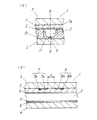
従来のAC型プラズマディスプレイパネルの要部断面図を図6に示す。図6(b)は図6(a)のB−B断面図である。
【0003】
従来のAC型プラズマディスプレイパネル(以下、パネルという)1は、図6に示すように、放電空間2を挟んでガラス製の表面基板3およびガラス製の背面基板4が対向して配置されている。表面基板3上には、誘電体層5および保護膜6で覆われた対を成す帯状の走査電極7と維持電極8とからなる電極群が互いに平行配列されている。走査電極7および維持電極8はそれぞれ、透明電極7a、8aと導電性を高めるための金属母線7b、8bとから構成されている。
【0004】
背面基板4上には、走査電極7および維持電極8と直交する方向に帯状のデータ電極9が互いに平行配列されており、またこの各データ電極9を隔離し、かつ放電空間2を形成するための帯状の隔壁10がデータ電極9の間に設けられている。また、データ電極9上から隔壁10の側面にわたって蛍光体11が形成されている。さらに、放電空間2にはヘリウム(He)、ネオン(Ne)およびアルゴン(Ar)のうち少なくとも一種とキセノン(Xe)との混合ガスが封入されている。
【0005】
このパネル1は表面基板3側から画像表示を見るようになっており、放電空間2内での走査電極7と維持電極8との間の放電により発生する紫外線によって、蛍光体11を励起し、この蛍光体11からの可視光を表示発光に利用するものである。
【0006】
次に、従来のパネル1に画像データを表示させる方法について説明する。
【0007】
従来のパネルを駆動する方法として、1フィールド期間を2進法に基づいた発光期間の重みを持った複数のサブフィールドに分割し、発光させるサブフィールドの組み合わせによって階調表示を行う。各サブフィールドは初期化期間、アドレス期間および維持期間からなる。
【0008】
画像データを表示するためには、初期化期間、アドレス期間および維持期間でそれぞれ異なる信号波形を各電極に印加する。初期化期間には、たとえば、維持電極8およびデータ電極9に対して正極性のパルス電圧をすべての走査電極7に印加し、保護膜6および蛍光体11上に壁電荷を蓄積する。
【0009】
アドレス期間では、すべての走査電極7に順次、負極性のパルスを印加することにより走査していく。表示データがある場合、走査電極7を走査している間に、データ電極9に正極性のデータパルスを印加すると、走査電極7とデータ電極9との間で放電が起こり、走査電極7上の保護膜6の表面に壁電荷が形成される。
【0010】
続く維持期間では一定の期間、走査電極7と維持電極8との間に放電を維持するのに十分な電圧を印加する。これにより、走査電極7と維持電極8との間に放電プラズマが生成され、一定の期間、蛍光体11を励起発光させる。アドレス期間においてデータパルスが印加されなかった放電空間では、放電は発生せず蛍光体11の励起発光は起こらない。
【0011】
このような従来のパネル1では、走査電極7と維持電極8との距離(電極間距離)dは、パッシェンの法則で決まる最小放電電圧が得られる値の近くに設定されている。これは、維持期間において走査電極7と維持電極8との間に印加する外部維持電圧VSUSを低くするためである。すなわち、走査電極7と維持電極8との間の放電開始電圧をVfSSとし、走査電極7上の誘電体層5の壁電圧と維持電極8上の誘電体層5の壁電圧との和をVwSSとするとき、放電空間に加わる電圧はVSUS+VwSSであるため、走査電極7と維持電極8との間で放電を維持するためには、
VfSS<VSUS+VwSS (1)
でなければならない。VfSSが最小になるようにパネルを設計することで、より低い外部維持電圧VSUSで放電を維持することができる。外部維持電圧VSUSは低いほど回路設計が容易になり、また無効電力による損失も低減できる。
【0012】
現在、製造されているパネルでは、封入ガスの全圧が約50〜60kPa、電極間距離dが80〜100μmにおいてVSUSは極小となり、VSUS=180〜200Vを得ている。またその場合、キセノンガスの分圧が5〜10%で、最も発光効率が高くなることが知られている。
【0013】
【発明が解決しようとする課題】
しかし従来のパネルでは、CRTなどの表示装置と比較して発光効率が著しく低いという課題があった。たとえば上述した、電極間距離dが80〜100μmのパネルでは、発光効率は1lm/W前後とCRTの5分の1程度である。
【0014】
また、一般に放電を起こす電極間の距離を長くすると発光効率は上昇することが知られているが、走査電極7と維持電極8との距離を長くすると放電開始電圧VfSSもパッシェン曲線にしたがって急激に上昇し、駆動が困難になるという課題があった。
【0015】
本発明はこのような課題を解決するためになされたもので、電極間距離を長くした場合においても、放電維持のための印加電圧を大きく上昇させることなく、発光効率の高いAC型プラズマディスプレイ装置を提供することを目的とする。
【0016】
【課題を解決するための手段】
本発明のAC型プラズマディスプレイ装置は、第1の誘電体層で覆われた第1電極および第2電極が互いに平行に形成された基板と、第2の誘電体層で覆われた第3電極が前記第1電極と直交する方向に形成された別の基板とが放電空間を挟んで対向配置され、前記第1電極と前記第2電極との距離が、前記第3電極の中心線上における前記放電空間の高さよりも大きく設定されており、維持期間において、前記第1電極および前記第2電極に交互に維持パルス電圧を印加し、前記第1電極または前記第2電極と前記第3電極との間で放電を起こすことにより、前記第1電極と前記第2電極との間に放電を誘発させるものである。
【0017】
この構成により、放電維持電圧を大きく上昇させることなく、維持放電が発生する電極間距離を大きくすることができ、発光効率が大幅に向上したAC型プラズマディスプレイ装置を得ることができる。
【0018】
【発明の実施の形態】
以下、本発明の一実施の形態について図面を用いて説明する。
【0019】
本発明の第1の実施形態のAC型プラズマディスプレイパネル(以下、パネルという)の要部断面図を図1に示す。図1(b)は図1(a)のC−C断面図である。
【0020】
図1に示すように、本発明の第1の実施形態のパネル12は、放電空間2を挟んでガラス製の表面基板3とガラス製の背面基板4とが対向して配置されている。表面基板3上には、誘電体層5および保護膜6からなる第1の誘電体層で覆われた帯状の第1電極Xと第2電極Yとからなる電極対が複数配列されている。保護膜6として酸化マグネシウム(MgO)等の二次電子放射係数の高い材料を用いている。
【0021】
背面基板4上には、第1電極Xおよび第2電極Yと直交する方向に、複数の帯状の第3電極Aが配列されており、この各第3電極Aを隔離し、かつ放電空間2を形成するための帯状の隔壁10が第3電極Aの間に設けられている。また、第3電極A上から隔壁10の側面にわたって第2の誘電体層である蛍光体11が形成されている。さらに、放電空間2にはHe、Ne、Arのうち、少なくとも一種とXeとの混合ガスが封入されている。1つの第1電極Xおよび第2電極Yと1つの第3電極Aとの交差部に1つの放電セルが構成される。そして、赤色、緑色および青色の蛍光体がそれぞれ形成され、互いに隣接した3つの放電セルにより、1つの画素を構成している。
【0022】
このパネル12は表示面側である表面基板3側から画像表示を見るようになっており、放電空間2内の放電により発生する紫外線によって、蛍光体11を励起し、この蛍光体11から発生する可視光を表示発光に利用するものである。
【0023】
本実施形態のパネルにおいては、第1電極Xと第2電極Yとの距離(以下、維持放電ギャップという)をdSSとし、第3電極Aの中心線上における蛍光体11の表面と保護膜6の表面との距離、すなわち第3電極Aの中心線上における放電空間2の高さ(以下、アドレス放電ギャップという)をdSAとしたとき、dSS>dSAと設定している。また、維持放電空間とは第1電極Xと第2電極Yとの間の放電空間を指すものとし、アドレス放電空間とは第3電極Aと第1電極Xまたは第2電極Yとの間の放電空間を指すものとする。ここで各電極間の放電開始電圧を次のように定義する。
VfSS:第1電極Xと第2電極Yとの間の放電開始電圧
VfSA:第1電極Xを陰極とした場合の第1電極Xと第3電極Aとの間の放電開始電圧、または第2電極Yを陰極とした場合の第2電極Yと第3電極Aとの間の放電開始電圧
VfAS:第3電極Aを陰極とした場合の第1電極Xと第3電極Aとの間の放電開始電圧、または第3電極Aを陰極とした場合の第2電極Yと第3電極Aとの間の放電開始電圧
VfSSA:第1電極Xと第3電極Aとの間、または第2電極Yと第3電極Aとの間に放電が存在している場合の、第1電極Xと第2電極Yとの間の放電開始電圧放電開始電圧VfSSは従来のパネルにおける、走査電極7と維持電極8との間の放電開始電圧と同じものだが、本実施形態では、維持放電ギャップを大きくしているので、従来のパネルにおける走査電極7と維持電極8との間の放電開始電圧より大きな値となる。放電開始電圧VfSAと放電開始電圧VfASとは互いに放電の極性が逆の場合の放電開始電圧であるが、VfSAは二次電子放射係数が高い保護膜6を陰極側としたときの放電開始電圧であるのに対して、VfASは二次電子放射係数が保護膜6と比較してかなり低い蛍光体を陰極側としたときの放電開始電圧であるため、VfSA≪VfASの関係がある。また、第1電極Xと第3電極Aとの間、または第2電極Yと第3電極Aとの間であらかじめ放電が起っていると、その放電が起こっている放電空間には多量の電荷が存在するため、第1電極Xと第2電極Yとの間の放電開始電圧は低下し、VfSSA≪VfSSとなる。
【0024】
次に、本実施形態のパネル12に画像データを表示させる方法について説明する。
【0025】
本実施形態のパネル12を駆動する方法として、1フィールド期間を2進法に基づいた発光期間の重みを持った複数のサブフィールドに分割し、発光させるサブフィールドの組み合わせによって階調表示を行う。各サブフィールドは初期化期間、アドレス期間および維持期間からなる。
【0026】
画像データを表示するためには、初期化期間、アドレス期間および維持期間でそれぞれ異なる信号波形を電極に印加する。初期化期間には、たとえば、第2電極Yおよび第3電極Aに対して正極性のパルス電圧をすべての第1電極Xに印加し、保護膜6および蛍光体11上に壁電荷を蓄積する。アドレス期間では、すべての第1電極Xに順次、負極性のパルスを印加することにより走査していく。表示データがある場合、第1電極Xを走査している間に第3電極Aに正極性のデータパルスを印加すると、第3電極Aと第1電極Xとの間で放電が起こり、第1電極X上の保護膜6表面に壁電荷が形成される。
【0027】
続く維持期間でのパネルの駆動方法について、図2および図3を参照しながら説明する。
【0028】
図2(a)は第1電極Xに印加する電圧波形Vx(t)であり、図2(b)は第2電極Yに印加する電圧波形Vy(t)であり、図2(c)は第3電極Aに印加する電圧波形Va(t)である。Vx(t)およびVy(t)は振幅がVSUS(V)の維持パルス電圧であり、Va(t)は0Vである。
【0029】
図3(a)において、実線は第2電極Yから見た第1電極Xの電圧波形Vx(t)−Vy(t)を表している。また、破線は第1電極Xと第2電極Yとの間の壁電圧を表しており、第1電極X上の誘電体層5に蓄積された壁電圧と第2電極Y上の誘電体層5に蓄積された壁電圧との和である。図3(b)において、実線は第3電極Aから見た第1電極Xの電圧波形Vx(t)−Va(t)を表している。また、破線は第1電極Xと第3電極Aとの間の壁電圧を表しており、第1電極X上の誘電体層5に蓄積された壁電圧と第3電極A上の蛍光体11に蓄積された壁電圧との和である。図3(c)において、実線は第3電極Aから見た第2電極Yの電圧波形Vy(t)−Va(t)を実線で表している。また、破線は、第2電極Yと第3電極Aとの間の壁電圧を表しており、第2電極Y上の誘電体層5に蓄積された壁電圧と第3電極A上の蛍光体11に蓄積された壁電圧との和である。
【0030】
これらの壁電圧はそれぞれの場合に応じて保護膜6または蛍光体11上に蓄積される壁電荷によって生じたものである。壁電圧の極性は、印加電圧と壁電圧との差が、それぞれの電極間の放電空間に加わる電圧を表すように設定されている。
【0031】
ここで、発生した放電によって蓄積される壁電圧の大きさは、外部から印加した電圧とほぼ同じ大きさになるものとしている。すなわち、図3(a)に示すように、時間t1−Δtおよび時間t3−Δtにおける第1電極Xと第2電極Yとの間の壁電圧VwSS(V)は、外部維持電圧VSUS(V)とほぼ同じ大きさとなっている。また、図3(b)および図3(c)に示すように、時間t1−Δtにおける第1電極Xと第3電極Aとの間の壁電圧と時間t3−Δtにおける第2電極Yと第3電極Aとの間の壁電圧とはほぼ同じ大きさの壁電圧VwSA(V)であり、この壁電圧VwSA(V)は外部維持電圧VSUS(V)とほぼ同じ大きさとなっている。ここで、Δtは時間t3−t1に比べて十分小さい時間である。
【0032】
本実施の形態では、パネルを駆動する場合、
VfSA<VwSA<VfAS (2)
VfSSA<VSUS+VwSS<VfSS (3)
の関係を満足するように、外部から印加する外部維持電圧VSUSの値を設定している。ここで、VwSS≒VSUS、VwSA≒VSUSであるので、
VfSA<VSUS<VfAS (4)
VfSSA/2<VSUS<VfSS/2 (5)
である。次に、維持期間におけるパネルの動作について図3を用いて説明する。
【0033】
まず時間t1+Δtにおいて、第1電極Xと第3電極Aとの間の放電空間には、第1電極Xを負極性すなわち陰極として、VwSA(V)の電圧が加わる。したがって、式(2)より、第1電極Xと第3電極Aとの間で放電が開始する。一方、第2電極Yと第3電極Aとの間の放電空間には、第3電極Aを負極性すなわち陰極として約VSUS(V)の電圧が加わる。したがって、式(4)より、第2電極Yと第3電極Aとの間では放電は開始しない。
【0034】
第1電極Xと第3電極Aとの間で放電が開始すると、この放電によって第1電極Xと第2電極Yとの間の放電開始電圧はVfSSA(V)まで低下する。第1電極Xと第2電極Yとの間の放電空間に加わる電圧はVSUS+VwSS(V)であり、式(3)より、第1電極Xと第2電極Yとの間で放電が開始する。その結果、表示発光が起こるとともに、放電空間内の電位を打ち消すように壁電圧が形成されるので、時間t2では第1電極Xと第2電極Yとの間の放電は停止する。
【0035】
次に時間t3において、第1電極Xおよび第2電極Yに印加される電圧の極性が反転する。その結果、第1電極Xと第2電極Yとを入れ替えた形で時間t1から時間t3に至ったのと同様な過程を経て、第1電極Xと第2電極Yとの間に放電が形成され、時間t1から時間t4に至る1周期の維持動作が完了する。
【0036】
以上のような動作を繰り返すことによって、大きな維持放電ギャップdSSを有するパネルについて比較的低い電圧で表示放電を維持することができる。
【0037】
次に、本実施の形態のパネルを駆動する場合の維持期間における印加電圧について、図4を用いて説明する。図4では横軸に維持放電ギャップdSSを、縦軸に電圧をとっている。放電開始電圧VfSSは比較的小さな維持放電ギャップdSSで極小値を持ついわゆるパッシェンの曲線となる。また、放電開始電圧VfSSAは放電開始電圧VfSSとほぼ同形状の曲線となるが、その値は放電開始電圧VfSSよりも低い。一方、放電開始電圧VfASおよび放電開始電圧VfSAは維持放電ギャップdSSに依存せず、ほぼ水平な直線となる。なお、dSS=dSAにおいて必ずしもVfSS=VfSAになるとは限らない。これは、維持放電空間での電界分布とアドレス放電空間での電界分布とが異なるからである。図4に示した例では、dSS=dSAのとき、VfSS>VfSAとした。
【0038】
本実施形態のパネルでは、維持期間において式(4)および式(5)を満たす領域Dで動作させている。これにより、維持放電ギャップdSSをdSS>dSAのように従来例より大きくした場合でも、アドレス放電空間で発生した放電によって維持放電を誘発させることができるため、発光効率が大幅に上昇する。また、維持放電ギャップdSSを大きくしたにもかかわらず、比較的低い外部印加電圧で放電を維持することができる。さらに、VfSSA/2=VfSAとなる維持放電ギャップdSSをd0とするとき、dSS≦d0と設定することにより、外部維持電圧VSUSの最低値を従来のパネルの最大維持電圧(〜VSA)とほぼ同等とすることができるので、駆動回路に大きな負担をかけることなく発光効率を向上することができる。
【0039】
一方、従来のパネルでは、たとえばdSA=130〜150μm、dSS=80〜100μmというように電極間距離の関係がdSS<dSAとなるように設計されていた。このような従来のパネルを駆動する場合の維持期間では、式(1)の条件に加えて、
VwSA<VfSA (6)
となるような外部維持電圧VSUSを印加していた。したがって、維持期間においてVwSS≒VSUS、VwSA≒VSUSとすると、従来のパネルでは、式(1)および式(6)を満たす領域E(図4参照)で動作させており、アドレス放電空間で放電は起こっていなかった。
【0040】
次に、本実施の形態によるパネルの設計パラメータの一例を表1に示す。
【0041】
【表1】

このパネルにおいて、各放電開始電圧は、
VfSS=700V
VfSA=250V
VfAS=350V
VfSSA=450V
であり、VSUS=270V、t3−t1=t4−t3=2.5μsとすることにより、安定したパネル駆動を行うことができた。本実施の形態のパネルでは、維持放電ギャップdSSが400μmのように従来のパネルの維持放電ギャップ(80〜100μm)に比べて4倍程度大きくなっている。このため、従来の駆動方法を用いた場合には、維持電圧が約400V以上と非常に大きくなってしまい、安定した維持放電を行うことができないが、前述のようにアドレス放電空間で発生した放電によって維持放電空間に放電を誘発させることにより、電圧を大幅に上昇させることなく安定した維持放電を行うことができる。また、このパネルでは、約2lm/Wの発光効率を得ることができた。従来のパネルの発光効率は約1lm/Wであるため、本実施の形態のパネルでは、従来のパネルに比べて、発光効率が2倍近く向上した。
【0043】
以上のように本実施の形態においては、維持放電ギャップを大きくすることができるため、発光効率が高く、かつ駆動電圧の上昇を抑制したAC型プラズマディスプレイ装置を得ることができる。
【0044】
次に本発明の第2の実施形態を図5を用いて説明する。
【0045】
図5に示すように、本発明の第2の実施形態のパネルは、図1に示す第1の実施形態のパネルと基本的にほぼ同じ構成である。異なるのは、第1電極Xおよび第2電極Yを、それぞれITO(Indium Tin Oxide)等からなる透明電極Xa、Yaと銀等からなる金属母線Xb、Ybとで構成したことにある。
【0046】
第2の実施形態では、開口率を低下させることなく第1電極Xおよび第2電極Yの幅を広げることができるので、放電電流を大きくとることができ、輝度が向上する。また、一般に透明電極は抵抗値が高いため、金属母線を設けることによって導電性を高めている。
【0047】
このように第2の実施形態においては、発光効率が高く、かつ駆動電圧の上昇を抑制することができるとともに、発光輝度が高いAC型プラズマディスプレイ装置を得ることができる。
【0048】
なお、上記実施の形態ではアドレス期間と維持期間を分離した、いわゆるアドレス−維持分離型駆動を行うAC型プラズマディスプレイパネルについて説明したが、この他のアドレス方法を用いたAC型プラズマディスプレイパネルにおいても同様の効果を得ることができる。また、初期化期間およびアドレス期間における印加電圧波形は本実施の形態と同じである必要はなく、画像データの有無に応じて選択的に壁電荷が形成されるものであればよい。
【0049】
【発明の効果】
以上のように、本発明は、維持放電ギャップがアドレス放電ギャップよりも大きく設定されたAC型プラズマディスプレイパネルにおいて、維持期間に、アドレス放電空間で発生した放電によって維持放電空間に放電を誘発させることにより、維持電圧を大幅に高めることなく発光効率の向上したAC型プラズマディスプレイ装置を提供することができる。
【図面の簡単な説明】
【図1】本発明の第1の実施形態のAC型プラズマディスプレイパネルの要部断面図
【図2】本発明の第1の実施形態のAC型プラズマディスプレイパネルの維持電圧波形を示す図
【図3】本発明の第1の実施形態のAC型プラズマディスプレイパネルの各電極間の電圧波形および壁電圧波形を示す図
【図4】本発明のAC型プラズマディスプレイパネルの維持期間における動作電圧を説明する図
【図5】本発明の第2の実施形態のAC型プラズマディスプレイパネルの要部断面図
【図6】従来のAC型プラズマディスプレイパネルの要部断面図
【符号の説明】
2 放電空間
3 表面基板
4 背面基板
5 誘電体層
6 保護膜
10 隔壁
11 蛍光体
12 パネル
X 第1電極
Y 第2電極
A 第3電極[0001]
BACKGROUND OF THE INVENTION
The present invention relates to an AC type plasma display apparatus.
[0002]
[Prior art]
FIG. 6 shows a cross-sectional view of a main part of a conventional AC type plasma display panel. FIG. 6B is a cross-sectional view taken along the line BB in FIG.
[0003]
As shown in FIG. 6, a conventional AC plasma display panel (hereinafter referred to as “panel”) 1 has a
[0004]
On the
[0005]
The panel 1 is configured to view an image display from the
[0006]
Next, a method for displaying image data on the conventional panel 1 will be described.
[0007]
As a conventional method of driving a panel, one field period is divided into a plurality of subfields having a light emission period weight based on the binary system, and gradation display is performed by a combination of subfields to emit light. Each subfield includes an initialization period, an address period, and a sustain period.
[0008]
In order to display image data, different signal waveforms are applied to each electrode in the initialization period, the address period, and the sustain period. In the initialization period, for example, a positive pulse voltage is applied to all the
[0009]
In the address period, scanning is performed by sequentially applying a negative pulse to all the
[0010]
In the subsequent sustain period, a voltage sufficient to maintain the discharge is applied between
[0011]
In such a conventional panel 1, the distance (interelectrode distance) d between the
Vf SS <V SUS + Vw SS (1)
Must. By designing the panel so that Vf SS is minimized, the discharge can be maintained with a lower external sustain voltage VSUS . The lower the external sustain voltage VSUS, the easier the circuit design, and the loss due to reactive power can be reduced.
[0012]
In the panel currently manufactured, when the total pressure of the sealed gas is about 50 to 60 kPa and the distance d between the electrodes is 80 to 100 μm, V SUS is minimized, and V SUS = 180 to 200 V is obtained. In that case, it is known that the luminous efficiency is highest when the partial pressure of xenon gas is 5 to 10%.
[0013]
[Problems to be solved by the invention]
However, the conventional panel has a problem that the light emission efficiency is significantly lower than that of a display device such as a CRT. For example, in the above-described panel having an interelectrode distance d of 80 to 100 μm, the luminous efficiency is around 1 lm / W, which is about 1/5 of the CRT.
[0014]
In general, it is known that the light emission efficiency increases when the distance between the electrodes that cause discharge is increased. However, when the distance between the
[0015]
The present invention has been made to solve such a problem. Even when the distance between the electrodes is increased, the AC type plasma display device has a high luminous efficiency without greatly increasing the applied voltage for maintaining the discharge. The purpose is to provide.
[0016]
[Means for Solving the Problems]
The AC type plasma display apparatus of the present invention includes a substrate on which a first electrode and a second electrode covered with a first dielectric layer are formed in parallel to each other, and a third electrode covered with a second dielectric layer. Is disposed opposite to another substrate formed in a direction orthogonal to the first electrode across a discharge space, and the distance between the first electrode and the second electrode is the center line on the third electrode. The height of the discharge space is set to be larger, and during the sustain period, a sustain pulse voltage is alternately applied to the first electrode and the second electrode, and the first electrode or the second electrode and the third electrode Is caused to cause a discharge between the first electrode and the second electrode.
[0017]
With this configuration, it is possible to increase the distance between the electrodes where the sustain discharge is generated without greatly increasing the discharge sustain voltage, and it is possible to obtain an AC type plasma display device in which the light emission efficiency is significantly improved.
[0018]
DETAILED DESCRIPTION OF THE INVENTION
Hereinafter, an embodiment of the present invention will be described with reference to the drawings.
[0019]
FIG. 1 shows a cross-sectional view of a main part of an AC type plasma display panel (hereinafter referred to as a panel) according to a first embodiment of the present invention. FIG.1 (b) is CC sectional drawing of Fig.1 (a).
[0020]
As shown in FIG. 1, in the
[0021]
On the
[0022]
The
[0023]
In the panel of the present embodiment, the distance between the first electrode X and the second electrode Y (hereinafter referred to as the sustain discharge gap) is d SS, and the surface of the
Vf SS : discharge start voltage between the first electrode X and the second electrode Y Vf SA : discharge start voltage between the first electrode X and the third electrode A when the first electrode X is used as a cathode, or Discharge starting voltage Vf AS between the second electrode Y and the third electrode A when the second electrode Y is a cathode: between the first electrode X and the third electrode A when the third electrode A is a cathode The discharge start voltage between the first electrode X and the third electrode A, or the discharge start voltage Vf SSA between the second electrode Y and the third electrode A when the third electrode A is the cathode, or When there is a discharge between the second electrode Y and the third electrode A, the discharge start voltage Vf SS between the first electrode X and the second electrode Y is a scan in the conventional panel. Although it is the same as the discharge start voltage between the
[0024]
Next, a method for displaying image data on the
[0025]
As a method of driving the
[0026]
In order to display image data, different signal waveforms are applied to the electrodes in the initialization period, the address period, and the sustain period. In the initialization period, for example, a positive pulse voltage with respect to the second electrode Y and the third electrode A is applied to all the first electrodes X, and wall charges are accumulated on the
[0027]
A method for driving the panel in the subsequent sustain period will be described with reference to FIGS.
[0028]
2A shows a voltage waveform Vx (t) applied to the first electrode X, FIG. 2B shows a voltage waveform Vy (t) applied to the second electrode Y, and FIG. 4 is a voltage waveform Va (t) applied to the third electrode A. Vx (t) and Vy (t) are sustain pulse voltages having an amplitude of V SUS (V), and Va (t) is 0V.
[0029]
In FIG. 3A, the solid line represents the voltage waveform Vx (t) −Vy (t) of the first electrode X viewed from the second electrode Y. A broken line represents a wall voltage between the first electrode X and the second electrode Y, and the wall voltage accumulated in the
[0030]
These wall voltages are generated by wall charges accumulated on the
[0031]
Here, the magnitude of the wall voltage accumulated by the generated discharge is assumed to be substantially the same as the voltage applied from the outside. That is, as shown in FIG. 3A, the wall voltage Vw SS (V) between the first electrode X and the second electrode Y at time t 1 −Δt and time t 3 −Δt is equal to the external sustain voltage V It is almost the same size as SUS (V). Further, as shown in FIGS. 3B and 3C, the wall voltage between the first electrode X and the third electrode A at time t 1 -Δt and the second electrode Y at time t 3 -Δt. The wall voltage between the first electrode A and the third electrode A is a wall voltage Vw SA (V) having substantially the same magnitude, and this wall voltage Vw SA (V) is substantially the same as the external sustain voltage V SUS (V). It has become. Here, Δt is a time sufficiently smaller than time t 3 −t 1 .
[0032]
In the present embodiment, when driving the panel,
Vf SA <Vw SA <Vf AS (2)
Vf SSA <V SUS + Vw SS <Vf SS (3)
The value of the external sustain voltage VSUS applied from the outside is set so as to satisfy the above relationship. Here, since Vw SS ≈V SUS and Vw SA ≈V SUS ,
Vf SA <V SUS <Vf AS (4)
Vf SSA / 2 <V SUS <Vf SS / 2 (5)
It is. Next, operation of the panel in the sustain period will be described with reference to FIG.
[0033]
First, at time t 1 + Δt, a voltage of Vw SA (V) is applied to the discharge space between the first electrode X and the third electrode A with the first electrode X serving as a negative polarity, that is, a cathode. Therefore, the discharge starts between the first electrode X and the third electrode A from Equation (2). On the other hand, a voltage of about V SUS (V) is applied to the discharge space between the second electrode Y and the third electrode A using the third electrode A as a negative polarity, that is, a cathode. Therefore, the discharge does not start between the second electrode Y and the third electrode A from the equation (4).
[0034]
When the discharge starts between the first electrode X and the third electrode A, the discharge start voltage between the first electrode X and the second electrode Y decreases to Vf SSA (V) due to this discharge. The voltage applied to the discharge space between the first electrode X and the second electrode Y is V SUS + Vw SS (V). From the equation (3), the discharge is generated between the first electrode X and the second electrode Y. Start. As a result, the display light emission occurs because the wall voltage is formed so as to cancel a potential in the discharge space, a discharge between the time t 2 and the first electrode X and the second electrode Y is stopped.
[0035]
Next, at time t 3 , the polarity of the voltage applied to the first electrode X and the second electrode Y is reversed. As a result, a discharge is generated between the first electrode X and the second electrode Y through a process similar to that from the time t 1 to the time t 3 with the first electrode X and the second electrode Y interchanged. And the sustain operation for one cycle from time t 1 to time t 4 is completed.
[0036]
By repeating the above operation, it is possible to maintain the display discharge at a relatively low voltage for the panel having a large sustain discharge gap d SS.
[0037]
Next, the applied voltage in the sustain period when driving the panel of this embodiment will be described with reference to FIG. In FIG. 4, the horizontal axis represents the sustain discharge gap d SS and the vertical axis represents the voltage. The discharge start voltage Vf SS is a so-called Paschen curve having a minimum value with a relatively small sustain discharge gap d SS . Further, the discharge start voltage Vf SSA is a curve having substantially the same shape as the discharge start voltage Vf SS , but its value is lower than the discharge start voltage Vf SS . On the other hand, the discharge start voltage Vf AS and the discharge start voltage Vf SA do not depend on the sustain discharge gap d SS and are almost horizontal straight lines. It should be noted that Vf SS = Vf SA is not always satisfied when d SS = d SA . This is because the electric field distribution in the sustain discharge space is different from the electric field distribution in the address discharge space. In the example shown in FIG. 4, when d SS = d SA , Vf SS > Vf SA .
[0038]
In the panel of the present embodiment, the operation is performed in the region D that satisfies the expressions (4) and (5) in the sustain period. As a result, even when the sustain discharge gap d SS is made larger than the conventional example such that d SS > d SA , the sustain discharge can be induced by the discharge generated in the address discharge space, so that the light emission efficiency is significantly increased. . In addition, the discharge can be maintained at a relatively low externally applied voltage even though the sustain discharge gap d SS is increased. Further, when the sustain discharge gap d SS to be Vf SSA / 2 = Vf SA and d 0, by setting d SS ≦ d 0, the maximum sustaining voltage of the conventional panel the minimum value of the external sustain voltage V SUS Since it can be substantially equal to (˜V SA ), the light emission efficiency can be improved without imposing a heavy burden on the drive circuit.
[0039]
On the other hand, the conventional panel is designed so that the relationship between the distances between the electrodes is d SS <d SA , for example, d SA = 130 to 150 μm and d SS = 80 to 100 μm. In the sustain period when driving such a conventional panel, in addition to the condition of equation (1),
Vw SA <Vf SA (6)
An external sustaining voltage VSUS was applied so that Therefore, Vw SS ≒ V SUS in the sustain period, when Vw SA ≒ V SUS, in the conventional panel, and is operated in a region satisfying the equation (1) and (6) E (see FIG. 4), the address discharge There was no discharge in the space.
[0040]
Next, Table 1 shows an example of the design parameters of the panel according to the present embodiment.
[0041]
[Table 1]
In this panel, each discharge start voltage is
Vf SS = 700V
Vf SA = 250V
Vf AS = 350V
Vf SSA = 450V
By setting V SUS = 270 V and t 3 -t 1 = t 4 -t 3 = 2.5 μs, stable panel driving could be performed. In the panel of the present embodiment, the sustain discharge gap d SS is about 4 times larger than the sustain discharge gap (80 to 100 μm) of the conventional panel, such as 400 μm. For this reason, when the conventional driving method is used, the sustain voltage becomes as large as about 400 V or more, and stable sustain discharge cannot be performed. However, the discharge generated in the address discharge space as described above. By inducing a discharge in the sustain discharge space, a stable sustain discharge can be performed without significantly increasing the voltage. Also, with this panel, a luminous efficiency of about 2 lm / W could be obtained. Since the light emission efficiency of the conventional panel is about 1 lm / W, the light emission efficiency of the panel according to the present embodiment is nearly doubled as compared with the conventional panel.
[0043]
As described above, in this embodiment, since the sustain discharge gap can be increased, an AC type plasma display device with high luminous efficiency and suppressed increase in driving voltage can be obtained.
[0044]
Next, a second embodiment of the present invention will be described with reference to FIG.
[0045]
As shown in FIG. 5, the panel of the second embodiment of the present invention has basically the same configuration as the panel of the first embodiment shown in FIG. The difference is that the first electrode X and the second electrode Y are composed of transparent electrodes Xa, Ya made of ITO (Indium Tin Oxide) or the like and metal bus bars Xb, Yb made of silver or the like.
[0046]
In the second embodiment, since the widths of the first electrode X and the second electrode Y can be increased without reducing the aperture ratio, the discharge current can be increased, and the luminance is improved. Moreover, since a transparent electrode generally has a high resistance value, conductivity is enhanced by providing a metal bus bar.
[0047]
As described above, in the second embodiment, it is possible to obtain an AC type plasma display device having high luminous efficiency and suppressing an increase in driving voltage and having high luminous luminance.
[0048]
In the above embodiment, an AC type plasma display panel that performs so-called address-sustain separation type driving in which an address period and a sustain period are separated has been described. However, an AC type plasma display panel using another address method is also applicable. Similar effects can be obtained. The applied voltage waveform in the initialization period and the address period does not have to be the same as that in the present embodiment, and any wall charge may be selectively formed depending on the presence or absence of image data.
[0049]
【The invention's effect】
As described above, according to the present invention, in the AC plasma display panel in which the sustain discharge gap is set larger than the address discharge gap, the discharge is induced in the sustain discharge space by the discharge generated in the address discharge space during the sustain period. Thus, it is possible to provide an AC type plasma display device with improved luminous efficiency without significantly increasing the sustain voltage.
[Brief description of the drawings]
FIG. 1 is a cross-sectional view of a main part of an AC plasma display panel according to a first embodiment of the present invention. FIG. 2 is a diagram showing a sustain voltage waveform of the AC plasma display panel according to the first embodiment of the present invention. 3 is a diagram showing a voltage waveform between each electrode and a wall voltage waveform of the AC type plasma display panel according to the first embodiment of the present invention. FIG. 4 illustrates an operating voltage during a sustain period of the AC type plasma display panel of the present invention. FIG. 5 is a cross-sectional view of main parts of an AC type plasma display panel according to a second embodiment of the present invention. FIG. 6 is a cross-sectional view of main parts of a conventional AC type plasma display panel.
2 discharge
Claims (7)
Priority Applications (1)
| Application Number | Priority Date | Filing Date | Title |
|---|---|---|---|
| JP6279199A JP4048637B2 (en) | 1999-03-10 | 1999-03-10 | AC type plasma display device |
Applications Claiming Priority (1)
| Application Number | Priority Date | Filing Date | Title |
|---|---|---|---|
| JP6279199A JP4048637B2 (en) | 1999-03-10 | 1999-03-10 | AC type plasma display device |
Publications (2)
| Publication Number | Publication Date |
|---|---|
| JP2000260333A JP2000260333A (en) | 2000-09-22 |
| JP4048637B2 true JP4048637B2 (en) | 2008-02-20 |
Family
ID=13210538
Family Applications (1)
| Application Number | Title | Priority Date | Filing Date |
|---|---|---|---|
| JP6279199A Expired - Fee Related JP4048637B2 (en) | 1999-03-10 | 1999-03-10 | AC type plasma display device |
Country Status (1)
| Country | Link |
|---|---|
| JP (1) | JP4048637B2 (en) |
Families Citing this family (3)
| Publication number | Priority date | Publication date | Assignee | Title |
|---|---|---|---|---|
| CN1295733C (en) * | 1999-12-14 | 2007-01-17 | 松下电器产业株式会社 | AC type plasma display panel capable of high definition high brightness image display, and excitation of driving the same |
| FR2820871B1 (en) * | 2001-02-15 | 2003-05-16 | Thomson Plasma | METHOD FOR CONTROLLING A COPLANAR-TYPE PLASMA VISUALIZATION PANEL USING SUFFICIENTLY HIGH FREQUENCY PULSE TRAINS TO OBTAIN DISCHARGE STABILIZATION |
| JP5044877B2 (en) * | 2001-07-30 | 2012-10-10 | パナソニック株式会社 | Plasma display device |
-
1999
- 1999-03-10 JP JP6279199A patent/JP4048637B2/en not_active Expired - Fee Related
Also Published As
| Publication number | Publication date |
|---|---|
| JP2000260333A (en) | 2000-09-22 |
Similar Documents
| Publication | Publication Date | Title |
|---|---|---|
| KR100341313B1 (en) | Plasma Display Panel And Apparatus And Method Of Driving The Same | |
| JP3121247B2 (en) | AC-type plasma display panel and driving method | |
| JP3727868B2 (en) | Plasma display panel and driving method and apparatus thereof | |
| JP2005141257A (en) | Method for driving plasma display panel | |
| JP3725071B2 (en) | Plasma display panel | |
| KR20010077575A (en) | Plasma Display Panel and Method of Driving the same | |
| JP2001093424A (en) | Ac type plasma display panel and drive method of the same | |
| JP3641240B2 (en) | Plasma display panel and driving method thereof | |
| JP3984794B2 (en) | Plasma display panel and driving method thereof | |
| US20030112206A1 (en) | Ac-type plasma display panel capable of high definition and high brightness image display, and a method of driving the same | |
| JP4052756B2 (en) | AC type plasma display device | |
| JP4285040B2 (en) | Plasma display panel | |
| JP4048637B2 (en) | AC type plasma display device | |
| JP4096466B2 (en) | Driving method of AC type plasma display panel | |
| JP4463344B2 (en) | Driving method of AC type plasma display panel | |
| JP5044877B2 (en) | Plasma display device | |
| JP2001282185A (en) | Ac-type plasma display panel and driving method therefor | |
| WO2004086447A1 (en) | Plasma display panel | |
| JP4461718B2 (en) | Plasma display panel | |
| KR100324261B1 (en) | Plasma Display Panel and Method of Driving the same | |
| JPH10302643A (en) | Plasma display panel and its driving method | |
| KR100273195B1 (en) | Plasma display panel and its driving method | |
| KR100351465B1 (en) | Plasma Display Panel and Method Of Driving The Same | |
| KR20010076098A (en) | Plasma display panel and method of driving the same | |
| JP2000311614A (en) | Ac type plasma display device |
Legal Events
| Date | Code | Title | Description |
|---|---|---|---|
| A621 | Written request for application examination |
Free format text: JAPANESE INTERMEDIATE CODE: A621 Effective date: 20060127 |
|
| RD01 | Notification of change of attorney |
Free format text: JAPANESE INTERMEDIATE CODE: A7421 Effective date: 20060214 |
|
| A977 | Report on retrieval |
Free format text: JAPANESE INTERMEDIATE CODE: A971007 Effective date: 20071025 |
|
| TRDD | Decision of grant or rejection written | ||
| A01 | Written decision to grant a patent or to grant a registration (utility model) |
Free format text: JAPANESE INTERMEDIATE CODE: A01 Effective date: 20071106 |
|
| A61 | First payment of annual fees (during grant procedure) |
Free format text: JAPANESE INTERMEDIATE CODE: A61 Effective date: 20071119 |
|
| FPAY | Renewal fee payment (event date is renewal date of database) |
Free format text: PAYMENT UNTIL: 20101207 Year of fee payment: 3 |
|
| LAPS | Cancellation because of no payment of annual fees |