JP4046881B2 - Optical disc and manufacturing method thereof - Google Patents
Optical disc and manufacturing method thereof Download PDFInfo
- Publication number
- JP4046881B2 JP4046881B2 JP02283599A JP2283599A JP4046881B2 JP 4046881 B2 JP4046881 B2 JP 4046881B2 JP 02283599 A JP02283599 A JP 02283599A JP 2283599 A JP2283599 A JP 2283599A JP 4046881 B2 JP4046881 B2 JP 4046881B2
- Authority
- JP
- Japan
- Prior art keywords
- disk substrate
- disk
- mold
- outer diameter
- substrate
- Prior art date
- Legal status (The legal status is an assumption and is not a legal conclusion. Google has not performed a legal analysis and makes no representation as to the accuracy of the status listed.)
- Expired - Fee Related
Links
Images
Landscapes
- Optical Record Carriers And Manufacture Thereof (AREA)
- Manufacturing Optical Record Carriers (AREA)
Description
【0001】
【発明の属する技術分野】
本発明は、貼り合わせ型の光ディスク及びその製造方法に関するものであり、特に、バリによる貼り合わせ不良の改善に関するものである。
【0002】
【従来の技術】
光記録の分野においては、近年、急速に情報信号の高記録密度化が進められており、これに伴って、いわゆるコンパクトディスク(CD)のような単一のディスク基板を用いた単板型光ディスクに代わり、信号面を形成した2枚のディスク基板を貼り合わせた貼り合わせ光ディスクが提案されている。
【0003】
具体的には、上記信号面を形成した2枚のディスク基板のうち一方のディスク基板の信号面側と他方の基板の読み取り面側とが対向するように接着し、片側から読み取り光を照射することにより、これら各ディスク基板の信号面からの情報を読み出し可能とした光ディスクを挙げることができる。
【0004】
上記構成の貼り合わせ光ディスクは、単板型光ディスクとの上位互換を取り易いこと、再生系を簡略化し易いこと等、例えば両面タイプの貼り合わせ光ディスク等と比較して種々のメリットを有する。
【0005】
【発明が解決しようとする課題】
ところで、上記のような片側から各ディスク基板の信号面の情報を読み出し可能とした光ディスクを製造する場合、これまで全く同一条件で作製されたディスク基板同士を貼り合わせるというのが一般的である。
【0006】
しかしながら、この場合、バリによる貼り合わせ不良が頻繁に発生することがわかってきた。光ディスクにおいて、かかる貼り合わせ不良が発生すると、スキューの悪化が問題となる。
【0007】
貼り合わせ不良を解消するためには、上記バリを除去すればよいが、この場合、バリを除去するための2次工程が別途必要になり、工程が煩雑化するという欠点がある。
【0008】
一方、成形条件を工夫してディスク基板成形時になるべくバリが出ないようにすることも考えられる。
【0009】
しかしながら、この場合には、成形バリを少なくするための高精度の金型が必要となること、成形バリを少なくするための成形条件を採用することにより光学特性等を犠牲にせざるを得なくなること、等の不都合が生ずる。
【0010】
本発明は、かかる従来の実情に鑑みて提案されたものであり、バリによる影響を工程の煩雑化や金型の高精度化、光学特性の劣化等を招くことなく抑えることが可能な光ディスクを提供することを目的とし、さらには、その製造方法を提供することを目的とする。
【0011】
【課題を解決するための手段】
上述の目的を達成するために、本発明の光ディスクは、一方の主面が信号面とされるとともに他方の主面が読み取り面とされた一対のディスク基板を有し、一方のディスク基板の信号面側と他方の基板の読み取り面側とが対向するように接着されてなる光ディスクにおいて、上記読み取り面側が接着面とされたディスク基板の外径寸法が、上記信号面側が接着面とされたディスク基板の外径寸法よりも大であることを特徴とする。
【0012】
また、本発明の光ディスクの製造方法は、少なくとも何れか一方にスタンパが装着された固定側金型と可動側金型によりディスク基板の主面を成形するとともに、外周リングによりディスク基板の外周縁を成形する成形装置を用い、外径寸法の異なる2種類のディスク基板を成形し、外径寸法の大きなディスク基板の読み取り面側と外径寸法の小さなディスク基板の信号面側とが対向するように接着することを特徴とする。
【0013】
光ディスク基板を成形する際に、信号面には外方に向かってバリが発生し、読み取り面には厚さ方向のバリが発生する。
【0014】
このようなバリが発生した同一サイズのディスク基板を貼り合わせると、読み取り面側の厚さ方向のバリが信号面に当たり、貼り合わせ不良が発生し、スキューが劣化する。
【0015】
本発明では、読み取り面側が接着面とされたディスク基板の外径寸法が信号面側が接着面とされたディスク基板の外径寸法よりも大とされているので、読み取り面側の厚さ方向のバリが信号面に当たることはなく、貼り合わせ不良やスキューの劣化が解消される。
【0016】
また、バリを除去するための処理工程や、高精度金型等も不要である。
【0017】
【発明の実施の形態】
以下、本発明を適用した光ディスク及びその製造方法について、図面を参照しながら詳細に説明する。
【0018】
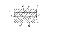
本発明の光ディスクは、例えば図1に示すように、2枚のディスク基板1,2を接着剤層3を介して貼り合わせてなるものである。
【0019】
各ディスク基板1,2は、それぞれ一方の主面が信号面1S,2Sとされるとともに、他方の主面が読み取り光が照射される読み取り面1R,2Rとされている。
【0020】
そして、これらディスク基板1,2は、一方のディスク基板1の信号面1Sに他方のディスク基板2の読み取り面2Rが対向するように貼り合わされている。したがって、ディスク基板1の読み取り面1R側から読み取り光を照射することで、各信号面1S,2Sから信号を読み取ることができる。
【0021】
上記各ディスク基板1,2は、例えばポリカーボネート等のプラスチック材料を射出成形することにより形成されるもので、信号面1S,2Sにはピット、グルーブ等、スタンパの凹凸パターンが転写形成されるとともに、読み取り面1R,2Rは平坦なミラー面とされている。
【0022】
信号面1S,2Sには、反射膜や各種記録膜が形成されるが、特にディスク基板1の信号面1Sには、ディスク基板2の信号面2Sからも信号を読み取る必要があることから、半透過性の反射膜、記録膜を形成することが好ましい。
【0023】
上記構成の貼り合わせ光ディスクにおいて、ディスク基板2の外径寸法D2がディスク基板1の外径寸法D1よりも大とされている。
【0024】
各ディスク基板1,2には、成形の際にバリが生じている。バリとしては、信号面側の外方に向かうバリB1と、読み取り面側の基板厚さ方向のバリB2である。
【0025】
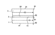
ここで、ディスク基板2の外径寸法D2がディスク基板1の外径寸法D1と同じであると、図2に模式的に示すように、ディスク基板2のバリB2がディスク基板1の信号面1Sに突き当たり、貼り合わせ不良が発生し、スキューが劣化する。
【0026】
これに対して、ディスク基板2の外径寸法D2をディスク基板1の外径寸法D1よりも大とすれば、ディスク基板2のバリB2がディスク基板1の信号面1Sに突き当たることはなく、正常な貼り合わせ状態が維持される。
【0027】
このとき、ディスク基板2の読み取り面2Rのミラー領域がディスク基板1のバリB1部分を含めた信号面よりも大きいことが理想的である。
【0028】
上記ディスク基板2の外径寸法D2をディスク基板1の外径寸法D1よりも0.1mm以上大きくなるように設定すれば、ほぼ確実に前記状態とすることができる。
【0029】
次に、上記光ディスクの製造方法について説明する。
【0030】
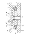
図3は、各ディスク基板を射出成形するための金型構造の一例を示すものである。
【0031】
ディスク基板成形用の金型は、固定金型11と可動金型12とを基本要素とし、これら金型間に形成される空間(キャビティ)内に樹脂を充填することでディスク基板が成形される。
【0032】
固定金型11や可動金型12の内部には、温度調節孔11a,12aが設けられており、射出成形時の金型温度を調節するような構造とされている。
【0033】
固定金型11の中央部には、溶融樹脂が流れ込む流路となるスプルー11bが設けられ、これを中心としてスタンパ13がキャビティに臨んで取り付けられている。
【0034】
なお、上記スタンパ13は、内周スタンパ押さえ14及び外周スタンパ押さえ15により固定金型11に固定されている。
【0035】
一方、上記可動金型12の中央部には、上記スプルー11bと対向してセンターポンチ機構16が設けられており、成形されたディスク基板の突き出し、及びスプルーブッシュの打ち抜きを行うように構成されている。
【0036】
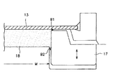
可動金型12は、ディスク基板の読み取り面を形成するためのもので、鏡面状態のミラー面とされているが、その外周には、図4に拡大して示すように、外周リング17が嵌合されている。
【0037】
外周リング17は、ディスク基板の外周形状を決めるものであるが、例えば固定金型11と可動金型12が突き合わされたとき、スタンパ13との間、及び可動金型12のミラー面との間に微少な隙間が生ずる。
【0038】
そして、ディスク基板18の成形時には、この隙間が原因となってバリB1やバリB2が発生する。
【0039】
これらのバリを解消するためには、先ず、高精度な金型を用いることが挙げられるが、この場合には多大な設備投資が必要となる。また、そのメンテナンスも煩雑である。
【0040】
バリを解消するための別の手法としては、射出成形条件の変更等も考えられるが、この場合には成形されるディスク基板の光学特性等を犠牲にせざるを得ず、問題が多い。
【0041】
そこで、本発明では、2枚のディスク基板を成形する際の金型のサイズに若干変更を加え、上記バリの問題に対応することとする。
【0042】
具体的には、読み取り面側が接着されるディスク基板を成形するための金型構造における可動金型12のミラー面の外形寸法Mを、信号面側が接着されるディスク基板を成形するための金型構造における外周リング17の内径φよりも望ましくは0.1mm以上大きくする。
【0043】
すなわち、読み取り面側が接着されるディスク基板と信号面側が接着されるディスク基板を成形するに際し、外周リングの内径及びこれに伴って可動金型のミラー面の外形寸法を変えて成形を行い、外径寸法の異なる2種類のディスク基板として作製する。
【0044】
そして、これらディスク基板を図1に示すように貼り合わせ、貼り合わせ型の光ディスクを完成する。
【0045】
かかる手法を採用することにより、バリを除去するための特別な除去工程を経ることなく正常な貼り合わせ状態を得ることができる。また、高精度な金型や射出条件の変更も不要である。
【0046】
【発明の効果】
以上の説明からも明らかなように、本発明によれば、バリによる影響を工程の煩雑化や金型の高精度化、光学特性の劣化等を招くことなく抑えることが可能である。
【0047】
したがって、スキューの劣化のない、信頼性の高い貼り合わせ型光ディスクを提供することが可能である。
【図面の簡単な説明】
【図1】本発明を適用した貼り合わせ型光ディスクの一構成例を示す要部概略断面図である。
【図2】バリによる貼り合わせ不良の様子を示す模式図である。
【図3】ディスク基板を成形するための金型構造の一例を示す概略断面図である。
【図4】外周リング近傍を拡大して示す要部概略断面図である。
【符号の説明】
1,2 ディスク基板、1S,2S 信号面、1R,2R 読み取り面[0001]
BACKGROUND OF THE INVENTION
The present invention relates to a bonded optical disk and a method for manufacturing the same, and particularly to improvement of bonding failure due to burrs.
[0002]
[Prior art]
In recent years, in the field of optical recording, the recording density of information signals has been rapidly increased. Along with this, a single-plate type optical disk using a single disk substrate such as a so-called compact disk (CD). Instead, a bonded optical disk is proposed in which two disk substrates on which signal surfaces are formed are bonded together.
[0003]
Specifically, of the two disk substrates on which the signal surface is formed, the signal surface side of one disk substrate and the reading surface side of the other substrate are opposed to each other, and the reading light is irradiated from one side. Thus, it is possible to list optical disks that can read information from the signal surfaces of these disk substrates.
[0004]
The bonded optical disk having the above-described configuration has various advantages compared to, for example, a double-sided bonded optical disk and the like, such as easy upward compatibility with a single-plate optical disk and easy reproduction system.
[0005]
[Problems to be solved by the invention]
By the way, when manufacturing an optical disc in which the information on the signal surface of each disc substrate can be read from one side as described above, it is common to bond disc substrates manufactured so far under exactly the same conditions.
[0006]
However, in this case, it has been found that poor bonding due to burrs frequently occurs. When such a bonding failure occurs in an optical disk, deterioration of skew becomes a problem.
[0007]
In order to eliminate the bonding failure, the burrs may be removed. In this case, however, a secondary process for removing the burrs is separately required, and there is a disadvantage that the process becomes complicated.
[0008]
On the other hand, it is conceivable to devise molding conditions so that burrs are not generated as much as possible when the disk substrate is molded.
[0009]
However, in this case, a high-precision mold for reducing molding burrs is required, and optical characteristics and the like must be sacrificed by adopting molding conditions for reducing molding burrs. , Etc. will occur.
[0010]
The present invention has been proposed in view of such a conventional situation, and an optical disc capable of suppressing the influence of burrs without incurring complicated processes, high accuracy of a mold, deterioration of optical characteristics, and the like. It aims at providing, Furthermore, it aims at providing the manufacturing method.
[0011]
[Means for Solving the Problems]
In order to achieve the above-described object, the optical disk of the present invention has a pair of disk substrates in which one main surface is a signal surface and the other main surface is a reading surface, and the signal of one disk substrate is In an optical disk that is bonded so that the surface side and the reading surface side of the other substrate face each other, the outer diameter of the disk substrate having the reading surface side as the bonding surface is the same as the disk having the signal surface side as the bonding surface. It is characterized by being larger than the outer diameter dimension of the substrate.
[0012]
In addition, the optical disk manufacturing method of the present invention forms the main surface of the disk substrate with a fixed mold and a movable mold with a stamper attached to at least one of them, and the outer peripheral edge of the disk substrate with an outer ring. Two types of disk substrates with different outer diameters are formed using a molding device, and the reading surface side of the disk substrate having a larger outer diameter size is opposed to the signal surface side of the disk substrate having a smaller outer diameter size. It is characterized by bonding.
[0013]
When the optical disk substrate is molded, burrs are generated outwardly on the signal surface, and burrs in the thickness direction are generated on the reading surface.
[0014]
When disc substrates of the same size with such burrs are bonded together, the burrs in the thickness direction on the reading surface side hit the signal surface, resulting in poor bonding and degraded skew.
[0015]
In the present invention, the outer diameter dimension of the disk substrate whose reading surface side is the bonding surface is larger than the outer diameter dimension of the disk substrate whose signal surface side is the bonding surface. The burr does not hit the signal surface, and the bonding failure and the skew deterioration are eliminated.
[0016]
Further, there is no need for a processing step for removing burrs or a high-precision mold.
[0017]
DETAILED DESCRIPTION OF THE INVENTION
Hereinafter, an optical disk to which the present invention is applied and a manufacturing method thereof will be described in detail with reference to the drawings.
[0018]
The optical disk of the present invention is formed by bonding two
[0019]
Each of the
[0020]
The
[0021]
Each of the
[0022]
Reflective films and various recording films are formed on the signal surfaces 1S and 2S. In particular, the signal surface 1S of the
[0023]
In the bonded optical disk having the above configuration, the outer diameter D2 of the
[0024]
The
[0025]
Here, if the outer diameter D2 of the
[0026]
On the other hand, if the outer diameter D2 of the
[0027]
At this time, it is ideal that the mirror area of the
[0028]
If the outer diameter D2 of the
[0029]
Next, a method for manufacturing the optical disc will be described.
[0030]
FIG. 3 shows an example of a mold structure for injection molding each disk substrate.
[0031]
A mold for forming a disk substrate has a fixed
[0032]
Inside the fixed
[0033]
A
[0034]
The
[0035]
On the other hand, a
[0036]
The
[0037]
The outer
[0038]
When the
[0039]
In order to eliminate these burrs, first, it is possible to use a high-precision mold. In this case, however, a great investment in equipment is required. Moreover, the maintenance is also complicated.
[0040]
As another method for eliminating the burrs, a change in injection molding conditions and the like can be considered. However, in this case, the optical characteristics of the disk substrate to be molded must be sacrificed and there are many problems.
[0041]
Therefore, in the present invention, the size of the mold when molding two disc substrates is slightly changed to deal with the above-mentioned burr problem.
[0042]
Specifically, the outer dimension M of the mirror surface of the
[0043]
That is, when molding a disk substrate to which the reading surface side is bonded and a disk substrate to which the signal surface side is bonded, molding is performed by changing the inner diameter of the outer ring and the outer dimension of the mirror surface of the movable mold. Two types of disk substrates having different diameters are manufactured.
[0044]
Then, these disk substrates are bonded together as shown in FIG. 1 to complete a bonded optical disk.
[0045]
By adopting such a method, a normal bonded state can be obtained without going through a special removal process for removing burrs. In addition, it is not necessary to change a highly accurate mold and injection conditions.
[0046]
【The invention's effect】
As is clear from the above description, according to the present invention, it is possible to suppress the influence of burrs without incurring complicated processes, high-precision molds, and deterioration of optical characteristics.
[0047]
Accordingly, it is possible to provide a highly reliable bonded optical disk without skew deterioration.
[Brief description of the drawings]
FIG. 1 is a schematic cross-sectional view of an essential part showing a configuration example of a bonded optical disk to which the present invention is applied.
FIG. 2 is a schematic diagram showing a state of bonding failure due to burrs.
FIG. 3 is a schematic cross-sectional view showing an example of a mold structure for molding a disk substrate.
FIG. 4 is an enlarged schematic cross-sectional view of the main part showing the vicinity of an outer peripheral ring.
[Explanation of symbols]
1, 2 Disc substrate, 1S, 2S signal surface, 1R, 2R reading surface
Claims (4)
上記読み取り面側が接着面とされたディスク基板の外径寸法が、上記信号面側が接着面とされたディスク基板の外径寸法よりも大であることを特徴とする光ディスク。It has a pair of disk substrates in which one main surface is a signal surface and the other main surface is a reading surface, so that the signal surface side of one disk substrate faces the reading surface side of the other substrate. In an optical disc bonded to
An optical disc characterized in that the outer diameter of the disk substrate having the reading surface as an adhesive surface is larger than the outer diameter of the disk substrate having the signal surface as an adhesive surface.
外径寸法の大きなディスク基板の読み取り面側と外径寸法の小さなディスク基板の信号面側とが対向するように接着することを特徴とする光ディスクの製造方法。Using a molding apparatus that molds the main surface of the disk substrate with a fixed mold and a movable mold with a stamper attached to at least one of them, and molds the outer peripheral edge of the disk substrate with an outer ring. Mold two different types of disk substrates,
A method of manufacturing an optical disc, comprising: bonding a reading surface side of a disk substrate having a large outer diameter size and a signal surface side of a disk substrate having a small outer diameter size to face each other.
Priority Applications (1)
| Application Number | Priority Date | Filing Date | Title |
|---|---|---|---|
| JP02283599A JP4046881B2 (en) | 1999-01-29 | 1999-01-29 | Optical disc and manufacturing method thereof |
Applications Claiming Priority (1)
| Application Number | Priority Date | Filing Date | Title |
|---|---|---|---|
| JP02283599A JP4046881B2 (en) | 1999-01-29 | 1999-01-29 | Optical disc and manufacturing method thereof |
Publications (2)
| Publication Number | Publication Date |
|---|---|
| JP2000222779A JP2000222779A (en) | 2000-08-11 |
| JP4046881B2 true JP4046881B2 (en) | 2008-02-13 |
Family
ID=12093775
Family Applications (1)
| Application Number | Title | Priority Date | Filing Date |
|---|---|---|---|
| JP02283599A Expired - Fee Related JP4046881B2 (en) | 1999-01-29 | 1999-01-29 | Optical disc and manufacturing method thereof |
Country Status (1)
| Country | Link |
|---|---|
| JP (1) | JP4046881B2 (en) |
-
1999
- 1999-01-29 JP JP02283599A patent/JP4046881B2/en not_active Expired - Fee Related
Also Published As
| Publication number | Publication date |
|---|---|
| JP2000222779A (en) | 2000-08-11 |
Similar Documents
| Publication | Publication Date | Title |
|---|---|---|
| US20050022224A1 (en) | Stamper for manufacturing optical recording medium, method for forming information recording area and light transmitting layer, and optical recording medium | |
| JP2002240101A (en) | Disk substrate, mold apparatus for injection molding the same, and robot for removing the disk substrate | |
| JP4046881B2 (en) | Optical disc and manufacturing method thereof | |
| JP4215923B2 (en) | Optical disc and mold for injection compression molding thereof | |
| US5851620A (en) | Disc metal mold and recorded disc | |
| JP2000298879A (en) | Optical recording medium | |
| JP4769654B2 (en) | Blu-ray Disc manufacturing method | |
| JP4093686B2 (en) | Disc substrate molding die and molding apparatus | |
| JP2005267738A (en) | Metal mold device for forming optical disk substrate | |
| JP2000263615A (en) | Mold for optical information recording medium substrate | |
| JP4306093B2 (en) | Optical recording medium, method for manufacturing the same, and injection molding apparatus | |
| JP2003242680A (en) | Disk-shaped optical recording medium | |
| JP4079541B2 (en) | Disc board | |
| JP4098592B2 (en) | Optical recording medium, molding die for optical recording medium, and substrate for optical recording medium | |
| JP4167422B2 (en) | Mold apparatus for manufacturing disk-shaped substrate material and method for manufacturing disk-shaped substrate material | |
| JP2000094480A (en) | Mold and injection molding machine for disk-shaped recording media | |
| JP3383387B2 (en) | Optical disc substrate and mold for molding this optical disc substrate | |
| JP2002237105A (en) | Intermediate substrate for optical information medium, optical information medium, and manufacturing method of optical information medium | |
| KR20040078667A (en) | Method for manufacturing discoid optical record medium and discoid optical record medium | |
| JP3451842B2 (en) | optical disk | |
| JP2001047471A (en) | Disk substrate molding apparatus and disk-shaped recording medium | |
| JP2003048234A (en) | Optical disk molding die and substrate, and optical disk | |
| JP4109216B2 (en) | Information recording medium | |
| JP2002222545A (en) | Optical disk substrate | |
| JP2006031753A (en) | Disk substrate, optical recording medium and mold apparatus |
Legal Events
| Date | Code | Title | Description |
|---|---|---|---|
| A621 | Written request for application examination |
Free format text: JAPANESE INTERMEDIATE CODE: A621 Effective date: 20051206 |
|
| A977 | Report on retrieval |
Free format text: JAPANESE INTERMEDIATE CODE: A971007 Effective date: 20071015 |
|
| TRDD | Decision of grant or rejection written | ||
| A01 | Written decision to grant a patent or to grant a registration (utility model) |
Free format text: JAPANESE INTERMEDIATE CODE: A01 Effective date: 20071023 |
|
| A61 | First payment of annual fees (during grant procedure) |
Free format text: JAPANESE INTERMEDIATE CODE: A61 Effective date: 20071121 |
|
| FPAY | Renewal fee payment (event date is renewal date of database) |
Free format text: PAYMENT UNTIL: 20101130 Year of fee payment: 3 |
|
| R150 | Certificate of patent or registration of utility model |
Free format text: JAPANESE INTERMEDIATE CODE: R150 |
|
| FPAY | Renewal fee payment (event date is renewal date of database) |
Free format text: PAYMENT UNTIL: 20111130 Year of fee payment: 4 |
|
| FPAY | Renewal fee payment (event date is renewal date of database) |
Free format text: PAYMENT UNTIL: 20111130 Year of fee payment: 4 |
|
| S533 | Written request for registration of change of name |
Free format text: JAPANESE INTERMEDIATE CODE: R313533 |
|
| FPAY | Renewal fee payment (event date is renewal date of database) |
Free format text: PAYMENT UNTIL: 20111130 Year of fee payment: 4 |
|
| R360 | Written notification for declining of transfer of rights |
Free format text: JAPANESE INTERMEDIATE CODE: R360 |
|
| FPAY | Renewal fee payment (event date is renewal date of database) |
Free format text: PAYMENT UNTIL: 20111130 Year of fee payment: 4 |
|
| R360 | Written notification for declining of transfer of rights |
Free format text: JAPANESE INTERMEDIATE CODE: R360 |
|
| R371 | Transfer withdrawn |
Free format text: JAPANESE INTERMEDIATE CODE: R371 |
|
| FPAY | Renewal fee payment (event date is renewal date of database) |
Free format text: PAYMENT UNTIL: 20111130 Year of fee payment: 4 |
|
| S533 | Written request for registration of change of name |
Free format text: JAPANESE INTERMEDIATE CODE: R313533 |
|
| FPAY | Renewal fee payment (event date is renewal date of database) |
Free format text: PAYMENT UNTIL: 20111130 Year of fee payment: 4 |
|
| R350 | Written notification of registration of transfer |
Free format text: JAPANESE INTERMEDIATE CODE: R350 |
|
| FPAY | Renewal fee payment (event date is renewal date of database) |
Free format text: PAYMENT UNTIL: 20111130 Year of fee payment: 4 |
|
| FPAY | Renewal fee payment (event date is renewal date of database) |
Free format text: PAYMENT UNTIL: 20121130 Year of fee payment: 5 |
|
| FPAY | Renewal fee payment (event date is renewal date of database) |
Free format text: PAYMENT UNTIL: 20131130 Year of fee payment: 6 |
|
| LAPS | Cancellation because of no payment of annual fees |