JP4044983B2 - EMC testing equipment for electrical equipment - Google Patents
EMC testing equipment for electrical equipment Download PDFInfo
- Publication number
- JP4044983B2 JP4044983B2 JP34888196A JP34888196A JP4044983B2 JP 4044983 B2 JP4044983 B2 JP 4044983B2 JP 34888196 A JP34888196 A JP 34888196A JP 34888196 A JP34888196 A JP 34888196A JP 4044983 B2 JP4044983 B2 JP 4044983B2
- Authority
- JP
- Japan
- Prior art keywords
- chamber
- conductor
- impedance
- chamber wall
- wire
- Prior art date
- Legal status (The legal status is an assumption and is not a legal conclusion. Google has not performed a legal analysis and makes no representation as to the accuracy of the status listed.)
- Expired - Lifetime
Links
Images


Classifications
-
- G—PHYSICS
- G01—MEASURING; TESTING
- G01R—MEASURING ELECTRIC VARIABLES; MEASURING MAGNETIC VARIABLES
- G01R31/00—Arrangements for testing electric properties; Arrangements for locating electric faults; Arrangements for electrical testing characterised by what is being tested not provided for elsewhere
- G01R31/001—Measuring interference from external sources to, or emission from, the device under test, e.g. EMC, EMI, EMP or ESD testing
Landscapes
- Physics & Mathematics (AREA)
- Electromagnetism (AREA)
- General Physics & Mathematics (AREA)
- Testing Electric Properties And Detecting Electric Faults (AREA)
- Shielding Devices Or Components To Electric Or Magnetic Fields (AREA)
- Tests Of Electronic Circuits (AREA)
- Trip Switchboards (AREA)
- Measurement Of Resistance Or Impedance (AREA)
Description
【0001】
【発明の属する技術分野】
本発明は、導体材料のチャンバーと高周波電源から給電されるチャンバー内に高周波電磁界を発生させる手段とを設けた電気装置の電磁適合性試験(EMC)のための装置に向けられ、且つそれから発展したものである。
【0002】
【従来技術】
EMC(エレクトロマグネティック・コンパチビリティ,電磁適合性)またはEMI(エレクトロマグネティック・インタフィアレンス,電磁界干渉、電磁妨害雑音)測定に対するこの種の装置は既知である。既知の装置中では、チャンバー中の電磁界はもっぱら非対称的励磁システムにより発生される。そのシステムでは金属性のチャンバーが1つの同軸線路システムの外側導体を形成し、チャンバー中に絶縁して保持される金属板が同軸線路の内側導体を形成し、その同軸線路には高周波波電源から非対称的に給電がなされる。(例えばDE 39 31 449, DE 31 30 487, DE 39 25 247, DE37 31 165, DE 43 00 778, EP 0 517 992; ブンデルリッヒ,ベルネル (Wunderlich, Werner)の比較的大形の無線伝送装置の妨害耐性測定、RFZ技術報告、28巻、1号、1984年、220ページ以下;エム.エル.クロウフォード(M. L. Crawford),ジェイ.エル.ワークマン(J. L. Workman),シー.エル.トーマス(C. L. Thomas)の「吸収体装荷大形TEMセルを用いた電磁感受率測定用電界の発生」、IEEE トランズアクションズ・オン・インストルメンテイション・アンド・メジュアメント(IEEE計装測定紀要)の1977年9月、3号、225ページ以降等参照)。
【0003】
これによって、EMC基準によって要求されるチャンバー内での均一な電界強度分布(基準ではテストチャンバー内の電界強度分布の変動が6dB以下であることを要求している)を得るために、被試験物が置かれている内側導体板はできる限りチャンバー中央部に配置されなければならない。しかし、その結果、チャンバー内の空間の半分だけが被試験物の受け入れに利用できるに過ぎない。その上、基準に適合するEMC試験装置は、同軸給電ケーブルから電界を発生するための内側導体線と外側導体線からなるシステムへの遷移部としてのピラミッド形のチャンバー形状を必要とする。したがって非常にかさばったものとなる。
【0004】
これまでに、内側導体を四角いチャンバーの底面壁にできるだけ近く配置することが試みられてきた(例えば英国サーモ・ボルテック(Thermo Voltek)社のGストリップセル形コムテスト)。それによれば、被試験物受け入れのための利用可能空間は、実際、拡大されたが、この既知のセルはチャンバー内の均一電界分布に対する厳密な基準には適合していない。
したがって本発明の1つの目的は、EMC試験装置を創出することである。この目的とは、与えられた最小の空間的な要求で可能な最大の利用可能試験用空間を提供し、しかも厳密な基準によって要求されるチャンバー内に均一電界強度分布を確保することである。前記の目的は、導体材料のチャンバーと、高周波電源から給電された高周波電磁界をチャンバー内に発生させる発生手段と、を設けた電気試験装置から出発し、チャンバーの対向する両側面間に、配置された少なくとも2本の導体線を特徴とし、前記少なくとも2本の導体線は、チャンバーの前記両側面のうちの一つの側面を形成する一つのチャンバー壁から間隔をあけて且つ一つのチャンバー壁と平行になるように配置された少なくとも1本の導体線と、チャンバーの前記両側面のうちの他の側面を形成する他のチャンバー壁から間隔をあけて且つ他のチャンバー壁と平行になるように配置された少なくとも1本の導体線と、を含み、一つの対称型の二線式の線路を形成し、その1端において高周波電源から発生手段によって逆相に給電され、他端において終端インピーダンスを介してチャンバー壁に電気的に接続されていることを特徴とする構造により達成される。諸々の効果は各従属請求項で展開される。
【0005】
本発明の装置においては、チャンバー内の電磁界は、大地(チャンバー容器)に対して対称的に給電される二線式の線路(レッヘル線)によって発生され、一方では、その給電線の導体線はチャンバーの高さによって決まる比較的大きな相互間隔で配置されているが、しかしそれぞれに隣接するチャンバー壁から比較的小さな距離に保たれている。チャンバーの向い合う壁が近いために、電磁界は二線式の線路の外側に、すなわち、導線とチャンバー壁の間に形成される。このような、各導線と隣接する金属チャンバー壁との間に形成される線路システムは、非対称解放形ストリップ線路(マイクロストリップ)と見ることができる。このストリップ線路システムについての特性インピーダンスはそれぞれ、寸法則(導体線のチャンバー壁からの距離、導体線の直径、あるいは、それぞれ導体線の幅、存在するとすれば、導体線とチャンバー壁間に存在する誘電体の幅、などで決まるもの)として知られる方法で計算することができる。そして、導体線とチャンバー壁との間の終端インピーダンスの値もまたこれによって決めることができる。このように大きな空間である結果、給電用として、比較的高いインピーダンスの二線式の線路システムが用いられる。
【0006】
導体線とチャンバー壁との間の空間には電界強度が集中するが、これはEMC測定には利用されず、二線式の線路システムの対向して備わる2本の導体線間の空間に存在する電磁界のみが基準にしたがって要求される試験用の均一分布を伴って利用可能である。1つの実施例では、チャンバー全体での電磁界の変動は±3dBに抑えられている。それにもかかわらず、チャンバーのほとんど全内側空間が被試験物受け入れ用に利用可能であり、したがって、本発明の装置は最小の外側全体寸法で製作可能となる。
【0007】
最も簡単な場合には、二線式の線路システムは互いに対向して置かれたただ2本の導体線だけで形成されるが、本発明での展開にしたがえば、順次隣接配置した複数の導体線を備え、それぞれをチャンバーの一側端から同相で給電することにより、チャンバー壁全面にわたって均一な電界分布を確保することも得策であることがわかってきている。これら次々に配置された個々の導体線は、互いに平行に配置されるのが好ましいが、それは、必ずしも平行配置のみに限ったものではなく、1つの中心となる給電点から発して、チャンバー壁にわたって扇状に分布させてもよい。
【0008】
次々に配置された複数の導体線が与えられると、各々は別の一つの終端インピーダンスを経て大地(チャンバー壁)に終端される。これらの二線式の線路の終端インピーダンスすべての和は、ストリップ線路システムの特性インピーダンスに対応する。このようにして、二線式の線路は、もはや、標準的な二線式の線路が自由空間において形成するであろう比較的高いインピーダンスの特性インピーダンスを持つことがなく、ストリップ線路システムとしてのかなり低い特性インピーダンスを持つことになる。こうして、より有利なことに、入力側から見て低インピーダンス給電についても可能となる。次々に配置された各導体線の終端インピーダンスの寸法を変えることによって、所望の特別なチャンバー内電界分布を発生することも可能である。たとえば、こうしてそこでの終端インピーダンスの対応する寸法を選ぶことにより、チャンバーの各コーナー部での電界分布を最適化することなどが可能である。同じことが、導体線のグループごとに導体線間の個々の間隔を変えて設定することによっても可能である。これらのことを順次隣接して配置された個々の導体線についてそれぞれ別々の終端インピーダンスについて行う代わりに、入力側での給電の場合のように、同じ長さの線路を通して、終端側での1点でまとめて行い、それにより共通の終端インピーダンスを経て大地に接続することもできる。
【0009】
擾乱性の反射を防止するために、特に高周波領域では、適当な高周波吸収体をチャンバーの内壁に付加的にたとえばその間に二線式の線路の導体線が配置されている両端面壁の上に、取り付けることもできる。
一般的に、均一な電界分布を得るのに、チャンバーの互いに対面する2つ内壁間に二線式の線路の導体線を配置するだけで十分ではある。特別な用途の場合には、チャンバーの3面ないし4面の内面に、すなわちたとえば、第1の二線式の線路システムをチャンバーの床面と天井面に、第2の二線式の線路システムを互いに対面する側壁にそれぞれ配置するのがよい場合も有り得る。
【0010】
【発明の実施の形態】
本発明をより詳細に、実施例にもとづいて、模式図を参照しながら説明する。
図1は、透視図によって、EMC基準に従ってその電磁的感度を測定すべき電気装置(図示せず)の受け入れ用空間の側長がたとえば1ないし2メートルである直平行6面体(直方体)形の本発明のEMC試験セルの全体図を示すものである。チャンバー1の一側壁にははね上げ式のドア2が設けられている。複数の導体線4、具体的に本実施例では4本の導体線、がチャンバー1の床面に、チャンバー壁3の一つである内側床面から間隔(スペーシング)「a」を隔てて、かつ、それに対して平行に配置されている。また、導体線6が、同様に、チャンバー1の天井面に、内側天井内面のチャンバー壁5から同じ間隔「a」を隔てて、かつそれに対して平行に配置されている。この配置は、図2にも断面図として示してある。導体線4、6は、たとえばチャンバー1の端面隔壁8,9に締め付けられた絶縁ブッシング7の間に張られたワイヤーとして設けられている。もし必要ならば、付加的な絶縁支持台を内側床面のチャンバー壁3、内側天井内面のチャンバー壁5と導体線4、6の間に配設してもよい。
【0011】
図3による模式的回路図が示すように、導体線4と6は、それらの一端が互いに180゜の位相シフトをもって給電線配電を通して給電され、また他端が終端インピーダンス11を経て金属製のチャンバー壁(大地M)にそれぞれ接続されている。給電線配電部10は、たとえば同軸ケーブル12を通して、高周波送信器13に接続されている。この高周波送信器13は、たとえば80MHzから数GHzの間の周波数を持つ電磁界をチャンバー内に発生させることができるものである。同軸ケーブル12で非対称的に給電された高周波パワーは、給電線配電部10中のバランスアンバランス変換器14(平衡不平衡変換器)を通過することにより大地Mに対して対称化され、分配回路15を通して各導体線4に、あるいは同じ長さの分配線を持つ分配回路16を通して各導体線6に、それぞれ給電される。
【0012】
互いに対向して配置された2組の導体線4、6のグループは、電気的にはバランスアンバランス変換器14から互いに逆相でかつ大地M(チャンバー1)に対しては対称に給電されるところの対称二線式の線路を形成する。同時に、各導体線4または6のグループのそれぞれは、互いに対向する内側床面のチャンバー壁3または内側天井内面のチャンバー壁5とともに非対称線路システムを形成する。その非対称線路システムの特性インピーダンスは、実効的には導体線のチャンバー壁からの間隔「a」で決まる。終端インピーダンス11は、この非対称線路システムの特性インピーダンスに従って寸法調整される。チャンバーのサイズで決まる比較的大きな相互間距離が得られる結果、二線式の導体線4、6の特性インピーダンスは、数kΩのオーダーと比較的高く、他方非対称線路3、4あるいは5、6それぞれとしての特性インピーダンスは50から200Ωの大きさのオーダーの範囲に納まる。
【0013】
対称給電システムと非対称線路システムとの間のこの機能的相互作用により、二線式の線路が比較的低いインピーダンスの終端インピーダンス(ストリップ線路の特性インピーダンス)で終端され、それに平行に形成される二線式の線路の比較的高いインピーダンスの特性インピーダンスについては、その終端での寸法について考慮する必要がなくなる。入力側では、ストリップ線路の特性インピーダンスに等しい終端インピーダンスは直列的に働くこととなり、入力インピーダンスも同じく比較的低いインピーダンスに保たれ、したがって給電するのに有利となる。このような複合的な効果のおかげでチャンバー内に非常に均一な電界強度分布が得られる。
【0014】
終端インピーダンス11は好ましくは、端面隔壁8とチャンバー1の端面との間の空間に配置され、また給電線配電部10は好ましくは、端面隔壁9と反対側のチャンバー壁との間の空間に配置される。
さらに、図式的に示したような被試験物を載せるための補助床17を導体線グループ4の上に備えることも好ましい。
特に、高周波領域で生じる擾乱性の反射を避けるため、チャンバー1の壁の内側において、たとえば図式的に示したように付加的な高周波吸収体18を端面隔壁8に取り付けることもできる。同様に、給電側にある端面隔壁9にも、必要とあれば、各側壁に対応する吸収体を取り付けることもできる。
【0015】
【発明の効果】
本発明によれば、与えられた最小の空間内で利用可能な最大の試験用空間を提供でき、且つ厳しい基準によって要求されるところのチャンバー内に均一電界強度分布を確保することができる。
【図面の簡単な説明】
【図1】 実施例のEMC試験セルの透視図。
【図2】 図1の実施例の断面図。
【図3】 図1の実施例の模式的回路図。
【符号の説明】
1 チャンバー
2 ドア
3 チャンバー壁
4,6 導体線
5 チャンバー壁
7 絶縁ブッシング
8,9 端面隔壁
10 給電線配電部
11 終端インピーダンス
12 同軸ケーブル
13 高周波送信器
14 バランスアンバランス変換器
15,16 分配回路
17 補助床
18 高周波吸収体[0001]
BACKGROUND OF THE INVENTION
The present invention is directed to an apparatus for electromagnetic compatibility testing (EMC) of an electrical device provided with a chamber of conductor material and means for generating a high-frequency electromagnetic field in a chamber fed from a high-frequency power source and developed therefrom. It is a thing.
[0002]
[Prior art]
Such devices for EMC (electromagnetic compatibility, electromagnetic compatibility) or EMI (electromagnetic interference, electromagnetic interference, electromagnetic interference) measurements are known. In known devices, the electromagnetic field in the chamber is generated exclusively by an asymmetric excitation system. In that system, a metallic chamber forms the outer conductor of one coaxial line system, and a metal plate insulated and held in the chamber forms the inner conductor of the coaxial line, which is fed from a high frequency wave power source. Power is supplied asymmetrically. (E.g. DE 39 31 449, DE 31 30 487, DE 39 25 247, DE37 31 165, DE 43 00 778,
[0003]
Thus, in order to obtain a uniform electric field intensity distribution in the chamber required by the EMC standard (the standard requires that the fluctuation of the electric field intensity distribution in the test chamber is 6 dB or less), the DUT The inner conductor plate on which is placed must be placed in the middle of the chamber as much as possible. However, as a result, only half of the space in the chamber is available for receiving the DUT. In addition, EMC testing equipment that meets the standards requires a pyramidal chamber shape as a transition to a system of inner and outer conductor lines for generating an electric field from a coaxial feed cable. Therefore, it becomes very bulky.
[0004]
To date, attempts have been made to place the inner conductor as close as possible to the bottom wall of the square chamber (eg, the G strip cell comb test from Thermo Voltek, UK). According to it, the available space for receiving the specimen is actually enlarged, but this known cell does not meet the strict criteria for uniform electric field distribution in the chamber.
Accordingly, one object of the present invention is to create an EMC test apparatus. The purpose is to provide the maximum available test space possible with a given minimum spatial requirement and to ensure a uniform field strength distribution within the chamber as required by strict criteria. The purpose is to start from an electrical test apparatus provided with a chamber of a conductor material and a generating means for generating a high-frequency electromagnetic field fed from a high-frequency power source in the chamber, and disposed between opposite side surfaces of the chamber. At least two conductor wires, wherein the at least two conductor wires are spaced apart from one chamber wall forming one side surface of the both side surfaces of the chamber and one chamber wall; At least one conductor wire arranged in parallel and spaced from the other chamber wall forming the other side surface of the both side surfaces of the chamber and parallel to the other chamber wall including at least one conductor wires arranged, and forms one symmetric two-wire lines, the feeding of the reverse phase by generating means from the high frequency power source at its one end Is achieved by the structure, characterized in that it is electrically connected to the chamber wall via a terminal impedance at the other end. Various effects are developed in each dependent claim.
[0005]
In the apparatus of the present invention, the electromagnetic field in the chamber is generated by a two-wire line (Lecher line) that is fed symmetrically to the ground (chamber container), while the conductor line of the feeder line Are arranged with a relatively large mutual spacing determined by the height of the chambers, but kept at a relatively small distance from the adjacent chamber walls. Due to the proximity of the facing walls of the chamber, an electromagnetic field is formed outside the two-wire line, i.e. between the conductor and the chamber wall. Such a line system formed between each conductor and the adjacent metal chamber wall can be viewed as an asymmetric open stripline (microstrip). The characteristic impedances for this stripline system are each a dimensional rule (distance of conductor wire from chamber wall, diameter of conductor wire, or width of conductor wire, respectively), if present, between conductor wire and chamber wall. It can be calculated by a method known as the width of the dielectric, etc. The value of the termination impedance between the conductor wire and the chamber wall can also be determined accordingly. As a result of such a large space, a two-wire line system having a relatively high impedance is used for power feeding.
[0006]
The electric field strength is concentrated in the space between the conductor wire and the chamber wall, but this is not used for EMC measurement and exists in the space between the two conductor wires provided opposite to each other in the two-wire line system. Only the electromagnetic field to be used is available with a uniform distribution for testing that is required according to the criteria. In one embodiment, the electromagnetic field variation across the chamber is limited to ± 3 dB. Nevertheless, almost the entire inner space of the chamber is available for receiving the specimen, so that the device of the present invention can be made with a minimum overall outer dimension.
[0007]
In the simplest case, a two-wire line system is formed with only two conductor lines placed opposite each other, but according to the development in the present invention, a plurality of adjacently arranged plural lines are formed. It has also been found to be advantageous to ensure a uniform electric field distribution over the entire chamber wall by providing conductor wires and feeding each in the same phase from one end of the chamber. These individual conductor lines arranged one after the other are preferably arranged in parallel to each other, but this is not necessarily limited to the parallel arrangement, and it originates from one central feeding point and extends over the chamber wall. You may distribute in fan shape.
[0008]
Given a plurality of conductor lines arranged one after the other, each is terminated to the ground (chamber wall) via another termination impedance. The sum of all the termination impedances of these two-wire lines corresponds to the characteristic impedance of the stripline system. In this way, the two-wire line no longer has the characteristic impedance of the relatively high impedance that a standard two-wire line would form in free space, and is quite a stripline system. It will have a low characteristic impedance. In this way, more advantageously, low-impedance power supply is also possible when viewed from the input side. It is also possible to generate a desired special in-chamber electric field distribution by changing the size of the termination impedance of each conductor line arranged one after another. For example, it is possible to optimize the electric field distribution at each corner of the chamber by selecting the corresponding dimension of the termination impedance there. The same is also possible by setting different intervals between conductor lines for each group of conductor lines. Instead of doing these things for separate conductor impedances for individual conductor lines arranged adjacent to each other, one point on the termination side is passed through the same length of line as in the case of feeding on the input side. It is also possible to connect to the ground via a common termination impedance.
[0009]
In order to prevent disturbing reflections, especially in the high-frequency region, an appropriate high-frequency absorber is additionally provided on the inner wall of the chamber, for example, on the both end walls on which the conductor wires of the two-wire line are arranged. It can also be attached.
In general, to obtain a uniform electric field distribution, it is sufficient to arrange a conductor wire of a two-wire line between two inner walls facing each other in the chamber. For special applications, a second two-wire line system is provided on the inner surface of the three or four sides of the chamber, for example, the first two-wire line system on the floor and ceiling surfaces of the chamber. May be arranged on the side walls facing each other.
[0010]
DETAILED DESCRIPTION OF THE INVENTION
The present invention will be described in more detail based on examples with reference to schematic drawings.
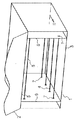
FIG. 1 is a perspective view of a rectangular parallelepiped (rectangular) shape in which the side length of a receiving space of an electric device (not shown) whose electromagnetic sensitivity is to be measured according to EMC standards is 1 to 2 meters, for example. 1 shows an overall view of an EMC test cell of the present invention. A flip-up door 2 is provided on one side wall of the chamber 1. A plurality of conductor wires 4, specifically, four conductor wires in the present embodiment, are separated from the floor surface of the chamber 1 by a spacing “a” from the inner floor surface that is one of the
[0011]
As the schematic circuit diagram according to FIG. 3 shows, the conductor wires 4 and 6 are fed at one end through a feed line distribution with a phase shift of 180 ° relative to each other, and the other end is made of metal via a
[0012]
The two sets of conductor wires 4 and 6 arranged opposite to each other are electrically fed from the balance-
[0013]
This functional interaction between a symmetric feed system and an asymmetric line system results in a two-wire line being terminated with a relatively low impedance termination impedance (the characteristic impedance of the stripline) and formed in parallel with it With respect to the characteristic impedance of the relatively high impedance of the equation line, there is no need to consider the dimensions at the end. On the input side, a termination impedance equal to the characteristic impedance of the stripline will work in series, and the input impedance will also be kept at a relatively low impedance, which is advantageous for feeding. Thanks to such a combined effect, a very uniform electric field strength distribution can be obtained in the chamber.
[0014]
The
Further, it is also preferable to provide an
In particular, in order to avoid disturbing reflections that occur in the high-frequency region, an additional high-
[0015]
【The invention's effect】
According to the present invention, it is possible to provide the maximum test space that can be used within a given minimum space, and to ensure a uniform electric field strength distribution in the chamber as required by strict standards.
[Brief description of the drawings]
FIG. 1 is a perspective view of an EMC test cell of an example.
FIG. 2 is a cross-sectional view of the embodiment of FIG.
FIG. 3 is a schematic circuit diagram of the embodiment of FIG. 1;
[Explanation of symbols]
DESCRIPTION OF SYMBOLS 1 Chamber 2
Claims (5)
高周波電源から給電された高周波電磁界をチャンバー内に発生させる発生手段と、
前記チャンバーの対向する両側面間に配置された少なくとも2本の導体線と、
を有し、
前記少なくとも2本の導体線は、前記チャンバーの前記両側面のうちの一つの側面を形成する一つのチャンバー壁から間隔をあけて且つ前記一つのチャンバー壁と平行になるように配置された少なくとも1本の導体線と、前記チャンバーの前記両側面のうちの他の側面を形成する他のチャンバー壁から間隔をあけて且つ前記他のチャンバー壁と平行になるように配置された少なくとも1本の導体線と、を含み、1つの対称型の二線式の線路を形成し、その1端において前記高周波電源から前記発生手段によって逆相に給電され、他端において終端インピーダンスを介してチャンバー壁に電気的に接続される、
電気装置のEMC試験装置。A chamber of conductive material;
Generating means for generating a high-frequency electromagnetic field fed from a high-frequency power source in the chamber ;
At least two conductor wires disposed between opposite sides of the chamber;
Have
The at least two conductor lines are at least one disposed at a distance from and parallel to the one chamber wall forming one side surface of the both side surfaces of the chamber. And at least one conductor disposed at a distance from and parallel to the other chamber wall forming the other side surface of the both side surfaces of the chamber wherein the line, and forms one symmetric two-wire lines, are fed in opposite phase by said generating means from said high frequency power source at its one end, electricity chamber wall via a terminating impedance at the other end Connected,
EMC testing equipment for electrical equipment.
を特徴とする請求項1による電気装置のEMC試験装置。The EMC test apparatus for an electrical apparatus according to claim 1, wherein the termination impedance is sized so as to correspond to a characteristic impedance formed between the chamber wall and the conductor wire.
を特徴とする請求項1、2または3による電気装置のEMC試験装置。4. The EMC test apparatus for an electrical device according to claim 1, wherein the mutual distance between the conductor wires and / or the termination impedance are individually adjusted in size so as to give a predetermined electric field strength distribution.
を特徴とする請求項1、2、3または4による電気装置のEMC試験装置。The EMC test apparatus for an electric device according to claim 1, 2, 3, or 4, wherein the high-frequency absorber is attached to the inside of at least one side wall of the chamber.
Applications Claiming Priority (2)
| Application Number | Priority Date | Filing Date | Title |
|---|---|---|---|
| DE19549134.3 | 1995-12-29 | ||
| DE19549134A DE19549134B4 (en) | 1995-12-29 | 1995-12-29 | Device for EMC testing of electrical equipment |
Publications (2)
| Publication Number | Publication Date |
|---|---|
| JPH09196994A JPH09196994A (en) | 1997-07-31 |
| JP4044983B2 true JP4044983B2 (en) | 2008-02-06 |
Family
ID=7781639
Family Applications (1)
| Application Number | Title | Priority Date | Filing Date |
|---|---|---|---|
| JP34888196A Expired - Lifetime JP4044983B2 (en) | 1995-12-29 | 1996-12-26 | EMC testing equipment for electrical equipment |
Country Status (4)
| Country | Link |
|---|---|
| US (1) | US5942903A (en) |
| EP (1) | EP0782003B1 (en) |
| JP (1) | JP4044983B2 (en) |
| DE (2) | DE19549134B4 (en) |
Families Citing this family (1)
| Publication number | Priority date | Publication date | Assignee | Title |
|---|---|---|---|---|
| EP1110095B1 (en) * | 1998-08-24 | 2008-10-08 | BRITISH TELECOMMUNICATIONS public limited company | Method and apparatus for electromagnetic emissions testing |
Family Cites Families (12)
| Publication number | Priority date | Publication date | Assignee | Title |
|---|---|---|---|---|
| US2446195A (en) * | 1945-03-14 | 1948-08-03 | Us Sec War | Tester for electrical shieldings |
| DE3130487A1 (en) * | 1981-07-23 | 1983-02-10 | Licentia Patent-Verwaltungs-Gmbh, 6000 Frankfurt | Low-reflection, shielded, metallic simulation chamber for electromagnetic radiation |
| DE3842196C2 (en) * | 1987-09-17 | 1994-05-05 | Deutsche Aerospace | Shielded cell for the generation of electromagnetic waves of the transverse electrical type |
| DE3731165A1 (en) * | 1987-09-17 | 1989-03-30 | Licentia Gmbh | SHIELDED CELL FOR GENERATING ELECTROMAGNETIC WAVES OF THE TRANSVERSAL-ELECTRICAL TYPE |
| DE3931449A1 (en) * | 1988-10-22 | 1990-03-08 | Telefunken Systemtechnik | Funnel-shaped waveguide with transit time equalisation - has spherical absorber wall directly adjacent conductive housing rear wall of similar shape |
| DE3925247C2 (en) * | 1989-07-29 | 1994-03-03 | Deutsche Aerospace | Arrangement for generating and receiving defined field strengths |
| ES2048579T3 (en) * | 1991-06-11 | 1994-03-16 | Amplisilence Srl | DEVICE FOR MEASURING ELECTROMAGNETIC INTERFERENCE. |
| CA2047999C (en) * | 1991-07-30 | 2000-10-31 | Gary A. Gibson | Broadband electromagnetic field simulator |
| US5285164A (en) * | 1992-07-30 | 1994-02-08 | Northern Telecom Limited | Electromagnetic radiation measurement apparatus |
| DE4300778A1 (en) * | 1993-01-14 | 1994-07-21 | Puls Plasmatechnik Gmbh | Transverse em or TEM cell, esp. for investigating electromagnetic compatibility |
| US5436603A (en) * | 1993-09-27 | 1995-07-25 | Fischer Custom Communications, Inc. | Transverse electromagnetic cell |
| DE19549246C1 (en) * | 1995-12-21 | 1997-04-10 | Hansen Euro Emc Service Gmbh | Electromagnetic wave generation and reception method for immunity testing |
-
1995
- 1995-12-29 DE DE19549134A patent/DE19549134B4/en not_active Expired - Lifetime
-
1996
- 1996-11-16 EP EP96118415A patent/EP0782003B1/en not_active Expired - Lifetime
- 1996-11-16 DE DE59611220T patent/DE59611220D1/en not_active Expired - Lifetime
- 1996-11-22 US US08/754,153 patent/US5942903A/en not_active Expired - Lifetime
- 1996-12-26 JP JP34888196A patent/JP4044983B2/en not_active Expired - Lifetime
Also Published As
| Publication number | Publication date |
|---|---|
| DE19549134B4 (en) | 2005-04-07 |
| DE59611220D1 (en) | 2005-05-25 |
| DE19549134A1 (en) | 1997-07-03 |
| US5942903A (en) | 1999-08-24 |
| EP0782003A3 (en) | 1998-04-01 |
| EP0782003B1 (en) | 2005-04-20 |
| EP0782003A2 (en) | 1997-07-02 |
| JPH09196994A (en) | 1997-07-31 |
Similar Documents
| Publication | Publication Date | Title |
|---|---|---|
| US5440316A (en) | Broadband antennas and electromagnetic field simulators | |
| US5514971A (en) | Method and apparatus for testing an immunity to electromagnetic interference and apparatus for irradiating radio wave for immunity test | |
| JP4044983B2 (en) | EMC testing equipment for electrical equipment | |
| US5436603A (en) | Transverse electromagnetic cell | |
| US9470731B1 (en) | Transverse electromagnetic cell | |
| JP3187790B2 (en) | Linear coupled transmission line cell | |
| US4232319A (en) | Broadband transmitting antenna for test chamber | |
| JP3880727B2 (en) | TEM cell | |
| US5844413A (en) | Method and apparatus for generating and receiving electromagnetic waves for testing purposes | |
| RU2465610C2 (en) | Tunable antenna for electromagnetic compatibility tests | |
| US5861753A (en) | Electromagnetic compatibility (EMC) test cell | |
| JP2738507B2 (en) | Cell for small electromagnetic wave measurement and strong electromagnetic wave generation | |
| RU2014625C1 (en) | Gear for testing of radio electronic equipment in current-conducting cases for resistance to action of electromagnetic field | |
| KR100340038B1 (en) | Appartus of ems test for vehicle | |
| Chamnankij et al. | Frequency Enhancement of Gigahertz Transverse Electromagnetic Cell for EMC Calibration in 300 kHz–6 GHz | |
| CN113253036B (en) | Darkroom reconfigurable strip line for electromagnetic compatibility test | |
| JPH1130638A (en) | Wide-band electromagnetic wave testing black box | |
| KR0144869B1 (en) | 3p-tem cell | |
| KR20010083382A (en) | Standard fields generation cell for emc testing and calibration | |
| ATE344971T1 (en) | INSULATOR FOR ELECTRICAL CONDUCTORS WITH EXTERNAL SHIELDING. | |
| KR100238445B1 (en) | E-field and h-field generation system with 8p-vwig | |
| Ishigami et al. | Improvement of folded rhombic antenna for transient electromagnetic-field radiator | |
| Coenen | Shielding Effectiveness Measurements DC to 40 GHz, draft IEEE 2855 | |
| GB2125226A (en) | Electrical transmission cells for producing calculable e.m. fields | |
| EP0821242A2 (en) | An electromagnetic compatibility (EMC) test cell |
Legal Events
| Date | Code | Title | Description |
|---|---|---|---|
| A131 | Notification of reasons for refusal |
Free format text: JAPANESE INTERMEDIATE CODE: A131 Effective date: 20060926 |
|
| A521 | Request for written amendment filed |
Free format text: JAPANESE INTERMEDIATE CODE: A523 Effective date: 20061226 |
|
| RD13 | Notification of appointment of power of sub attorney |
Free format text: JAPANESE INTERMEDIATE CODE: A7433 Effective date: 20061226 |
|
| A521 | Request for written amendment filed |
Free format text: JAPANESE INTERMEDIATE CODE: A821 Effective date: 20061226 |
|
| A131 | Notification of reasons for refusal |
Free format text: JAPANESE INTERMEDIATE CODE: A131 Effective date: 20070703 |
|
| A521 | Request for written amendment filed |
Free format text: JAPANESE INTERMEDIATE CODE: A523 Effective date: 20071002 |
|
| TRDD | Decision of grant or rejection written | ||
| A01 | Written decision to grant a patent or to grant a registration (utility model) |
Free format text: JAPANESE INTERMEDIATE CODE: A01 Effective date: 20071106 |
|
| A61 | First payment of annual fees (during grant procedure) |
Free format text: JAPANESE INTERMEDIATE CODE: A61 Effective date: 20071119 |
|
| R150 | Certificate of patent or registration of utility model |
Free format text: JAPANESE INTERMEDIATE CODE: R150 |
|
| FPAY | Renewal fee payment (event date is renewal date of database) |
Free format text: PAYMENT UNTIL: 20101122 Year of fee payment: 3 |
|
| FPAY | Renewal fee payment (event date is renewal date of database) |
Free format text: PAYMENT UNTIL: 20111122 Year of fee payment: 4 |
|
| FPAY | Renewal fee payment (event date is renewal date of database) |
Free format text: PAYMENT UNTIL: 20121122 Year of fee payment: 5 |
|
| FPAY | Renewal fee payment (event date is renewal date of database) |
Free format text: PAYMENT UNTIL: 20131122 Year of fee payment: 6 |
|
| R250 | Receipt of annual fees |
Free format text: JAPANESE INTERMEDIATE CODE: R250 |
|
| R250 | Receipt of annual fees |
Free format text: JAPANESE INTERMEDIATE CODE: R250 |
|
| R250 | Receipt of annual fees |
Free format text: JAPANESE INTERMEDIATE CODE: R250 |
|
| EXPY | Cancellation because of completion of term |