JP4044568B2 - Pixel circuit, light emitting device, and semiconductor device - Google Patents
Pixel circuit, light emitting device, and semiconductor device Download PDFInfo
- Publication number
- JP4044568B2 JP4044568B2 JP2005064611A JP2005064611A JP4044568B2 JP 4044568 B2 JP4044568 B2 JP 4044568B2 JP 2005064611 A JP2005064611 A JP 2005064611A JP 2005064611 A JP2005064611 A JP 2005064611A JP 4044568 B2 JP4044568 B2 JP 4044568B2
- Authority
- JP
- Japan
- Prior art keywords
- transistor
- electrode
- electrically connected
- source
- gate
- Prior art date
- Legal status (The legal status is an assumption and is not a legal conclusion. Google has not performed a legal analysis and makes no representation as to the accuracy of the status listed.)
- Expired - Fee Related
Links
- 239000004065 semiconductor Substances 0.000 title claims description 40
- 239000003990 capacitor Substances 0.000 claims description 153
- 239000010409 thin film Substances 0.000 claims description 6
- 239000010408 film Substances 0.000 description 363
- 239000010410 layer Substances 0.000 description 196
- 238000005401 electroluminescence Methods 0.000 description 100
- 238000000034 method Methods 0.000 description 96
- 229910052581 Si3N4 Inorganic materials 0.000 description 75
- HQVNEWCFYHHQES-UHFFFAOYSA-N silicon nitride Chemical compound N12[Si]34N5[Si]62N3[Si]51N64 HQVNEWCFYHHQES-UHFFFAOYSA-N 0.000 description 75
- 239000011229 interlayer Substances 0.000 description 68
- 239000012535 impurity Substances 0.000 description 61
- 239000000463 material Substances 0.000 description 56
- 239000000758 substrate Substances 0.000 description 37
- 238000005070 sampling Methods 0.000 description 30
- 238000002347 injection Methods 0.000 description 27
- 239000007924 injection Substances 0.000 description 27
- 238000005268 plasma chemical vapour deposition Methods 0.000 description 25
- 230000008569 process Effects 0.000 description 24
- 238000010438 heat treatment Methods 0.000 description 22
- XUIMIQQOPSSXEZ-UHFFFAOYSA-N Silicon Chemical compound [Si] XUIMIQQOPSSXEZ-UHFFFAOYSA-N 0.000 description 21
- 238000010586 diagram Methods 0.000 description 21
- 238000005530 etching Methods 0.000 description 21
- 229910052710 silicon Inorganic materials 0.000 description 21
- 239000010703 silicon Substances 0.000 description 21
- NIXOWILDQLNWCW-UHFFFAOYSA-N acrylic acid group Chemical group C(C=C)(=O)O NIXOWILDQLNWCW-UHFFFAOYSA-N 0.000 description 15
- 230000005525 hole transport Effects 0.000 description 15
- 238000012937 correction Methods 0.000 description 14
- QVGXLLKOCUKJST-UHFFFAOYSA-N atomic oxygen Chemical compound [O] QVGXLLKOCUKJST-UHFFFAOYSA-N 0.000 description 13
- 238000006243 chemical reaction Methods 0.000 description 13
- 239000001301 oxygen Substances 0.000 description 13
- 229910052760 oxygen Inorganic materials 0.000 description 13
- 239000000126 substance Substances 0.000 description 13
- 238000011282 treatment Methods 0.000 description 13
- XLOMVQKBTHCTTD-UHFFFAOYSA-N Zinc monoxide Chemical compound [Zn]=O XLOMVQKBTHCTTD-UHFFFAOYSA-N 0.000 description 12
- 238000000137 annealing Methods 0.000 description 12
- 229910052782 aluminium Inorganic materials 0.000 description 11
- 229910021417 amorphous silicon Inorganic materials 0.000 description 11
- 239000007789 gas Substances 0.000 description 11
- 230000015572 biosynthetic process Effects 0.000 description 10
- 238000004544 sputter deposition Methods 0.000 description 10
- OKTJSMMVPCPJKN-UHFFFAOYSA-N Carbon Chemical compound [C] OKTJSMMVPCPJKN-UHFFFAOYSA-N 0.000 description 9
- 239000011521 glass Substances 0.000 description 9
- 229910003437 indium oxide Inorganic materials 0.000 description 9
- PJXISJQVUVHSOJ-UHFFFAOYSA-N indium(iii) oxide Chemical compound [O-2].[O-2].[O-2].[In+3].[In+3] PJXISJQVUVHSOJ-UHFFFAOYSA-N 0.000 description 9
- 238000004519 manufacturing process Methods 0.000 description 9
- 239000002356 single layer Substances 0.000 description 9
- IJGRMHOSHXDMSA-UHFFFAOYSA-N Atomic nitrogen Chemical compound N#N IJGRMHOSHXDMSA-UHFFFAOYSA-N 0.000 description 8
- 239000012298 atmosphere Substances 0.000 description 8
- 229910052799 carbon Inorganic materials 0.000 description 8
- 150000001875 compounds Chemical class 0.000 description 8
- 238000002425 crystallisation Methods 0.000 description 8
- 230000014509 gene expression Effects 0.000 description 8
- 238000005984 hydrogenation reaction Methods 0.000 description 8
- 230000001681 protective effect Effects 0.000 description 8
- 239000013078 crystal Substances 0.000 description 7
- 239000003566 sealing material Substances 0.000 description 7
- UFHFLCQGNIYNRP-UHFFFAOYSA-N Hydrogen Chemical compound [H][H] UFHFLCQGNIYNRP-UHFFFAOYSA-N 0.000 description 6
- 230000001133 acceleration Effects 0.000 description 6
- 238000001994 activation Methods 0.000 description 6
- 239000000956 alloy Substances 0.000 description 6
- XAGFODPZIPBFFR-UHFFFAOYSA-N aluminium Chemical compound [Al] XAGFODPZIPBFFR-UHFFFAOYSA-N 0.000 description 6
- QVQLCTNNEUAWMS-UHFFFAOYSA-N barium oxide Chemical compound [Ba]=O QVQLCTNNEUAWMS-UHFFFAOYSA-N 0.000 description 6
- 239000001257 hydrogen Substances 0.000 description 6
- 229910052739 hydrogen Inorganic materials 0.000 description 6
- 239000011159 matrix material Substances 0.000 description 6
- 229910052751 metal Inorganic materials 0.000 description 6
- 238000000059 patterning Methods 0.000 description 6
- 238000003860 storage Methods 0.000 description 6
- XOLBLPGZBRYERU-UHFFFAOYSA-N tin dioxide Chemical compound O=[Sn]=O XOLBLPGZBRYERU-UHFFFAOYSA-N 0.000 description 6
- 229910001887 tin oxide Inorganic materials 0.000 description 6
- 239000011787 zinc oxide Substances 0.000 description 6
- OAICVXFJPJFONN-UHFFFAOYSA-N Phosphorus Chemical compound [P] OAICVXFJPJFONN-UHFFFAOYSA-N 0.000 description 5
- 229910045601 alloy Inorganic materials 0.000 description 5
- 238000005229 chemical vapour deposition Methods 0.000 description 5
- 230000008025 crystallization Effects 0.000 description 5
- 230000006866 deterioration Effects 0.000 description 5
- 150000002500 ions Chemical class 0.000 description 5
- 239000002184 metal Substances 0.000 description 5
- 230000003287 optical effect Effects 0.000 description 5
- 238000002161 passivation Methods 0.000 description 5
- 229910052698 phosphorus Inorganic materials 0.000 description 5
- 239000011574 phosphorus Substances 0.000 description 5
- 229920003023 plastic Polymers 0.000 description 5
- 239000004033 plastic Substances 0.000 description 5
- 229910021420 polycrystalline silicon Inorganic materials 0.000 description 5
- 229920005989 resin Polymers 0.000 description 5
- 239000011347 resin Substances 0.000 description 5
- 238000001039 wet etching Methods 0.000 description 5
- 239000004925 Acrylic resin Substances 0.000 description 4
- 229920000178 Acrylic resin Polymers 0.000 description 4
- 230000004913 activation Effects 0.000 description 4
- 239000008186 active pharmaceutical agent Substances 0.000 description 4
- UMIVXZPTRXBADB-UHFFFAOYSA-N benzocyclobutene Chemical compound C1=CC=C2CCC2=C1 UMIVXZPTRXBADB-UHFFFAOYSA-N 0.000 description 4
- 229910052802 copper Inorganic materials 0.000 description 4
- 239000010949 copper Substances 0.000 description 4
- 229910021419 crystalline silicon Inorganic materials 0.000 description 4
- 239000000945 filler Substances 0.000 description 4
- 239000002923 metal particle Substances 0.000 description 4
- 229910052757 nitrogen Inorganic materials 0.000 description 4
- 239000002245 particle Substances 0.000 description 4
- 238000012545 processing Methods 0.000 description 4
- 239000000565 sealant Substances 0.000 description 4
- VYPSYNLAJGMNEJ-UHFFFAOYSA-N silicon dioxide Inorganic materials O=[Si]=O VYPSYNLAJGMNEJ-UHFFFAOYSA-N 0.000 description 4
- 229910052719 titanium Inorganic materials 0.000 description 4
- GYHNNYVSQQEPJS-UHFFFAOYSA-N Gallium Chemical compound [Ga] GYHNNYVSQQEPJS-UHFFFAOYSA-N 0.000 description 3
- 239000004642 Polyimide Substances 0.000 description 3
- 238000001312 dry etching Methods 0.000 description 3
- 239000000975 dye Substances 0.000 description 3
- 229910052733 gallium Inorganic materials 0.000 description 3
- 239000004973 liquid crystal related substance Substances 0.000 description 3
- 230000010355 oscillation Effects 0.000 description 3
- 239000000049 pigment Substances 0.000 description 3
- 229920001721 polyimide Polymers 0.000 description 3
- 229920000642 polymer Polymers 0.000 description 3
- 229920005591 polysilicon Polymers 0.000 description 3
- 229920002620 polyvinyl fluoride Polymers 0.000 description 3
- 229910052814 silicon oxide Inorganic materials 0.000 description 3
- 229910052709 silver Inorganic materials 0.000 description 3
- 239000004332 silver Substances 0.000 description 3
- 238000007740 vapor deposition Methods 0.000 description 3
- YLYPIBBGWLKELC-RMKNXTFCSA-N 2-[2-[(e)-2-[4-(dimethylamino)phenyl]ethenyl]-6-methylpyran-4-ylidene]propanedinitrile Chemical compound C1=CC(N(C)C)=CC=C1\C=C\C1=CC(=C(C#N)C#N)C=C(C)O1 YLYPIBBGWLKELC-RMKNXTFCSA-N 0.000 description 2
- XKRFYHLGVUSROY-UHFFFAOYSA-N Argon Chemical compound [Ar] XKRFYHLGVUSROY-UHFFFAOYSA-N 0.000 description 2
- 229920002799 BoPET Polymers 0.000 description 2
- WHXSMMKQMYFTQS-UHFFFAOYSA-N Lithium Chemical compound [Li] WHXSMMKQMYFTQS-UHFFFAOYSA-N 0.000 description 2
- FYYHWMGAXLPEAU-UHFFFAOYSA-N Magnesium Chemical compound [Mg] FYYHWMGAXLPEAU-UHFFFAOYSA-N 0.000 description 2
- 239000005041 Mylar™ Substances 0.000 description 2
- 229910052779 Neodymium Inorganic materials 0.000 description 2
- PXHVJJICTQNCMI-UHFFFAOYSA-N Nickel Chemical compound [Ni] PXHVJJICTQNCMI-UHFFFAOYSA-N 0.000 description 2
- 229920001609 Poly(3,4-ethylenedioxythiophene) Polymers 0.000 description 2
- 239000004952 Polyamide Substances 0.000 description 2
- NRCMAYZCPIVABH-UHFFFAOYSA-N Quinacridone Chemical compound N1C2=CC=CC=C2C(=O)C2=C1C=C1C(=O)C3=CC=CC=C3NC1=C2 NRCMAYZCPIVABH-UHFFFAOYSA-N 0.000 description 2
- BOTDANWDWHJENH-UHFFFAOYSA-N Tetraethyl orthosilicate Chemical compound CCO[Si](OCC)(OCC)OCC BOTDANWDWHJENH-UHFFFAOYSA-N 0.000 description 2
- DQXBYHZEEUGOBF-UHFFFAOYSA-N but-3-enoic acid;ethene Chemical compound C=C.OC(=O)CC=C DQXBYHZEEUGOBF-UHFFFAOYSA-N 0.000 description 2
- 239000010406 cathode material Substances 0.000 description 2
- 230000008859 change Effects 0.000 description 2
- 229910052804 chromium Inorganic materials 0.000 description 2
- 239000003086 colorant Substances 0.000 description 2
- 239000011231 conductive filler Substances 0.000 description 2
- 229920000547 conjugated polymer Polymers 0.000 description 2
- XCJYREBRNVKWGJ-UHFFFAOYSA-N copper(II) phthalocyanine Chemical compound [Cu+2].C12=CC=CC=C2C(N=C2[N-]C(C3=CC=CC=C32)=N2)=NC1=NC([C]1C=CC=CC1=1)=NC=1N=C1[C]3C=CC=CC3=C2[N-]1 XCJYREBRNVKWGJ-UHFFFAOYSA-N 0.000 description 2
- ZYGHJZDHTFUPRJ-UHFFFAOYSA-N coumarin Chemical compound C1=CC=C2OC(=O)C=CC2=C1 ZYGHJZDHTFUPRJ-UHFFFAOYSA-N 0.000 description 2
- 238000007872 degassing Methods 0.000 description 2
- 230000005611 electricity Effects 0.000 description 2
- 125000005678 ethenylene group Chemical group [H]C([*:1])=C([H])[*:2] 0.000 description 2
- 239000005038 ethylene vinyl acetate Substances 0.000 description 2
- 230000005281 excited state Effects 0.000 description 2
- 239000011152 fibreglass Substances 0.000 description 2
- 239000007850 fluorescent dye Substances 0.000 description 2
- 230000005283 ground state Effects 0.000 description 2
- RBTKNAXYKSUFRK-UHFFFAOYSA-N heliogen blue Chemical compound [Cu].[N-]1C2=C(C=CC=C3)C3=C1N=C([N-]1)C3=CC=CC=C3C1=NC([N-]1)=C(C=CC=C3)C3=C1N=C([N-]1)C3=CC=CC=C3C1=N2 RBTKNAXYKSUFRK-UHFFFAOYSA-N 0.000 description 2
- 238000009616 inductively coupled plasma Methods 0.000 description 2
- 229910010272 inorganic material Inorganic materials 0.000 description 2
- 239000011147 inorganic material Substances 0.000 description 2
- 239000005001 laminate film Substances 0.000 description 2
- 238000005224 laser annealing Methods 0.000 description 2
- 238000005499 laser crystallization Methods 0.000 description 2
- 229910052744 lithium Inorganic materials 0.000 description 2
- 229910052749 magnesium Inorganic materials 0.000 description 2
- 239000011777 magnesium Substances 0.000 description 2
- 239000012299 nitrogen atmosphere Substances 0.000 description 2
- 239000011368 organic material Substances 0.000 description 2
- 238000004806 packaging method and process Methods 0.000 description 2
- 230000000737 periodic effect Effects 0.000 description 2
- 125000002080 perylenyl group Chemical group C1(=CC=C2C=CC=C3C4=CC=CC5=CC=CC(C1=C23)=C45)* 0.000 description 2
- CSHWQDPOILHKBI-UHFFFAOYSA-N peryrene Natural products C1=CC(C2=CC=CC=3C2=C2C=CC=3)=C3C2=CC=CC3=C1 CSHWQDPOILHKBI-UHFFFAOYSA-N 0.000 description 2
- 238000000206 photolithography Methods 0.000 description 2
- 229920001200 poly(ethylene-vinyl acetate) Polymers 0.000 description 2
- 229920002037 poly(vinyl butyral) polymer Polymers 0.000 description 2
- 229920002647 polyamide Polymers 0.000 description 2
- 229920006267 polyester film Polymers 0.000 description 2
- 229920000123 polythiophene Polymers 0.000 description 2
- 229920000915 polyvinyl chloride Polymers 0.000 description 2
- 239000004800 polyvinyl chloride Substances 0.000 description 2
- 238000004151 rapid thermal annealing Methods 0.000 description 2
- 238000007789 sealing Methods 0.000 description 2
- HBMJWWWQQXIZIP-UHFFFAOYSA-N silicon carbide Chemical compound [Si+]#[C-] HBMJWWWQQXIZIP-UHFFFAOYSA-N 0.000 description 2
- 229910010271 silicon carbide Inorganic materials 0.000 description 2
- 238000004528 spin coating Methods 0.000 description 2
- 239000010935 stainless steel Substances 0.000 description 2
- 229910001220 stainless steel Inorganic materials 0.000 description 2
- 230000003068 static effect Effects 0.000 description 2
- 238000000859 sublimation Methods 0.000 description 2
- 230000008022 sublimation Effects 0.000 description 2
- ZOXJGFHDIHLPTG-UHFFFAOYSA-N Boron Chemical compound [B] ZOXJGFHDIHLPTG-UHFFFAOYSA-N 0.000 description 1
- 229910052684 Cerium Inorganic materials 0.000 description 1
- RYGMFSIKBFXOCR-UHFFFAOYSA-N Copper Chemical compound [Cu] RYGMFSIKBFXOCR-UHFFFAOYSA-N 0.000 description 1
- 229910052691 Erbium Inorganic materials 0.000 description 1
- 229910052689 Holmium Inorganic materials 0.000 description 1
- BQCADISMDOOEFD-UHFFFAOYSA-N Silver Chemical compound [Ag] BQCADISMDOOEFD-UHFFFAOYSA-N 0.000 description 1
- LEVVHYCKPQWKOP-UHFFFAOYSA-N [Si].[Ge] Chemical compound [Si].[Ge] LEVVHYCKPQWKOP-UHFFFAOYSA-N 0.000 description 1
- 239000005407 aluminoborosilicate glass Substances 0.000 description 1
- 229910052786 argon Inorganic materials 0.000 description 1
- 229910052785 arsenic Inorganic materials 0.000 description 1
- RQNWIZPPADIBDY-UHFFFAOYSA-N arsenic atom Chemical compound [As] RQNWIZPPADIBDY-UHFFFAOYSA-N 0.000 description 1
- 229910052788 barium Inorganic materials 0.000 description 1
- DSAJWYNOEDNPEQ-UHFFFAOYSA-N barium atom Chemical compound [Ba] DSAJWYNOEDNPEQ-UHFFFAOYSA-N 0.000 description 1
- 230000008901 benefit Effects 0.000 description 1
- 230000000903 blocking effect Effects 0.000 description 1
- 229910052796 boron Inorganic materials 0.000 description 1
- 239000005388 borosilicate glass Substances 0.000 description 1
- 239000002041 carbon nanotube Substances 0.000 description 1
- 229910021393 carbon nanotube Inorganic materials 0.000 description 1
- 229910010293 ceramic material Inorganic materials 0.000 description 1
- 239000011248 coating agent Substances 0.000 description 1
- 238000000576 coating method Methods 0.000 description 1
- 238000004891 communication Methods 0.000 description 1
- 229960000956 coumarin Drugs 0.000 description 1
- 235000001671 coumarin Nutrition 0.000 description 1
- 230000008878 coupling Effects 0.000 description 1
- 238000010168 coupling process Methods 0.000 description 1
- 238000005859 coupling reaction Methods 0.000 description 1
- 238000005520 cutting process Methods 0.000 description 1
- 230000007547 defect Effects 0.000 description 1
- 238000011161 development Methods 0.000 description 1
- ZOCHARZZJNPSEU-UHFFFAOYSA-N diboron Chemical compound B#B ZOCHARZZJNPSEU-UHFFFAOYSA-N 0.000 description 1
- 238000007599 discharging Methods 0.000 description 1
- 239000006185 dispersion Substances 0.000 description 1
- 230000000694 effects Effects 0.000 description 1
- 230000005684 electric field Effects 0.000 description 1
- 238000005516 engineering process Methods 0.000 description 1
- 239000003822 epoxy resin Substances 0.000 description 1
- 230000002349 favourable effect Effects 0.000 description 1
- 230000005669 field effect Effects 0.000 description 1
- 239000011888 foil Substances 0.000 description 1
- AMGQUBHHOARCQH-UHFFFAOYSA-N indium;oxotin Chemical compound [In].[Sn]=O AMGQUBHHOARCQH-UHFFFAOYSA-N 0.000 description 1
- 239000011261 inert gas Substances 0.000 description 1
- 239000012212 insulator Substances 0.000 description 1
- 238000005468 ion implantation Methods 0.000 description 1
- 238000004518 low pressure chemical vapour deposition Methods 0.000 description 1
- 238000004020 luminiscence type Methods 0.000 description 1
- 239000007769 metal material Substances 0.000 description 1
- 229910052750 molybdenum Inorganic materials 0.000 description 1
- 239000000178 monomer Substances 0.000 description 1
- 229910052759 nickel Inorganic materials 0.000 description 1
- 230000003647 oxidation Effects 0.000 description 1
- 238000007254 oxidation reaction Methods 0.000 description 1
- 239000002985 plastic film Substances 0.000 description 1
- 229920006255 plastic film Polymers 0.000 description 1
- 229920000647 polyepoxide Polymers 0.000 description 1
- 238000003825 pressing Methods 0.000 description 1
- 239000010453 quartz Substances 0.000 description 1
- 239000012495 reaction gas Substances 0.000 description 1
- 230000004044 response Effects 0.000 description 1
- 239000010979 ruby Substances 0.000 description 1
- 229910001750 ruby Inorganic materials 0.000 description 1
- 239000007787 solid Substances 0.000 description 1
- 239000000243 solution Substances 0.000 description 1
- 229910052715 tantalum Inorganic materials 0.000 description 1
- 238000002230 thermal chemical vapour deposition Methods 0.000 description 1
- 229920001187 thermosetting polymer Polymers 0.000 description 1
- 238000012546 transfer Methods 0.000 description 1
- 239000012780 transparent material Substances 0.000 description 1
- 229910052721 tungsten Inorganic materials 0.000 description 1
- NXHILIPIEUBEPD-UHFFFAOYSA-H tungsten hexafluoride Chemical compound F[W](F)(F)(F)(F)F NXHILIPIEUBEPD-UHFFFAOYSA-H 0.000 description 1
Images


Description
本発明は、トランジスタを有する発光装置の構成に関する。本発明は特に、ガラス、プラスチック等の絶縁体上に作製される薄膜トランジスタ(以後、TFTと表記する)を有するアクティブマトリクス型発光装置の構成に関する。また、このような発光装置を表示部に用いた電子機器に関する。 The present invention relates to a structure of a light emitting device having a transistor. The present invention particularly relates to a structure of an active matrix light-emitting device having a thin film transistor (hereinafter referred to as a TFT) manufactured on an insulator such as glass or plastic. The present invention also relates to an electronic device using such a light-emitting device for a display portion.
近年、エレクトロルミネッセンス(Electro Luminescence:EL)素子等を始めとした発光素子を用いた表示装置の開発が活発化している。発光素子は、自らが発光するために視認性が高く、液晶表示装置(LCD)等において必要なバックライトを必要としないために薄型化に適しているとともに、視野角にほとんど制限が無い。 In recent years, development of display devices using light-emitting elements such as electroluminescence (EL) elements has been activated. The light-emitting element has high visibility because it emits light by itself, and is suitable for thinning because it does not require a backlight necessary for a liquid crystal display (LCD) or the like, and has almost no restriction on the viewing angle.
ここで、EL素子とは、電場を加えることで発生するルミネッセンスが得られる発光層を有する素子を指す。この発光層においては、一重項励起状態から基底状態に戻る際の発光(蛍光)と、三重項励起状態から基底状態に戻る際の発光(燐光)とがあるが、本発明の発光装置は、上述したいずれの発光形態であっても良い。 Here, the EL element refers to an element having a light emitting layer from which luminescence generated by applying an electric field can be obtained. In this light emitting layer, there are light emission (fluorescence) when returning from the singlet excited state to the ground state, and light emission (phosphorescence) when returning from the triplet excited state to the ground state. Any of the light emission forms described above may be used.
EL素子は、一対の電極(陽極と陰極)間に発光層が挟まれる形で構成され、通常、積層構造をとっている。代表的には、イーストマン・コダック・カンパニーのTangらが提案した「陽極/正孔輸送層/発光層/電子輸送層/陰極」という積層構造が挙げられる。この構造は非常に発光効率が高く、現在研究が進められているEL素子の多くはこの構造が採用されている。 An EL element is configured such that a light emitting layer is sandwiched between a pair of electrodes (anode and cathode), and usually has a laminated structure. A typical example is a stacked structure of “anode / hole transport layer / light emitting layer / electron transport layer / cathode” proposed by Tang et al. Of Eastman Kodak Company. This structure has a very high luminous efficiency, and this structure is employed in many EL devices that are currently being studied.
また、これ以外にも、陽極と陰極との間に、「正孔注入層/正孔輸送層/発光層/電子輸送層」または「正孔注入層/正孔輸送層/発光層/電子輸送層/電子注入層」の順に積層する構造がある。本発明の発光装置に用いるEL素子の構造としては、上述の構造のいずれを採用していても良い。また、発光層に対して蛍光性色素等をドーピングしても良い。 In addition to this, between the anode and the cathode, “hole injection layer / hole transport layer / light emitting layer / electron transport layer” or “hole injection layer / hole transport layer / light emitting layer / electron transport”. There is a structure of stacking in the order of “layer / electron injection layer”. As the structure of the EL element used in the light emitting device of the present invention, any of the above structures may be adopted. Further, a fluorescent pigment or the like may be doped into the light emitting layer.
本発明においては、EL素子において、陽極と陰極との間に設けられる全ての層を総称してEL層と呼ぶ。よって、上述の正孔注入層、正孔輸送層、発光層、電子輸送層、電子注入層は、全てEL素子に含まれ、陽極、EL層、および陰極で構成される発光素子をEL素子と呼ぶ。 In the present invention, in the EL element, all layers provided between the anode and the cathode are collectively referred to as an EL layer. Therefore, the above-described hole injection layer, hole transport layer, light emitting layer, electron transport layer, and electron injection layer are all included in the EL element, and a light emitting element including an anode, an EL layer, and a cathode is referred to as an EL element. Call.
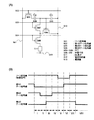
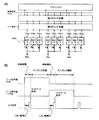
図3に、一般的な発光装置における画素の構成を示す。なお、代表的な発光装置として、EL表示装置を例とする。図3に示した画素は、ソース信号線301、ゲート信号線302、スイッチング用TFT303、駆動用TFT304、容量手段305、EL素子306、電流供給線307、電源308を有している。
FIG. 3 shows a structure of a pixel in a general light emitting device. Note that an EL display device is taken as an example of a typical light-emitting device. The pixel shown in FIG. 3 includes a
各部の接続関係について説明する。ここで、TFTはゲート、ソース、ドレインの3端子を有するが、ソース、ドレインに関しては、TFTの構造上、明確に区別が出来ない。よって、素子間の接続について説明する際は、ソース、ドレインのうち一方を第1の電極、他方を第2の電極と表記する。TFTのON、OFFについて、各端子の電位等(あるTFTのゲート・ソース間電圧等)について説明が必要な際には、ソース、ドレイン等と表記する。 The connection relationship of each part will be described. Here, the TFT has three terminals of a gate, a source, and a drain. However, the source and drain cannot be clearly distinguished because of the structure of the TFT. Therefore, when describing connection between elements, one of a source and a drain is referred to as a first electrode, and the other is referred to as a second electrode. Regarding the ON / OFF of a TFT, when it is necessary to explain the potential of each terminal (the voltage between the gate and the source of a TFT), it is expressed as a source, a drain, or the like.
また、本発明において、TFTがONしているとは、TFTのゲート・ソース間電圧がそのしきい値を超え、ソース、ドレイン間に電流が流れる状態をいい、TFTがOFFしているとは、TFTのゲート・ソース間電圧がそのしきい値を下回り、ソース、ドレイン間に電流が流れていない状態をいう。 In the present invention, the TFT is ON means that the voltage between the gate and the source of the TFT exceeds the threshold value and a current flows between the source and the drain. The TFT is OFF. In this state, the gate-source voltage of the TFT is below its threshold value, and no current flows between the source and drain.
スイッチング用TFT303のゲート電極は、ゲート信号線302に接続され、第1の電極はソース信号線301に接続され、第2の電極は駆動用TFT304のゲート電極に接続されている。駆動用TFT304の第1の電極は、電流供給線307に接続され、第2の電極はEL素子306の第1の電極に接続されている。EL素子306の第2の電極は、電源308に接続されている。容量手段305は、駆動用TFT304のゲート電極と第1の電極との間に接続され、駆動用TFT304のゲート・ソース間電圧を保持する。
A gate electrode of the switching
ゲート信号線302の電位が変化してスイッチング用TFT303がONすると、ソース信号線301に入力されている映像信号は、駆動用TFT304のゲート電極へと入力される。入力された映像信号の電位に従って、駆動用TFT304のゲート・ソース間電圧が決定し、駆動用TFT304のソース・ドレイン間を流れる電流(以下、ドレイン電流と表記)が決定する。この電流はEL素子306に供給されて発光する。
When the potential of the
ところで、多結晶シリコン(ポリシリコン 以下P−Si)で形成されたTFTは、非晶質シリコン(アモルファスシリコン 以下A−Si)で形成されたTFTよりも電界効果移動度が高く、ON電流が大きいため、発光装置に用いるトランジスタとしてより適している。 By the way, a TFT formed of polycrystalline silicon (polysilicon, hereinafter referred to as P-Si) has higher field effect mobility and a higher ON current than a TFT formed of amorphous silicon (amorphous silicon, hereinafter referred to as A-Si). Therefore, it is more suitable as a transistor used for a light-emitting device.
反面、ポリシリコンで形成されたTFTは、結晶粒界における欠陥に起因して、その電気的特性にばらつきが生じやすいといった問題点を有している。 On the other hand, TFTs formed of polysilicon have a problem that electrical characteristics are likely to vary due to defects in crystal grain boundaries.
図3に示した画素において、画素を構成するTFTのしきい値やON電流等の特性が画素ごとにばらつくと、同じ映像信号を入力した場合にも、それに応じてTFTのドレイン電流の大きさが異なってくるため、EL素子306の輝度がばらつく。よってアナログ階調の場合、問題となっていた。
In the pixel shown in FIG. 3, when the characteristics such as the threshold value and the ON current of the TFTs constituting the pixel vary from pixel to pixel, even when the same video signal is input, the magnitude of the drain current of the TFT is accordingly increased. Therefore, the luminance of the
そこで、TFTのしきい値等がON電流に影響しにくい領域を用いて、EL素子を輝度100%、0%の2つの状態のみで駆動するデジタル階調方式が提案されている。この方式では、白、黒の2階調しか表現出来ないため、時間階調方式等と組み合わせて多階調化を実現している。 Therefore, a digital gray scale method has been proposed in which the EL element is driven only in two states of luminance of 100% and 0% by using a region where the threshold value of the TFT hardly affects the ON current. Since this method can express only two gradations of white and black, multi-gradation is realized in combination with the time gradation method.
デジタル階調方式と時間階調方式とを組み合わせた方法を用いる場合の発光装置の画素の構成は、図4(A)(B)に示したようなものがある。スイッチング用TFT404、駆動用TFT405に加え、消去用TFT406を用いることによって、発光時間の長さを細かく制御することが可能となっている。
In the case of using a method combining a digital gray scale method and a time gray scale method, the pixel structure of the light emitting device is as shown in FIGS. By using the
一方、アナログ階調方式を用いて、TFTのしきい値ばらつきを補正することの出来るものが提案されている(例えば、特許文献1参照)。
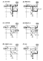
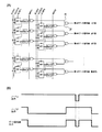
図5に示すように、ソース信号線501、第1〜第3のゲート信号線502〜504、TFT505〜508、容量手段509(C2)、510(C1)、電流供給線512、EL素子511を有する。
As shown in FIG. 5, a
TFT505のゲート電極は、第1のゲート信号線502に接続され、第1の電極は、ソース信号線501に接続され、第2の電極は、容量手段509の第1の電極に接続されている。容量手段509の第2の電極は、容量手段510の第1の電極に接続され、容量手段510の第2の電極は、電流供給線512に接続されている。TFT506のゲート電極は、容量手段509の第2の電極および容量手段510の第1の電極に接続され、第1の電極は、電流供給線512に接続され、第2の電極は、TFT507の第1の電極およびTFT508の第1の電極に接続されている。TFT507のゲート電極は、第2のゲート信号線503に接続され、第2の電極は、容量手段509の第2の電極および容量手段510の第1の電極に接続されている。TFT508のゲート電極は、第3のゲート信号線504に接続され、第2の電極は、EL素子511の第1の電極に接続されている。EL素子511の第2の電極には、電源513によって一定電位が与えられ、電流供給線512とは互いに電位差を有する。
The gate electrode of the
図5(B)および図6(A)〜(F)を用いて、動作について説明する。図5(B)は、ソース信号線501、第1〜第3のゲート信号線502〜504に入力される映像信号およびパルスのタイミングを示しており、図6に示す各動作にあわせて、I〜VIIIの区間に分割している。また、図5に示した画素の一例では、4つのTFTを用いて構成され、その極性は全てPチャネル型である。よって、ゲート電極にLレベルが入力されてONし、Hレベルが入力されてOFFするものとする。
The operation will be described with reference to FIGS. 5B and 6A to 6F. FIG. 5B shows timings of video signals and pulses inputted to the
まず、第1のゲート信号線502がLレベルとなり、TFT505がONする(区間I)。続いて第2、第3のゲート信号線がLレベルとなり、TFT507、508がONする。ここで、図6(A)に示すように、容量手段509、510が充電され、容量手段510が保持する電圧が、TFT506のしきい値(Vth)を上回ったところで、TFT506がONする(区間II)。
First, the first
続いて、第3のゲート信号線がHレベルとなって、TFT508がOFFする。すると、容量手段509、510に貯まっていた電荷が再び移動し、容量手段510に保持される電圧は、やがてVthに等しくなる。このとき、図6(B)にも示すように、電流供給線512、ソース信号線501の電位はいずれもVDDであるので、容量手段509においても、保持されている電圧はVthに等しくなる。よって、やがてTFT506はOFFする。
Subsequently, the third gate signal line becomes H level, and the
前述のように、容量手段509、510に保持されている電圧がVthに等しくなったところで、第2のゲート信号線503がHレベルとなり、TFT507がOFFする(区間IV)。この動作により、図6(C)に示すように、容量手段においてVthが保持される。
As described above, when the voltage held in the capacitor means 509 and 510 becomes equal to V th , the second
このとき、容量手段510(C1)に保持されている電荷Q1については、式(1)のような関係が成立する。同時に、容量手段509(C2)に保持されている電荷Q2においては、式(2)のような関係が成立する。 At this time, the relationship of the formula (1) is established for the charge Q 1 held in the capacitor means 510 (C 1 ). At the same time, in the charge Q 2 held in the capacitor means 509 (C 2 ), the relationship represented by the equation (2) is established.

続いて、図6(D)に示すように、映像信号の入力が行われる(区間V)。ソース信号線501に映像信号が出力されて、その電位はVDDから映像信号の電位VData(ここでは、TFT506がPチャネル型であるので、VDD>VDataとする。)となる。このときの、TFT506のゲート電極の電位をVPとし、このノードにおける電荷をQとすると、容量手段509、510とを含めた電荷保存則により、式(3)、(4)のような関係が成立する。
Subsequently, as shown in FIG. 6D, a video signal is input (section V). A video signal is output to the
式(1)〜(4)より、TFT506のゲート電極の電位VPは、式(5)で表される。
From the expressions (1) to (4), the potential V P of the gate electrode of the
よって、TFT506のゲート・ソース間電圧VGSは、式(6)で表される。
Therefore, the gate-source voltage V GS of the
式(6)右辺には、Vthの項が含まれる。すなわち、ソース信号線より入力される映像信号には、その画素におけるTFT506のしきい値が上乗せされて容量手段510に保持される。
The right side of Expression (6) includes a term of V th . In other words, the threshold value of the
映像信号の入力が完了すると、第1のゲート信号線502がHレベルとなって、TFT505がOFFする(区間VI)。その後、ソース信号線は所定の電位に戻る(区間VII)。以上の動作によって、映像信号の画素への書き込み動作が完了する(図6(E))。
When the input of the video signal is completed, the first
続いて、第3のゲート信号線がLレベルとなり、TFT508がONし、EL素子に図6(F)に示すように電流が流れることによってEL素子が発光する。このときEL素子に流れる電流の値は、TFT506のゲート・ソース間電圧に従ったものであり、TFT506を流れるドレイン電流IDSは、式(7)で表される。
Subsequently, the third gate signal line becomes L level, the
式(7)より、TFT506のドレイン電流IDSには、しきい値Vthの値に依存しないことがわかる。よって、TFT506のしきい値がばらついた場合にも、画素ごとにその値を補正して映像信号に上乗せすることにより、映像信号の電位VDataに従った電流がEL素子に流れることがわかる。
From equation (7), it can be seen that the drain current I DS of the
しかし、前述の構成の場合、容量手段509、510の容量値がばらついた場合には、TFT506のドレイン電流IDSがばらついてしまうことになる。そこで、本発明においては、容量値のばらつきの影響を受けることのない構成によって、TFTのしきい値ばらつきを補正することの出来る構成の画素を用いた発光装置を提供することを目的とする。
However, in the case of the above-described configuration, when the capacitance values of the capacitor means 509 and 510 vary, the drain current I DS of the
前述の方法によると、TFT506のドレイン電流IDSは、2つの容量手段509、510の容量値に依存していた。つまり、しきい値を保持している状態(図6(C))から、映像信号の書き込み(図6(D))に移るとき、容量手段C1、C2間においては電荷の移動がある。つまり、C1の両電極間の電圧と、C2の両電極間の電圧とは、図6(C)→図6(D)において変化する。そのとき、C1、C2の容量値にばらつきがあると、C1の両電極間の電圧と、C2の両電極間の電圧もまたばらつくことになる。本発明においては、容量手段を用いてしきい値を保存した後に、映像信号を入力する過程においては、容量手段において電荷の移動がない。よって、容量手段の両電極間の電圧が変化しない。そのため、映像信号にしきい値をそのまま上乗せすることによって補正を行うことが出来るため、ドレイン電流が容量値のばらつきによる影響を受けないようにすることが出来る。
According to the above-described method, the drain current I DS of the
また、本発明におけるトランジスタとしては、主としてTFTを用いて構成したものを例として挙げているが、単結晶トランジスタ又は有機物を利用したトランジスタでもよい。例えば、単結晶トランジスタとしては、SOI技術を用いて形成されたトランジスタとすることができる。また、薄膜トランジスタとしては、活性層として多結晶半導体を用いたものでも、非晶質半導体を用いたものでもよい。例えば、ポリシリコンを用いたTFTや、アモルファスシリコンを用いたTFTとすることができる。その他、バイポーラトランジスタや、カーボンナノチューブ等により形成されたトランジスタを用いても良い。 Further, as the transistor in the present invention, a transistor mainly composed of TFTs is given as an example, but a single crystal transistor or a transistor using an organic substance may be used. For example, the single crystal transistor can be a transistor formed using SOI technology. Further, the thin film transistor may be one using a polycrystalline semiconductor or an amorphous semiconductor as an active layer. For example, a TFT using polysilicon or a TFT using amorphous silicon can be used. In addition, a bipolar transistor or a transistor formed of carbon nanotubes may be used.
本発明の構成を以下に記す。 The configuration of the present invention will be described below.
本発明の発光装置は、
発光素子が備えられた画素を有する発光装置であって、
前記画素は、
電流供給線と、第1乃至第4のトランジスタと、容量手段とを少なくとも有し、
前記第1のトランジスタのゲート電極は、前記第2のトランジスタの第1の電極および、前記容量手段の第1の電極と電気的に接続され、第1の電極は、前記電流供給線と電気的に接続され、第2の電極は、前記第2のトランジスタの第2の電極および、前記第3のトランジスタの第1の電極と電気的に接続され、
前記第2のトランジスタのゲート電極には、第1の信号が入力され、
前記第3のトランジスタのゲート電極には、第2の信号が入力され、
前記容量手段の第2の電極は、前記第4のトランジスタの第1の電極と電気的に接続され、
前記第4のトランジスタのゲート電極には、第3の信号が入力され、第2の電極は、前記電流供給線と電気的に接続された構成を有することを特徴としている。
The light emitting device of the present invention is
A light-emitting device having a pixel provided with a light-emitting element,
The pixel is
At least a current supply line, first to fourth transistors, and capacitor means;
The gate electrode of the first transistor is electrically connected to the first electrode of the second transistor and the first electrode of the capacitor, and the first electrode is electrically connected to the current supply line. The second electrode is electrically connected to the second electrode of the second transistor and the first electrode of the third transistor;
The first signal is input to the gate electrode of the second transistor,
The second signal is input to the gate electrode of the third transistor,
A second electrode of the capacitor means is electrically connected to a first electrode of the fourth transistor;
A third signal is input to the gate electrode of the fourth transistor, and the second electrode is electrically connected to the current supply line.
本発明の発光装置は、
発光素子が備えられた画素を有する発光装置であって、
前記画素は、
ソース信号線と、第1乃至第4のゲート信号線と、電流供給線と、第1乃至第5のトランジスタと、容量手段と、発光素子とを有し、
前記第1のトランジスタのゲート電極は、前記第1のゲート信号線と電気的に接続され、第1の電極は、前記ソース信号線と電気的に接続され、第2の電極は、前記容量手段の第1の電極および、前記第2のトランジスタの第1の電極と電気的に接続され、
前記第2のトランジスタのゲート電極は、前記第2のゲート信号線と電気的に接続され、第2の電極は、前記電流供給線と電気的に接続され、
前記容量手段の第2の電極は、前記第3のトランジスタの第1の電極および、前記第5のトランジスタのゲート電極と電気的に接続され、
前記第3のトランジスタのゲート電極は、前記第3のゲート信号線と電気的に接続され、第2の電極は、前記第4のトランジスタの第1の電極および、前記第5のトランジスタの第1の電極と電気的に接続され、
前記第4のトランジスタのゲート電極は、前記第4のゲート信号線と電気的に接続され、第2の電極は、前記発光素子の第1の電極と電気的に接続され、
前記第5のトランジスタの第2の電極は、前記電流供給線と電気的に接続されていることを特徴としている。
The light emitting device of the present invention is
A light-emitting device having a pixel provided with a light-emitting element,
The pixel is
A source signal line, first to fourth gate signal lines, a current supply line, first to fifth transistors, capacitor means, and a light emitting element;
The gate electrode of the first transistor is electrically connected to the first gate signal line, the first electrode is electrically connected to the source signal line, and the second electrode is the capacitor means. And the first electrode of the second transistor and the first electrode of the second transistor,
A gate electrode of the second transistor is electrically connected to the second gate signal line; a second electrode is electrically connected to the current supply line;
A second electrode of the capacitor means is electrically connected to the first electrode of the third transistor and the gate electrode of the fifth transistor;
The gate electrode of the third transistor is electrically connected to the third gate signal line, and the second electrode includes the first electrode of the fourth transistor and the first electrode of the fifth transistor. Electrically connected to the electrodes of
A gate electrode of the fourth transistor is electrically connected to the fourth gate signal line; a second electrode is electrically connected to the first electrode of the light emitting element;
The second electrode of the fifth transistor is electrically connected to the current supply line.
本発明の発光装置は、
発光素子が備えられた画素を有する発光装置であって、
前記画素は、
ソース信号線と、第1乃至第3のゲート信号線と、電流供給線と、第1乃至第5のトランジスタと、容量手段と、発光素子とを有し、
前記第1のトランジスタのゲート電極は、前記第1のゲート信号線と電気的に接続され、第1の電極は、前記ソース信号線と電気的に接続され、第2の電極は、前記容量手段の第1の電極および、前記第2のトランジスタの第1の電極と電気的に接続され、
前記第2のトランジスタのゲート電極は、前記第2のゲート信号線と電気的に接続され、第2の電極は、前記電流供給線と電気的に接続され、
前記容量手段の第2の電極は、前記第3のトランジスタの第1の電極および、前記第5のトランジスタのゲート電極と電気的に接続され、
前記第3のトランジスタのゲート電極は、前記第2のゲート信号線と電気的に接続され、第2の電極は、前記第4のトランジスタの第1の電極および、前記第5のトランジスタの第1の電極と電気的に接続され、
前記第4のトランジスタのゲート電極は、前記第3のゲート信号線と電気的に接続され、第2の電極は、前記発光素子の第1の電極と電気的に接続され、
前記第5のトランジスタの第2の電極は、前記電流供給線と電気的に接続されていることを特徴としている。
The light emitting device of the present invention is
A light-emitting device having a pixel provided with a light-emitting element,
The pixel is
A source signal line, first to third gate signal lines, a current supply line, first to fifth transistors, capacitor means, and a light emitting element;
The gate electrode of the first transistor is electrically connected to the first gate signal line, the first electrode is electrically connected to the source signal line, and the second electrode is the capacitor means. And the first electrode of the second transistor and the first electrode of the second transistor,
A gate electrode of the second transistor is electrically connected to the second gate signal line; a second electrode is electrically connected to the current supply line;
A second electrode of the capacitor means is electrically connected to the first electrode of the third transistor and the gate electrode of the fifth transistor;
The gate electrode of the third transistor is electrically connected to the second gate signal line, and the second electrode includes the first electrode of the fourth transistor and the first electrode of the fifth transistor. Electrically connected to the electrodes of
A gate electrode of the fourth transistor is electrically connected to the third gate signal line; a second electrode is electrically connected to the first electrode of the light emitting element;
The second electrode of the fifth transistor is electrically connected to the current supply line.
本発明の発光装置は、
発光素子が備えられた画素を有する発光装置であって、
前記画素は、
ソース信号線と、第1乃至第4のゲート信号線と、電流供給線と、第1乃至第5のトランジスタと、容量手段と、発光素子とを有し、
前記第1のトランジスタのゲート電極は、前記第1のゲート信号線と電気的に接続され、第1の電極は、前記ソース信号線と電気的に接続され、第2の電極は、前記第2のトランジスタの第1の電極および、前記容量手段の第1の電極と電気的に接続され、
前記第2のトランジスタのゲート電極は、前記第2のゲート信号線と電気的に接続され、第2の電極は、前記第4のトランジスタの第1の電極および、前記第5のトランジスタの第1の電極と電気的に接続され、
前記容量手段の第2の電極は、前記第3のトランジスタの第1の電極および、前記第5のトランジスタのゲート電極と電気的に接続され、
前記第3のトランジスタのゲート電極は、前記第3のゲート信号線と電気的に接続され、第2の電極は、前記第5のトランジスタの第2の電極および、前記発光素子の第1の電極と電気的に接続され、
前記第4のトランジスタのゲート電極は、前記第4のゲート信号線と電気的に接続され、第2の電極は、前記電流供給線と電気的に接続されていることを特徴としている。
The light emitting device of the present invention is
A light-emitting device having a pixel provided with a light-emitting element,
The pixel is
A source signal line, first to fourth gate signal lines, a current supply line, first to fifth transistors, capacitor means, and a light emitting element;
A gate electrode of the first transistor is electrically connected to the first gate signal line, a first electrode is electrically connected to the source signal line, and a second electrode is connected to the second gate signal line. Electrically connected to the first electrode of the transistor and the first electrode of the capacitor means;
The gate electrode of the second transistor is electrically connected to the second gate signal line, and the second electrode includes the first electrode of the fourth transistor and the first electrode of the fifth transistor. Electrically connected to the electrodes of
A second electrode of the capacitor means is electrically connected to the first electrode of the third transistor and the gate electrode of the fifth transistor;
The gate electrode of the third transistor is electrically connected to the third gate signal line, and the second electrode includes the second electrode of the fifth transistor and the first electrode of the light emitting element. Electrically connected with
The gate electrode of the fourth transistor is electrically connected to the fourth gate signal line, and the second electrode is electrically connected to the current supply line.
本発明の発光装置は、
発光素子が備えられた画素を有する発光装置であって、
前記画素は、
ソース信号線と、第1乃至第3のゲート信号線と、電流供給線と、第1乃至第5のトランジスタと、容量手段と、発光素子とを有し、
前記第1のトランジスタのゲート電極は、前記第1のゲート信号線と電気的に接続され、第1の電極は、前記ソース信号線と電気的に接続され、第2の電極は、前記第2のトランジスタの第1の電極および、前記容量手段の第1の電極と電気的に接続され、
前記第2のトランジスタのゲート電極は、前記第2のゲート信号線と電気的に接続され、第2の電極は、前記第4のトランジスタの第1の電極および、前記第5のトランジスタの第1の電極と電気的に接続され、
前記容量手段の第2の電極は、前記第3のトランジスタの第1の電極および、前記第5のトランジスタのゲート電極と電気的に接続され、
前記第3のトランジスタのゲート電極は、前記第2のゲート信号線と電気的に接続され、第2の電極は、前記第5のトランジスタの第2の電極および、前記発光素子の第1の電極と電気的に接続され、
前記第4のトランジスタのゲート電極は、前記第3のゲート信号線と電気的に接続され、第2の電極は、前記電流供給線と電気的に接続されていることを特徴としている。
The light emitting device of the present invention is
A light-emitting device having a pixel provided with a light-emitting element,
The pixel is
A source signal line, first to third gate signal lines, a current supply line, first to fifth transistors, capacitor means, and a light emitting element;
A gate electrode of the first transistor is electrically connected to the first gate signal line, a first electrode is electrically connected to the source signal line, and a second electrode is connected to the second gate signal line. Electrically connected to the first electrode of the transistor and the first electrode of the capacitor means;
The gate electrode of the second transistor is electrically connected to the second gate signal line, and the second electrode includes the first electrode of the fourth transistor and the first electrode of the fifth transistor. Electrically connected to the electrodes of
A second electrode of the capacitor means is electrically connected to the first electrode of the third transistor and the gate electrode of the fifth transistor;
The gate electrode of the third transistor is electrically connected to the second gate signal line, and the second electrode includes the second electrode of the fifth transistor and the first electrode of the light emitting element. Electrically connected with
The gate electrode of the fourth transistor is electrically connected to the third gate signal line, and the second electrode is electrically connected to the current supply line.
本発明の発光装置は、
発光素子が備えられた画素を有する発光装置であって、
前記画素は、
ソース信号線と、第1乃至第5のゲート信号線と、電流供給線と、第1乃至第6のトランジスタと、容量手段と、発光素子とを有し、
前記第1のトランジスタのゲート電極は、前記第1のゲート信号線と電気的に接続され、第1の電極は、前記ソース信号線と電気的に接続され、第2の電極は、前記容量手段の第1の電極および、前記第2のトランジスタの第1の電極と電気的に接続され、
前記第2のトランジスタのゲート電極は、前記第2のゲート信号線と電気的に接続され、第2の電極は、前記電流供給線と電気的に接続され、
前記容量手段の第2の電極は、前記第3のトランジスタの第1の電極および、前記第5のトランジスタのゲート電極と電気的に接続され、
前記第3のトランジスタのゲート電極は、前記第3のゲート信号線と電気的に接続され、第2の電極は、前記第4のトランジスタの第1の電極および、前記第5のトランジスタの第1の電極と電気的に接続され、
前記第4のトランジスタのゲート電極は、前記第4のゲート信号線と電気的に接続され、第2の電極は、前記発光素子の第1の電極と電気的に接続され、
前記第5のトランジスタの第2の電極は、前記電流供給線と電気的に接続され、
前記第6のトランジスタのゲート電極は、前記第5のゲート信号線と電気的に接続され、第1の電極は、前記第3のトランジスタの第1の電極もしくは、前記第3のトランジスタの第2の電極と電気的に接続されていることを特徴としている。
The light emitting device of the present invention is
A light-emitting device having a pixel provided with a light-emitting element,
The pixel is
A source signal line, first to fifth gate signal lines, a current supply line, first to sixth transistors, capacitor means, and a light emitting element;
The gate electrode of the first transistor is electrically connected to the first gate signal line, the first electrode is electrically connected to the source signal line, and the second electrode is the capacitor means. And the first electrode of the second transistor and the first electrode of the second transistor,
A gate electrode of the second transistor is electrically connected to the second gate signal line; a second electrode is electrically connected to the current supply line;
A second electrode of the capacitor means is electrically connected to the first electrode of the third transistor and the gate electrode of the fifth transistor;
The gate electrode of the third transistor is electrically connected to the third gate signal line, and the second electrode includes the first electrode of the fourth transistor and the first electrode of the fifth transistor. Electrically connected to the electrodes of
A gate electrode of the fourth transistor is electrically connected to the fourth gate signal line; a second electrode is electrically connected to the first electrode of the light emitting element;
A second electrode of the fifth transistor is electrically connected to the current supply line;
The gate electrode of the sixth transistor is electrically connected to the fifth gate signal line, and the first electrode is the first electrode of the third transistor or the second electrode of the third transistor. It is characterized by being electrically connected to the electrode.
本発明の発光装置は、
発光素子が備えられた画素を有する発光装置であって、
前記画素は、
ソース信号線と、第1乃至第4のゲート信号線と、電流供給線と、第1乃至第6のトランジスタと、容量手段と、発光素子とを有し、
前記第1のトランジスタのゲート電極は、前記第1のゲート信号線と電気的に接続され、第1の電極は、前記ソース信号線と電気的に接続され、第2の電極は、前記容量手段の第1の電極および、前記第2のトランジスタの第1の電極と電気的に接続され、
前記第2のトランジスタのゲート電極は、前記第2のゲート信号線と電気的に接続され、第2の電極は、前記電流供給線と電気的に接続され、
前記容量手段の第2の電極は、前記第3のトランジスタの第1の電極および、前記第5のトランジスタのゲート電極と電気的に接続され、
前記第3のトランジスタのゲート電極は、前記第2のゲート信号線と電気的に接続され、第2の電極は、前記第4のトランジスタの第1の電極および、前記第5のトランジスタの第1の電極と電気的に接続され、
前記第4のトランジスタのゲート電極は、前記第3のゲート信号線と電気的に接続され、第2の電極は、前記発光素子の第1の電極と電気的に接続され、
前記第5のトランジスタの第2の電極は、前記電流供給線と電気的に接続され、
前記第6のトランジスタのゲート電極は、前記第4のゲート信号線と電気的に接続され、第1の電極は、前記第3のトランジスタの第1の電極もしくは、前記第3のトランジスタの第2の電極と電気的に接続されていることを特徴としている。
The light emitting device of the present invention is
A light-emitting device having a pixel provided with a light-emitting element,
The pixel is
A source signal line, first to fourth gate signal lines, a current supply line, first to sixth transistors, capacitor means, and a light emitting element;
The gate electrode of the first transistor is electrically connected to the first gate signal line, the first electrode is electrically connected to the source signal line, and the second electrode is the capacitor means. And the first electrode of the second transistor and the first electrode of the second transistor,
A gate electrode of the second transistor is electrically connected to the second gate signal line; a second electrode is electrically connected to the current supply line;
A second electrode of the capacitor means is electrically connected to the first electrode of the third transistor and the gate electrode of the fifth transistor;
The gate electrode of the third transistor is electrically connected to the second gate signal line, and the second electrode includes the first electrode of the fourth transistor and the first electrode of the fifth transistor. Electrically connected to the electrodes of
A gate electrode of the fourth transistor is electrically connected to the third gate signal line; a second electrode is electrically connected to the first electrode of the light emitting element;
A second electrode of the fifth transistor is electrically connected to the current supply line;
The gate electrode of the sixth transistor is electrically connected to the fourth gate signal line, and the first electrode is the first electrode of the third transistor or the second electrode of the third transistor. It is characterized by being electrically connected to the electrode.
本発明の発光装置は、
発光素子が備えられた画素を有する発光装置であって、
前記画素は、
ソース信号線と、第1乃至第4のゲート信号線と、電流供給線と、第1乃至第6のトランジスタと、容量手段と、発光素子とを有し、
前記第1のトランジスタのゲート電極は、前記第1のゲート信号線と電気的に接続され、第1の電極は、前記ソース信号線と電気的に接続され、第2の電極は、前記容量手段の第1の電極および、前記第2のトランジスタの第1の電極と電気的に接続され、
前記第2のトランジスタのゲート電極は、前記第2のゲート信号線と電気的に接続され、第2の電極は、前記第5のトランジスタの第1の電極および、前記第6のトランジスタの第1の電極と電気的に接続され、
前記容量手段の第2の電極は、前記第3のトランジスタの第1の電極と、前記第5のトランジスタのゲート電極と、前記第6のトランジスタのゲート電極と電気的に接続され、
前記第3のトランジスタのゲート電極は、前記第3のゲート信号線と電気的に接続され、第2の電極は、前記第4のトランジスタの第1の電極および、前記第5のトランジスタの第2の電極と電気的に接続され、
前記第4のトランジスタのゲート電極は、前記第4のゲート信号線と電気的に接続され、第2の電極は、前記発光素子の第1の電極と電気的に接続され、
前記第6のトランジスタの第2の電極は、前記電流供給線と電気的に接続されていることを特徴としている。
The light emitting device of the present invention is
A light-emitting device having a pixel provided with a light-emitting element,
The pixel is
A source signal line, first to fourth gate signal lines, a current supply line, first to sixth transistors, capacitor means, and a light emitting element;
The gate electrode of the first transistor is electrically connected to the first gate signal line, the first electrode is electrically connected to the source signal line, and the second electrode is the capacitor means. And the first electrode of the second transistor and the first electrode of the second transistor,
The gate electrode of the second transistor is electrically connected to the second gate signal line, and the second electrode includes the first electrode of the fifth transistor and the first electrode of the sixth transistor. Electrically connected to the electrodes of
A second electrode of the capacitor means is electrically connected to the first electrode of the third transistor, the gate electrode of the fifth transistor, and the gate electrode of the sixth transistor;
The gate electrode of the third transistor is electrically connected to the third gate signal line, and the second electrode includes the first electrode of the fourth transistor and the second electrode of the fifth transistor. Electrically connected to the electrodes of
A gate electrode of the fourth transistor is electrically connected to the fourth gate signal line; a second electrode is electrically connected to the first electrode of the light emitting element;
The second electrode of the sixth transistor is electrically connected to the current supply line.
本発明の発光装置は、
発光素子が備えられた画素を有する発光装置であって、
前記画素は、
ソース信号線と、第1乃至第3のゲート信号線と、電流供給線と、第1乃至第6のトランジスタと、容量手段と、発光素子とを有し、
前記第1のトランジスタのゲート電極は、前記第1のゲート信号線と電気的に接続され、第1の電極は、前記ソース信号線と電気的に接続され、第2の電極は、前記容量手段の第1の電極および、前記第2のトランジスタの第1の電極と電気的に接続され、
前記第2のトランジスタのゲート電極は、前記第2のゲート信号線と電気的に接続され、第2の電極は、前記第5のトランジスタの第1の電極および、前記第6のトランジスタの第1の電極と電気的に接続され、
前記容量手段の第2の電極は、前記第3のトランジスタの第1の電極と、前記第5のトランジスタのゲート電極と、前記第6のトランジスタのゲート電極と電気的に接続され、
前記第3のトランジスタのゲート電極は、前記第2のゲート信号線と電気的に接続され、第2の電極は、前記第4のトランジスタの第1の電極および、前記第5のトランジスタの第2の電極と電気的に接続され、
前記第4のトランジスタのゲート電極は、前記第3のゲート信号線と電気的に接続され、第2の電極は、前記発光素子の第1の電極と電気的に接続され、
前記第6のトランジスタの第2の電極は、前記電流供給線と電気的に接続されていることを特徴としている。
The light emitting device of the present invention is
A light-emitting device having a pixel provided with a light-emitting element,
The pixel is
A source signal line, first to third gate signal lines, a current supply line, first to sixth transistors, capacitor means, and a light emitting element;
The gate electrode of the first transistor is electrically connected to the first gate signal line, the first electrode is electrically connected to the source signal line, and the second electrode is the capacitor means. And the first electrode of the second transistor and the first electrode of the second transistor,
The gate electrode of the second transistor is electrically connected to the second gate signal line, and the second electrode includes the first electrode of the fifth transistor and the first electrode of the sixth transistor. Electrically connected to the electrodes of
A second electrode of the capacitor means is electrically connected to the first electrode of the third transistor, the gate electrode of the fifth transistor, and the gate electrode of the sixth transistor;
The gate electrode of the third transistor is electrically connected to the second gate signal line, and the second electrode includes the first electrode of the fourth transistor and the second electrode of the fifth transistor. Electrically connected to the electrodes of
A gate electrode of the fourth transistor is electrically connected to the third gate signal line; a second electrode is electrically connected to the first electrode of the light emitting element;
The second electrode of the sixth transistor is electrically connected to the current supply line.
本発明の発光装置は、
発光素子が備えられた画素を有する発光装置であって、
前記画素は、
ソース信号線と、第1乃至第4のゲート信号線と、電流供給線と、第1乃至第6のトランジスタと、容量手段と、発光素子とを有し、
前記第1のトランジスタのゲート電極は、前記第1のゲート信号線と電気的に接続され、第1の電極は、前記ソース信号線と電気的に接続され、第2の電極は、前記容量手段の第1の電極および、前記第2のトランジスタの第1の電極と電気的に接続され、
前記第2のトランジスタのゲート電極は、前記第2のゲート信号線と電気的に接続され、第2の電極は、前記第5のトランジスタの第1の電極および、前記第6のトランジスタの第1の電極と電気的に接続され、
前記容量手段の第2の電極は、前記第3のトランジスタの第1の電極と、前記第5のトランジスタのゲート電極と、前記第6のトランジスタのゲート電極と電気的に接続され、
前記第3のトランジスタのゲート電極は、前記第3のゲート信号線と電気的に接続され、第2の電極は、前記第5のトランジスタの第2の電極および、前記発光素子の第1の電極と電気的に接続され、
前記第4のトランジスタのゲート電極は、前記第4のゲート信号線と電気的に接続され、第1の電極は、前記第6のトランジスタの第2の電極と電気的に接続され、第2の電極は、前記電流供給線と電気的に接続されていることを特徴としている。
The light emitting device of the present invention is
A light-emitting device having a pixel provided with a light-emitting element,
The pixel is
A source signal line, first to fourth gate signal lines, a current supply line, first to sixth transistors, capacitor means, and a light emitting element;
The gate electrode of the first transistor is electrically connected to the first gate signal line, the first electrode is electrically connected to the source signal line, and the second electrode is the capacitor means. And the first electrode of the second transistor and the first electrode of the second transistor,
The gate electrode of the second transistor is electrically connected to the second gate signal line, and the second electrode includes the first electrode of the fifth transistor and the first electrode of the sixth transistor. Electrically connected to the electrodes of
A second electrode of the capacitor means is electrically connected to the first electrode of the third transistor, the gate electrode of the fifth transistor, and the gate electrode of the sixth transistor;
The gate electrode of the third transistor is electrically connected to the third gate signal line, and the second electrode includes the second electrode of the fifth transistor and the first electrode of the light emitting element. Electrically connected with
A gate electrode of the fourth transistor is electrically connected to the fourth gate signal line; a first electrode is electrically connected to a second electrode of the sixth transistor; The electrode is electrically connected to the current supply line.
本発明の発光装置は、
発光素子が備えられた画素を有する発光装置であって、
前記画素は、
ソース信号線と、第1乃至第3のゲート信号線と、電流供給線と、第1乃至第6のトランジスタと、容量手段と、発光素子とを有し、
前記第1のトランジスタのゲート電極は、前記第1のゲート信号線と電気的に接続され、第1の電極は、前記ソース信号線と電気的に接続され、第2の電極は、前記容量手段の第1の電極および、前記第2のトランジスタの第1の電極と電気的に接続され、
前記第2のトランジスタのゲート電極は、前記第2のゲート信号線と電気的に接続され、第2の電極は、前記第5のトランジスタの第1の電極および、前記第6のトランジスタの第1の電極と電気的に接続され、
前記容量手段の第2の電極は、前記第3のトランジスタの第1の電極と、前記第5のトランジスタのゲート電極と、前記第6のトランジスタのゲート電極と電気的に接続され、
前記第3のトランジスタのゲート電極は、前記第2のゲート信号線と電気的に接続され、第2の電極は、前記第5のトランジスタの第2の電極および、前記発光素子の第1の電極と電気的に接続され、
前記第4のトランジスタのゲート電極は、前記第3のゲート信号線と電気的に接続され、第1の電極は、前記第6のトランジスタの第2の電極と電気的に接続され、第2の電極は、前記電流供給線と電気的に接続されていることを特徴としている。
The light emitting device of the present invention is
A light-emitting device having a pixel provided with a light-emitting element,
The pixel is
A source signal line, first to third gate signal lines, a current supply line, first to sixth transistors, capacitor means, and a light emitting element;
The gate electrode of the first transistor is electrically connected to the first gate signal line, the first electrode is electrically connected to the source signal line, and the second electrode is the capacitor means. And the first electrode of the second transistor and the first electrode of the second transistor,
The gate electrode of the second transistor is electrically connected to the second gate signal line, and the second electrode includes the first electrode of the fifth transistor and the first electrode of the sixth transistor. Electrically connected to the electrodes of
A second electrode of the capacitor means is electrically connected to the first electrode of the third transistor, the gate electrode of the fifth transistor, and the gate electrode of the sixth transistor;
The gate electrode of the third transistor is electrically connected to the second gate signal line, and the second electrode includes the second electrode of the fifth transistor and the first electrode of the light emitting element. Electrically connected with
A gate electrode of the fourth transistor is electrically connected to the third gate signal line; a first electrode is electrically connected to a second electrode of the sixth transistor; The electrode is electrically connected to the current supply line.
本発明の発光装置は、
発光素子が備えられた画素を有する発光装置であって、
前記画素は、
ソース信号線と、第1乃至第4のゲート信号線と、電流供給線と、第1乃至第6のトランジスタと、容量手段と、発光素子とを有し、
前記第1のトランジスタのゲート電極は、前記第1のゲート信号線と電気的に接続され、第1の電極は、前記ソース信号線と電気的に接続され、第2の電極は、前記容量手段の第1の電極および、前記第2のトランジスタの第1の電極と電気的に接続され、
前記第2のトランジスタのゲート電極は、前記第2のゲート信号線と電気的に接続され、第2の電極は、前記第4のトランジスタの第1の電極および、前記第5のトランジスタの第1の電極と電気的に接続され、
前記容量手段の第2の電極は、前記第3のトランジスタの第1の電極と、前記第5のトランジスタのゲート電極と、前記第6のトランジスタのゲート電極と電気的に接続され、
前記第3のトランジスタのゲート電極は、前記第3のゲート信号線と電気的に接続され、第2の電極は、前記第5のトランジスタの第2の電極および、前記発光素子の第1の電極と電気的に接続され、
前記第4のトランジスタのゲート電極は、前記第4のゲート信号線と電気的に接続され、第2の電極は、前記第6のトランジスタの第1の電極と電気的に接続され、
前記第6のトランジスタの第2の電極は、前記電流供給線と電気的に接続されていることを特徴としている。
The light emitting device of the present invention is
A light-emitting device having a pixel provided with a light-emitting element,
The pixel is
A source signal line, first to fourth gate signal lines, a current supply line, first to sixth transistors, capacitor means, and a light emitting element;
The gate electrode of the first transistor is electrically connected to the first gate signal line, the first electrode is electrically connected to the source signal line, and the second electrode is the capacitor means. And the first electrode of the second transistor and the first electrode of the second transistor,
The gate electrode of the second transistor is electrically connected to the second gate signal line, and the second electrode includes the first electrode of the fourth transistor and the first electrode of the fifth transistor. Electrically connected to the electrodes of
A second electrode of the capacitor means is electrically connected to the first electrode of the third transistor, the gate electrode of the fifth transistor, and the gate electrode of the sixth transistor;
The gate electrode of the third transistor is electrically connected to the third gate signal line, and the second electrode includes the second electrode of the fifth transistor and the first electrode of the light emitting element. Electrically connected with
A gate electrode of the fourth transistor is electrically connected to the fourth gate signal line; a second electrode is electrically connected to the first electrode of the sixth transistor;
The second electrode of the sixth transistor is electrically connected to the current supply line.
本発明の発光装置は、
発光素子が備えられた画素を有する発光装置であって、
前記画素は、
ソース信号線と、第1乃至第3のゲート信号線と、電流供給線と、第1乃至第6のトランジスタと、容量手段と、発光素子とを有し、
前記第1のトランジスタのゲート電極は、前記第1のゲート信号線と電気的に接続され、第1の電極は、前記ソース信号線と電気的に接続され、第2の電極は、前記容量手段の第1の電極および、前記第2のトランジスタの第1の電極と電気的に接続され、
前記第2のトランジスタのゲート電極は、前記第2のゲート信号線と電気的に接続され、第2の電極は、前記第4のトランジスタの第1の電極および、前記第5のトランジスタの第1の電極と電気的に接続され、
前記容量手段の第2の電極は、前記第3のトランジスタの第1の電極と、前記第5のトランジスタのゲート電極と、前記第6のトランジスタのゲート電極と電気的に接続され、
前記第3のトランジスタのゲート電極は、前記第2のゲート信号線と電気的に接続され、第2の電極は、前記第5のトランジスタの第2の電極および、前記発光素子の第1の電極と電気的に接続され、
前記第4のトランジスタのゲート電極は、前記第3のゲート信号線と電気的に接続され、第2の電極は、前記第6のトランジスタの第1の電極と電気的に接続され、
前記第6のトランジスタの第2の電極は、前記電流供給線と電気的に接続されていることを特徴としている。
The light emitting device of the present invention is
A light-emitting device having a pixel provided with a light-emitting element,
The pixel is
A source signal line, first to third gate signal lines, a current supply line, first to sixth transistors, capacitor means, and a light emitting element;
The gate electrode of the first transistor is electrically connected to the first gate signal line, the first electrode is electrically connected to the source signal line, and the second electrode is the capacitor means. And the first electrode of the second transistor and the first electrode of the second transistor,
The gate electrode of the second transistor is electrically connected to the second gate signal line, and the second electrode includes the first electrode of the fourth transistor and the first electrode of the fifth transistor. Electrically connected to the electrodes of
A second electrode of the capacitor means is electrically connected to the first electrode of the third transistor, the gate electrode of the fifth transistor, and the gate electrode of the sixth transistor;
The gate electrode of the third transistor is electrically connected to the second gate signal line, and the second electrode includes the second electrode of the fifth transistor and the first electrode of the light emitting element. Electrically connected with
A gate electrode of the fourth transistor is electrically connected to the third gate signal line; a second electrode is electrically connected to a first electrode of the sixth transistor;
The second electrode of the sixth transistor is electrically connected to the current supply line.
本発明の発光装置は、
発光素子が備えられた画素を有する発光装置であって、
前記画素は、
ソース信号線と、第1乃至第5のゲート信号線と、電流供給線と、第1乃至第7のトランジスタと、容量手段と、発光素子とを有し、
前記第1のトランジスタのゲート電極は、前記第1のゲート信号線と電気的に接続され、第1の電極は、前記ソース信号線と電気的に接続され、第2の電極は、前記容量手段の第1の電極および、前記第2のトランジスタの第1の電極と電気的に接続され、
前記第2のトランジスタのゲート電極は、前記第2のゲート信号線と電気的に接続され、第2の電極は、前記第5のトランジスタの第1の電極および、前記第6のトランジスタの第1の電極と電気的に接続され、
前記容量手段の第2の電極は、前記第3のトランジスタの第1の電極と、前記第5のトランジスタのゲート電極と、前記第6のトランジスタのゲート電極と電気的に接続され、
前記第3のトランジスタのゲート電極は、前記第3のゲート信号線と電気的に接続され、第2の電極は、前記第5のトランジスタの第2の電極および、前記発光素子の第1の電極と電気的に接続され、
前記第4のトランジスタのゲート電極は、前記第4のゲート信号線と電気的に接続され、第1の電極は、前記第6のトランジスタの第2の電極と電気的に接続され、第2の電極は、前記電流供給線と電気的に接続され、
前記第7のトランジスタのゲート電極は、前記第5のゲート信号線と電気的に接続され、第1の電極は、前記第3のトランジスタの第1の電極もしくは、前記第3のトランジスタの第2の電極と電気的に接続されていることを特徴としている。
The light emitting device of the present invention is
A light-emitting device having a pixel provided with a light-emitting element,
The pixel is
A source signal line, first to fifth gate signal lines, a current supply line, first to seventh transistors, capacitor means, and a light emitting element;
The gate electrode of the first transistor is electrically connected to the first gate signal line, the first electrode is electrically connected to the source signal line, and the second electrode is the capacitor means. And the first electrode of the second transistor and the first electrode of the second transistor,
The gate electrode of the second transistor is electrically connected to the second gate signal line, and the second electrode includes the first electrode of the fifth transistor and the first electrode of the sixth transistor. Electrically connected to the electrodes of
A second electrode of the capacitor means is electrically connected to the first electrode of the third transistor, the gate electrode of the fifth transistor, and the gate electrode of the sixth transistor;
The gate electrode of the third transistor is electrically connected to the third gate signal line, and the second electrode includes the second electrode of the fifth transistor and the first electrode of the light emitting element. Electrically connected with
A gate electrode of the fourth transistor is electrically connected to the fourth gate signal line; a first electrode is electrically connected to a second electrode of the sixth transistor; The electrode is electrically connected to the current supply line;
The gate electrode of the seventh transistor is electrically connected to the fifth gate signal line, and the first electrode is the first electrode of the third transistor or the second electrode of the third transistor. It is characterized by being electrically connected to the electrode.
本発明の発光装置は、
発光素子が備えられた画素を有する発光装置であって、
前記画素は、
ソース信号線と、第1乃至第4のゲート信号線と、電流供給線と、第1乃至第7のトランジスタと、容量手段と、発光素子とを有し、
前記第1のトランジスタのゲート電極は、前記第1のゲート信号線と電気的に接続され、第1の電極は、前記ソース信号線と電気的に接続され、第2の電極は、前記容量手段の第1の電極および、前記第2のトランジスタの第1の電極と電気的に接続され、
前記第2のトランジスタのゲート電極は、前記第2のゲート信号線と電気的に接続され、第2の電極は、前記第5のトランジスタの第1の電極および、前記第6のトランジスタの第1の電極と電気的に接続され、
前記容量手段の第2の電極は、前記第3のトランジスタの第1の電極と、前記第5のトランジスタのゲート電極と、前記第6のトランジスタのゲート電極と電気的に接続され、
前記第3のトランジスタのゲート電極は、前記第2のゲート信号線と電気的に接続され、第2の電極は、前記第5のトランジスタの第2の電極および、前記発光素子の第1の電極と電気的に接続され、
前記第4のトランジスタのゲート電極は、前記第3のゲート信号線と電気的に接続され、第1の電極は、前記第6のトランジスタの第2の電極と電気的に接続され、第2の電極は、前記電流供給線と電気的に接続され、
前記第7のトランジスタのゲート電極は、前記第4のゲート信号線と電気的に接続され、第1の電極は、前記第3のトランジスタの第1の電極もしくは、前記第3のトランジスタの第2の電極と電気的に接続されていることを特徴としている。
The light emitting device of the present invention is
A light-emitting device having a pixel provided with a light-emitting element,
The pixel is
A source signal line, first to fourth gate signal lines, a current supply line, first to seventh transistors, capacitor means, and a light emitting element;
The gate electrode of the first transistor is electrically connected to the first gate signal line, the first electrode is electrically connected to the source signal line, and the second electrode is the capacitor means. And the first electrode of the second transistor and the first electrode of the second transistor,
The gate electrode of the second transistor is electrically connected to the second gate signal line, and the second electrode includes the first electrode of the fifth transistor and the first electrode of the sixth transistor. Electrically connected to the electrodes of
A second electrode of the capacitor means is electrically connected to the first electrode of the third transistor, the gate electrode of the fifth transistor, and the gate electrode of the sixth transistor;
The gate electrode of the third transistor is electrically connected to the second gate signal line, and the second electrode includes the second electrode of the fifth transistor and the first electrode of the light emitting element. Electrically connected with
A gate electrode of the fourth transistor is electrically connected to the third gate signal line; a first electrode is electrically connected to a second electrode of the sixth transistor; The electrode is electrically connected to the current supply line;
The gate electrode of the seventh transistor is electrically connected to the fourth gate signal line, and the first electrode is the first electrode of the third transistor or the second electrode of the third transistor. It is characterized by being electrically connected to the electrode.
本発明の発光装置は、
発光素子が備えられた画素を有する発光装置であって、
前記画素は、
ソース信号線と、第1乃至第5のゲート信号線と、電流供給線と、第1乃至第7のトランジスタと、容量手段と、発光素子とを有し、
前記第1のトランジスタのゲート電極は、前記第1のゲート信号線と電気的に接続され、第1の電極は、前記ソース信号線と電気的に接続され、第2の電極は、前記容量手段の第1の電極および、前記第2のトランジスタの第1の電極と電気的に接続され、
前記第2のトランジスタのゲート電極は、前記第2のゲート信号線と電気的に接続され、第2の電極は、前記第4のトランジスタの第1の電極および、前記第5のトランジスタの第1の電極と電気的に接続され、
前記容量手段の第2の電極は、前記第3のトランジスタの第1の電極と、前記第5のトランジスタのゲート電極と、前記第6のトランジスタのゲート電極と電気的に接続され、
前記第3のトランジスタのゲート電極は、前記第3のゲート信号線と電気的に接続され、第2の電極は、前記第5のトランジスタの第2の電極および、前記発光素子の第1の電極と電気的に接続され、
前記第4のトランジスタのゲート電極は、前記第4のゲート信号線と電気的に接続され、第2の電極は、前記第6のトランジスタの第1の電極と電気的に接続され、
前記第6のトランジスタの第2の電極は、前記電流供給線と電気的に接続され、
前記第7のトランジスタのゲート電極は、前記第5のゲート信号線と電気的に接続され、第1の電極は、前記第3のトランジスタの第1の電極もしくは、前記第3のトランジスタの第2の電極と電気的に接続されていることを特徴としている。
The light emitting device of the present invention is
A light-emitting device having a pixel provided with a light-emitting element,
The pixel is
A source signal line, first to fifth gate signal lines, a current supply line, first to seventh transistors, capacitor means, and a light emitting element;
The gate electrode of the first transistor is electrically connected to the first gate signal line, the first electrode is electrically connected to the source signal line, and the second electrode is the capacitor means. And the first electrode of the second transistor and the first electrode of the second transistor,
The gate electrode of the second transistor is electrically connected to the second gate signal line, and the second electrode includes the first electrode of the fourth transistor and the first electrode of the fifth transistor. Electrically connected to the electrodes of
A second electrode of the capacitor means is electrically connected to the first electrode of the third transistor, the gate electrode of the fifth transistor, and the gate electrode of the sixth transistor;
The gate electrode of the third transistor is electrically connected to the third gate signal line, and the second electrode includes the second electrode of the fifth transistor and the first electrode of the light emitting element. Electrically connected with
A gate electrode of the fourth transistor is electrically connected to the fourth gate signal line; a second electrode is electrically connected to the first electrode of the sixth transistor;
A second electrode of the sixth transistor is electrically connected to the current supply line;
The gate electrode of the seventh transistor is electrically connected to the fifth gate signal line, and the first electrode is the first electrode of the third transistor or the second electrode of the third transistor. It is characterized by being electrically connected to the electrode.
本発明の発光装置は、
発光素子が備えられた画素を有する発光装置であって、
前記画素は、
ソース信号線と、第1乃至第4のゲート信号線と、電流供給線と、第1乃至第7のトランジスタと、容量手段と、発光素子とを有し、
前記第1のトランジスタのゲート電極は、前記第1のゲート信号線と電気的に接続され、第1の電極は、前記ソース信号線と電気的に接続され、第2の電極は、前記容量手段の第1の電極および、前記第2のトランジスタの第1の電極と電気的に接続され、
前記第2のトランジスタのゲート電極は、前記第2のゲート信号線と電気的に接続され、第2の電極は、前記第4のトランジスタの第1の電極および、前記第5のトランジスタの第1の電極と電気的に接続され、
前記容量手段の第2の電極は、前記第3のトランジスタの第1の電極と、前記第5のトランジスタのゲート電極と、前記第6のトランジスタのゲート電極と電気的に接続され、
前記第3のトランジスタのゲート電極は、前記第2のゲート信号線と電気的に接続され、第2の電極は、前記第5のトランジスタの第2の電極および、前記発光素子の第1の電極と電気的に接続され、
前記第4のトランジスタのゲート電極は、前記第3のゲート信号線と電気的に接続され、第2の電極は、前記第6のトランジスタの第1の電極と電気的に接続され、
前記第6のトランジスタの第2の電極は、前記電流供給線と電気的に接続され、
前記第7のトランジスタのゲート電極は、前記第4のゲート信号線と電気的に接続され、第1の電極は、前記第3のトランジスタの第1の電極もしくは、前記第3のトランジスタの第2の電極と電気的に接続されていることを特徴としている。
The light emitting device of the present invention is
A light-emitting device having a pixel provided with a light-emitting element,
The pixel is
A source signal line, first to fourth gate signal lines, a current supply line, first to seventh transistors, capacitor means, and a light emitting element;
The gate electrode of the first transistor is electrically connected to the first gate signal line, the first electrode is electrically connected to the source signal line, and the second electrode is the capacitor means. And the first electrode of the second transistor and the first electrode of the second transistor,
The gate electrode of the second transistor is electrically connected to the second gate signal line, and the second electrode includes the first electrode of the fourth transistor and the first electrode of the fifth transistor. Electrically connected to the electrodes of
A second electrode of the capacitor means is electrically connected to the first electrode of the third transistor, the gate electrode of the fifth transistor, and the gate electrode of the sixth transistor;
The gate electrode of the third transistor is electrically connected to the second gate signal line, and the second electrode includes the second electrode of the fifth transistor and the first electrode of the light emitting element. Electrically connected with
A gate electrode of the fourth transistor is electrically connected to the third gate signal line; a second electrode is electrically connected to a first electrode of the sixth transistor;
A second electrode of the sixth transistor is electrically connected to the current supply line;
The gate electrode of the seventh transistor is electrically connected to the fourth gate signal line, and the first electrode is the first electrode of the third transistor or the second electrode of the third transistor. It is characterized by being electrically connected to the electrode.
本発明の発光装置は、
発光素子が備えられた画素を有する発光装置であって、
前記画素は、
ソース信号線と、第1乃至第5のゲート信号線と、電流供給線と、第1乃至第7のトランジスタと、容量手段と、発光素子とを有し、
前記第1のトランジスタのゲート電極は、前記第1のゲート信号線と電気的に接続され、第1の電極は、前記ソース信号線と電気的に接続され、第2の電極は、前記第2のトランジスタの第1の電極と、前記第6のトランジスタの第1の電極と、前記容量手段の第1の電極と電気的に接続され、
前記第2のトランジスタのゲート電極は、前記第2のゲート信号線と電気的に接続され、第2の電極は、前記電流供給線と電気的に接続され、
前記容量手段の第2の電極は、前記第3のトランジスタの第1の電極と、前記第5のトランジスタのゲート電極と、前記第6のトランジスタのゲート電極および第2の電極と電気的に接続され、
前記第3のトランジスタのゲート電極は、前記第3のゲート信号線と電気的に接続され、第2の電極は、前記第4のトランジスタの第1の電極および、前記第5のトランジスタの第1の電極と電気的に接続され、
前記第4のトランジスタのゲート電極は、前記第4のゲート信号線と電気的に接続され、第2の電極は、前記発光素子の第1の電極と電気的に接続され、
前記第5のトランジスタの第2の電極は、前記電流供給線と電気的に接続され、
前記第7のトランジスタは、前記第1のトランジスタの第2の電極と前記第6のトランジスタの第1の電極との間、前記第3のトランジスタの第1の電極と第6のトランジスタの第2の電極との間、もしくは、前記第3のトランジスタの第1の電極と前記第6のトランジスタのゲート電極との間のいずれかに設けられ、そのゲート電極は、前記第5のゲート信号線と電気的に接続されていることを特徴としている。
The light emitting device of the present invention is
A light-emitting device having a pixel provided with a light-emitting element,
The pixel is
A source signal line, first to fifth gate signal lines, a current supply line, first to seventh transistors, capacitor means, and a light emitting element;
A gate electrode of the first transistor is electrically connected to the first gate signal line, a first electrode is electrically connected to the source signal line, and a second electrode is connected to the second gate signal line. A first electrode of the transistor, a first electrode of the sixth transistor, and a first electrode of the capacitor means;
A gate electrode of the second transistor is electrically connected to the second gate signal line; a second electrode is electrically connected to the current supply line;
The second electrode of the capacitor means is electrically connected to the first electrode of the third transistor, the gate electrode of the fifth transistor, and the gate electrode and the second electrode of the sixth transistor. And
The gate electrode of the third transistor is electrically connected to the third gate signal line, and the second electrode includes the first electrode of the fourth transistor and the first electrode of the fifth transistor. Electrically connected to the electrodes of
A gate electrode of the fourth transistor is electrically connected to the fourth gate signal line; a second electrode is electrically connected to the first electrode of the light emitting element;
A second electrode of the fifth transistor is electrically connected to the current supply line;
The seventh transistor includes a second electrode of the first transistor and a second electrode of the sixth transistor between the second electrode of the first transistor and the first electrode of the sixth transistor. , Or between the first electrode of the third transistor and the gate electrode of the sixth transistor, and the gate electrode is connected to the fifth gate signal line. It is characterized by being electrically connected.
本発明の発光装置は、
発光素子が備えられた画素を有する発光装置であって、
前記画素は、
ソース信号線と、第1乃至第4のゲート信号線と、電流供給線と、第1乃至第7のトランジスタと、容量手段と、発光素子とを有し、
前記第1のトランジスタのゲート電極は、前記第1のゲート信号線と電気的に接続され、第1の電極は、前記ソース信号線と電気的に接続され、第2の電極は、前記第2のトランジスタの第1の電極と、前記第6のトランジスタの第1の電極と、前記容量手段の第1の電極と電気的に接続され、
前記第2のトランジスタのゲート電極は、前記第2のゲート信号線と電気的に接続され、第2の電極は、前記電流供給線と電気的に接続され、
前記容量手段の第2の電極は、前記第3のトランジスタの第1の電極と、前記第5のトランジスタのゲート電極と、前記第6のトランジスタのゲート電極および第2の電極と電気的に接続され、
前記第3のトランジスタのゲート電極は、前記第2のゲート信号線と電気的に接続され、第2の電極は、前記第4のトランジスタの第1の電極および、前記第5のトランジスタの第1の電極と電気的に接続され、
前記第4のトランジスタのゲート電極は、前記第3のゲート信号線と電気的に接続され、第2の電極は、前記発光素子の第1の電極と電気的に接続され、
前記第5のトランジスタの第2の電極は、前記電流供給線と電気的に接続され、
前記第7のトランジスタは、前記第1のトランジスタの第2の電極と前記第6のトランジスタの第1の電極との間、前記第3のトランジスタの第1の電極と第6のトランジスタの第2の電極との間、もしくは、前記第3のトランジスタの第1の電極と前記第6のトランジスタのゲート電極との間のいずれかに設けられ、そのゲート電極は、前記第4のゲート信号線と電気的に接続されていることを特徴としている。
The light emitting device of the present invention is
A light-emitting device having a pixel provided with a light-emitting element,
The pixel is
A source signal line, first to fourth gate signal lines, a current supply line, first to seventh transistors, capacitor means, and a light emitting element;
A gate electrode of the first transistor is electrically connected to the first gate signal line, a first electrode is electrically connected to the source signal line, and a second electrode is connected to the second gate signal line. A first electrode of the transistor, a first electrode of the sixth transistor, and a first electrode of the capacitor means;
A gate electrode of the second transistor is electrically connected to the second gate signal line; a second electrode is electrically connected to the current supply line;
The second electrode of the capacitor means is electrically connected to the first electrode of the third transistor, the gate electrode of the fifth transistor, and the gate electrode and the second electrode of the sixth transistor. And
The gate electrode of the third transistor is electrically connected to the second gate signal line, and the second electrode includes the first electrode of the fourth transistor and the first electrode of the fifth transistor. Electrically connected to the electrodes of
A gate electrode of the fourth transistor is electrically connected to the third gate signal line; a second electrode is electrically connected to the first electrode of the light emitting element;
A second electrode of the fifth transistor is electrically connected to the current supply line;
The seventh transistor includes a second electrode of the first transistor and a second electrode of the sixth transistor between the second electrode of the first transistor and the first electrode of the sixth transistor. , Or between the first electrode of the third transistor and the gate electrode of the sixth transistor, and the gate electrode is connected to the fourth gate signal line. It is characterized by being electrically connected.
本発明の発光装置においては、
前記第2のトランジスタと、前記第3のトランジスタとは同一極性であっても良い。
In the light emitting device of the present invention,
The second transistor and the third transistor may have the same polarity.
本発明の発光装置においては、
前記第5のトランジスタのゲート長をL1、チャネル幅をW1とし、前記第6のトランジスタのゲート長をL2、チャネル幅をW2としたとき、
(W1/L1)>(W2/L2)
が成立するものを含んでいる。
In the light emitting device of the present invention,
When the gate length of the fifth transistor is L 1 , the channel width is W 1 , the gate length of the sixth transistor is L 2 , and the channel width is W 2 ,
(W 1 / L 1 )> (W 2 / L 2 )
The one that holds is included.
本発明の発光装置においては、
前記第5のトランジスタのゲート長をL1、チャネル幅をW1とし、前記第6のトランジスタのゲート長をL2、チャネル幅をW2としたとき、
(W1/L1)<(W2/L2)
が成立するものを含んでいる。
In the light emitting device of the present invention,
When the gate length of the fifth transistor is L 1 , the channel width is W 1 , the gate length of the sixth transistor is L 2 , and the channel width is W 2 ,
(W 1 / L 1 ) <(W 2 / L 2 )
The one that holds is included.
本発明の発光装置は、
前記第6のトランジスタの第2の電極は、前記電流供給線と互いに電位差を有する電源線もしくは、当該画素を制御する前記ゲート信号線を除くいずれか1本のゲート信号線と電気的に接続されていても良い。
The light emitting device of the present invention is
The second electrode of the sixth transistor is electrically connected to a power supply line having a potential difference from the current supply line or one gate signal line excluding the gate signal line for controlling the pixel. May be.
本発明の発光装置は、
前記第7のトランジスタの第2の電極は、前記電流供給線と互いに電位差を有する電源線もしくは、当該画素を制御する前記ゲート信号線を除くいずれか1本のゲート信号線と電気的に接続されていても良い。
The light emitting device of the present invention is
The second electrode of the seventh transistor is electrically connected to a power supply line having a potential difference from the current supply line or one gate signal line excluding the gate signal line for controlling the pixel. May be.
本発明の発光装置は、
前記発光素子の第2の電極は、前記電流供給線と互いに電位差を有する電源線と電気的に接続されていても良い。
The light emitting device of the present invention is
The second electrode of the light emitting element may be electrically connected to a power supply line having a potential difference from the current supply line.
本発明の発光装置においては、
前記画素は、保持容量手段を有し、
前記保持容量手段の第1の電極は、前記第1のトランジスタの第2の電極と電気的に接続され、第2の電極には一定電位が与えられ、前期ソース信号線より入力される映像信号を保持することを特徴としている。
In the light emitting device of the present invention,
The pixel has a storage capacitor means,
The first electrode of the storage capacitor means is electrically connected to the second electrode of the first transistor. A constant potential is applied to the second electrode, and the video signal input from the source signal line in the previous period. It is characterized by holding.
本発明の発光装置の駆動方法は、
発光素子が備えられた画素を有する発光装置の駆動方法であって、
前記画素は、ソース信号線と、電流供給線と、発光素子に所望の電流を供給するトランジスタと、発光素子と、容量手段とを少なくとも有し、
前記容量手段に電荷を蓄積する第1のステップと、
前記容量手段の両電極間の電圧を、前記トランジスタのしきい値電圧に等しい電圧に収束する第2のステップと、
前記ソース信号線より映像信号を入力する第3のステップと、
前記映像信号の電位に、前記しきい値電圧を加えて、前記トランジスタのゲート電極に印加し、前記トランジスタを介して、電流を前記発光素子に供給し、発光する第4のステップとを有し、
少なくとも前記第3のステップにおいて、前記容量手段の両電極間の電圧が一定であり、
少なくとも前記第1および第2のステップにおいて、前記第1のトランジスタは非導通状態となることを特徴としている。
The driving method of the light emitting device of the present invention is as follows:
A driving method of a light emitting device having a pixel provided with a light emitting element,
The pixel includes at least a source signal line, a current supply line, a transistor for supplying a desired current to the light emitting element, a light emitting element, and a capacitor means.
A first step of accumulating charge in the capacitive means;
A second step of converging the voltage between both electrodes of the capacitive means to a voltage equal to the threshold voltage of the transistor;
A third step of inputting a video signal from the source signal line;
Adding a threshold voltage to the potential of the video signal, applying the threshold voltage to the gate electrode of the transistor, supplying a current to the light emitting element via the transistor, and a fourth step of emitting light. ,
At least in the third step, the voltage between both electrodes of the capacitive means is constant,
At least in the first and second steps, the first transistor is non-conductive.
本発明の発光装置の駆動方法は、
発光素子が備えられた画素を有する発光装置の駆動方法であって、
前記画素は、
電流供給線と、第1乃至第3のトランジスタと、容量手段とを少なくとも有し、
前記第1のトランジスタのゲート電極は、前記第2のトランジスタの第1の電極および、前記容量手段の第1の電極と電気的に接続され、第1の電極は、前記電流供給線と電気的に接続され、第2の電極は、前記第2のトランジスタの第2の電極および、前記第3のトランジスタの第1の電極と電気的に接続され、
前記第2のトランジスタのゲート電極より、第1の信号が入力され、
前記第3のトランジスタのゲート電極より、第2の信号が入力され、
前記容量手段の第2の電極は、前記第4のトランジスタの第1の電極と電気的に接続され、かつ前記容量手段の第2の電極より、映像信号が入力され、
前記第4のトランジスタのゲート電極より、第3の信号が入力され、第2の電極は、前記電流供給線と電気的に接続され、
前記第1乃至第3の信号を入力して前記第2乃至第4のトランジスタを導通することによって、前記容量手段に電荷を蓄積する第1のステップと、
前記第3のトランジスタを非導通とし、かつ前記第1、第3の信号を入力して前記第2、第4のトランジスタを導通することによって、前記容量手段に保持される電圧を、前記第1のトランジスタのしきい値電圧と等しい値に収束する第2のステップと、
前記第2乃至第4のトランジスタを非導通とし、前記容量手段の第2の電極より、前記映像信号が入力される第3のステップと、
前記第2、第4のトランジスタを非導通とし、かつ前記第2の信号を入力して前記第3のトランジスタを導通することによって、前記第1、第3のトランジスタのソース・ドレイン間を電流が流れる第4のステップとを有し、
少なくとも第3のステップにおいて、前記容量手段の両電極間の電圧が一定であることを特徴としている。
The driving method of the light emitting device of the present invention is as follows:
A driving method of a light emitting device having a pixel provided with a light emitting element,
The pixel is
At least a current supply line, first to third transistors, and capacitor means;
The gate electrode of the first transistor is electrically connected to the first electrode of the second transistor and the first electrode of the capacitor, and the first electrode is electrically connected to the current supply line. The second electrode is electrically connected to the second electrode of the second transistor and the first electrode of the third transistor;
The first signal is input from the gate electrode of the second transistor,
A second signal is input from the gate electrode of the third transistor,
The second electrode of the capacitor means is electrically connected to the first electrode of the fourth transistor, and a video signal is input from the second electrode of the capacitor means,
A third signal is input from the gate electrode of the fourth transistor, the second electrode is electrically connected to the current supply line,
A first step of storing charges in the capacitor means by inputting the first to third signals and conducting the second to fourth transistors;
By making the third transistor non-conductive and inputting the first and third signals to make the second and fourth transistors conductive, the voltage held in the capacitor means is changed to the first A second step of converging to a value equal to the threshold voltage of the transistors of
A third step in which the second to fourth transistors are made non-conductive, and the video signal is inputted from the second electrode of the capacitor means;
By making the second and fourth transistors non-conductive and inputting the second signal to make the third transistor conductive, current flows between the source and drain of the first and third transistors. And a fourth step that flows
In at least the third step, the voltage between both electrodes of the capacitor means is constant.
本発明によると、容量手段の容量値等のばらつきの影響等を受けることなく、正常に画素ごとのTFTのしきい値ばらつきを補正することが出来る。さらに、電荷の充電を行う期間と、ゲート信号線を選択して映像信号を画素に書き込む期間とを独立して設けることが出来るため、それぞれの動作に時間の余裕を持って行わせることが可能である。よって、回路の高速動作が可能となり、特にデジタル階調方式と時間階調方式とを組み合わせた方法によって表示を行う際に、よりビット数の高い映像信号を用いて高品質な映像の表示が可能となる。 According to the present invention, it is possible to normally correct the threshold value variation of the TFT for each pixel without being affected by the variation of the capacitance value or the like of the capacitance means. Furthermore, it is possible to provide a period for charging the charge and a period for selecting the gate signal line and writing the video signal to the pixel independently, so that each operation can be performed with a margin of time. It is. Therefore, high-speed operation of the circuit is possible, and high-quality video can be displayed using video signals with a higher number of bits, especially when displaying with a combination of digital gray scale and time gray scale. It becomes.
従来例と比べても、より簡単な動作原理に基づいており、さらに素子数等が大きく増加することがないため、開口率等が低くなる心配もなく、大変効果的といえる。 Compared to the conventional example, it is based on a simpler operating principle, and further, the number of elements does not increase greatly.
図1(A)に、本発明の一実施形態を示す。ソース信号線101、第1〜第4のゲート信号線102〜105、第1〜第5のTFT106〜110、第1および第2の容量手段111、115、EL素子112、電流供給線113、電源線114を有する。
FIG. 1A shows an embodiment of the present invention.
第1のTFT106のゲート電極は、第1のゲート信号線102に接続され、第1の電極は、ソース信号線101に接続され、第2の電極は、第2のTFT107の第1の電極に接続されている。第2のTFT107のゲート電極は、第2のゲート信号線103に接続され、第2の電極は、電流供給線113に接続されている。第1の容量手段111の第1の電極は、第2のTFT107の第1の電極に接続され、第2の電極は、第3のTFT108の第1の電極に接続されている。第3のTFT108のゲート電極は、第3のゲート信号線104に接続され、第2の電極は、第4のTFT109の第1の電極に接続されている。第4のTFT109のゲート電極は、第4のゲート信号線105に接続され、第2の電極は、EL素子112の第1の電極に接続されている。第5のTFT110のゲート電極は、第3のTFT108の第1の電極、および第1の容量手段111の第2の電極に接続され、第1の電極は、第3のTFT108の第2の電極、および第4のTFT109の第1の電極に接続され、第2の電極は、電流供給線113に接続されている。第2の容量手段115は、第1のTFT106の第2の電極と、電流供給線113との間に配置され、ソース信号線101より入力される映像信号の電位を保持する。第2の容量手段115に関しては、特に設けなくとも動作は可能である。EL素子112の第2の電極には、電源線114によって一定電位が与えられ、電流供給線113とは互いに電位差を有する。
The gate electrode of the
図1(B)および図2(A)〜(F)を用いて、動作について説明する。図1(B)は、ソース信号線101、第1〜第4のゲート信号線102〜105に入力される映像信号およびパルスのタイミングを示しており、図2に示す各動作にあわせて、I〜VIの区間に分割している。また、図1(A)に示した構成においては、第1〜第3のTFT106〜108はNチャネル型、第4のTFT109および第5のTFT110はPチャネル型としている。図5(A)に示したように、全てPチャネル型のTFTを用いて構成することも可能であるが、第1のTFT106〜第3のTFT108は、ここではNチャネル型としている。Nチャネル型TFTにおいては、ゲート電極にHレベルが入力されてONし、Lレベルが入力されてOFFするものとする。Pチャネル型TFTにおいては、ゲート電極にLレベルが入力されてONし、Hレベルが入力されてOFFするものとする。
The operation will be described with reference to FIGS. 1B and 2A to 2F. FIG. 1B shows timings of video signals and pulses input to the
なお、簡単のため、第2の容量手段115は、図2(A)〜(F)においては省略する。 For simplicity, the second capacitor means 115 is omitted in FIGS.
まず、第2、第3のゲート信号線103、104がHレベル、第4のゲート信号線105がLレベルとなり、TFT107〜109がONする(区間I)。これにより、図2(A)で示すような電流が生じ、容量手段111が充電される。容量手段111が保持する電圧が、TFT110のしきい値(Vth)を上回ったところで、TFT110がONする。
First, the second and third
その後、第4のゲート信号線105がHレベルとなり、TFT109がOFFする(区間II)。これにより、電流供給線113−EL素子112間の電流パスが閉じるため、電流が停止する。一方、図2に示すように、容量手段111に貯まっていた電荷が再び移動を始める。容量手段111の両電極間の電圧はすなわち、TFT110のゲート・ソース間電圧であるから、この電圧がVthに等しくなったところでTFT110はOFFし、電荷の移動も終了する(図2(B))。
Thereafter, the fourth
その後、第2、第3のゲート信号線103、104がいずれもLレベルとなり、TFT107、108がOFFする。よって、容量手段111には、図2(C)に示すように、TFT110のしきい値電圧が保持される。
Thereafter, both the second and third
続いて、第1のゲート信号線102がHレベルとなり、TFT106がONする(区間IV)。ソース信号線101には、映像信号が出力されて、その電位はVDDから映像信号の電位VData(ここでは、TFT110がPチャネル型であるので、VDD>VDataとする。)となる。ここで、容量手段111においては、先程のVthがそのまま保持されているので、TFT110のゲート電極の電位は、ソース信号線101から入力される映像信号電位VDataに、さらにしきい値Vthを加えた電位となる。よってTFT110がONする(図2(D))。
Subsequently, the first
やがて映像信号の書き込みが完了すると、第1のゲート信号線102がLレベルとなり、TFT106がOFFする(区間V)。その後、ソース信号線への映像信号の出力も終了し、その電位はVDDに戻る(図2(E))。
When the writing of the video signal is completed, the first
続いて、第4のゲート信号線105がLレベルとなり、TFT109がONする(区間VI)。TFT110は既にONしているので、電流供給線113からEL素子112に電流が流れることによってEL素子112が発光する(図2(F))。このとき、EL素子112に流れる電流値は、TFT110のゲート・ソース間電圧に従ったものであり、このときのTFT110のゲート・ソース間電圧は、(VDD−(VData+Vth))である。ここで仮に、TFT110のしきい値Vthが各画素間でばらついたとしても、そのばらつきに応じた電圧が、各画素の容量手段111に保持される。よって、EL素子112の輝度は、しきい値のばらつきに影響されることがない。
Subsequently, the fourth
以上のような動作によって、映像信号の書き込みから発光を行う。本発明においては、容量手段111の容量結合によって、映像信号の電位を、TFT110のしきい値分だけオフセットすることが出来る。よって、前述のように他の素子の特性ばらつき等に影響されることなく、正確にしきい値補正を行うことが可能である。
By the operation as described above, light emission is performed from the writing of the video signal. In the present invention, the potential of the video signal can be offset by the threshold value of the
図26(A)(B)に、従来例と本発明におけるしきい値補正の動作を簡単に説明する図を示す。図26(A)においては、映像信号入力の際、2つの容量手段C1、C2間において電荷が保存され、かつ電荷の移動が生ずるため、EL素子に電流を供給するTFTのゲート・ソース間電圧VGSは、図26(A)の(iii)に示すように、容量値C1、C2を項に含む式で表される。よって、容量値C1、C2にばらつきが生じた場合、TFTのゲート・ソース間電圧がばらつくことになる。 FIGS. 26A and 26B are diagrams for briefly explaining the threshold value correcting operation in the conventional example and the present invention. In FIG. 26A, when a video signal is input, the charge is stored between the two capacitor means C 1 and C 2 and the charge moves, so that the gate and source of the TFT for supplying current to the EL element As shown in (iii) of FIG. 26 (A), the inter-voltage V GS is expressed by an expression including capacitance values C 1 and C 2 as terms. Therefore, when the capacitance values C1 and C2 vary, the gate-source voltage of the TFT varies.
これに対して本発明の場合、容量手段において電荷が保存されるが、映像信号入力の際は、図26(B)の(iii)に示すように、電荷の移動が生じない。つまり、映像信号の電位にしきい値電圧を上乗せした電位がそのままTFTのゲート電極に印加されるため、よりTFTのゲート・ソース間電圧をばらつきにくくすることが出来る。 On the other hand, in the case of the present invention, charges are stored in the capacitor means. However, when a video signal is input, as shown in (iii) of FIG. That is, since the potential obtained by adding the threshold voltage to the potential of the video signal is applied to the gate electrode of the TFT as it is, the gate-source voltage of the TFT can be made more difficult to vary.
また、画素の選択タイミング、すなわちある画素に映像信号が書き込まれるタイミングは、ソース信号線101への信号入力タイミングおよび第1のゲート信号線102の選択タイミングによる。すなわち、ある画素における初期化や、容量手段への電荷の充電といった動作を、映像信号の書き込みタイミングとは独立して行うことが出来る。これらの動作は複数行が並行して行われていても良いので、異なる行において、第2〜第4のゲート信号線の選択タイミング等は重複しても良い。そのため、図1(B)において※で示した期間、つまりしきい値電圧を保存する動作を行う期間を長くとることが出来る。
The pixel selection timing, that is, the timing at which a video signal is written to a certain pixel depends on the signal input timing to the
また、図1(A)において、TFT109の配置を変更したものとして、図20(A)のような構成としても良い。図に付した番号は図1(A)と同様であり、TFT109を、TFT110の第1の電極とEL素子112の間から、TFT110の第2の電極およびTFT107の第2の電極と、電流供給線113の間に移動したものである。
In FIG. 1A, the arrangement of the
なお、本実施形態において示した構成におけるTFTの極性はあくまでも一例であり、その極性を限定するものではないことを付記する。 Note that the polarity of the TFT in the configuration shown in this embodiment is merely an example, and the polarity is not limited.
図1に示した本発明の実施形態においては、1画素あたり4本のゲート信号線を用いて制御しているが、第2、第3のゲート信号線103、104によって制御されるTFT107、108の動作タイミングは、図1(B)に示すように同時であるので、TFT107、108の極性が同じであるならば、これらを同一のゲート信号線によって制御するなどして、ゲート信号線の本数を減らすことも出来る。この場合、開口率を高くすることが出来る。
In the embodiment of the present invention shown in FIG. 1, control is performed using four gate signal lines per pixel, but
以下に、本発明の実施例について記載する。 Examples of the present invention will be described below.
本実施例においては、映像信号にアナログ映像信号を用いて表示を行う発光装置の構成について説明する。図7(A)に、発光装置の構成例を示す。基板701上に、複数の画素がマトリクス状に配置された画素部702を有し、画素部周辺には、ソース信号線駆動回路703および、第1〜第4のゲート信号線駆動回路704〜707を有している。図7(A)においては、4組のゲート信号線駆動回路を用い、図1に示した画素における第1〜第4のゲート信号線をそれぞれ制御するものである。
In this embodiment, a configuration of a light emitting device that performs display using an analog video signal as a video signal will be described. FIG. 7A illustrates a configuration example of the light-emitting device. A
ソース信号線駆動回路703、第1〜第3のゲート信号線駆動回路704〜706に入力される信号は、フレキシブルプリント基板(Flexible Print Circuit:FPC)708を介して外部より供給される。 Signals input to the source signal line driver circuit 703 and the first to third gate signal line driver circuits 704 to 706 are supplied from the outside via a flexible printed circuit (FPC) 708.
図7(B)に、ソース信号線駆動回路の構成例を示す。これは、映像信号にアナログ映像信号を用いて表示を行うためのソース信号線駆動回路であり、シフトレジスタ711、バッファ712、サンプリング回路713を有している。特に図示していないが、必要に応じてレベルシフタ等を追加しても良い。
FIG. 7B illustrates a configuration example of the source signal line driver circuit. This is a source signal line driver circuit for performing display using an analog video signal as a video signal, and includes a
ソース信号線駆動回路の動作について説明する。図8(A)に、より詳細な構成を示したので、そちらを参照する。 The operation of the source signal line driver circuit will be described. FIG. 8A shows a more detailed configuration, and reference is made thereto.
シフトレジスタ801は、フリップフロップ回路(FF)802等を複数段用いてなり、クロック信号(S−CLK)、クロック反転信号(S−CLKb)、スタートパルス(S−SP)が入力される。これらの信号のタイミングに従って、順次サンプリングパルスが出力される。
The
シフトレジスタ801より出力されたサンプリングパルスは、バッファ803等を通って増幅された後、サンプリング回路へと入力される。サンプリング回路804は、サンプリングスイッチ(SW)805を複数段用いてなり、サンプリングパルスが入力されるタイミングに従って、ある列で映像信号のサンプリングを行う。具体的には、サンプリングスイッチにサンプリングパルスが入力されると、サンプリングスイッチ805がONし、そのときに映像信号が有する電位が、サンプリングスイッチを介して各々のソース信号線へと出力される。
The sampling pulse output from the
続いて、ゲート信号線駆動回路の動作について説明する。図7(C)に示した、第1、第2のゲート信号線駆動回路704、705、および第3、第4のゲート信号線駆動回路706、707についての詳細な構成を図8(B)に示した。第1のゲート信号線駆動回路は、シフトレジスタ回路811、バッファ812を有し、クロック信号(G−CLK1)、クロック反転信号(G−CLKb1)、スタートパルス(G−SP1)に従って駆動される。第2のゲート信号線駆動回路は、シフトレジスタ回路813、バッファ814を有し、クロック信号(G−CLK2)、クロック反転信号(G−CLKb2)、スタートパルス(G−SP2)に従って駆動される。
Next, the operation of the gate signal line driving circuit will be described. A detailed configuration of the first and second gate signal line driver circuits 704 and 705 and the third and fourth gate signal
シフトレジスタ〜バッファの動作については、ソース信号線駆動回路の場合と同様である。バッファによって増幅された選択パルスは、それぞれのゲート信号線を選択する。第1のゲート信号線駆動回路によって、第1のゲート信号線G11、G21、・・・、Gm1が順次選択され、第2のゲート信号線駆動回路によって、第2のゲート信号線G12、G22、・・・、Gm2が順次選択される。図示していないが、第3のゲート信号線駆動回路についても第1、第2のゲート信号線駆動回路と同様であり、第3のゲート信号線G13、G23、・・・、Gm3が順次選択される。選択された行において、実施形態にて説明した手順により、画素に映像信号が書き込まれて発光する。 The operation of the shift register to buffer is the same as that of the source signal line driver circuit. The selection pulse amplified by the buffer selects each gate signal line. The first gate signal lines G 11 , G 21 ,..., G m1 are sequentially selected by the first gate signal line driving circuit, and the second gate signal line G is selected by the second gate signal line driving circuit. 12 , G 22 ,..., G m2 are sequentially selected. Although not shown, the third gate signal line driving circuit is the same as the first and second gate signal line driving circuits, and the third gate signal lines G 13 , G 23 ,. Are selected sequentially. In the selected row, a video signal is written in the pixel and emits light according to the procedure described in the embodiment.
なお、ここではシフトレジスタの一例として、フリップフロップを複数段用いてなるものを図示したが、デコーダ等によって、信号線を選択出来るような構成としていても良い。 Note that although a shift register using a plurality of stages is illustrated here as an example of a shift register, a signal line may be selected by a decoder or the like.
本実施例においては、映像信号にデジタル映像信号を用いて表示を行う発光装置の構成について説明する。図9(A)に、発光装置の構成例を示す。基板901上に、複数の画素がマトリクス状に配置された画素部902を有し、画素部周辺には、ソース信号線駆動回路903および、第1〜第4のゲート信号線駆動回路904〜907を有している。図9(A)においては、4組のゲート信号線駆動回路を用い、図1に示した画素における第1〜第4のゲート信号線をそれぞれ制御するものである。
In this embodiment, a structure of a light emitting device that performs display using a digital video signal as a video signal will be described. FIG. 9A illustrates a configuration example of the light-emitting device. A
ソース信号線駆動回路903、第1〜第4のゲート信号線駆動回路904〜907に入力される信号は、フレキシブルプリント基板(Flexible Print Circuit:FPC)908を介して外部より供給される。
Signals input to the source signal
図9(B)に、ソース信号線駆動回路の構成例を示す。これは、映像信号にデジタル映像信号を用いて表示を行うためのソース信号線駆動回路であり、シフトレジスタ911、第1のラッチ回路912、第2のラッチ回路913、D/A変換回路914を有している。特に図示していないが、必要に応じてレベルシフタ等を追加しても良い。
FIG. 9B illustrates a configuration example of the source signal line driver circuit. This is a source signal line driver circuit for performing display using a digital video signal as a video signal, and includes a
第1〜第4のゲート信号線駆動回路904〜907については、実施例1にて示したものと同様で良いので、ここでは図示および説明を省略する。
Since the first to fourth gate signal
ソース信号線駆動回路の動作について説明する。図10(A)に、より詳細な構成を示したので、そちらを参照する。 The operation of the source signal line driver circuit will be described. FIG. 10A shows a more detailed configuration, and reference is made thereto.
シフトレジスタ1001は、フリップフロップ回路(FF)1010等を複数段用いてなり、クロック信号(S−CLK)、クロック反転信号(S−CLKb)、スタートパルス(S−SP)が入力される。これらの信号のタイミングに従って、順次サンプリングパルスが出力される。
The
シフトレジスタ1001より出力されたサンプリングパルスは、第1のラッチ回路1002に入力される。第1のラッチ回路1002には、デジタル映像信号が入力されており、サンプリングパルスが入力されるタイミングに従って、各段でデジタル映像信号を保持していく。ここでは、デジタル映像信号は3ビット入力されており、各ビットの映像信号を、それぞれの第1のラッチ回路において保持する。1つのサンプリングパルスによって、ここでは3つの第1のラッチ回路が並行して動作する。
The sampling pulse output from the
第1のラッチ回路1002において、最終段までデジタル映像信号の保持が完了すると、水平帰線期間中に、第2のラッチ回路1003にラッチパルス(Latch Pulse)が入力され、第1のラッチ回路1002に保持されていたデジタル映像信号は、一斉に第2のラッチ回路1003に転送される。その後、第2のラッチ回路1003に保持されたデジタル映像信号は、1行分が同時に、D/A変換回路1004へと入力される。
When the
第2のラッチ回路1003に保持されたデジタル映像信号がD/A変換回路1004に入力されている間、シフトレジスタ1001においては再びサンプリングパルスが出力される。以後、この動作を繰り返し、1フレーム分の映像信号の処理を行う。
While the digital video signal held in the
D/A変換回路1004においては、入力されるデジタル映像信号をデジタル−アナログ変換し、アナログ電圧を有する映像信号としてソース信号線に出力する。
In the D /
前記の動作が、1水平期間内に、全段にわたって同時に行われる。よって、全てのソース信号線に映像信号が出力される。 The above operation is performed simultaneously over all stages within one horizontal period. Therefore, video signals are output to all source signal lines.
なお、実施例1においても述べたとおり、シフトレジスタの代わりにデコーダ等を用いて、信号線を選択出来るような構成としていても良い。 As described in the first embodiment, the signal line may be selected using a decoder or the like instead of the shift register.
実施例2においては、デジタル映像信号はD/A変換回路によってデジタル−アナログ変換を受け、画素に書き込まれるが、本発明の発光装置は、時間階調方式によって階調表現を行うことも出来る。この場合には、図10(B)に示すように、D/A変換回路を必要とせず、階調表現は、EL素子の発光時間の長短によって制御されるので、各ビットの映像信号を並列処理する必要がないため、第1および第2のラッチ回路も1ビット分で良い。このとき、デジタル映像信号は、各ビットが直列に入力され、順次ラッチ回路に保持され、画素に書き込まれる。 In the second embodiment, the digital video signal undergoes digital-analog conversion by a D / A conversion circuit and is written in a pixel. However, the light emitting device of the present invention can also express gradation by a time gradation method. In this case, as shown in FIG. 10B, the D / A conversion circuit is not required, and the gradation expression is controlled by the length of the light emission time of the EL element. Since there is no need for processing, the first and second latch circuits may be one bit. At this time, each bit of the digital video signal is input in series, sequentially held in the latch circuit, and written to the pixel.
また、時間階調方式によって階調表現を行う場合、図1において、第4のTFT109を消去用TFTとして用いることが出来る。この場合、第4のTFT109は、消去期間中を通じてOFFしている必要があり、そのためには、第4のゲート信号線105は、消去用ゲート信号線駆動回路を用いて制御する。通常、ゲート信号線を選択するゲート信号線駆動回路の場合、1水平期間内に1つもしくは複数のパルスを出力するが、消去用ゲート信号線駆動回路の場合、消去期間中は継続して第4のTFT109をOFFさせつづけなければならないため、独立した駆動回路を用いる。
In addition, in the case where gradation expression is performed by a time gradation method, the
図24に、時間階調方式による一例を示す。図24(A)は、4ビットの階調を得るためのタイミングチャートであり、各ビットのアドレス(書き込み)期間Ta1〜Ta4と、サステイン(発光)期間Ts1〜Ts4と、消去期間Te1〜Te4とを有する。 FIG. 24 shows an example of the time gray scale method. FIG. 24A is a timing chart for obtaining a 4-bit gray scale. Address (writing) periods Ta1 to Ta4 of each bit, sustain (light emission) periods Ts1 to Ts4, erase periods Te1 to Te4, and Have
アドレス(書き込み)期間は、1画面分の画素に映像信号を入力する動作に要する期間であるから、各ビットで等しい長さである。これに対し、サステイン(発光)期間は、その長さを1:2:4:・・・:2(n-1)と、2のべき乗の比とし、発光する期間の合計によって、階調を表現する。図24(A)の例では、4ビットであるので、サステイン(発光)期間の長さは、1:2:4:8となっている。 Since the address (writing) period is a period required for the operation of inputting the video signal to the pixels for one screen, it has the same length for each bit. On the other hand, in the sustain (light emission) period, the length is set to a ratio of 1: 2: 4:...: 2 (n-1) and a power of 2. Express. In the example of FIG. 24A, since it is 4 bits, the length of the sustain (light emission) period is 1: 2: 4: 8.
消去期間については、本来は、サステイン(発光)期間が短い場合に、アドレス(書き込み)期間が重複し、異なるゲート信号線が同時に選択されることのないように設けるものとしている。 The erase period is originally provided so that when the sustain (light emission) period is short, the address (write) period overlaps and different gate signal lines are not selected simultaneously.
図24(B)は、図1における第1のゲート信号線に入力されるパルスのタイミングを示したものである。このゲート信号線が1行目〜最終行まで選択される期間が、アドレス(書き込み)期間にあたる。 FIG. 24B shows the timing of pulses input to the first gate signal line in FIG. A period in which the gate signal lines are selected from the first row to the last row corresponds to an address (write) period.
図24(C)は、図1における第2、第3のゲート信号線に入力されるパルスのタイミングを示したものである。ここでは、第2、第3のゲート信号線を共通として駆動している。ここでHレベルとなっている期間が、しきい値保存を行う期間であり、各サブフレーム期間において、アドレス期間の前に行う。 FIG. 24C shows the timing of pulses input to the second and third gate signal lines in FIG. Here, the second and third gate signal lines are driven in common. Here, the period in which the signal is at the H level is a period for storing the threshold value, and is performed before the address period in each subframe period.
図24(D)は、図1における第4のゲート信号線に入力されるパルスのタイミングを示したものである。2401で示される期間が発光期間である。つまり、消去期間は、第4のゲート信号線にHレベルを入力することによって設けている。2402で示される期間は、しきい値保存動作を行う際、図2(A)に記載のように、この期間にTFT109がONする必要があるためにLレベルが入力される。
FIG. 24D shows the timing of pulses input to the fourth gate signal line in FIG. A period indicated by 2401 is a light emission period. That is, the erase period is provided by inputting an H level to the fourth gate signal line. In the period indicated by 2402, when the threshold value storing operation is performed, the
図24においては、しきい値保存は、消去期間中に行うように記載しているが、この期間は発光していても構わない。つまり、上位ビットにおいては必ずしも消去期間を設けず、サステイン(発光)期間中にしきい値保存を行っても良い。 In FIG. 24, the threshold value storage is described to be performed during the erasing period, but light may be emitted during this period. In other words, the upper bit does not necessarily have an erasing period, and the threshold value may be stored during the sustain (light emission) period.
図24(B)、(C)のようなパルスは、従来のゲート信号線駆動回路の構成によって容易に作ることが出来るが、図24(D)のようなパルスはやや工夫が必要となる。本実施例では、図25(A)に示すように、ゲート信号線駆動回路を2相構成とし、図25(B)に示すように、α、βのノードにそれぞれ現れるパルスをOR回路を用いて組み合わせ、所望のパルスを得ている。 Pulses as shown in FIGS. 24B and 24C can be easily generated by the configuration of the conventional gate signal line driving circuit, but the pulse as shown in FIG. 24D requires some contrivance. In this embodiment, as shown in FIG. 25 (A), the gate signal line driving circuit has a two-phase configuration, and as shown in FIG. 25 (B), pulses appearing at the α and β nodes are respectively used with OR circuits. To obtain the desired pulse.
ここまで紹介した発光装置においては、第1〜第4のゲート信号線を制御するために、第1〜第4のゲート信号線駆動回路をそれぞれ動作させることによって行っていた。このような構成とするメリットとしては、各ゲート信号線の選択タイミングを独立して変更させることが出来るため、様々な駆動方法に対してある程度の対応が可能な点がある。反面、基板内で駆動回路の占有面積が増大するため、表示領域の周辺が大きくなる、すなわち狭額縁化が困難となるデメリットがある。 In the light emitting device introduced so far, the first to fourth gate signal line driving circuits are operated to control the first to fourth gate signal lines. As an advantage of such a configuration, since the selection timing of each gate signal line can be changed independently, it is possible to cope with various driving methods to some extent. On the other hand, since the area occupied by the drive circuit in the substrate increases, there is a demerit that the periphery of the display area becomes large, that is, it is difficult to narrow the frame.
図11(A)は、そのような問題を解決するための一構成例を示している。図11(A)において、シフトレジスタ1111、バッファ1112を有する点は他の実施例にて用いたゲート信号線駆動回路と同様であるが、本実施例においては、バッファの後にパルス分割回路1113を追加した。詳細な構成を図11(B)に示す。
FIG. 11A shows a configuration example for solving such a problem. In FIG. 11A, the
パルス分割回路1113は、NAND1116、インバータ1117を複数用いてなる。バッファ出力と、外部入力される分割信号(MPX)とのNANDをとることにより、1つのゲート信号線駆動回路によって、異なるパルスで制御される2つのゲート信号線を制御することが出来る。図11の場合、第1のゲート信号線と、第2のゲート信号線とを、1つのゲート信号線駆動回路によって制御する。
The
分割信号(MPX)と、それぞれのゲート信号線の選択タイミングを図12に示した。11、G21、・・・、Gm1は、バッファ出力がそのまま選択パルスとして用いられる。一方、バッファ出力がHレベル、さらに分割信号がHレベルのとき、NAND出力はLレベルとなり、さらにインバータを介してHレベルが出力され、こちらのパルスによって、12、G22、・・・、Gm2が選択される。 FIG. 12 shows the division signal (MPX) and the selection timing of each gate signal line. 11 , G 21 ,..., G m1 use buffer outputs as they are as selection pulses. On the other hand, when the buffer output is at the H level and the divided signal is at the H level, the NAND output is at the L level, and further, the H level is output through the inverter, and this pulse causes 12 , G 22 ,. m2 is selected.
本発明において、発光時にEL素子に電流を供給するためのTFT(図1(A)におけるTFT106)は、EL素子の劣化によって輝度がばらつくのを抑えるため、飽和領域で動作させるのが望ましい。このとき、飽和領域における電流が、TFT106のソース・ドレイン間電圧が変化してもほぼ一定となるようにするため、ゲート長Lを大きくしている。
In the present invention, the TFT for supplying current to the EL element at the time of light emission (
このとき、容量手段においてしきい値を保持する際の動作は、一度容量手段にはTFTのしきい値を上回る電圧を与え、その状態からしきい値電圧に収束させているが、TFTのゲート長Lが大きい場合、ゲート容量等によってこの動作に時間を要する。そこで本実施例においては、このような場合における高速動作を実現する構成について説明する。 At this time, the operation at the time of holding the threshold value in the capacitor means is once applied with a voltage exceeding the threshold value of the TFT to the capacitor means and converges to the threshold voltage from that state. When the length L is large, this operation takes time due to the gate capacitance or the like. Therefore, in this embodiment, a configuration for realizing high-speed operation in such a case will be described.
図18(A)に、画素の構成を示す。図1(A)にて示した画素に、TFT1817、1818、およびTFT1818を制御するための第5のゲート信号線1816が追加されている。また、図18(A)に点線で示すように、容量手段1815を、TFT1806の第2の電極と、電流供給線1813との間に設け、映像信号を保持するための容量として用いても良い。
FIG. 18A illustrates the structure of a pixel.
図18(B)および図19(A)〜(F)を用いて、動作について説明する。図18(B)は、ソース信号線1801、第1〜第5のゲート信号線1802〜1805、1816に入力される映像信号およびパルスのタイミングを示しており、図19に示す各動作にあわせて、I〜VIの区間に分割している。本実施例は、容量手段にしきい値電圧を保持するまでの動作を高速にするためのものであるので、映像信号のかきこみ、および発光動作については実施形態にて説明したものと同様である。従ってここでは、容量手段における電荷の充電および保持動作についてのみ説明する。
The operation will be described with reference to FIGS. 18B and 19A to 19F. FIG. 18B shows timings of video signals and pulses inputted to the
まず、第2、第3、および第5のゲート信号線1803、1804、1816がHレベル、第4のゲート信号線1805がLレベルとなり、TFT1807、1808、1809、1818がONする(区間I)。これにより、図19(A)で示すような電流が生じ、容量手段1811が充電される。容量手段1811が保持する電圧が、TFT1810、1817のしきい値(Vth)を上回ったところで、TFT1810、1817がONする(図19(A))。
First, the second, third, and fifth
続いて、第4のゲート信号線1805がHレベルとなり、TFT1809がOFFする(区間II)。これにより、電流供給線1813−EL素子1812間の電流パスが閉じるため、電流が停止する。一方、図19(B)に示すように、容量手段1811に貯まっていた電荷が再び移動を始める。容量手段1811の両電極間の電圧はすなわち、TFT1810、1817のゲート・ソース間電圧であるから、この電圧がVthに等しくなったところでTFT1810、1817はOFFし、電荷の移動も終了する。
Subsequently, the fourth
容量手段1811において、しきい値の保存が完了すると、第2、第5のゲート信号線がLレベル、第3のゲート信号線がHレベルとなり、TFT1807、1808、1818がOFFする(区間III)。
When the storage of the threshold value is completed in the capacitor means 1811, the second and fifth gate signal lines become L level and the third gate signal line becomes H level, and the
続いて、第1のゲート信号線1802がHレベルとなり、TFT1806がONする(区間IV)。ソース信号線1801には、映像信号が出力されて、その電位はVDDから映像信号の電位VData(ここでは、TFT110がPチャネル型であるので、VDD>VDataとする。)となる。ここで、容量手段1811においては、先程のVthがそのまま保持されているので、TFT1810、1817のゲート電極の電位は、ソース信号線1801から入力される映像信号電位VDataに、さらにしきい値Vthを加えた電位となる。よってTFT1810、1817がONする(図19(D))。
Subsequently, the first
やがて映像信号の書き込みが完了すると、第1のゲート信号線1802がLレベルとなり、TFT1806がOFFする(区間V)。その後、ソース信号線1801への映像信号の出力も終了し、その電位はVDDに戻る(図19(E))。
When video signal writing is completed, the first
続いて、第4のゲート信号線1805がLレベルとなり、TFT1809がONする(区間VI)。TFT1810は既にONしているので、電流供給線1813からEL素子1812に電流が流れることによってEL素子1812が発光する(図19(F))。このとき、EL素子1812に流れる電流値は、TFT1810のゲート・ソース間電圧に従ったものであり、このときのTFT1810のゲート・ソース間電圧は、(VDD−(VData+Vth))である。ここで仮に、TFT1810のしきい値Vthが各画素間でばらついたとしても、そのばらつきに応じた電圧が、各画素の容量手段1811に保持される。よって、EL素子1812の輝度は、しきい値のばらつきに影響されることがない。
Subsequently, the fourth
ここで、新たに追加したTFT1817は、発光時にEL素子1812に電流を供給するためのTFT1810と、互いのゲート電極が接続されている。図19(A)、(B)に示すように、電荷の移動するパスが実施形態よりも多く、またTFT1817は、EL素子1812に電流を供給する役目を持たないため、ゲート長Lを小さく、チャネル幅Wを大きくとって良い。従って、ゲート容量が小さいために電荷の移動がスムーズに行われ、容量手段に保持されている電圧がVthに収束するまでの時間をより短くすることが出来る。
Here, the newly added
本実施例においては、実施例5とは異なる構成によって、高速なしきい値保存動作を実現する例を示す。 In this embodiment, an example in which a high-speed threshold value storing operation is realized by a configuration different from that of the fifth embodiment will be described.
図22(A)に構成を示す。ここで、容量手段2211においてしきい値を保存するTFTは、TFT2210にあたる。EL素子2212が発光する際には、TFT2216、TFT2210、TFT2209を経由して電流が供給される。ここで、TFT2209は、単なるスイッチング素子として機能すればよい。EL素子2212の劣化に対応するため、TFT2216は、飽和領域で動作させ、かつ飽和領域において、ソース・ドレイン間電圧が変化しても、ドレイン電流がほぼ一定となるように、ゲート長Lを大きくする。
FIG. 22A shows the configuration. Here, the TFT that stores the threshold value in the
電荷の充電は、図22(B)〜(C)に示すような電流経路で行われ、容量手段2211に電荷が充電される。その後、TFT2209がOFFすると、図22(C)に示すように、再び電荷の移動が生じ、容量手段2211に保持されている電圧が、TFT2210およびTFT2216のしきい値に等しくなったところで、TFT2210、2216がOFFする。この動作によって、容量手段2211には、しきい値が保存される。このとき、TFT2210のゲート長Lは小さくしてあるため、図22(C)の動作はより迅速に進行することが出来る。
The charge is charged through a current path as shown in FIGS. 22B to 22C, and the capacitor means 2211 is charged. After that, when the
その後、実施形態や他の実施例と同様に、映像信号の書き込みを行った後、図22(D)に示すように、TFT2209がONすると、電流供給線−TFT2216−TFT2210−TFT2209を経由して、EL素子2212に電流が供給され、発光する。
Thereafter, as in the embodiment and other examples, after the video signal is written, as shown in FIG. 22D, when the
このとき、TFT2210、2216は互いのゲート電極が接続されているため、マルチゲート型TFTとして動作することになる。このとき、TFT2210のゲート長をL1,チャネル幅をW1とし、TFT2216のゲート長をL2、チャネル幅をW2とすると、(W1/L1)>(W2/L2)となる。つまり、しきい値の保存動作において、図22(C)に示すようなしきい値電圧の保存は、Lが小さくWが大きいTFT2210を用いているため、より大きな電流によって動作を完了出来る。すなわち迅速な動作が出来る。かつ、発光時にはTFT2210、2216をマルチゲート型TFTとして用いており、TFT2216はゲート長Lを大きくしてあるため、TFT2210、2216のソース・ドレイン間電圧が少々変動しても、一定のドレイン電流を流すことが出来る。
At this time, since the gate electrodes of the
TFT2209の配置箇所に関しては、図22(A)に示したものの他、図23(A)、(B)に示すような例が挙げられる。また、このTFT2209は、デジタル映像信号を用いて時間階調方式による表示を行う際、消去用TFTとして用いることも出来る。
With respect to the location of the
図1、図18、図20等に示した画素の場合、いずれも容量手段の充電中に、EL素子に電流が流れる。これによって、本来発光すべき期間以外でEL素子が発光してしまう。発光する期間はごく短いため、画質に大きく影響するものではないが、容量手段への電荷の充電中、EL素子自体が負荷となってしまい、これによって充電に時間を要することになる。本実施例においては、容量手段への電荷の充電時にEL素子に電流が流れないようにする構成について説明する。 In the case of the pixels shown in FIGS. 1, 18, 20, etc., current flows in the EL element during charging of the capacitor means. As a result, the EL element emits light outside the period during which light should be emitted. Since the light emission period is very short and does not significantly affect the image quality, the EL element itself becomes a load during charging of the charge to the capacitor means, which requires time for charging. In the present embodiment, a description will be given of a configuration in which current does not flow to the EL element when the capacitor means is charged with electric charge.
図21(A)に、画素の構成例を示す。図1(A)にて示した画素に、TFT2118が追加されている。TFT2118のゲート電極は、第5のゲート信号線2106に接続され、第1の電極は、TFT2109の第1の電極もしくは、TFT2109の第2の電極に接続され、第2の電極は、電源線に接続され、電流供給線2114と互いに電位差を有する。また、図21(A)に点線で示すように、容量手段2117を、第1のTFT2107の第2の電極と、電流供給線2114との間に設け、映像信号を保持するための容量として用いても良い。また、TFT2118の第2の電極は、当該画素を除くいずれかの画素における第1のゲート信号線等に接続しても良い。つまりこの場合、選択されていないゲート信号線がある一定電位にあることを利用し、電源線として代用するわけである。
FIG. 21A illustrates a configuration example of a pixel. A
容量手段2112への電荷の充電においては、第2、第3、第5のゲート信号線2103、2104、2106へのパルスの入力によってTFT2108、2109、2118がONし、図21(B)に示すように振舞う。TFT2110がOFFであるため、EL素子2113には電流が流れず、発光しない。この場合にも、新たに追加したTFT2118による電流パスが存在するため、容量手段2112が充電される。その後、第5のゲート信号線2106がLレベルとなってTFT2118がOFFすると、図21(C)に示すように、容量手段2112に貯まっていた電荷の移動が生じ、TFT2111のしきい値を下回る瞬間にTFT2111がOFFし、電荷の移動も終了する。よって容量手段2112には、TFT2111のしきい値が保持される。
When charging the capacitor means 2112, the
本実施例においては、第1〜第5のゲート信号線によって、各TFTを独立して制御しているが、構成はこの限りではない。画素の開口率等を考えた場合、信号線の本数は可能な限り少ないことが望ましく、同期して動作するTFT、例えば図21(A)においてはTFT2108、2109に関しては、その極性を同極性として、1本のゲート信号線を用いて制御しても良い。
In this embodiment, each TFT is independently controlled by the first to fifth gate signal lines, but the configuration is not limited to this. In consideration of the aperture ratio of the pixel and the like, it is desirable that the number of signal lines is as small as possible. For TFTs operating in synchronization, for example,
なお、本実施例と、他の実施例に記載の他の実施例を組み合わせて用いても良い。 Note that this embodiment and other embodiments described in other embodiments may be used in combination.
本実施例ではCMOS回路で構成される駆動回路と、スイッチング用TFT及び駆動用TFTを有する画素部とが同一基板上に形成された基板を便宜上アクティブマトリクス基板と呼ぶ。そして本実施例では前記アクティブマトリクス基板の作製工程について図13、図14を用いて説明する。 In this embodiment, a substrate in which a driving circuit constituted by a CMOS circuit and a pixel portion having a switching TFT and a driving TFT are formed on the same substrate is referred to as an active matrix substrate for convenience. In this embodiment, a manufacturing process of the active matrix substrate will be described with reference to FIGS.
基板5000は、石英基板、シリコン基板、金属基板又はステンレス基板の表面に絶縁膜を形成したものを用いる。また本作製工程の処理温度に耐えうる耐熱性を有するプラスチック基板を用いても良い。本実施例ではバリウムホウケイ酸ガラス、アルミノホウケイ酸ガラス等のガラスからなる基板5000を用いた。
As the
次いで、基板5000上に酸化珪素膜、窒化珪素膜又は酸化窒化珪素膜などの絶縁膜から成る下地膜5001を形成する。本実施例の下地膜5001は2層構造で形成したが、前記絶縁膜の単層構造又は前記絶縁膜を2層以上積層させた構造であっても良い。
Next, a
本実施例では、下地膜5001の1層目として、プラズマCVD法を用いて、SiH4、NH3、及びN2Oを反応ガスとして成膜される窒化酸化珪素膜5001aを10〜200nm(好ましくは50〜100nm)の厚さに形成する。本実施例では、窒化酸化珪素膜5001aを50nmの厚さに形成した。次いで下地膜5001の2層目として、プラズマCVD法を用いて、SiH4及びN2Oを反応ガスとして成膜される酸化窒化珪素膜5001bを50〜200nm(好ましくは100〜150nm)の厚さに形成する。本実施例では、酸化窒化珪素膜5001bを100nmの厚さに形成した。
In this embodiment, as the first layer of the
続いて、下地膜5001上に半導体層5002〜5005を形成する。半導体層5002〜5005は公知の手段(スパッタ法、LPCVD法、プラズマCVD法等)により25〜80nm(好ましくは30〜60nm)の厚さで半導体膜を成膜する。次いで前記半導体膜を公知の結晶化法(レーザ結晶化法、RTA又はファーネスアニール炉を用いる熱結晶化法、結晶化を助長する金属元素を用いる熱結晶化法等)を用いて結晶化させる。そして、得られた結晶質半導体膜を所望の形状にパターニングして半導体層5002〜5005を形成する。なお前記半導体膜としては、非晶質半導体膜、微結晶半導体膜、結晶質半導体膜、又は非晶質珪素ゲルマニウム膜などの非晶質構造を有する化合物半導体膜などを用いても良い。
Subsequently,
本実施例では、プラズマCVD法を用いて、膜厚55nmの非晶質珪素膜を成膜した。そして、ニッケルを含む溶液を非晶質珪素膜上に保持させ、この非晶質珪素膜に脱水素化(500℃、1時間)を行った後、熱結晶化(550℃、4時間)を行って結晶質珪素膜を形成した。その後、フォトリソグラフィ法を用いたパターニング処理によって半導体層5002〜5005を形成した。
In this embodiment, an amorphous silicon film having a thickness of 55 nm is formed by plasma CVD. Then, a solution containing nickel is held on the amorphous silicon film, and the amorphous silicon film is dehydrogenated (500 ° C., 1 hour), and then subjected to thermal crystallization (550 ° C., 4 hours). A crystalline silicon film was formed. After that,
なおレーザ結晶化法で結晶質半導体膜を作製する場合のレーザは、連続発振またはパルス発振の気体レーザ又は固体レーザを用いれば良い。前者の気体レーザとしては、エキシマレーザ、YAGレーザ、YVO4レーザ、YLFレーザ、YAlO3レーザ、ガラスレーザ、ルビーレーザ、Ti:サファイアレーザ等を用いることができる。また後者の固体レーザとしては、Cr、Nd、Er、Ho、Ce、Co、Ti又はTmがドーピングされたYAG、YVO4、YLF、YAlO3などの結晶を使ったレーザを用いることができる。当該レーザの基本波はドーピングする材料によって異なり、1μm前後の基本波を有するレーザ光が得られる。基本波に対する高調波は、非線形光学素子を用いることで得ることができる。なお非晶質半導体膜の結晶化に際し、大粒径に結晶を得るためには、連続発振が可能な固体レーザを用い、基本波の第2高調波〜第4高調波を適用するのが好ましい。代表的には、Nd:YVO4レーザー(基本波1064nm)の第2高調波(532nm)や第3高調波(355nm)を適用する。 Note that in the case of manufacturing a crystalline semiconductor film by a laser crystallization method, a continuous wave or pulsed gas laser or solid laser may be used. As the former gas laser, excimer laser, YAG laser, YVO 4 laser, YLF laser, YAlO 3 laser, glass laser, ruby laser, Ti: sapphire laser, or the like can be used. As the latter solid-state laser, a laser using a crystal such as YAG, YVO 4 , YLF, or YAlO 3 doped with Cr, Nd, Er, Ho, Ce, Co, Ti, or Tm can be used. The fundamental wave of the laser differs depending on the material to be doped, and a laser beam having a fundamental wave of about 1 μm can be obtained. The harmonic with respect to the fundamental wave can be obtained by using a nonlinear optical element. In order to obtain a crystal with a large grain size when crystallizing the amorphous semiconductor film, it is preferable to use a solid-state laser capable of continuous oscillation and apply the second to fourth harmonics of the fundamental wave. . Typically, a second harmonic (532 nm) or a third harmonic (355 nm) of an Nd: YVO 4 laser (fundamental wave 1064 nm) is applied.
また出力10Wの連続発振のYVO4レーザから射出されたレーザ光は、非線形光学素子により高調波に変換する。さらに、共振器の中にYVO4結晶と非線形光学素子を入れて、高調波を射出する方法もある。そして、好ましくは光学系により照射面にて矩形状または楕円形状のレーザ光に成形して、被処理体に照射する。このときのエネルギー密度は0.01〜100MW/cm2程度(好ましくは0.1〜10MW/cm2)が必要である。そして、10〜2000cm/s程度の速度でレーザ光に対して相対的に半導体膜を移動させて照射する。 Laser light emitted from a continuous wave YVO 4 laser with an output of 10 W is converted into a harmonic by a non-linear optical element. Furthermore, there is a method in which a YVO 4 crystal and a non-linear optical element are placed in a resonator to emit harmonics. Then, it is preferably formed into a rectangular or elliptical laser beam on the irradiation surface by an optical system, and irradiated to the object to be processed. At this time, the energy density of approximately 0.01 to 100 MW / cm 2 (preferably 0.1 to 10 MW / cm 2) is required. Then, irradiation is performed by moving the semiconductor film relative to the laser light at a speed of about 10 to 2000 cm / s.
また上記のレーザを用いる場合には、レーザ発振器から放射されたレーザビームを光学系で線状に集光して、半導体膜に照射すると良い。結晶化の条件は適宜設定されるが、エキシマレーザを用いる場合はパルス発振周波数300Hzとし、レーザーエネルギー密度を100〜700mJ/cm2(代表的には200〜300mJ/cm2)とすると良い。またYAGレーザを用いる場合には、その第2高調波を用いてパルス発振周波数1〜300Hzとし、レーザーエネルギー密度を300〜1000mJ/cm2(代表的には350〜500mJ/cm2)とすると良い。そして幅100〜1000μm(好ましくは幅400μm)で線状に集光したレーザ光を基板全面に渡って照射し、このときの線状ビームの重ね合わせ率(オーバーラップ率)を50〜98%として行っても良い。 In the case of using the above laser, the laser beam emitted from the laser oscillator may be condensed linearly by an optical system and irradiated on the semiconductor film. The conditions for crystallization are set as appropriate, but when an excimer laser is used, the pulse oscillation frequency is 300 Hz, and the laser energy density is preferably 100 to 700 mJ / cm 2 (typically 200 to 300 mJ / cm 2 ). When a YAG laser is used, the second harmonic is used and the pulse oscillation frequency is set to 1 to 300 Hz, and the laser energy density is set to 300 to 1000 mJ / cm 2 (typically 350 to 500 mJ / cm 2 ). . Then, a laser beam condensed in a linear shape with a width of 100 to 1000 μm (preferably a width of 400 μm) is irradiated over the entire surface of the substrate, and the superposition ratio (overlap ratio) of the linear beam at this time is set to 50 to 98%. You can go.
しかしながら本実施例では、結晶化を助長する金属元素を用いて非晶質珪素膜の結晶化を行ったため、前記金属元素が結晶質珪素膜中に残留している。そのため、前記結晶質珪素膜上に50〜100nmの非晶質珪素膜を形成し、加熱処理(RTA法やファーネスアニール炉を用いた熱アニール等)を行って、該非晶質珪素膜中に前記金属元素を拡散させ、前記非晶質珪素膜は加熱処理後にエッチングを行って除去する。その結果、前記結晶質珪素膜中の金属元素の含有量を低減または除去することができる。 However, in this embodiment, since the amorphous silicon film is crystallized using a metal element that promotes crystallization, the metal element remains in the crystalline silicon film. Therefore, an amorphous silicon film having a thickness of 50 to 100 nm is formed on the crystalline silicon film, and heat treatment (thermal annealing using an RTA method or a furnace annealing furnace) is performed, and the amorphous silicon film Metal elements are diffused, and the amorphous silicon film is removed by etching after the heat treatment. As a result, the content of the metal element in the crystalline silicon film can be reduced or removed.
なお半導体層5002〜5005を形成した後、TFTのしきい値を制御するために微量な不純物元素(ボロンまたはリン)のドーピングを行ってもよい。
Note that after the
次いで、半導体層5002〜5005を覆うゲート絶縁膜5006を形成する。ゲート絶縁膜5006はプラズマCVD法やスパッタ法を用いて、膜厚を40〜150nmとして珪素を含む絶縁膜で形成する。本実施例では、ゲート絶縁膜5006としてプラズマCVD法により酸化窒化珪素膜を115nmの厚さに形成した。勿論、ゲート絶縁膜5006は酸化窒化珪素膜に限定されるものでなく、他の珪素を含む絶縁膜を単層または積層構造として用いても良い。
Next, a
なおゲート絶縁膜5006として酸化珪素膜を用いる場合には、プラズマCVD法でTEOS(Tetraethyl Orthosilicate)とO2とを混合し、反応圧力40Pa、基板温度300〜400℃とし、高周波(13.56MHz)電力密度0.5〜0.8W/cm2で放電させて形成しても良い。上記の工程により作製される酸化珪素膜は、その後400〜500℃の熱アニールによって、ゲート絶縁膜5006として良好な特性を得ることができる。
In the case where a silicon oxide film is used as the
次いで、ゲート絶縁膜5006上に膜厚20〜100nmの第1の導電膜5007と、膜厚100〜400nmの第2の導電膜5008とを積層形成する。本実施例では、膜厚30nmのTaN膜からなる第1の導電膜5007と、膜厚370nmのW膜からなる第2の導電膜5008を積層形成した。
Next, a first
本実施例では、第1の導電膜5007であるTaN膜はスパッタ法で形成し、Taのターゲットを用いて、窒素を含む雰囲気内でスパッタ法で形成した。また第2の導電膜5008であるW膜は、Wのターゲットを用いたスパッタ法で形成した。その他に6フッ化タングステン(WF6)を用いる熱CVD法で形成することもできる。いずれにしてもゲート電極として使用するためには低抵抗化を図る必要があり、W膜の抵抗率は20μΩcm以下にすることが望ましい。W膜は結晶粒を大きくすることで低抵抗率化を図ることができるが、W膜中に酸素などの不純物元素が多い場合には結晶化が阻害され高抵抗化する。従って、本実施例では、高純度のW(純度99.9999%)のターゲットを用いたスパッタ法で、さらに成膜時に気相中からの不純物の混入がないように十分配慮してW膜を形成することにより、抵抗率9〜20μΩcmを実現することができた。
In this embodiment, the TaN film which is the first
なお本実施例では、第1の導電膜5007をTaN膜、第2の導電膜5008をW膜としたが、第1の導電膜5007及び第2の導電膜5008を構成する材料は特に限定されない。第1の導電膜5007及び第2の導電膜5008は、Ta、W、Ti、Mo、Al、Cu、Cr、Ndから選択された元素、または前記元素を主成分とする合金材料若しくは化合物材料で形成してもよい。また、リン等の不純物元素をドーピングした多結晶珪素膜に代表される半導体膜やAgPdCu合金で形成してもよい。
Note that in this embodiment, the first
次いで、フォトリソグラフィ法を用いてレジストからなるマスク5009を形成し、電極及び配線を形成するための第1のエッチング処理を行う。第1のエッチング処理では第1及び第2のエッチング条件で行う。(図13(B))
Next, a resist
本実施例では第1のエッチング条件として、ICP(Inductively Coupled Plasma:誘導結合型プラズマ)エッチング法を用い、エッチング用ガスにCF4とCl2とO2とを用い、それぞれのガス流量比を25:25:10(sccm)とし、1.0Paの圧力でコイル型の電極に500WのRF(13.56MHz)電力を投入してプラズマを生成してエッチングを行った。基板側(試料ステージ)にも150WのRF(13.56MHz)電力を投入し、実質的に負の自己バイアス電圧を印加した。そしてこの第1のエッチング条件によりW膜をエッチングして第1の導電層5007の端部をテーパー形状とした。
In this embodiment, an ICP (Inductively Coupled Plasma) etching method is used as the first etching condition, CF 4 , Cl 2 and O 2 are used as etching gases, and the respective gas flow ratios are 25. : 25: 10 (sccm), 500 W of RF (13.56 MHz) power was applied to the coil-type electrode at a pressure of 1.0 Pa, and plasma was generated to perform etching. 150 W RF (13.56 MHz) power was also applied to the substrate side (sample stage), and a substantially negative self-bias voltage was applied. Then, the W film was etched under the first etching conditions so that the end portion of the first
続いて、レジストからなるマスク5009を除去せずに第2のエッチング条件に変更し、エッチング用ガスにCF4とCl2とを用い、それぞれのガス流量比を30:30(sccm)とし、1.0Paの圧力でコイル型の電極に500WのRF(13.56MHz)電力を投入してプラズマを生成して15秒程度のエッチングを行った。基板側(試料ステージ)にも20WのRF(13.56MHz)電力を投入し、実質的に負の自己バイアス電圧を印加した。第2のエッチング条件では第1の導電層5007及び第2の導電層5008とも同程度にエッチングを行った。なお、ゲート絶縁膜5006上に残渣を残すことなくエッチングするためには、10〜20%程度の割合でエッチング時間を増加させると良い。
Subsequently, the second etching condition is changed without removing the resist
上記の第1のエッチング処理では、レジストからなるマスクの形状を適したものとすることにより、基板側に印加するバイアス電圧の効果により第1の導電層5007及び第2の導電層5008の端部がテーパー形状となる。こうして、第1のエッチング処理により第1の導電層5007と第2の導電層5008から成る第1の形状の導電層5010〜5014を形成した。ゲート絶縁膜5006においては、第1の形状の導電層5010〜5014で覆われない領域が20〜50nm程度エッチングされたため、膜厚が薄くなった領域が形成された。
In the first etching process described above, the shape of the resist mask is made suitable, so that the end portions of the first
次いで、レジストからなるマスク5009を除去せずに第2のエッチング処理を行う。(図13(C))第2のエッチング処理では、エッチングガスにSF6とCl2とO2を用い、それぞれのガス流量比を24:12:24(sccm)とし、1.3Paの圧力でコイル側の電力に700WのRF(13.56MHz)電力を投入してプラズマを生成して25秒程度のエッチングを行った。基板側(試料ステージ)にも10WのRF(13.56MHz)電力を投入し、実質的に負の自己バイアス電圧を印加した。こうして、W膜を選択的にエッチングして、第2の形状の導電層5015〜5019を形成した。このとき、第1の導電層5015a〜5018aは、ほとんどエッチングされない。
Next, a second etching process is performed without removing the resist
そして、レジストからなるマスク5009を除去せずに第1のドーピング処理を行い、半導体層5002〜5005にN型を付与する不純物元素を低濃度に添加する。第1のドーピング処理はイオンドープ法又はイオン注入法で行えば良い。イオンドープ法の条件はドーズ量を1×10¹³〜5×10¹⁴atoms/cm2とし、加速電圧を40〜80keVとして行う。本実施例ではドーズ量を5.0×1013atoms/cm2とし、加速電圧を50keVとして行った。N型を付与する不純物元素としては、15族に属する元素を用いれば良く、代表的にはリン(P)又は砒素(As)を用いられるが、本実施例ではリン(P)を用いた。この場合、第2の形状の導電層5015〜5019がN型を付与する不純物元素に対するマスクとなって、自己整合的に第1の不純物領域(N--領域)5020〜5023を形成した。そして第1の不純物領域5020〜5023には1×1018〜1×1020atoms/cm3の濃度範囲でN型を付与する不純物元素が添加された。
Then, a first doping process is performed without removing the
続いてレジストからなるマスク5009を除去した後、新たにレジストからなるマスク5024を形成して、第1のドーピング処理よりも高い加速電圧で第2のドーピング処理を行う。イオンドープ法の条件はドーズ量を1×10¹³〜3×10¹⁵atoms/cm2とし、加速電圧を60〜120keVとして行う。本実施例では、ドーズ量を3.0×1015atoms/cm2とし、加速電圧を65keVとして行った。第2のドーピング処理は第2の導電層5015b〜5018bを不純物元素に対するマスクとして用い、第1の導電層5015a〜5018aのテーパー部の下方の半導体層に不純物元素が添加されるようにドーピングを行う。
Subsequently, after removing the resist
上記の第2のドーピング処理を行った結果、第1の導電層と重なる第3の不純物領域(N−領域、Lov領域)5026には1×10¹⁸〜5×10¹⁹atoms/cm3の濃度範囲でN型を付与する不純物元素を添加された。また第2の不純物領域(N+領域)5025、5028には1×1019〜5×1021atoms/cm3の濃度範囲でN型を付与する不純物元素を添加された。また、第1、第2のドーピング処理を行った後、半導体層5002〜5005において、不純物元素が全く添加されない領域又は微量の不純物元素が添加された領域が形成された。本実施例では、不純物元素が全く添加されない領域又は微量の不純物元素が添加された領域をチャネル領域5027、5030とよぶ。また前記第1のドーピング処理により形成された第1の不純物領域(N--領域)5020〜5023のうち、第2のドーピング処理においてレジスト5024で覆われていた領域が存在するが、本実施例では、引き続き第1の不純物領域(N--領域、LDD領域)5029とよぶ。
As a result of the second doping treatment, the third impurity region (N− region, Lov region) 5026 overlapping with the first conductive layer has a concentration of 1 × 10 18 to 5 × 10 19 atoms / cm 3 . An impurity element imparting N-type in the range was added. The second impurity regions (N + regions) 5025 and 5028 were doped with an impurity element imparting N-type in a concentration range of 1 × 10 19 to 5 × 10 21 atoms / cm 3 . In addition, after the first and second doping treatments, regions where no impurity element was added or regions where a small amount of impurity element was added were formed in the
なお本実施例では、第2のドーピング処理のみにより、第3の不純物領域(N−領域)5026及び第2の不純物領域(N+領域)5025、5028を形成したが、これに限定されない。ドーピング処理を行う条件を適宜変えて、複数回のドーピング処理で形成しても良い。 In this embodiment, the third impurity region (N− region) 5026 and the second impurity regions (N + region) 5025 and 5028 are formed only by the second doping treatment, but the present invention is not limited to this. It may be formed by a plurality of doping processes by appropriately changing the conditions for performing the doping process.
次いで図14(A)に示すように、レジストからなるマスク5024を除去した後、新たにレジストからなるマスク5031を形成する。その後、第3のドーピング処理を行う。第3のドーピング処理により、Pチャネル型TFTの活性層となる半導体層に、前記第1の導電型とは逆の導電型を付与する不純物元素が添加された第4の不純物領域(P+領域)5032、5034及び第5の不純物領域(P−領域)5033、5035を形成する。
Next, as shown in FIG. 14A, after removing the resist
第3のドーピング処理では、第2の導電層5016b、5018bを不純物元素に対するマスクとして用いる。こうして、P型を付与する不純物元素を添加し、自己整合的に第4の不純物領域(P+領域)5032、5034及び第5の不純物領域(P−領域)5033、5035を形成する。
In the third doping treatment, the second
本実施例では、第4の不純物領域5032、5034及び第5の不純物領域5033、5035はジボラン(B2H6)を用いたイオンドープ法で形成する。イオンドープ法の条件としては、ドーズ量を1×10¹⁶atoms/cm2とし、加速電圧を80keVとした。
In this embodiment, the
なお、第3のドーピング処理の際には、Nチャネル型TFTを形成する半導体層はレジストからなるマスク5031によって覆われている。
Note that in the third doping process, the semiconductor layer forming the N-channel TFT is covered with a
ここで、第1及び2のドーピング処理によって、第4の不純物領域(P+領域)5032、5034及び第5の不純物領域(P−領域)5033、5035にはそれぞれ異なる濃度でリンが添加されている。しかし、第4の不純物領域(P+領域)5032、5034及び第5の不純物領域(P−領域)5033、5035のいずれの領域においても、第3のドーピング処理によって、P型を付与する不純物元素の濃度が1×10¹⁹〜5×10²¹atoms/cm3となるようにドーピング処理される。こうして、第4の不純物領域(P+領域)5032、5034及び第5の不純物領域(P−領域)5033、5035は、Pチャネル型TFTのソース領域
よびドレイン領域として問題なく機能する。
Here, phosphorus is added to the fourth impurity regions (P + regions) 5032 and 5034 and the fifth impurity regions (P− regions) 5033 and 5035 by the first and second doping processes, respectively. . However, in any of the fourth impurity regions (P + regions) 5032 and 5034 and the fifth impurity regions (P− regions) 5033 and 5035, the impurity element imparting P-type is formed by the third doping treatment. Doping is performed so that the concentration becomes 1 × 10 19 to 5 × 10 21 atoms / cm 3 . Thus, the fourth impurity regions (P + regions) 5032 and 5034 and the fifth impurity regions (P− regions) 5033 and 5035 function as a source region and a drain region of the P-channel TFT without any problem.
なお本実施例では、第3のドーピング処理のみにより、第4の不純物領域(P+領域)5032、5034及び第5の不純物領域(P−領域)5033、5035を形成したが、これに限定されない。ドーピング処理を行う条件を適宜変えて、複数回のドーピング処理で形成しても良い。 In this embodiment, the fourth impurity regions (P + regions) 5032 and 5034 and the fifth impurity regions (P− regions) 5033 and 5035 are formed only by the third doping treatment, but the present invention is not limited to this. It may be formed by a plurality of doping processes by appropriately changing the conditions for performing the doping process.
次いで図14(B)に示すように、レジストからなるマスク5031を除去して第1の層間絶縁膜5036を形成する。この第1の層間絶縁膜5036としては、プラズマCVD法またはスパッタ法を用い、厚さを100〜200nmとして珪素を含む絶縁膜で形成する。本実施例では、プラズマCVD法により膜厚100nmの酸化窒化珪素膜を形成した。勿論、第1の層間絶縁膜5036は酸化窒化珪素膜に限定されるものでなく、他の珪素を含む絶縁膜を単層または積層構造として用いても良い。
Next, as shown in FIG. 14B, the resist
次いで、図14(C)に示すように、加熱処理(熱処理)を行って、半導体層の結晶性の回復、半導体層に添加された不純物元素の活性化を行う。この加熱処理はファーネスアニール炉を用いる熱アニール法で行う。熱アニール法としては、酸素濃度が1ppm以下、好ましくは0.1ppm以下の窒素雰囲気中で400〜700℃で行えばよく、本実施例では410℃、1時間の熱処理で活性化処理を行った。なお、熱アニール法の他に、レーザアニール法、またはラピッドサーマルアニール法(RTA法)を適用することができる。 Next, as shown in FIG. 14C, heat treatment (heat treatment) is performed to recover the crystallinity of the semiconductor layer and to activate the impurity element added to the semiconductor layer. This heat treatment is performed by a thermal annealing method using a furnace annealing furnace. The thermal annealing method may be performed at 400 to 700 ° C. in a nitrogen atmosphere having an oxygen concentration of 1 ppm or less, preferably 0.1 ppm or less. In this embodiment, activation treatment was performed by heat treatment at 410 ° C. for 1 hour. . In addition to the thermal annealing method, a laser annealing method or a rapid thermal annealing method (RTA method) can be applied.
また、第1の層間絶縁膜5036を形成する前に加熱処理を行っても良い。ただし、第1の導電層5015a〜5019a及び、第2の導電層5015b〜5019bを構成する材料が熱に弱い場合には、本実施例のように配線等を保護するため第1の層間絶縁膜5036(珪素を主成分とする絶縁膜、例えば窒化珪素膜)を形成した後で熱処理を行うことが好ましい。
Further, heat treatment may be performed before the first
上記の様に、第1の層間絶縁膜5036(珪素を主成分とする絶縁膜、例えば窒化珪素膜)を形成した後に熱処理することにより、活性化処理と同時に、半導体層の水素化も行うことができる。水素化の工程では、第1の層間絶縁膜5036に含まれる水素により半導体層のダングリングボンドが終端される。
As described above, after the first interlayer insulating film 5036 (insulating film containing silicon as a main component, for example, a silicon nitride film) is formed, the semiconductor layer is hydrogenated simultaneously with the activation process by heat treatment. Can do. In the hydrogenation step, dangling bonds in the semiconductor layer are terminated by hydrogen contained in the first
なお、活性化処理のための加熱処理とは別に、水素化のための加熱処理を行っても良い。 Note that heat treatment for hydrogenation may be performed separately from heat treatment for activation treatment.
ここで、第1の層間絶縁膜5036の存在に関係なく、半導体層を水素化することもできる。水素化の他の手段として、プラズマにより励起された水素を用いる手段(プラズマ水素化)や、3〜100%の水素を含む雰囲気中において、300〜450℃で1〜12時間の加熱処理を行う手段でも良い。
Here, the semiconductor layer can be hydrogenated regardless of the presence of the first
次いで、第1の層間絶縁膜5036上に、第2の層間絶縁膜5037を形成する。第2の層間絶縁膜5037としては、無機絶縁膜を用いることができる。例えば、CVD法によって形成された窒化珪素膜あるいは窒化酸化珪素膜や、SOG(Spin On Glass)法によって塗布された窒化珪素膜あるいは窒化酸化珪素膜等を用いることができる。また、第2の層間絶縁膜5037として、有機絶縁膜を用いることができる。例えば、ポリイミド、ポリアミド、BCB(ベンゾシクロブテン)、アクリル等の膜を用いることができる。また、アクリル膜と窒化珪素膜あるいは窒化酸化珪素膜の積層構造を用いても良い。
Next, a second
本実施例では、膜厚1.6μmのアクリル膜を形成した。第2の層間絶縁膜5037によって、基板上5000に形成されたTFTによる凹凸を緩和し、平坦化することができる。特に、第2の層間絶縁膜5037は平坦化の意味合いが強いので、平坦性に優れた膜が好ましい。
In this example, an acrylic film having a thickness of 1.6 μm was formed. With the second
次いで、ドライエッチングまたはウエットエッチングを用い、第2の層間絶縁膜5037、第1の層間絶縁膜5036、およびゲート絶縁膜5006をエッチングし、第2の不純物領域5025、5028、第4の不純物領域5032、5034に達するコンタクトホールを形成する。
Next, the second
次いで、透明導電膜からなる画素電極5038を形成する。透明導電膜としては、酸化インジウムと酸化スズの化合物(Indium Tin Oxide:ITO)、酸化インジウムと酸化亜鉛の化合物、酸化亜鉛、酸化スズ、酸化インジウム等を用いることができる。また、前記透明導電膜にガリウムを添加したものを用いてもよい。画素電極がEL素子の陽極に相当する。
Next, a
本実施例では、ITOを110nm厚さで成膜、その後パターニングし、画素電極5038形成した。
In this example, ITO was formed to a thickness of 110 nm and then patterned to form a
次いで、各不純物領域とそれぞれ電気的に接続される配線5039〜5045を形成する。なお本実施例では、配線5039〜5045は、膜厚100nmのTi膜と、膜厚350nmのAl膜と、膜厚100nmのTi膜との積層膜をスパッタ法で連続形成し、所望の形状にパターニングして形成する。
Next, wirings 5039 to 5045 that are electrically connected to the respective impurity regions are formed. Note that in this embodiment, the
もちろん、三層構造に限らず、単層構造でもよいし、二層構造でもよいし、四層以上の積層構造にしてもよい。また配線の材料としては、AlとTiに限らず、他の導電膜を用いても良い。例えば、TaN膜上にAlやCuを形成し、さらにTi膜を形成した積層膜をパターニングして配線を形成してもよい。 Of course, not only a three-layer structure but also a single-layer structure, a two-layer structure, or a stacked structure of four or more layers may be used. The wiring material is not limited to Al and Ti, and other conductive films may be used. For example, a wiring may be formed by patterning a laminated film in which Al or Cu is formed on a TaN film and a Ti film is further formed.
こうして、画素部のNチャネル型TFTのソース領域またはドレイン領域の一方は、配線5042によってソース信号線(5019aと5019bの積層)と電気的に接続され、もう一方は、配線5043によって画素部のPチャネル型TFTのゲート電極と電気的に接続される。また、画素部のPチャネル型TFTのソース領域またはドレイン領域の一方は、配線5044によって画素電極5038と電気的に接続されている。ここで、画素電極5038上の一部と、配線5044の一部を重ねて形成することによって、配線5044と画素電極5038の電気的接続をとっている。
Thus, one of the source region and the drain region of the N-channel TFT in the pixel portion is electrically connected to the source signal line (a stack of 5019a and 5019b) by the
以上の工程により図14(D)に示すように、Nチャネル型TFTとPチャネル型TFTからなるCMOS回路を有する駆動回路部と、スイッチング用TFT、駆動用TFTとを有する画素部を同一基板上に形成することができる。 Through the above steps, as shown in FIG. 14D, a driver circuit portion having a CMOS circuit composed of an N-channel TFT and a P-channel TFT and a pixel portion having a switching TFT and a driving TFT are formed on the same substrate. Can be formed.
駆動回路部のNチャネル型TFTは、ゲート電極の一部を構成する第1の導電層5015aと重なる低濃度不純物領域5026(Lov領域)、ソース領域またはドレイン領域として機能する高濃度不純物領域5025とを有している。このNチャネル型TFTと配線5040で接続されCMOS回路を形成するPチャネル型TFTは、ゲート電極の一部を構成する第1の導電層5016aと重なる低濃度不純物領域5033(Lov領域)、ソース領域またはドレイン領域として機能する高濃度不純物領域5032とを有している。
The N-channel TFT in the driver circuit portion includes a low-concentration impurity region 5026 (Lov region) that overlaps with the first
画素部において、Nチャネル型のスイッチング用TFTは、ゲート電極の外側に形成される低濃度不純物領域5029(Loff領域)、ソース領域またはドレイン領域として機能する高濃度不純物領域5028とを有している。また画素部において、Pチャネル型の駆動用TFTは、ゲート電極の一部を構成する第1の導電層5018aと重なる低濃度不純物領域5035(Lov領域)、ソース領域またはドレイン領域として機能する高濃度不純物領域5034とを有している。
In the pixel portion, the N-channel switching TFT includes a low concentration impurity region 5029 (Loff region) formed outside the gate electrode and a high
次いで、第3の層間絶縁膜5046を形成する。第3の層間絶縁膜としては、無機絶縁膜や有機絶縁膜を用いることができる。無機絶縁膜としては、CVD法によって形成された窒化珪素膜あるいは窒化酸化珪素膜や、SOG(Spin On Glass)法によって塗布された窒化珪素膜あるいは窒化酸化珪素膜等を用いることができる。また、有機絶縁膜としては、アクリル樹脂膜等を用いることができる。
Next, a third
第2の層間絶縁膜5037と第3の層間絶縁膜5046の組み合わせの例を以下に挙げる。
Examples of combinations of the second
第2の層間絶縁膜5037として、プラズマCVD法によって形成した窒化珪素膜あるいは窒化酸化珪素膜を用い、第3の層間絶縁膜5046としてもプラズマCVD法によって形成した窒化珪素膜あるいは窒化酸化珪素膜を用いる組み合わせがある。また、第2の層間絶縁膜5037として、SOG法によって形成した窒化珪素膜あるいは窒化酸化珪素膜を用い、第3の層間絶縁膜5046としてもSOG法によって形成した窒化珪素膜あるいは窒化酸化珪素膜を用いる組み合わせがある。また、第2の層間絶縁膜5037として、SOG法によって形成した窒化珪素膜あるいは窒化酸化珪素膜とプラズマCVD法によって形成した窒化珪素膜あるいは窒化酸化珪素膜の積層膜を用い、第3の層間絶縁膜5046としてプラズマCVD法によって形成した窒化珪素膜あるいは窒化酸化珪素膜を用いる組み合わせがある。また、第2の層間絶縁膜5037として、アクリルを用い
、第3の層間絶縁膜5046としてもアクリルを用いる組み合わせがある。また、第2の層間絶縁膜5037として、アクリルとプラズマCVD法によって形成した窒化珪素膜あるいは窒化酸化珪素膜の積層膜を用い、第3の層間絶縁膜5046としてプラズマCVD法によって形成した窒化珪素膜あるいは窒化酸化珪素膜を用いる組み合わせがある。また、第2の層間絶縁膜5037として、プラズマCVD法によって形成した窒化珪素膜あるいは窒化酸化珪素膜を用い、第3の層間絶縁膜5046としてアクリルを用いる組み合わせがある。
A silicon nitride film or a silicon nitride oxide film formed by a plasma CVD method is used as the second
第3の層間絶縁膜5046の画素電極5038に対応する位置に開口部を形成する。第3の層間絶縁膜は、バンクとして機能する。開口部を形成する際、ウエットエッチング法を用いることで容易にテーパー形状の側壁とすることが出来る。開口部の側壁が十分になだらかでないと段差に起因するEL層の劣化が顕著な問題となってしまうため、注意が必要である。
An opening is formed at a position corresponding to the
第3の層間絶縁膜中に、カーボン粒子や金属粒子を添加し、抵抗率を下げ、静電気の発生を抑制してもよい。この際、抵抗率は、1×10⁶〜1×10¹²Ωm(好ましくは、1×10⁸〜1×10¹⁰Ωm)となるように、カーボン粒子や金属粒子の添加量を調節すればよい。 Carbon particles or metal particles may be added to the third interlayer insulating film to lower the resistivity and suppress the generation of static electricity. At this time, the addition amount of carbon particles or metal particles may be adjusted so that the resistivity is 1 × 10 6 to 1 × 10 12 Ωm (preferably 1 × 10 8 to 1 × 10 10 Ωm). .
次いで、第3の層間絶縁膜5046の開口部において露出している画素電極5038上に、EL層5047を形成する。
Next, an
EL層5047としては、公知の有機発光材料や無機発光材料を用いることができる。
As the
有機発光材料としては、低分子系有機発光材料、高分子系有機発光材料、中分子系有機材料を自由に用いることができる。なお、ここでは、中分子系有機発光材料とは、昇華性を有さず、かつ、分子数が20以下または連鎖する分子の長さが10μm以下の有機発光材料を示すものとする。 As the organic light emitting material, a low molecular weight organic light emitting material, a high molecular weight organic light emitting material, and a medium molecular weight organic material can be freely used. Here, the medium molecular organic light emitting material refers to an organic light emitting material having no sublimation property and having a molecule number of 20 or less or a chained molecule length of 10 μm or less.
EL層5047は通常、積層構造である。代表的には、コダック・イーストマン・カンパニーのTangらが提案した「正孔輸送層/発光層/電子輸送層」という積層構造が挙げられる。また他にも、陽極上に正孔注入層/正孔輸送層/発光層/電子輸送層、または正孔注入層/正孔輸送層/発光層/電子輸送層/電子注入層の順に積層する構造でも良い。発光層に対して蛍光性色素等をドーピングしても良い。
The
本実施例では蒸着法により低分子系有機発光材料を用いてEL層5047を形成している。具体的には、正孔注入層として20nm厚の銅フタロシアニン(CuPc)膜を設け、その上に発光層として70nm厚のトリス−8−キノリノラトアルミニウム錯体(Alq3)膜を設けた積層構造としている。Alq3にキナクリドン、ペリレンもしくはDCM1といった蛍光色素を添加することで発光色を制御することができる。
In this embodiment, the
なお、図14(D)では一画素しか図示していないが、複数の色、例えば、R(赤)、G(緑)、B(青)の各色に対応したEL層5047を作り分ける構成とすることができる。
Although only one pixel is shown in FIG. 14D, the
また、高分子系有機発光材料を用いる例として、正孔注入層として20nmのポリチオフェン(PEDOT)膜をスピン塗布法により設け、その上に発光層として100nm程度のパラフェニレンビニレン(PPV)膜を設けた積層構造によってEL層5047を構成しても良い。なお、PPVのπ共役系高分子を用いると、赤色から青色まで発光波長を選択できる。また、電子輸送層や電子注入層として炭化珪素等の無機材料を用いることも可能である。
As an example of using a polymer organic light emitting material, a 20 nm polythiophene (PEDOT) film is provided by a spin coating method as a hole injection layer, and a paraphenylene vinylene (PPV) film of about 100 nm is provided thereon as a light emitting layer. Alternatively, the
なお、EL層5047は、正孔注入層、正孔輸送層、発光層、電子輸送層、電子注入層等が、明確に区別された積層構造を有するものに限定されない。つまり、EL層5047は、正孔注入層、正孔輸送層、発光層、電子輸送層、電子注入層等を構成する材料が、混合した層を有する構造であってもよい。
Note that the
例えば、電子輸送層を構成する材料(以下、電子輸送材料と表記する)と、発光層を構成する材料(以下、発光材料と表記する)とによって構成される混合層を、電子輸送層と発光層との間に有する構造のEL層5047であってもよい。
For example, a mixed layer composed of a material that constitutes an electron transport layer (hereinafter referred to as an electron transport material) and a material that constitutes a light emitting layer (hereinafter referred to as a light emitting material) is used as a light emitting layer. The
次に、EL層5047の上には導電膜からなる対向電極5048が設けられる。本実施例の場合、導電膜としてアルミニウムとリチウムとの合金膜を用いる。勿論、公知のMgAg膜(マグネシウムと銀との合金膜)を用いても良い。対向電極5048がEL素子の陰極に相当する。陰極材料としては、周期表の1族もしくは2族に属する元素からなる導電膜もしくはそれらの元素を添加した導電膜を自由に用いることができる。
Next, a
対向電極5048まで形成された時点でEL素子が完成する。なお、EL素子とは、画素電極(陽極)5038、EL層5047及び対向電極(陰極)5048で形成された素子を指す。
When the
EL素子を完全に覆うようにしてパッシベーション膜5049を設けることは有効である。パッシベーション膜5049としては、炭素膜、窒化珪素膜もしくは窒化酸化珪素膜を含む絶縁膜からなり、該絶縁膜を単層もしくは組み合わせた積層で用いることができる。
It is effective to provide a
カバレッジの良い膜をパッシベーション膜5049として用いることが好ましく、炭素膜、特にDLC(ダイヤモンドライクカーボン)膜を用いることは有効である。DLC膜は室温から100℃以下の温度範囲で成膜可能であるため、耐熱性の低いEL層5047の上方にも容易に成膜することができる。また、DLC膜は酸素に対するブロッキング効果が高く、EL層5047の酸化を抑制することが可能である。そのため、EL層5047が酸化するといった問題を防止できる。
A film with good coverage is preferably used as the
なお、第3の層間絶縁膜5046を形成した後、パッシベーション膜5049を形成するまでの工程をマルチチャンバー方式(またはインライン方式)の成膜装置を用いて、大気解放せずに連続的に処理することは有効である。
Note that the steps from the formation of the third
なお、実際には図14(D)の状態まで完成したら、さらに外気に曝されないように、気密性が高く、脱ガスの少ない保護フィルム(ラミネートフィルム、紫外線硬化樹脂フィルム等)や透光性のシーリング材でパッケージング(封入)することが好ましい。その際、シーリング材の内部を不活性雰囲気にしたり、内部に吸湿性材料(例えば酸化バリウム)を配置したりするとEL素子の信頼性が向上する。 Actually, when the state shown in FIG. 14 (D) is completed, a protective film (laminate film, ultraviolet curable resin film, etc.) or a light-transmitting material having high hermeticity and low degassing so as not to be exposed to the outside air. It is preferable to package (enclose) with a sealing material. At this time, if the inside of the sealing material is made an inert atmosphere or a hygroscopic material (for example, barium oxide) is arranged inside, the reliability of the EL element is improved.
また、パッケージング等の処理により気密性を高めたら、基板5000上に形成された素子又は回路から引き回された端子と外部信号端子とを接続するためのコネクタ(フレキシブルプリントサーキット:FPC)を取り付けて製品として完成する。
In addition, if the airtightness is improved by processing such as packaging, a connector (flexible printed circuit: FPC) for connecting the terminal drawn from the element or circuit formed on the
また、本実施例で示す工程に従えば、発光装置の作製に必要なフォトマスクの数を抑えることが出来る。その結果、工程を短縮し、製造コストの低減及び歩留まりの向上に寄与することが出来る。 Further, according to the steps shown in this embodiment, the number of photomasks necessary for manufacturing a light-emitting device can be suppressed. As a result, the process can be shortened, and the manufacturing cost can be reduced and the yield can be improved.
本実施例では、実施例8に示した構成とは異なる構成のアクティブマトリクス基板の作製工程について図15を用いて説明する。 In this embodiment, a manufacturing process of an active matrix substrate having a structure different from that shown in Embodiment 8 will be described with reference to FIGS.
なお、図15(A)までの工程は、実施例11において、図13(A)〜(D)、図14(A)に示した工程と同様である。ただし、画素部を構成する駆動用TFTは、ゲート電極の外側に形成される低濃度不純物領域(Loff領域)を有する、Nチャネル型のTFTである点が異なる。この駆動用TFTにおいては、実施例9に示したように、レジストによるマスクを用いて、ゲート電極の外側に低濃度不純物領域(Loff領域)を形成すれば良い。 The steps up to FIG. 15A are the same as the steps shown in FIGS. 13A to 13D and FIG. 14A in Example 11. However, the driving TFT constituting the pixel portion is different in that it is an N-channel TFT having a low concentration impurity region (Loff region) formed outside the gate electrode. In this driving TFT, as shown in Embodiment 9, a low concentration impurity region (Loff region) may be formed outside the gate electrode using a resist mask.
図13及び図14と同じ部分は同じ符号を用いて示し、説明は省略する。 The same parts as those in FIGS. 13 and 14 are denoted by the same reference numerals, and the description thereof is omitted.
図15(A)に示すように、第1の層間絶縁膜5101を形成する。この第1の層間絶縁膜5101としては、プラズマCVD法またはスパッタ法を用い、厚さを100〜200nmとして珪素を含む絶縁膜で形成する。本実施例では、プラズマCVD法により膜厚100nmの酸化窒化珪素膜を形成した。勿論、第1の層間絶縁膜5101は酸化窒化珪素膜に限定されるものでなく、他の珪素を含む絶縁膜を単層または積層構造として用いても良い。
As shown in FIG. 15A, a first
次いで、図15(B)に示すように、加熱処理(熱処理)を行って、半導体層の結晶性の回復、半導体層に添加された不純物元素の活性化を行う。この加熱処理はファーネスアニール炉を用いる熱アニール法で行う。熱アニール法としては、酸素濃度が1ppm以下、好ましくは0.1ppm以下の窒素雰囲気中で400〜700℃で行えばよく、本実施例では410℃、1時間の熱処理で活性化処理を行った。なお、熱アニール法の他に、レーザアニール法、またはラピッドサーマルアニール法(RTA法)を適用することができる。 Next, as shown in FIG. 15B, heat treatment (heat treatment) is performed to recover the crystallinity of the semiconductor layer and activate the impurity element added to the semiconductor layer. This heat treatment is performed by a thermal annealing method using a furnace annealing furnace. The thermal annealing method may be performed at 400 to 700 ° C. in a nitrogen atmosphere having an oxygen concentration of 1 ppm or less, preferably 0.1 ppm or less. In this embodiment, activation treatment was performed by heat treatment at 410 ° C. for 1 hour. . In addition to the thermal annealing method, a laser annealing method or a rapid thermal annealing method (RTA method) can be applied.
また、第1の層間絶縁膜5101を形成する前に加熱処理を行っても良い。ただし、第1の導電層5015a〜5019a及び、第2の導電層5015b〜5019bが熱に弱い場合には、本実施例のように配線等を保護するため第1の層間絶縁膜5101(珪素を主成分とする絶縁膜、例えば窒化珪素膜)を形成した後で熱処理を行うことが好ましい。
Further, heat treatment may be performed before the first
上記の様に、第1の層間絶縁膜5101(珪素を主成分とする絶縁膜、例えば窒化珪素膜)を形成した後に熱処理することにより、活性化処理と同時に、半導体層の水素化も行うことができる。水素化の工程では、第1の層間絶縁膜5101に含まれる水素により半導体層のダングリングボンドが終端される。
As described above, after the first interlayer insulating film 5101 (insulating film containing silicon as a main component, for example, a silicon nitride film) is formed, the semiconductor layer is hydrogenated simultaneously with the activation process by heat treatment. Can do. In the hydrogenation step, dangling bonds in the semiconductor layer are terminated by hydrogen contained in the first
なお、活性化処理のための加熱処理とは別に、水素化のための加熱処理を行っても良い。 Note that heat treatment for hydrogenation may be performed separately from heat treatment for activation treatment.
ここで、第1の層間絶縁膜5101の存在に関係なく、半導体層を水素化することもできる。水素化の他の手段として、プラズマにより励起された水素を用いる手段(プラズマ水素化)や、3〜100%の水素を含む雰囲気中において、300〜450℃で1〜12時間の加熱処理を行う手段でも良い。
Here, the semiconductor layer can be hydrogenated regardless of the presence of the first
以上の工程により、Nチャネル型TFTとPチャネル型TFTからなるCMOS回路を有する駆動回路部と、スイッチング用TFT、駆動用TFTとを有する画素部を同一基板上に形成することができる。 Through the above steps, a driver circuit portion including a CMOS circuit including an N-channel TFT and a P-channel TFT, and a pixel portion including a switching TFT and a driving TFT can be formed over the same substrate.
次いで、第1の層間絶縁膜5101上に、第2の層間絶縁膜5102を形成する。第2の層間絶縁膜5102としては、無機絶縁膜を用いることができる。例えば、CVD法によって形成された窒化珪素膜あるいは窒化酸化珪素膜や、SOG(Spin On Glass)法によって塗布された窒化珪素膜あるいは窒化酸化珪素膜等を用いることができる。また、第2の層間絶縁膜5102として、有機絶縁膜を用いることができる。例えば、ポリイミド、ポリアミド、BCB(ベンゾシクロブテン)、アクリル等の膜を用いることができる。また、アクリル膜と窒化珪素膜あるいは窒化酸化珪素膜の積層構造を用いても良い。
Next, a second
次いで、ドライエッチングまたはウエットエッチングを用い、第1の層間絶縁膜5101、第2の層間絶縁膜5102及びゲート絶縁膜5006をエッチングし、駆動回路部及び画素部を構成する各TFTの不純物領域(第3の不純物領域(N+領域)及び第4の不純物領域(P+領域))に達するコンタクトホールを形成する。
Next, dry etching or wet etching is used to etch the first
次いで、各不純物領域とそれぞれ電気的に接続される配線5103〜5109を形成する。なお本実施例では、配線5103〜5109は、膜厚100nmのTi膜と、膜厚350nmのAl膜と、膜厚100nmのTi膜との積層膜をスパッタ法で連続形成し、所望の形状にパターニングして形成する。
Next, wirings 5103 to 5109 that are electrically connected to the respective impurity regions are formed. In this embodiment, the
もちろん、三層構造に限らず、単層構造でもよいし、二層構造でもよいし、四層以上の積層構造にしてもよい。また配線の材料としては、AlとTiに限らず、他の導電膜を用いても良い。例えば、TaN膜上にAlやCuを形成し、さらにTi膜を形成した積層膜をパターニングして配線を形成してもよい。 Of course, not only a three-layer structure but also a single-layer structure, a two-layer structure, or a stacked structure of four or more layers may be used. The wiring material is not limited to Al and Ti, and other conductive films may be used. For example, a wiring may be formed by patterning a laminated film in which Al or Cu is formed on a TaN film and a Ti film is further formed.
画素部のスイッチング用TFTのソース領域またはドレイン領域の一方は、配線5106によってソース配線(5019aと5019bの積層)と電気的に接続され、もう一方は、配線5107によって画素部の駆動用TFTのゲート電極と電気的に接続される。
One of a source region and a drain region of the switching TFT in the pixel portion is electrically connected to a source wiring (a stack of 5019a and 5019b) by a
次いで図15(C)に示すように、第3の層間絶縁膜5110を形成する。第3の層間絶縁膜5110としては、無機絶縁膜や有機絶縁膜を用いることができる。無機絶縁膜としては、CVD法によって形成された窒化珪素膜あるいは窒化酸化珪素膜や、SOG(Spin On Glass)法によって塗布された窒化珪素膜あるいは窒化酸化珪素膜等を用いることができる。また、有機絶縁膜としては、アクリル樹脂膜等を用いることができる。
Next, as shown in FIG. 15C, a third
第3の層間絶縁膜5110によって、基板上5000に形成されたTFTによる凹凸を緩和し、平坦化することができる。特に、第3の層間絶縁膜5110は平坦化の意味合いが強いので、平坦性に優れた膜が好ましい。
With the third
次いで、ドライエッチングまたはウエットエッチングを用い、第3の層間絶縁膜5110に、配線5108に達するコンタクトホールを形成する。
Next, a contact hole reaching the
次いで、導電膜をパターニングして画素電極5111を形成する。本実施例の場合、導電膜としてアルミニウムとリチウムとの合金膜を用いる。勿論、公知のMgAg膜(マグネシウムと銀との合金膜)を用いても良い。画素電極5111がEL素子の陰極に相当する。陰極材料としては、周期表の1族もしくは2族に属する元素からなる導電膜もしくはそれらの元素を添加した導電膜を自由に用いることができる。
Next, the
画素電極5111は、第3の層間絶縁膜5110に形成されたコンタクトホールによって、配線5108と電気的な接続がとられる。こうして、画素電極5111は、駆動用TFTのソース領域またはドレイン領域の一方と、電気的に接続される。
The
次いで図15(D)に示すように、各画素間のEL層を塗り分けるために、土手5112を形成する。土手5112としては、無機絶縁膜や有機絶縁膜を用いて形成する。無機絶縁膜としては、CVD法によって形成された窒化珪素膜あるいは窒化酸化珪素膜や、SOG法によって塗布された窒化珪素膜あるいは窒化酸化珪素膜等を用いることができる。また、有機絶縁膜としては、アクリル樹脂膜等を用いることができる。
Next, as shown in FIG. 15D, a
ここで、土手5112を形成する際、ウエットエッチング法を用いることで容易にテーパー形状の側壁とすることが出来る。土手5112の側壁が十分になだらかでないと段差に起因するEL層の劣化が顕著な問題となってしまうため、注意が必要である。
Here, when the
なお、画素電極5111と配線5108を電気的に接続する際に、第3の層間絶縁膜5110に形成したコンタクトホールの部分にも、土手5112を形成する。こうして、コンタクトホール部分の凹凸による、画素電極の凹凸を土手5112によって埋めることにより、段差に起因するEL層の劣化を防いでいる。
Note that a
第3の層間絶縁膜5110と土手5112の組み合わせの例を以下に挙げる。
Examples of combinations of the third
第3の層間絶縁膜5110として、プラズマCVD法によって形成した窒化珪素膜あるいは窒化酸化珪素膜を用い、土手5112としてもプラズマCVD法によって形成した窒化珪素膜あるいは窒化酸化珪素膜を用いる組み合わせがある。また、第3の層間絶縁膜5110として、SOG法によって形成した窒化珪素膜あるいは窒化酸化珪素膜を用い、土手5112としてもSOG法によって形成した窒化珪素膜あるいは窒化酸化珪素膜を用いる組み合わせがある。また第3の層間絶縁膜5110として、SOG法によって形成した窒化珪素膜あるいは窒化酸化珪素膜とプラズマCVD法によって形成した窒化珪素膜あるいは窒化酸化珪素膜の積層膜を用い、土手5112としてプラズマCVD法によって形成した窒化珪素膜あるいは窒化酸化珪素膜を用いる組み合わせがある。また、第3の層間絶縁膜5110として、アクリルを用い、土手5112としてもアクリルを用いる組み合わせがある。また、第3の層間絶縁膜5110として、アクリルとプラズマCVD法によって形成した窒化珪素膜あるいは窒化酸化珪素膜の積層膜を用い、土手5112としてプラズマCVD法によって形成した窒化珪素膜あるいは窒化酸化珪素膜を用いる組み合わせがある。また、第3の層間絶縁膜5110として、プラズマCVD法によって形成した窒化珪素膜あるいは窒化酸化珪素膜を用い、土手5112としてアクリルを用いる組み合わせがある。
There is a combination in which a silicon nitride film or a silicon nitride oxide film formed by a plasma CVD method is used as the third
土手5112中に、カーボン粒子や金属粒子を添加し、抵抗率を下げ、静電気の発生を抑制してもよい。この際、抵抗率は、1×10⁶〜1×10¹²Ωm(好ましくは、1×10⁸〜1×10¹⁰Ωm)となるように、カーボン粒子や金属粒子の添加量を調節すればよい。
Carbon particles or metal particles may be added to the
次いで、土手5112に囲まれた、露出している画素電極5111上に、EL層5113を形成する。
Next, an
EL層5113としては、公知の有機発光材料や無機発光材料を用いることができる。
As the
有機発光材料としては、低分子系有機発光材料、高分子系有機発光材料、中分子系有機材料を自由に用いることができる。なお、ここでは、中分子系有機発光材料とは、昇華性を有さず、かつ、分子数が20以下または連鎖する分子の長さが10μm以下の有機発光材料を示すものとする。 As the organic light emitting material, a low molecular weight organic light emitting material, a high molecular weight organic light emitting material, and a medium molecular weight organic material can be freely used. Here, the medium molecular organic light emitting material refers to an organic light emitting material having no sublimation property and having a molecule number of 20 or less or a chained molecule length of 10 μm or less.
EL層5113は通常、積層構造である。代表的には、コダック・イーストマン・カンパニーのTangらが提案した「正孔輸送層/発光層/電子輸送層」という積層構造が挙げられる。また他にも、陰極上に電子輸送層/発光層/正孔輸送層/正孔注入層、または電子注入層/電子輸送層/発光層/正孔輸送層/正孔注入層の順に積層する構造でも良い。発光層に対して蛍光性色素等をドーピングしても良い。
The
本実施例では蒸着法により低分子系有機発光材料を用いてEL層5113を形成している。具体的には、発光層として70nm厚のトリス−8−キノリノラトアルミニウム錯体(Alq3)膜を設け、その上に、正孔注入層として20nm厚の銅フタロシアニン(CuPc)膜を設けた積層構造としている。Alq3にキナクリドン、ペリレンもしくはDCM1といった蛍光色素を添加することで発光色を制御することができる。
In this embodiment, the
なお、図15(D)では一画素しか図示していないが、複数の色、例えば、R(赤)、G(緑)、B(青)の各色に対応したEL層5113を作り分ける構成とすることができる。
Although only one pixel is shown in FIG. 15D, the
また、高分子系有機発光材料を用いる例として、正孔注入層として20nmのポリチオフェン(PEDOT)膜をスピン塗布法により設け、その上に、発光層として100nm程度のパラフェニレンビニレン(PPV)膜を設けた積層構造によってEL層5113を構成しても良い。なお、PPVのπ共役系高分子を用いると、赤色から青色まで発光波長を選択できる。また、電子輸送層や電子注入層として炭化珪素等の無機材料を用いることも可能である。
As an example of using a polymer organic light emitting material, a 20 nm polythiophene (PEDOT) film is provided by a spin coating method as a hole injection layer, and a paraphenylene vinylene (PPV) film of about 100 nm is formed thereon as a light emitting layer. The
なお、EL層5113は、正孔注入層、正孔輸送層、発光層、電子輸送層、電子注入層等が、明確に区別された積層構造を有するものに限定されない。つまり、EL層5113は、正孔注入層、正孔輸送層、発光層、電子輸送層、電子注入層等を構成する材料が、混合した層を有する構造であってもよい。
Note that the
例えば、電子輸送層を構成する材料(以下、電子輸送材料と表記する)と、発光層を構成する材料(以下、発光材料と表記する)とによって構成される混合層を、電子輸送層と発光層との間に有する構造のEL層5113であってもよい。
For example, a mixed layer composed of a material that constitutes an electron transport layer (hereinafter referred to as an electron transport material) and a material that constitutes a light emitting layer (hereinafter referred to as a light emitting material) may be a light emitting layer that emits light from the electron transport layer. The
次に、EL層5113の上には、透明導電膜からなる画素電極5114を形成する。透明導電膜としては、酸化インジウムと酸化スズの化合物(ITO)、酸化インジウムと酸化亜鉛の化合物、酸化亜鉛、酸化スズ、酸化インジウム等を用いることができる。また、前記透明導電膜にガリウムを添加したものを用いてもよい。画素電極5114がEL素子の陽極に相当する。
Next, a
画素電極5114まで形成された時点でEL素子が完成する。なお、EL素子とは、画素電極(陰極)5111、EL層5113及び画素電極(陽極)5114で形成されたダイオードを指す。
When the
本実施例では、画素電極5114が透明導電膜によって形成されているため、EL素子が発した光は、基板5000とは逆側に向かって放射される。また、第3の層間絶縁膜5110によって、配線5106〜5109が形成された層とは別の層に、画素電極5111を形成している。そのため、実施例9に示した構成と比較して、開口率を上げることができる。
In this embodiment, since the
EL素子を完全に覆うようにして保護膜(パッシベーション膜)5115を設けることは有効である。保護膜5115としては、炭素膜、窒化珪素膜もしくは窒化酸化珪素膜を含む絶縁膜からなり、該絶縁膜を単層もしくは組み合わせた積層で用いることができる。
It is effective to provide a protective film (passivation film) 5115 so as to completely cover the EL element. The
なお本実施例のように、EL素子が発した光が画素電極5114側から放射される場合、保護膜5115としては、光を透過する膜を用いる必要がある。
Note that when light emitted from the EL element is emitted from the
なお、土手5112を形成した後、保護膜5115を形成するまでの工程をマルチチャンバー方式(またはインライン方式)の成膜装置を用いて、大気解放せずに連続的に処理することは有効である。
Note that it is effective to continuously perform the process from the formation of the
なお、実際には図15(D)の状態まで完成したら、さらに外気に曝されないように、気密性が高く、脱ガスの少ない保護フィルム(ラミネートフィルム、紫外線硬化樹脂フィルム等)等のシーリング材でパッケージング(封入)することが好ましい。その際、シーリング材の内部を不活性雰囲気にしたり、内部に吸湿性材料(例えば酸化バリウム)を配置したりするとEL素子の信頼性が向上する。 Actually, when the state shown in FIG. 15D is completed, a sealing film such as a protective film (laminate film, ultraviolet curable resin film, etc.) having high air tightness and less degassing is used so as not to be exposed to the outside air. It is preferable to package (enclose). At this time, if the inside of the sealing material is made an inert atmosphere or a hygroscopic material (for example, barium oxide) is arranged inside, the reliability of the EL element is improved.
また、パッケージング等の処理により気密性を高めたら、基板5000上に形成された素子又は回路から引き回された端子と外部信号端子とを接続するためのコネクタ(フレキシブルプリントサーキット:FPC)を取り付けて製品として完成する。
In addition, if the airtightness is improved by processing such as packaging, a connector (flexible printed circuit: FPC) for connecting the terminal drawn from the element or circuit formed on the
本実施例では、本発明を用いて発光装置を作製した例について、図16を用いて説明する。 In this example, an example in which a light-emitting device is manufactured using the present invention will be described with reference to FIGS.
図16は、TFTが形成された素子基板をシーリング材によって封止することによって形成された発光装置の上面図であり、図16(B)は、図16(A)のA−A’における断面図、図16(C)は図16(A)のB−B’における断面図である。 16 is a top view of a light-emitting device formed by sealing an element substrate on which a TFT is formed with a sealing material, and FIG. 16B is a cross-sectional view taken along line AA ′ of FIG. FIG. 16C is a cross-sectional view taken along the line BB ′ of FIG.
基板4001上に設けられた画素部4002と、ソース信号線駆動回路4003と、第1及び第2のゲート信号線駆動回路4004a、4004bとを囲むようにして、シール材4009が設けられている。また画素部4002と、ソース信号線駆動回路4003と、第1及び第2のゲート信号線駆動回路4004a、4004bとの上にシーリング材4008が設けられている。よって画素部4002と、ソース信号線駆動回路4003と、第1及び第2のゲート信号線駆動回路4004a、4004bとは、基板4001とシール材4009とシーリング材4008とによって、充填材4210で密封されている。
A
また基板4001上に設けられた画素部4002と、ソース信号線駆動回路4003と、第1及び第2のゲート信号線駆動回路4004a、4004bとは、複数のTFTを有している。図16(B)では代表的に、下地膜4010上に形成された、ソース信号線駆動回路4003に含まれるTFT(但し、ここではNチャネル型TFTとPチャネル型TFTを図示する)4201及び画素部4002に含まれるTFT4202を図示した。
In addition, the
TFT4201及び4202上には層間絶縁膜(平坦化膜)4301aが形成され、その上にTFT4202のドレインと電気的に接続する画素電極(陽極)4203が形成される。画素電極4203としては仕事関数の大きい透明導電膜が用いられる。透明導電膜としては、酸化インジウムと酸化スズとの化合物、酸化インジウムと酸化亜鉛との化合物、酸化亜鉛、酸化スズまたは酸化インジウムを用いることができる。また、前記透明導電膜にガリウムを添加したものを用いても良い。
An interlayer insulating film (planarization film) 4301a is formed on the
そして、画素電極4203の上には絶縁膜4302が形成され、絶縁膜4302は画素電極4203の上に開口部が形成されている。この開口部において、画素電極4203の上には有機発光層4204が形成される。有機発光層4204は公知の有機発光材料または無機発光材料を用いることができる。また、有機発光材料には低分子系(モノマー系)材料と高分子系(ポリマー系)材料があるがどちらを用いても良い。
An insulating film 4302 is formed over the
有機発光層4204の形成方法は公知の蒸着技術もしくは塗布法技術を用いれば良い。また、有機発光層の構造は正孔注入層、正孔輸送層、発光層、電子輸送層または電子注入層を自由に組み合わせて積層構造または単層構造とすれば良い。
As a method for forming the organic
有機発光層4204の上には遮光性を有する導電膜(代表的にはアルミニウム、銅もしくは銀を主成分とする導電膜またはそれらと他の導電膜との積層膜)からなる陰極4205が形成される。また、陰極4205と有機発光層4204の界面に存在する水分や酸素は極力排除しておくことが望ましい。従って、有機発光層4204を窒素または希ガス雰囲気で形成し、酸素や水分に触れさせないまま陰極4205を形成するといった工夫が必要である。本実施例ではマルチチャンバー方式(クラスターツール方式)の成膜装置を用いることで上述のような成膜を可能とする。そして陰極4205は所定の電圧が与えられている。
On the organic
以上のようにして、画素電極(陽極)4203、有機発光層4204及び陰極4205からなる発光素子4303が形成される。そして発光素子4303を覆うように、絶縁膜4302上に保護膜4209が形成されている。保護膜4209は、発光素子4303に酸素や水分等が入り込むのを防ぐのに効果的である。
As described above, the
4005aは電源線に接続された引き回し配線であり、TFT4202の第1の電極に接続されている。引き回し配線4005aはシール材4009と基板4001との間を通り、異方導電性フィルム4300を介してFPC4006が有するFPC用配線4301bに電気的に接続される。
シーリング材4008としては、ガラス材、金属材(代表的にはステンレス材)、セラミックス材、プラスチック材(プラスチックフィルムも含む)を用いることができる。プラスチック材としては、FRP(Fiberglass‐Reinforced‐Plastics)板、PVF(ポリビニルフルオライド)フィルム、マイラーフィルム、ポリエステルフィルムまたはアクリル樹脂フィルムを用いることができる。また、アルミニウムホイルをPVFフィルムやマイラーフィルムで挟んだ構造のシートを用いることもできる。
As the sealing
但し、発光素子からの光の放射方向がカバー材側に向かう場合にはカバー材は透明でなければならない。その場合には、ガラス板、プラスチック板、ポリエステルフィルムまたはアクリルフィルムのような透明物質を用いる。 However, when the light emission direction from the light emitting element is directed toward the cover material, the cover material must be transparent. In that case, a transparent material such as a glass plate, a plastic plate, a polyester film or an acrylic film is used.
また、充填材4210としては窒素やアルゴンなどの不活性な気体の他に、紫外線硬化樹脂または熱硬化樹脂を用いることができ、PVC(ポリビニルクロライド)、アクリル、ポリイミド、エポキシ樹脂、シリコン樹脂、PVB(ポリビニルブチラル)またはEVA(エチレンビニルアセテート)を用いることができる。本実施例では充填材として窒素を用いた。
Further, as the
また充填材4210を吸湿性物質(好ましくは酸化バリウム)もしくは酸素を吸着しうる物質にさらしておくために、シーリング材4008の基板4001側の面に凹部4007を設けて吸湿性物質または酸素を吸着しうる物質4207を配置する。そして、吸湿性物質または酸素を吸着しうる物質4207が飛び散らないように、凹部カバー材4208によって吸湿性物質または酸素を吸着しうる物質4207は凹部4007に保持されている。なお凹部カバー材4208は目の細かいメッシュ状になっており、空気や水分は通し、吸湿性物質または酸素を吸着しうる物質4207は通さない構成になっている。吸湿性物質または酸素を吸着しうる物質4207を設けることで、発光素子4303の劣化を抑制できる。
In order to expose the
図16(C)に示すように、画素電極4203が形成されると同時に、引き回し配線4005a上に接するように導電性膜4203aが形成される。
As shown in FIG. 16C, the
また、異方導電性フィルム4300は導電性フィラー4300aを有している。基板4001とFPC4006とを熱圧着することで、基板4001上の導電性膜4203aとFPC4006上のFPC用配線4301bとが、導電性フィラー4300aによって電気的に接続される。
The anisotropic
本発明において、三重項励起子からの燐光を発光に利用できる有機発光材料を用いることで、外部発光量子効率を飛躍的に向上させることができる。これにより、発光素子の低消費電力化、長寿命化、および軽量化が可能になる。 In the present invention, by using an organic light emitting material that can utilize phosphorescence from triplet excitons for light emission, the external light emission quantum efficiency can be dramatically improved. This makes it possible to reduce the power consumption, extend the life, and reduce the weight of the light emitting element.
ここで、三重項励起子を利用し、外部発光量子効率を向上させた報告を示す。
(T.Tsutsui, C.Adachi, S.Saito, Photochemical Processes in Organized Molecular Systems, ed.K.Honda, (Elsevier Sci.Pub., Tokyo,1991) p.437.)
Here, a report of using triplet excitons to improve the external emission quantum efficiency is shown.
(T. Tsutsui, C. Adachi, S. Saito, Photochemical Processes in Organized Molecular Systems, ed. K. Honda, (Elsevier Sci. Pub., Tokyo, 1991) p.437.)
上記の論文により報告された有機発光材料(クマリン色素)の分子式を以下に示す。 The molecular formula of the organic light-emitting material (coumarin dye) reported by the above paper is shown below.
(M.A.Baldo, D.F.O’Brien, Y.You, A.Shoustikov, S.Sibley, M.E.Thompson,
S.R.Forrest, Nature 395 (1998) p.151.)
(MABaldo, DFO'Brien, Y.You, A.Shoustikov, S.Sibley, METhompson,
(SRForrest, Nature 395 (1998) p.151.)
上記の論文により報告された有機発光材料(Pt錯体)の分子式を以下に示す。 The molecular formula of the organic light-emitting material (Pt complex) reported by the above paper is shown below.
(M.A.Baldo, S.Lamansky, P.E.Burrrows, M.E.Thompson, S.R.Forrest, Appl.
Phys.Lett.,75 (1999) p.4.) (T.Tsutsui, M.-J.Yang, M.Yahiro, K.Nakamura,
T.Watanabe, T.tsuji, Y.Fukuda, T.Wakimoto, S.Mayaguchi, Jpn.Appl.Phys.,
38 (12B) (1999) L1502.)
(MABaldo, S. Lamansky, PEBurrrows, METhompson, SRForrest, Appl.
Phys. Lett., 75 (1999) p.4.) (T. Tsutsui, M.-J. Yang, M. Yahiro, K. Nakamura,
T. Watanabe, T. tsuji, Y. Fukuda, T. Wakimoto, S. Mayaguchi, Jpn. Appl. Phys.,
38 (12B) (1999) L1502.)
上記の論文により報告された有機発光材料(Ir錯体)の分子式を以下に示す。 The molecular formula of the organic light emitting material (Ir complex) reported by the above paper is shown below.
以上のように三重項励起子からの燐光発光を利用できれば原理的には一重項励起子からの蛍光発光を用いる場合より3〜4倍の高い外部発光量子効率の実現が可能となる。 As described above, if phosphorescence emission from triplet excitons can be used, in principle, it is possible to realize an external emission quantum efficiency that is 3 to 4 times higher than that in the case of using fluorescence emission from singlet excitons.
本発明におけるトランジスタのしきい値補正の方法として、補正に用いるトランジスタのゲート・ドレイン間を短絡してダイオード化した状態でソース・ドレイン間に電流を流し、ソース・ドレイン間の電圧がトランジスタのしきい値に等しくなる現象を利用しているが、これは本発明で紹介したような画素部への適用のみならず、駆動回路への応用も可能である。 As a method for correcting the threshold value of a transistor in the present invention, a current is passed between the source and drain while the gate and drain of the transistor used for correction are short-circuited to form a diode, and the voltage between the source and drain is reduced. Although the phenomenon equal to the threshold value is used, this can be applied not only to the pixel portion introduced in the present invention but also to a drive circuit.
例として、電流を画素などへ出力する駆動回路における、電流源回路を挙げる。電流源回路は、入力された電圧信号から、所望の電流を出力する回路である。電流源回路内の電流源トランジスタのゲート電極に電圧信号が入力され、そのゲート・ソース間電圧に応じた電流が、電流源トランジスタを介して出力される。つまり、電流源トランジスタのしきい値補正に、本発明のしきい値補正方法を用いる。 As an example, a current source circuit in a drive circuit that outputs current to a pixel or the like will be described. The current source circuit is a circuit that outputs a desired current from an input voltage signal. A voltage signal is input to the gate electrode of the current source transistor in the current source circuit, and a current corresponding to the gate-source voltage is output via the current source transistor. That is, the threshold correction method of the present invention is used for threshold correction of the current source transistor.
図27(A)に、電流源回路の利用例を示す。シフトレジスタより順次サンプリングパルスが出力され、該サンプリングパルスはそれぞれの電流源回路9001へと入力され、該サンプリングパルスが電流源回路9001に入力されたタイミングに従って、映像信号のサンプリングを行う。この場合、サンプリング動作は点順次で行われる。
FIG. 27A shows an example of use of a current source circuit. Sampling pulses are sequentially output from the shift register, the sampling pulses are input to the respective
簡単な動作タイミングを図27(B)に示す。i行目のゲート信号線が選択されている期間は、シフトレジスタからサンプリングパルスが出力され、映像信号のサンプリングを行う期間と、帰線期間とに分けられる。この帰線期間において、本発明のしきい値補正動作、つまり、各部の電位を初期化したり、トランジスタのしきい値電圧を取得したりする一連の動作を行う。つまり、しきい値取得動作は1水平期間ごとに行うことが出来る。 Simple operation timing is shown in FIG. The period in which the i-th gate signal line is selected is divided into a period in which a sampling pulse is output from the shift register and the video signal is sampled, and a blanking period. In this blanking period, the threshold correction operation of the present invention, that is, a series of operations for initializing the potential of each part and acquiring the threshold voltage of the transistor is performed. That is, the threshold value acquisition operation can be performed every horizontal period.
図28(A)に、図27とは異なる構成の電流を画素などへ出力する駆動回路の構成を示す。図27の場合と異なる点としては、1段のサンプリングパルスによって制御される電流源回路9001は、9001A、9001Bの2つとなっており、電流源制御信号によって、双方の動作が選択される。
FIG. 28A illustrates a structure of a driver circuit that outputs current having a structure different from that in FIG. 27 to a pixel or the like. The difference from the case of FIG. 27 is that there are two
図28(B)に示すように、電流源制御信号は、例えば1水平期間ごとに切り替わるようにする。すると電流源回路9001A、9001Bの動作は、一方が画素などへの電流出力を行い、他方が映像信号の入力などを行う。これが行ごとに入れ替わり行われる。この場合、サンプリング動作は線順次で行われる。 As shown in FIG. 28B, the current source control signal is switched every horizontal period, for example. Then, one of the operations of the current source circuits 9001A and 9001B outputs a current to a pixel and the other inputs a video signal. This is done for each row. In this case, the sampling operation is performed line-sequentially.
図29(A)に、さらに異なる構成の駆動回路の構成を示す。ここでは、1段のサンプリングパルスによって制御される電流源回路9001は、9001A、9001B、9001Cの3つとなっており、ビデオ入力制御信号、出力制御信号によって、それぞれの動作が選択される。
FIG. 29A shows a structure of a driver circuit having a different structure. Here, there are three
図29(B)に示すように、ビデオ入力制御信号、出力制御信号によって、1水平期間ごとに、電流源回路9001A〜9001Cの動作が、しきい値補正→映像信号入力→画素への電流出力といった順に切り替わるようにする。サンプリング動作は、図28に示した構成と同様、線順次で行われる。 As shown in FIG. 29B, the operation of the current source circuits 9001A to 9001C is controlled by threshold value correction → video signal input → current output to the pixel every horizontal period by the video input control signal and the output control signal. It is made to switch in order. The sampling operation is performed line-sequentially as in the configuration shown in FIG.
図30(A)に、さらに異なる構成の駆動回路の構成を示す。図27の構成においては、映像信号の形式はデジタル・アナログを問わないが、図30(A)の構成では、デジタル映像信号を入力する。入力されたデジタル映像信号は、サンプリングパルスの出力に従って第1のラッチ回路に取りこまれ、一行分の映像信号の取り込みが終了した後、第2のラッチ回路に転送され、その後、各電流源回路9001A〜9001Cへと入力される。ここで、電流源回路9001A〜9001Cは、それぞれから出力される電流値が異なっている。例えば、電流値の比が1:2:4となっている。つまり、並列にn個の電流源回路を配置し、その電流値の比を1:2:4:・・・2(n-1)とし、各電流源回路から出力される電流を足し合わせることにより、出力される電流値を線形的に変化させることが出来る。 FIG. 30A shows a structure of a driver circuit having a different structure. In the configuration of FIG. 27, the format of the video signal may be either digital or analog, but in the configuration of FIG. 30A, a digital video signal is input. The input digital video signal is taken into the first latch circuit according to the output of the sampling pulse, and after the capture of the video signal for one row is completed, it is transferred to the second latch circuit, and then each current source circuit It is input to 9001A to 9001C. Here, the current source circuits 9001A to 9001C have different current values output from the current source circuits 9001A to 9001C. For example, the current value ratio is 1: 2: 4. In other words, n current source circuits are arranged in parallel, the ratio of the current values is 1: 2: 4:... 2 (n-1) , and the currents output from the respective current source circuits are added up. Thus, the output current value can be changed linearly.
動作タイミングは、図27に示したものとほぼ同様であり、サンプリング動作を行わない帰線期間内に、電流源回路9001において、しきい値補正動作が行われ、続いてラッチ回路に保持されているデータが転送され、電流源回路9001においてV−I変換を行い、画素へ電流を出力する。サンプリング動作は、図28に示した構成と同様、線順次で行われる。
The operation timing is substantially the same as that shown in FIG. 27, and the threshold correction operation is performed in the
図31(A)に、さらに異なる構成の電流を画素などへ出力する駆動回路の構成を示す。この構成では、ラッチ回路に取り込まれたデジタル映像信号は、ラッチ信号の入力によってD/A変換回路へと転送され、アナログ映像信号へと変換され、該アナログ映像信号が各電流源回路9001へと入力されて、電流が出力される。
FIG. 31A illustrates a structure of a driver circuit that outputs current having a different structure to a pixel or the like. In this configuration, the digital video signal captured by the latch circuit is transferred to the D / A conversion circuit by the input of the latch signal, converted into an analog video signal, and the analog video signal is sent to each
また、このようなD/A変換回路に、例えばガンマ補正用の機能を持たせても良い。 Further, such a D / A conversion circuit may be provided with a function for gamma correction, for example.
図31(B)に示すように、帰線期間内にしきい値補正、ラッチデータ転送が行われ、ある行のサンプリング動作が行われている期間に、前行の映像信号のV−I変換、画素などへの電流の出力が行われる。サンプリング動作は、図28に示した構成と同様、線順次で行われる。 As shown in FIG. 31B, threshold value correction and latch data transfer are performed within the blanking period, and a V-I conversion of the video signal of the previous row is performed during the sampling operation of a certain row. Current is output to a pixel or the like. The sampling operation is performed line-sequentially as in the configuration shown in FIG.
以上に示した構成に限らず、電流源回路によってV−I変換を行うような場合には、本発明のしきい値補正手段の適用が可能である。また、図28、図29に示したように、複数の電流源回路を並列に配置し、切り替えて使用するといった構成を、図30、図31等の構成と組み合わせて使用しても良い。 The present invention is not limited to the configuration described above, and the threshold value correcting means of the present invention can be applied to the case where VI conversion is performed by a current source circuit. Also, as shown in FIGS. 28 and 29, a configuration in which a plurality of current source circuits are arranged in parallel and used by switching may be used in combination with the configurations of FIGS.
本明細書でこれまでに示してきた構成では、駆動用TFTにはPチャネル型TFTを用いていたが、本発明は駆動用TFTにNチャネル型TFTを用いた場合の構成にも適用が可能である。図32(A)に構成を示す。 In the configuration shown so far in this specification, a P-channel TFT is used as the driving TFT. However, the present invention can also be applied to a configuration in which an N-channel TFT is used as the driving TFT. It is. FIG. 32A shows the configuration.
駆動用TFT3210はNチャネル型であり、この場合、ソース領域はEL素子3215の陽極と接続されている側であり、ドレイン領域は、TFT3211を介して電流供給線3214と接続されている側となる。そこで、容量手段3212、3213は、駆動用TFT3210のゲート・ソース間の電圧を保持出来るようなノードに設ける。
The driving
動作について説明する。図32(B)に示すように、まず、駆動用TFT3208がONするように他のTFTを導通する。続いて、図32(C)に示すように、TFT3209、3211をOFFすると、駆動用TFT3208のゲート・ソース間電圧がそのしきい値電圧に等しくなるまで、図のように電荷が移動し、やがて駆動用TFT3208がOFFする。このとき、容量手段3212には、駆動用TFT32080のしきい値電圧が保持されている。
The operation will be described. As shown in FIG. 32B, first, other TFTs are turned on so that the driving
続いて、図32(D)に示すように、映像信号が入力される。先に容量手段3212に保持されているしきい値電圧が、この映像信号に上乗せされて、駆動用TFT3208のゲートに入力され、このときの駆動用TFT3208のゲート・ソース間電圧にしたがって、電流供給線3214からEL素子3215に電流が供給されることになる。よって、隣接画素において、駆動用TFT3208のしきい値電圧がばらついたとしても、そのばらつきに関係なく、容量手段3212によってしきい値電圧が映像信号に上乗せされるため、駆動用TFTのゲート・ソース間電圧は隣接画素ごとにばらつくことがない。
Subsequently, a video signal is input as shown in FIG. The threshold voltage previously held in the capacitor means 3212 is added to this video signal and input to the gate of the driving
さらに、図32に示した構成でEL素子3215が発光によって劣化した場合、陽極−陰極間の電圧が上昇する。これにより、通常であれば駆動用TFT3208のソース領域の電位が上昇し、結果として発光時のゲート・ソース間電圧が小さくなってしまうという問題が考えられるが、本実施例で示した構成によると、図32(B)〜(C)における、しきい値電圧の取得において、TFT3209がONすることによって、駆動用TFT3208のソース領域の電位は、電源線3216の電位に固定される。よって前述のように、駆動用TFT3208のゲート・ソース間電圧が小さくなることがないため、経時的な輝度低下を抑えることが出来る。
Furthermore, when the
なお、本実施例において、駆動用TFT3210はNチャネル型としている。他のTFTは、ON・OFFの制御のみを行うスイッチ素子として用いているので、その極性は問わない。また、TFT3207、3208については、ON、OFFのタイミングが同一であるので、ゲート信号線を共有しているが、スイッチ素子の制御についてはこの限りでない。
Note that in this embodiment, the driving
また、TFT3211は、EL素子3215への電流供給を任意のタイミングで遮断するための消去用TFTとしても用いることが出来る。
The
発光素子を用いた発光装置は自発光型であるため、液晶ディスプレイに比べ、明るい場所での視認性に優れ、視野角が広い。従って、様々な電子機器の表示部に用いることができる。 Since a light-emitting device using a light-emitting element is a self-luminous type, it has excellent visibility in a bright place and a wide viewing angle compared to a liquid crystal display. Therefore, it can be used for display portions of various electronic devices.
本発明の発光装置を用いた電子機器として、ビデオカメラ、デジタルカメラ、ゴーグル型ディスプレイ(ヘッドマウントディスプレイ)、ナビゲーションシステム、音響再生装置(カーオーディオ、オーディオコンポ等)、ノート型パーソナルコンピュータ、ゲーム機器、携帯情報端末(モバイルコンピュータ、携帯電話、携帯型ゲーム機または電子書籍等)、記録媒体を備えた画像再生装置(具体的にはDigital Versatile Disc(DVD)等の記録媒体を再生し、その画像を表示しうるディスプレイを備えた装置)などが挙げられる。特に、斜め方向から画面を見る機会が多い携帯情報端末は、視野角の広さが重要視されるため、発光装置を用いることが望ましい。それら電子機器の具体例を図17に示す。 As an electronic device using the light emitting device of the present invention, a video camera, a digital camera, a goggle type display (head mounted display), a navigation system, a sound reproduction device (car audio, audio component, etc.), a notebook type personal computer, a game device, A portable information terminal (mobile computer, mobile phone, portable game machine, electronic book, etc.), an image playback device equipped with a recording medium (specifically, a recording medium such as a Digital Versatile Disc (DVD), etc.) A device provided with a display capable of displaying). In particular, since a wide viewing angle is important for a portable information terminal that often has an opportunity to see a screen from an oblique direction, it is desirable to use a light emitting device. Specific examples of these electronic devices are shown in FIGS.
図17(A)は発光素子表示装置であり、筐体3001、支持台3002、表示部3003、スピーカー部3004、ビデオ入力端子3005等を含む。本発明の発光装置は表示部3003に用いることができる。発光装置は自発光型であるためバックライトが必要なく、液晶ディスプレイよりも薄い表示部とすることができる。なお、発光素子表示装置は、パーソナルコンピュータ用、TV放送受信用、広告表示用などの全ての情報表示用表示装置が含まれる。
FIG. 17A illustrates a light-emitting element display device which includes a
図17(B)はデジタルスチルカメラであり、本体3101、表示部3102、受像部3103、操作キー3104、外部接続ポート3105、シャッター3106等を含む。本発明の発光装置は表示部3102に用いることができる。
FIG. 17B shows a digital still camera, which includes a
図17(C)はノート型パーソナルコンピュータであり、本体3201、筐体3202、表示部3203、キーボード3204、外部接続ポート3205、ポインティングマウス3206等を含む。本発明の発光装置は表示部3203に用いることができる。
FIG. 17C shows a laptop personal computer, which includes a
図17(D)はモバイルコンピュータであり、本体3301、表示部3302、スイッチ3303、操作キー3304、赤外線ポート3305等を含む。本発明の発光装置は表示部3302に用いることができる。
FIG. 17D illustrates a mobile computer, which includes a
図17(E)は記録媒体を備えた携帯型の画像再生装置(具体的にはDVD再生装置)であり、本体3401、筐体3402、表示部A3403、表示部B3404、記録媒体(DVD等)読込部3405、操作キー3406、スピーカー部3407等を含む。表示部A3403は主として画像情報を表示し、表示部B3404は主として文字情報を表示するが、本発明の発光装置はこれら表示部A、B3403、3404に用いることができる。なお、記録媒体を備えた画像再生装置には家庭用ゲーム機器なども含まれる。
FIG. 17E shows a portable image reproducing device (specifically, a DVD reproducing device) provided with a recording medium, which includes a
図17(F)はゴーグル型ディスプレイ(ヘッドマウントディスプレイ)であり、本体3501、表示部3502、アーム部3503を含む。本発明の発光装置は表示部3502に用いることができる。
FIG. 17F illustrates a goggle type display (head mounted display), which includes a
図17(G)はビデオカメラであり、本体3601、表示部3602、筐体3603、外部接続ポート3604、リモコン受信部3605、受像部3606、バッテリー3607、音声入力部3608、操作キー3609、接眼部3610等を含む。本発明の発光装置は表示部3602に用いることができる。
FIG. 17G illustrates a video camera, which includes a main body 3601, a display portion 3602, a
図17(H)は携帯電話であり、本体3701、筐体3702、表示部3703、音声入力部3704、音声出力部3705、操作キー3706、外部接続ポート3707、アンテナ3708等を含む。本発明の発光装置は表示部3703に用いることができる。なお、表示部3703は黒色の背景に白色の文字を表示することで携帯電話の消費電流を抑えることができる。
FIG. 17H illustrates a mobile phone, which includes a
なお、将来的に有機発光材料の発光輝度が高くなれば、出力した画像情報を含む光をレンズ等で拡大投影してフロント型若しくはリア型のプロジェクターに用いることも可能となる。 If the light emission luminance of the organic light emitting material is increased in the future, the light including the output image information can be enlarged and projected by a lens or the like and used in a front type or rear type projector.
また、上記電子機器はインターネットやCATV(ケーブルテレビ)などの電子通信回線を通じて配信された情報を表示することが多くなり、特に動画情報を表示する機会が増してきている。有機発光材料の応答速度は非常に高いため、発光装置は動画表示に好ましい。 In addition, the electronic devices often display information distributed through electronic communication lines such as the Internet and CATV (cable television), and in particular, opportunities to display moving image information are increasing. Since the organic light emitting material has a very high response speed, the light emitting device is preferable for displaying moving images.
また、発光装置は発光している部分が電力を消費するため、発光部分が極力少なくなるように情報を表示することが望ましい。従って、携帯情報端末、特に携帯電話や音響再生装置のような文字情報を主とする表示部に発光装置を用いる場合には、非発光部分を背景として文字情報を発光部分で形成するように駆動することが望ましい。 Further, since the light emitting part consumes power in the light emitting device, it is desirable to display information so that the light emitting part is minimized. Therefore, when a light emitting device is used for a display unit mainly including character information, such as a portable information terminal, particularly a mobile phone or a sound reproduction device, it is driven so that character information is formed by the light emitting part with the non-light emitting part as the background. It is desirable to do.
以上の様に、本発明の適用範囲は極めて広く、あらゆる分野の電子機器に用いることが可能である。また、本実施例の電子機器は実施例1〜13に示したいずれの構成の発光装置を用いても良い。
As described above, the applicable range of the present invention is so wide that it can be used for electronic devices in various fields. In addition, the electronic device of this embodiment may use the light emitting device having any structure shown in
Claims (9)
ゲートが第1のゲート信号線に電気的に接続され、ソース又はドレインの一方が前記第1のトランジスタのソース又はドレインの他方に電気的に接続され、ソース又はドレインの他方が画素電極に電気的に接続された第2のトランジスタと、
ゲートが第2のゲート信号線に電気的に接続され、ソース又はドレインの一方が前記第1のトランジスタのソース又はドレインの他方に電気的に接続され、ソース又はドレインの他方が前記第1のトランジスタのゲートに電気的に接続された第3のトランジスタと、
第1の電極が前記第1のトランジスタのゲートに電気的に接続された容量素子と、
ゲートが前記第2のゲート信号線に電気的に接続され、ソース又はドレインの一方が前記容量素子の第2の電極に電気的に接続され、ソース又はドレインの他方が前記電流供給線に電気的に接続された第4のトランジスタと、
ゲートが第3のゲート信号線に電気的に接続され、ソース又はドレインの一方が前記第4のトランジスタのソース又はドレインの一方に電気的に接続された第5のトランジスタと、
ゲートが前記第1のトランジスタのゲートに電気的に接続され、ソース又はドレインの一方が前記第5のトランジスタのソース又はドレインの他方に電気的に接続され、ソース又はドレインの他方が前記第3のトランジスタのソース又はドレインの他方に電気的に接続された第6のトランジスタと、
ゲートが第4のゲート信号線に電気的に接続され、ソース又はドレインの一方が前記容量素子の第2の電極に電気的に接続され、ソース又はドレインの他方がソース信号線に電気的に接続された第7のトランジスタと、
を有することを特徴とする画素回路。 A first transistor having one of a source and a drain electrically connected to a current supply line;
The gate is electrically connected to the first gate signal line, one of the source and the drain is electrically connected to the other of the source and the drain of the first transistor, and the other of the source and the drain is electrically connected to the pixel electrode. A second transistor connected to
The gate is electrically connected to the second gate signal line, one of the source and the drain is electrically connected to the other of the source and the drain of the first transistor, and the other of the source and the drain is the first transistor A third transistor electrically connected to the gate of
A capacitive element having a first electrode electrically connected to a gate of the first transistor;
The gate is electrically connected to the second gate signal line, one of the source and the drain is electrically connected to the second electrode of the capacitor, and the other of the source and the drain is electrically connected to the current supply line . A fourth transistor connected to
A gate electrically connected to the third gate signal line, a fifth transistor a source or source or of one said fourth transistor drain electrically connected to the hand of the drain,
The gate is electrically connected to the gate of the first transistor, one of the source and the drain is electrically connected to the other of the source and the drain of the fifth transistor, and the other of the source and the drain is the third a sixth transistor source of the transistor or electrically connected to the other side of the drain,
The gate is electrically connected to the fourth gate signal line, one of the source and the drain is electrically connected to the second electrode of the capacitor, and the other of the source and the drain is electrically connected to the source signal line A seventh transistor,
A pixel circuit comprising:
ゲートが第1のゲート信号線に電気的に接続され、ソース又はドレインの一方が前記第1のトランジスタのソース又はドレインの他方に電気的に接続され、ソース又はドレインの他方が画素電極に電気的に接続された第2のトランジスタと、
ゲートが第2のゲート信号線に電気的に接続され、ソース又はドレインの一方が前記第1のトランジスタのソース又はドレインの他方に電気的に接続され、ソース又はドレインの他方が前記第1のトランジスタのゲートに電気的に接続された第3のトランジスタと、
第1の電極が前記第1のトランジスタのゲートに電気的に接続された容量素子と、
ゲートが第3のゲート信号線に電気的に接続され、ソース又はドレインの一方が前記容量素子の第2の電極に電気的に接続され、ソース又はドレインの他方が前記電流供給線に電気的に接続された第4のトランジスタと、
ゲートが第4のゲート信号線に電気的に接続され、ソース又はドレインの一方が前記第4のトランジスタのソース又はドレインの一方に電気的に接続された第5のトランジスタと、
ゲートが前記第1のトランジスタのゲートに電気的に接続され、ソース又はドレインの一方が前記第5のトランジスタのソース又はドレインの他方に電気的に接続され、ソース又はドレインの他方が前記第3のトランジスタのソース又はドレインの他方に電気的に接続された第6のトランジスタと、
ゲートが第5のゲート信号線に電気的に接続され、ソース又はドレインの一方が前記容量素子の第2の電極に電気的に接続され、ソース又はドレインの他方がソース信号線に電気的に接続された第7のトランジスタと、
を有することを特徴とする画素回路。 A first transistor having one of a source and a drain electrically connected to a current supply line;
The gate is electrically connected to the first gate signal line, one of the source and the drain is electrically connected to the other of the source and the drain of the first transistor, and the other of the source and the drain is electrically connected to the pixel electrode. A second transistor connected to
The gate is electrically connected to the second gate signal line, one of the source and the drain is electrically connected to the other of the source and the drain of the first transistor, and the other of the source and the drain is the first transistor A third transistor electrically connected to the gate of
A capacitive element having a first electrode electrically connected to a gate of the first transistor;
A gate electrically connected to the third gate signal line, a source or be electrically connected to the second electrode of one said capacitive element of the drain, source or electrically to the other of the drain is the current supply line A fourth transistor connected;
A gate electrically connected to the fourth gate signal line, a fifth transistor a source or source or of one said fourth transistor drain electrically connected to the hand of the drain,
The gate is electrically connected to the gate of the first transistor, one of the source and the drain is electrically connected to the other of the source and the drain of the fifth transistor, and the other of the source and the drain is the third a sixth transistor source of the transistor or electrically connected to the other side of the drain,
The gate is electrically connected to the fifth gate signal line, one of the source and the drain is electrically connected to the second electrode of the capacitor, and the other of the source and the drain is electrically connected to the source signal line A seventh transistor,
A pixel circuit comprising:
第1の電極及び第2の電極を有する発光素子と、
ゲートが第1のゲート信号線に電気的に接続され、ソース又はドレインの一方が前記第1のトランジスタのソース又はドレインの他方に電気的に接続され、ソース又はドレインの他方が前記発光素子の前記第1の電極又は前記第2の電極の一方に電気的に接続された第2のトランジスタと、
ゲートが第2のゲート信号線に電気的に接続され、ソース又はドレインの一方が前記第1のトランジスタのソース又はドレインの他方に電気的に接続され、ソース又はドレインの他方が前記第1のトランジスタのゲートに電気的に接続された第3のトランジスタと、
第1の電極が前記第1のトランジスタのゲートに電気的に接続された容量素子と、
ゲートが前記第2のゲート信号線に電気的に接続され、ソース又はドレインの一方が前記容量素子の第2の電極に電気的に接続され、ソース又はドレインの他方が前記電流供給線に電気的に接続された第4のトランジスタと、
ゲートが第3のゲート信号線に電気的に接続され、ソース又はドレインの一方が前記第4のトランジスタのソース又はドレインの一方に電気的に接続された第5のトランジスタと、
ゲートが前記第1のトランジスタのゲートに電気的に接続され、ソース又はドレインの一方が前記第5のトランジスタのソース又はドレインの他方に電気的に接続され、ソース又はドレインの他方が前記第3のトランジスタのソース又はドレインの他方に電気的に接続された第6のトランジスタと、
ゲートが第4のゲート信号線に電気的に接続され、ソース又はドレインの一方が前記容量素子の第2の電極に電気的に接続され、ソース又はドレインの他方がソース信号線に電気的に接続された第7のトランジスタと、
を有することを特徴とする発光装置。 A first transistor having one of a source and a drain electrically connected to a current supply line;
A light emitting device having a first electrode and a second electrode;
A gate electrically connected to the first gate signal line, a source or a source or of one said first transistor drain is electrically connected to the other of the drain, source or the other drain of the light emitting element a second transistor that is electrically connected to one of the first electrode or the second electrode,
The gate is electrically connected to the second gate signal line, one of the source and the drain is electrically connected to the other of the source and the drain of the first transistor, and the other of the source and the drain is the first transistor A third transistor electrically connected to the gate of
A capacitive element having a first electrode electrically connected to a gate of the first transistor;
The gate is electrically connected to the second gate signal line, one of the source and the drain is electrically connected to the second electrode of the capacitor, and the other of the source and the drain is electrically connected to the current supply line . A fourth transistor connected to
A gate electrically connected to the third gate signal line, a fifth transistor a source or source or of one said fourth transistor drain electrically connected to the hand of the drain,
The gate is electrically connected to the gate of the first transistor, one of the source and the drain is electrically connected to the other of the source and the drain of the fifth transistor, and the other of the source and the drain is the third a sixth transistor source of the transistor or electrically connected to the other side of the drain,
The gate is electrically connected to the fourth gate signal line, one of the source and the drain is electrically connected to the second electrode of the capacitor, and the other of the source and the drain is electrically connected to the source signal line A seventh transistor,
Emitting device comprising a Turkey which have a.
第1の電極及び第2の電極を有する発光素子と、
ゲートが第1のゲート信号線に電気的に接続され、ソース又はドレインの一方が前記第1のトランジスタのソース又はドレインの他方に電気的に接続され、ソース又はドレインの他方が前記発光素子の前記第1の電極又は前記第2の電極の一方に電気的に接続された第2のトランジスタと、
ゲートが第2のゲート信号線に電気的に接続され、ソース又はドレインの一方が前記第1のトランジスタのソース又はドレインの他方に電気的に接続され、ソース又はドレインの他方が前記第1のトランジスタのゲートに電気的に接続された第3のトランジスタと、
第1の電極が前記第1のトランジスタのゲートに電気的に接続された容量素子と、
ゲートが第3のゲート信号線に電気的に接続され、ソース又はドレインの一方が前記容量素子の第2の電極に電気的に接続され、ソース又はドレインの他方が前記電流供給線に電気的に接続された第4のトランジスタと、
ゲートが第4のゲート信号線に電気的に接続され、ソース又はドレインの一方が前記第4のトランジスタのソース又はドレインの一方に電気的に接続された第5のトランジスタと、
ゲートが前記第1のトランジスタのゲートに電気的に接続され、ソース又はドレインの一方が前記第5のトランジスタのソース又はドレインの他方に電気的に接続され、ソース又はドレインの他方が前記第3のトランジスタのソース又はドレインの他方に電気的に接続された第6のトランジスタと、
ゲートが第5のゲート信号線に電気的に接続され、ソース又はドレインの一方が前記容量素子の第2の電極に電気的に接続され、ソース又はドレインの他方がソース信号線に電気的に接続された第7のトランジスタと、
を有することを特徴とする発光装置。 A first transistor having one of a source and a drain electrically connected to a current supply line;
A light emitting device having a first electrode and a second electrode;
A gate electrically connected to the first gate signal line, a source or a source or of one said first transistor drain is electrically connected to the other of the drain, source or the other drain of the emitting element a second transistor that is electrically connected to one of the first electrode or the second electrode,
The gate is electrically connected to the second gate signal line, one of the source and the drain is electrically connected to the other of the source and the drain of the first transistor, and the other of the source and the drain is the first transistor A third transistor electrically connected to the gate of
A capacitive element having a first electrode electrically connected to a gate of the first transistor;
A gate electrically connected to the third gate signal line, a source or be electrically connected to the second electrode of one said capacitive element of the drain, source or electrically to the other of the drain is the current supply line A fourth transistor connected;
A gate electrically connected to the fourth gate signal line, a fifth transistor a source or source or of one said fourth transistor drain electrically connected to the hand of the drain,
The gate is electrically connected to the gate of the first transistor, one of the source and the drain is electrically connected to the other of the source and the drain of the fifth transistor, and the other of the source and the drain is the third a sixth transistor source of the transistor or electrically connected to the other side of the drain,
The gate is electrically connected to the fifth gate signal line, one of the source and the drain is electrically connected to the second electrode of the capacitor, and the other of the source and the drain is electrically connected to the source signal line A seventh transistor,
Emitting device comprising a Turkey which have a.
前記第1のトランジスタ、前記第2のトランジスタ、前記第3のトランジスタ、前記第4のトランジスタ、前記第5のトランジスタ、前記第6のトランジスタ、及び前記第7のトランジスタは、薄膜トランジスタであることを特徴とする画素回路。 In claim 1 or claim 2 ,
The first transistor, the second transistor, the third transistor, the fourth transistor, the fifth transistor, the sixth transistor, and the seventh transistor are thin film transistors. A pixel circuit.
前記第1のトランジスタ、前記第2のトランジスタ、前記第3のトランジスタ、前記第4のトランジスタ、前記第5のトランジスタ、前記第6のトランジスタ、及び前記第7のトランジスタは、薄膜トランジスタであることを特徴とする発光装置。 In claim 3 or claim 4 ,
The first transistor, the second transistor, the third transistor, the fourth transistor, the fifth transistor, the sixth transistor, and the seventh transistor are thin film transistors. A light emitting device.
ゲートが第1のゲート信号線に電気的に接続され、ソース又はドレインの一方が前記第1のトランジスタのソース又はドレインの他方に電気的に接続され、ソース又はドレインの他方が負荷に電気的に接続された第2のトランジスタと、The gate is electrically connected to the first gate signal line, one of the source and the drain is electrically connected to the other of the source and the drain of the first transistor, and the other of the source and the drain is electrically connected to the load. A connected second transistor;
ゲートが第2のゲート信号線に電気的に接続され、ソース又はドレインの一方が前記第1のトランジスタのソース又はドレインの他方に電気的に接続され、ソース又はドレインの他方が前記第1のトランジスタのゲートに電気的に接続された第3のトランジスタと、The gate is electrically connected to the second gate signal line, one of the source and the drain is electrically connected to the other of the source and the drain of the first transistor, and the other of the source and the drain is the first transistor A third transistor electrically connected to the gate of
第1の電極が前記第1のトランジスタのゲートに電気的に接続された容量素子と、A capacitive element having a first electrode electrically connected to a gate of the first transistor;
ゲートが前記第2のゲート信号線に電気的に接続され、ソース又はドレインの一方が前記容量素子の第2の電極に電気的に接続され、ソース又はドレインの他方が前記電流供給線に電気的に接続された第4のトランジスタと、The gate is electrically connected to the second gate signal line, one of the source and the drain is electrically connected to the second electrode of the capacitor, and the other of the source and the drain is electrically connected to the current supply line. A fourth transistor connected to
ゲートが第3のゲート信号線に電気的に接続され、ソース又はドレインの一方が前記第4のトランジスタのソース又はドレインの一方に電気的に接続された第5のトランジスタと、A fifth transistor having a gate electrically connected to a third gate signal line and one of a source and a drain electrically connected to one of a source and a drain of the fourth transistor;
ゲートが前記第1のトランジスタのゲートに電気的に接続され、ソース又はドレインの一方が前記第5のトランジスタのソース又はドレインの他方に電気的に接続され、ソース又はドレインの他方が前記第3のトランジスタのソース又はドレインの他方に電気的に接続された第6のトランジスタと、The gate is electrically connected to the gate of the first transistor, one of the source and the drain is electrically connected to the other of the source and the drain of the fifth transistor, and the other of the source and the drain is the third A sixth transistor electrically connected to the other of the source or drain of the transistor;
ゲートが第4のゲート信号線に電気的に接続され、ソース又はドレインの一方が前記容量素子の第2の電極に電気的に接続され、ソース又はドレインの他方がソース信号線に電気的に接続された第7のトランジスタと、The gate is electrically connected to the fourth gate signal line, one of the source and the drain is electrically connected to the second electrode of the capacitor, and the other of the source and the drain is electrically connected to the source signal line A seventh transistor,
を有することを特徴とする半導体装置。A semiconductor device comprising:
ゲートが第1のゲート信号線に電気的に接続され、ソース又はドレインの一方が前記第1のトランジスタのソース又はドレインの他方に電気的に接続され、ソース又はドレインの他方が負荷に電気的に接続された第2のトランジスタと、The gate is electrically connected to the first gate signal line, one of the source and the drain is electrically connected to the other of the source and the drain of the first transistor, and the other of the source and the drain is electrically connected to the load. A connected second transistor;
ゲートが第2のゲート信号線に電気的に接続され、ソース又はドレインの一方が前記第1のトランジスタのソース又はドレインの他方に電気的に接続され、ソース又はドレインの他方が前記第1のトランジスタのゲートに電気的に接続された第3のトランジスタと、The gate is electrically connected to the second gate signal line, one of the source and the drain is electrically connected to the other of the source and the drain of the first transistor, and the other of the source and the drain is the first transistor A third transistor electrically connected to the gate of
第1の電極が前記第1のトランジスタのゲートに電気的に接続された容量素子と、A capacitive element having a first electrode electrically connected to a gate of the first transistor;
ゲートが第3のゲート信号線に電気的に接続され、ソース又はドレインの一方が前記容量素子の第2の電極に電気的に接続され、ソース又はドレインの他方が前記電流供給線に電気的に接続された第4のトランジスタと、The gate is electrically connected to the third gate signal line, one of the source and the drain is electrically connected to the second electrode of the capacitor, and the other of the source and the drain is electrically connected to the current supply line. A fourth transistor connected;
ゲートが第4のゲート信号線に電気的に接続され、ソース又はドレインの一方が前記第4のトランジスタのソース又はドレインの一方に電気的に接続された第5のトランジスタと、A fifth transistor having a gate electrically connected to a fourth gate signal line and one of a source and a drain electrically connected to one of a source and a drain of the fourth transistor;
ゲートが前記第1のトランジスタのゲートに電気的に接続され、ソース又はドレインの一方が前記第5のトランジスタのソース又はドレインの他方に電気的に接続され、ソース又はドレインの他方が前記第3のトランジスタのソース又はドレインの他方に電気的に接続された第6のトランジスタと、The gate is electrically connected to the gate of the first transistor, one of the source and the drain is electrically connected to the other of the source and the drain of the fifth transistor, and the other of the source and the drain is the third A sixth transistor electrically connected to the other of the source or drain of the transistor;
ゲートが第5のゲート信号線に電気的に接続され、ソース又はドレインの一方が前記容量素子の第2の電極に電気的に接続され、ソース又はドレインの他方がソース信号線に電気的に接続された第7のトランジスタと、The gate is electrically connected to the fifth gate signal line, one of the source and the drain is electrically connected to the second electrode of the capacitor, and the other of the source and the drain is electrically connected to the source signal line A seventh transistor,
を有することを特徴とする半導体装置。A semiconductor device comprising:
前記第1のトランジスタ、前記第2のトランジスタ、前記第3のトランジスタ、前記第4のトランジスタ、前記第5のトランジスタ、前記第6のトランジスタ、及び前記第7のトランジスタは、薄膜トランジスタであることを特徴とする半導体装置。The first transistor, the second transistor, the third transistor, the fourth transistor, the fifth transistor, the sixth transistor, and the seventh transistor are thin film transistors. A semiconductor device.
Priority Applications (1)
| Application Number | Priority Date | Filing Date | Title |
|---|---|---|---|
| JP2005064611A JP4044568B2 (en) | 2001-10-26 | 2005-03-08 | Pixel circuit, light emitting device, and semiconductor device |
Applications Claiming Priority (2)
| Application Number | Priority Date | Filing Date | Title |
|---|---|---|---|
| JP2001330050 | 2001-10-26 | ||
| JP2005064611A JP4044568B2 (en) | 2001-10-26 | 2005-03-08 | Pixel circuit, light emitting device, and semiconductor device |
Related Parent Applications (1)
| Application Number | Title | Priority Date | Filing Date |
|---|---|---|---|
| JP2002310562A Division JP3732477B2 (en) | 2001-10-26 | 2002-10-25 | Pixel circuit, light emitting device, and electronic device |
Related Child Applications (1)
| Application Number | Title | Priority Date | Filing Date |
|---|---|---|---|
| JP2007265540A Division JP4472743B2 (en) | 2001-10-26 | 2007-10-11 | Semiconductor device and electronic equipment |
Publications (3)
| Publication Number | Publication Date |
|---|---|
| JP2005266806A JP2005266806A (en) | 2005-09-29 |
| JP2005266806A5 JP2005266806A5 (en) | 2005-11-10 |
| JP4044568B2 true JP4044568B2 (en) | 2008-02-06 |
Family
ID=35091344
Family Applications (1)
| Application Number | Title | Priority Date | Filing Date |
|---|---|---|---|
| JP2005064611A Expired - Fee Related JP4044568B2 (en) | 2001-10-26 | 2005-03-08 | Pixel circuit, light emitting device, and semiconductor device |
Country Status (1)
| Country | Link |
|---|---|
| JP (1) | JP4044568B2 (en) |
Families Citing this family (2)
| Publication number | Priority date | Publication date | Assignee | Title |
|---|---|---|---|---|
| KR101324756B1 (en) | 2005-10-18 | 2013-11-05 | 가부시키가이샤 한도오따이 에네루기 켄큐쇼 | Display device and driving method thereof |
| US20080315942A1 (en) * | 2007-06-20 | 2008-12-25 | Advantech Global, Ltd | Vt Stabilization of TFT's In OLED Backplanes |
-
2005
- 2005-03-08 JP JP2005064611A patent/JP4044568B2/en not_active Expired - Fee Related
Also Published As
| Publication number | Publication date |
|---|---|
| JP2005266806A (en) | 2005-09-29 |
Similar Documents
| Publication | Publication Date | Title |
|---|---|---|
| JP6223523B2 (en) | Light emitting device | |
| JP6736599B2 (en) | Display device | |
| JP6570676B2 (en) | Light emitting device | |
| JP3732477B2 (en) | Pixel circuit, light emitting device, and electronic device | |
| JP4044568B2 (en) | Pixel circuit, light emitting device, and semiconductor device | |
| JP4472743B2 (en) | Semiconductor device and electronic equipment | |
| JP4044582B2 (en) | Pixel circuit, light emitting device, semiconductor device, and electronic device | |
| JP2007122072A (en) | Display device | |
| JP2005352511A (en) | Semiconductor circuit and electronic appliance | |
| JP2006072376A (en) | Pixel circuit, light emitting device, and electronic apparatus |
Legal Events
| Date | Code | Title | Description |
|---|---|---|---|
| A521 | Request for written amendment filed |
Free format text: JAPANESE INTERMEDIATE CODE: A523 Effective date: 20050624 |
|
| A521 | Request for written amendment filed |
Free format text: JAPANESE INTERMEDIATE CODE: A523 Effective date: 20050913 |
|
| A621 | Written request for application examination |
Free format text: JAPANESE INTERMEDIATE CODE: A621 Effective date: 20050913 |
|
| A131 | Notification of reasons for refusal |
Free format text: JAPANESE INTERMEDIATE CODE: A131 Effective date: 20070814 |
|
| A521 | Request for written amendment filed |
Free format text: JAPANESE INTERMEDIATE CODE: A523 Effective date: 20071012 |
|
| TRDD | Decision of grant or rejection written | ||
| A01 | Written decision to grant a patent or to grant a registration (utility model) |
Free format text: JAPANESE INTERMEDIATE CODE: A01 Effective date: 20071113 |
|
| A61 | First payment of annual fees (during grant procedure) |
Free format text: JAPANESE INTERMEDIATE CODE: A61 Effective date: 20071115 |
|
| R150 | Certificate of patent or registration of utility model |
Ref document number: 4044568 Country of ref document: JP Free format text: JAPANESE INTERMEDIATE CODE: R150 Free format text: JAPANESE INTERMEDIATE CODE: R150 |
|
| FPAY | Renewal fee payment (event date is renewal date of database) |
Free format text: PAYMENT UNTIL: 20101122 Year of fee payment: 3 |
|
| FPAY | Renewal fee payment (event date is renewal date of database) |
Free format text: PAYMENT UNTIL: 20101122 Year of fee payment: 3 |
|
| FPAY | Renewal fee payment (event date is renewal date of database) |
Free format text: PAYMENT UNTIL: 20101122 Year of fee payment: 3 |
|
| FPAY | Renewal fee payment (event date is renewal date of database) |
Free format text: PAYMENT UNTIL: 20111122 Year of fee payment: 4 |
|
| R250 | Receipt of annual fees |
Free format text: JAPANESE INTERMEDIATE CODE: R250 |
|
| FPAY | Renewal fee payment (event date is renewal date of database) |
Free format text: PAYMENT UNTIL: 20111122 Year of fee payment: 4 |
|
| FPAY | Renewal fee payment (event date is renewal date of database) |
Free format text: PAYMENT UNTIL: 20121122 Year of fee payment: 5 |
|
| R250 | Receipt of annual fees |
Free format text: JAPANESE INTERMEDIATE CODE: R250 |
|
| FPAY | Renewal fee payment (event date is renewal date of database) |
Free format text: PAYMENT UNTIL: 20121122 Year of fee payment: 5 |
|
| FPAY | Renewal fee payment (event date is renewal date of database) |
Free format text: PAYMENT UNTIL: 20131122 Year of fee payment: 6 |
|
| R250 | Receipt of annual fees |
Free format text: JAPANESE INTERMEDIATE CODE: R250 |
|
| R250 | Receipt of annual fees |
Free format text: JAPANESE INTERMEDIATE CODE: R250 |
|
| R250 | Receipt of annual fees |
Free format text: JAPANESE INTERMEDIATE CODE: R250 |
|
| R250 | Receipt of annual fees |
Free format text: JAPANESE INTERMEDIATE CODE: R250 |
|
| R250 | Receipt of annual fees |
Free format text: JAPANESE INTERMEDIATE CODE: R250 |
|
| R250 | Receipt of annual fees |
Free format text: JAPANESE INTERMEDIATE CODE: R250 |
|
| R250 | Receipt of annual fees |
Free format text: JAPANESE INTERMEDIATE CODE: R250 |
|
| R250 | Receipt of annual fees |
Free format text: JAPANESE INTERMEDIATE CODE: R250 |
|
| R250 | Receipt of annual fees |
Free format text: JAPANESE INTERMEDIATE CODE: R250 |
|
| LAPS | Cancellation because of no payment of annual fees |