JP4041908B2 - Manufacturing method of semiconductor light emitting device - Google Patents
Manufacturing method of semiconductor light emitting device Download PDFInfo
- Publication number
- JP4041908B2 JP4041908B2 JP2001386428A JP2001386428A JP4041908B2 JP 4041908 B2 JP4041908 B2 JP 4041908B2 JP 2001386428 A JP2001386428 A JP 2001386428A JP 2001386428 A JP2001386428 A JP 2001386428A JP 4041908 B2 JP4041908 B2 JP 4041908B2
- Authority
- JP
- Japan
- Prior art keywords
- layer
- substrate
- buffer layer
- type semiconductor
- light emitting
- Prior art date
- Legal status (The legal status is an assumption and is not a legal conclusion. Google has not performed a legal analysis and makes no representation as to the accuracy of the status listed.)
- Expired - Lifetime
Links
- 239000004065 semiconductor Substances 0.000 title claims description 114
- 238000004519 manufacturing process Methods 0.000 title claims description 8
- 239000000758 substrate Substances 0.000 claims description 76
- 239000010703 silicon Substances 0.000 claims description 28
- 229910052710 silicon Inorganic materials 0.000 claims description 26
- XUIMIQQOPSSXEZ-UHFFFAOYSA-N Silicon Chemical compound [Si] XUIMIQQOPSSXEZ-UHFFFAOYSA-N 0.000 claims description 24
- 239000013078 crystal Substances 0.000 claims description 23
- 239000000463 material Substances 0.000 claims description 13
- 238000000034 method Methods 0.000 claims description 13
- 239000000126 substance Substances 0.000 claims description 8
- 150000001875 compounds Chemical class 0.000 claims description 6
- 150000004767 nitrides Chemical class 0.000 claims description 3
- 238000000151 deposition Methods 0.000 claims description 2
- 238000007740 vapor deposition Methods 0.000 claims description 2
- 239000010410 layer Substances 0.000 description 245
- 229910002601 GaN Inorganic materials 0.000 description 40
- JMASRVWKEDWRBT-UHFFFAOYSA-N Gallium nitride Chemical compound [Ga]#N JMASRVWKEDWRBT-UHFFFAOYSA-N 0.000 description 37
- PMHQVHHXPFUNSP-UHFFFAOYSA-M copper(1+);methylsulfanylmethane;bromide Chemical compound Br[Cu].CSC PMHQVHHXPFUNSP-UHFFFAOYSA-M 0.000 description 18
- -1 nitride compound Chemical class 0.000 description 12
- 239000012535 impurity Substances 0.000 description 11
- XCZXGTMEAKBVPV-UHFFFAOYSA-N trimethylgallium Chemical compound C[Ga](C)C XCZXGTMEAKBVPV-UHFFFAOYSA-N 0.000 description 10
- QGZKDVFQNNGYKY-UHFFFAOYSA-N Ammonia Chemical compound N QGZKDVFQNNGYKY-UHFFFAOYSA-N 0.000 description 9
- 239000011777 magnesium Substances 0.000 description 9
- 230000000694 effects Effects 0.000 description 6
- GYHNNYVSQQEPJS-UHFFFAOYSA-N Gallium Chemical compound [Ga] GYHNNYVSQQEPJS-UHFFFAOYSA-N 0.000 description 5
- 229910052733 gallium Inorganic materials 0.000 description 5
- 238000010438 heat treatment Methods 0.000 description 5
- BLRPTPMANUNPDV-UHFFFAOYSA-N Silane Chemical compound [SiH4] BLRPTPMANUNPDV-UHFFFAOYSA-N 0.000 description 4
- 239000002131 composite material Substances 0.000 description 4
- 229910052594 sapphire Inorganic materials 0.000 description 4
- 239000010980 sapphire Substances 0.000 description 4
- 229910000077 silane Inorganic materials 0.000 description 4
- JLTRXTDYQLMHGR-UHFFFAOYSA-N trimethylaluminium Chemical compound C[Al](C)C JLTRXTDYQLMHGR-UHFFFAOYSA-N 0.000 description 4
- 229910002704 AlGaN Inorganic materials 0.000 description 3
- 229910021529 ammonia Inorganic materials 0.000 description 3
- 230000007246 mechanism Effects 0.000 description 3
- 229910000530 Gallium indium arsenide Inorganic materials 0.000 description 2
- FYYHWMGAXLPEAU-UHFFFAOYSA-N Magnesium Chemical compound [Mg] FYYHWMGAXLPEAU-UHFFFAOYSA-N 0.000 description 2
- PXHVJJICTQNCMI-UHFFFAOYSA-N Nickel Chemical compound [Ni] PXHVJJICTQNCMI-UHFFFAOYSA-N 0.000 description 2
- 229910052581 Si3N4 Inorganic materials 0.000 description 2
- AUCDRFABNLOFRE-UHFFFAOYSA-N alumane;indium Chemical compound [AlH3].[In] AUCDRFABNLOFRE-UHFFFAOYSA-N 0.000 description 2
- NWAIGJYBQQYSPW-UHFFFAOYSA-N azanylidyneindigane Chemical compound [In]#N NWAIGJYBQQYSPW-UHFFFAOYSA-N 0.000 description 2
- 230000015572 biosynthetic process Effects 0.000 description 2
- 238000005229 chemical vapour deposition Methods 0.000 description 2
- 239000010408 film Substances 0.000 description 2
- 239000002346 layers by function Substances 0.000 description 2
- 229910052749 magnesium Inorganic materials 0.000 description 2
- 229910052751 metal Inorganic materials 0.000 description 2
- 239000002184 metal Substances 0.000 description 2
- 230000004048 modification Effects 0.000 description 2
- 238000012986 modification Methods 0.000 description 2
- 239000010409 thin film Substances 0.000 description 2
- 238000001771 vacuum deposition Methods 0.000 description 2
- 229910001218 Gallium arsenide Inorganic materials 0.000 description 1
- RTAQQCXQSZGOHL-UHFFFAOYSA-N Titanium Chemical compound [Ti] RTAQQCXQSZGOHL-UHFFFAOYSA-N 0.000 description 1
- 239000000853 adhesive Substances 0.000 description 1
- 230000001070 adhesive effect Effects 0.000 description 1
- 229910052782 aluminium Inorganic materials 0.000 description 1
- XAGFODPZIPBFFR-UHFFFAOYSA-N aluminium Chemical compound [Al] XAGFODPZIPBFFR-UHFFFAOYSA-N 0.000 description 1
- 238000000137 annealing Methods 0.000 description 1
- 229910052785 arsenic Inorganic materials 0.000 description 1
- RQNWIZPPADIBDY-UHFFFAOYSA-N arsenic atom Chemical compound [As] RQNWIZPPADIBDY-UHFFFAOYSA-N 0.000 description 1
- 230000008901 benefit Effects 0.000 description 1
- 230000000903 blocking effect Effects 0.000 description 1
- 230000003139 buffering effect Effects 0.000 description 1
- 238000005253 cladding Methods 0.000 description 1
- 239000004020 conductor Substances 0.000 description 1
- 238000007796 conventional method Methods 0.000 description 1
- 230000007423 decrease Effects 0.000 description 1
- 238000009792 diffusion process Methods 0.000 description 1
- 238000005530 etching Methods 0.000 description 1
- 238000000605 extraction Methods 0.000 description 1
- PCHJSUWPFVWCPO-UHFFFAOYSA-N gold Chemical compound [Au] PCHJSUWPFVWCPO-UHFFFAOYSA-N 0.000 description 1
- 229910052737 gold Inorganic materials 0.000 description 1
- 239000010931 gold Substances 0.000 description 1
- 230000001771 impaired effect Effects 0.000 description 1
- 229910052738 indium Inorganic materials 0.000 description 1
- APFVFJFRJDLVQX-UHFFFAOYSA-N indium atom Chemical compound [In] APFVFJFRJDLVQX-UHFFFAOYSA-N 0.000 description 1
- 238000010030 laminating Methods 0.000 description 1
- 229910021421 monocrystalline silicon Inorganic materials 0.000 description 1
- 229910052759 nickel Inorganic materials 0.000 description 1
- 238000000206 photolithography Methods 0.000 description 1
- 229910021420 polycrystalline silicon Inorganic materials 0.000 description 1
- 230000008569 process Effects 0.000 description 1
- 150000003376 silicon Chemical class 0.000 description 1
- 150000003377 silicon compounds Chemical class 0.000 description 1
- 229910000679 solder Inorganic materials 0.000 description 1
- 229910052719 titanium Inorganic materials 0.000 description 1
- 239000010936 titanium Substances 0.000 description 1
- IBEFSUTVZWZJEL-UHFFFAOYSA-N trimethylindium Chemical compound C[In](C)C IBEFSUTVZWZJEL-UHFFFAOYSA-N 0.000 description 1
Images

Landscapes
- Semiconductor Lasers (AREA)
- Led Devices (AREA)
Description
【0001】
【発明の属する技術分野】
本発明は、量子細線構造を有する半導体発光素子の製造方法に関する。
【0002】
【従来の技術】
近年、化合物半導体の量子細線(数10nmの線状結晶)を利用して低しきい値の半導体レ−ザ等を製作する試みが精力的になされている。例えば、応用物理学会誌 第67巻 第7号 第776頁〜785頁には、数度のオフ基板即ちミラ−指数で示す結晶の面方位から傾いた表面を有する基板構造のGaAs半導体基板上に、InGaAs系の量子細線を形成した赤外レ−ザが開示されている。同文献に記載された技術によれば、自己組織化機構を利用して基板表面の材料の多段原子ステップ面に量子細線を形成できる為、量子細線構造の半導体発光素子を容易に製作することができる。即ち、基板表面に形成された原子ステップ(結晶表面の原子面の段差)を利用して量子細線を形成できるため、フォトリソグラフィ−とエッチングを使用して量子細線を形成する従来の方法に比較して、量子細線構造を有する半導体レ−ザを生産性良く製作できる利点がある。
【0003】
【発明が解決使用とする課題】
しかし、窒化物系化合物半導体から成る発光機能層を備えた半導体発光素子を製作するためには、サファイアから成る基板材料の上に窒化物系化合物半導体領域を膜成長させる必要がある。サファイア基板上に、窒化物系化合物半導体領域を膜成長させるためには、一般的にサファイア基板上にアモルファス状の低温バッファ層を形成し、このバッファ層を介して発光機能層を構成する窒化物系化合物半導体領域
を形成する。
【0004】
ところで、このアモルファス層は昇温中に結晶化し、このアモルファス層の上に積層形成される窒化物系化合物半導体層は結晶化したバッファ層の結晶方位を受け継いで膜成長される。即ち、積層される窒化物系化合物半導体層の方位や結晶性は、サファイア基板の影響よりも、アモルファス層が高温で結晶化した島状結晶の方位や結晶性の影響を大きく受ける。このため、上述のInGaAs系の量子細線のようにオフ基板を使用しても、低温バッファ層の結晶方位を受け継いでしまう為、自己組織化機構を利用した量子細線の形成が困難であった。
【0005】
そこで、本発明の目的は、自己組織化機構を利用した量子細線構造を有する窒化物系化合物半導体素子の製造法方法を提供することにある。
【0006】
【課題を解決するための手段】
上記課題を解決し、上記目的を達成するための本発明は、
一方の主面がミラ−指数で示す結晶面方位の(111)面から[11-0]方向又は[1-10]方向又は[1-1-2]方向又は[112-]方向のいずれかに0.5〜5度の角度で傾斜しているシリコン基板を用意する工程と、
前記シリコン基板の一方の主面に、
化学式 AlxGa1-xN
ここでxは、0<x≦1
を満足する数値、
で示すことができる材料を0.5〜10nmの厚みに気相成長させて第1のバッファ層(図1の第1の層12a)を得る工程と、
前記第1のバッファ層の上に
GaN又は化学式 AlyGa1-yN
ここで、yは、y<x
0<y<1
を満足する数値、
で示すことができる材料を10〜300nmの厚みに気相成長させて第2のバッファ層(図1の第2の層12b)を得る工程と、
前記第2のバッファ層の上に量子細線を有する発光機能を得るための複数の窒化物系化合物半導体層を気相成長法によって形成する工程と
を有していることを特徴とする半導体発光素子の製造方法に係るものである。
なお、本願発明においては、ミラ−指数で示す結晶面方位の表記を簡単にするために、1の反転を1-,2の反転を2-で示すことにする。
【0007】
【発明の効果】
本発明は次の効果を有する。
(イ)一方の主面がミラ−指数で示す結晶面方位の(111)面から[11 - 0]方向又は[1 - 10]方向又は[1 - 1 - 2]方向又は[112 - ]方向のいずれかに0.5〜5度の角度で傾斜しているシリコン基板に、化学式Al x Ga 1-x Nで示すことができる材料を0.5〜10nmの厚みに気相成長させて第1のバッファ層を得、次にGaN又は化学式Al y Ga 1-y Nで示すことができる材料を10〜300nmの厚みに気相成長させて第2のバッファ層を得、しかる後、発光機能を有する複数の窒化物系化合物半導体層を形成する。このため、シリコン基板の結晶方位を引き継いだバッファ層及び発光機能半導体層が得られる。即ち、シリコン基板がオフオリエンテ−ション基板であるので、シリコン基板の表面が原子ステップを有し、バッファ層及び発光機能半導体層も原子ステップを有し、量子細線が生じる。この結果、量子細線を有する発光機能半導体層を容易且つ良好に形成することができる。
(ロ) 第1のバッファ層と第2のバッファ層との積層から成るバッファ層を介して発光機能半導体層を形成すると、発光機能半導体層の結晶性が良くなる。
(ハ) 第1のバッファ層は0.5〜10nmの厚みに形成されているので量子力学的なトンネル効果を得ることができる。これにより、バッファ層の抵抗の増大を抑えることができる。
(ニ) シリコン基板と窒化物系化合物半導体から成る発光機能半導体層との熱膨張係数の差に起因する歪みの発生を抑制できる。即ち、シリコンの熱膨張係数と窒化物系化合物半導体の熱膨張係数とは大きく相違するため、両者を直接に積層すると熱膨張係数差に起因する歪みが発生し易い。しかし、第1のバッファ層はAl x Ga 1-x N、こでxは、0<x≦1満足する数値、で示すことができる材料からなり、この第1のバッファ層の熱膨張係数はシリコン基板の熱膨張係数と発光機能半導体層の熱膨張係数との中間値を有する。また、第1のバッファ層と第2のバッファ層との複合層から成るバッファ層の平均的な熱膨張係数はシリコン基板の熱膨張係数と発光機能半導体層の熱膨張係数との中間値を有する。このため、この第1及び第2のバッファ層によってシリコン基板と発光機能半導体層との熱膨張係数の差に起因する歪みの発生を抑制することができる。
【0008】
【第1の実施形態】
次に、図1及び図2を参照して本発明の1実施形態に係わる3−5族化合物半導体発光素子としての窒化ガリウム系化合物青色レ−ザダイオードを説明する。
【0009】
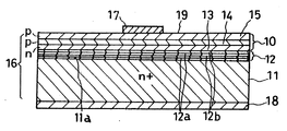
図1及び図2に示す本発明の実施形態に従う青色レ−ザダイオードは、発光機能を得るための複数の窒化ガリウム系化合物半導体層から成る半導体領域10と、シリコン半導体から成るサブストレート即ち基板11と、バッファ層12とを有している。発光機能を有する半導体領域10は、GaN(窒化ガリウム)から成る第1の半導体層としてのn形半導体層13、p形のInGaN(窒化ガリウム インジウム)から成る活性層14、及び第2の半導体層としてのGaN(窒化ガリウム)から成るp形半導体層15とから成る。基板11とバッファ層12と発光機能を有する半導体領域10との積層体から成る基体16の一方の主面(上面)即ちp形半導体層15の表面上に第1の電極としてのアノード電極17が配置され、この基体16の他方の主面(下面)即ち基板11の他方の主面に第2の電極としてのカソード電極18が配置されている。バッファ層12、n形半導体層13、活性層14、及びp形半導体層15は、基板11の上に順次にそれぞれの結晶方位を揃えてエピタキシャル成長させたものである。
【0010】
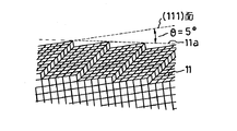
基板11は、導電形決定不純物としてAs(砒素)を含むn+形シリコン単結晶から成る。このシリコン基板11は低指数結晶面から小さな角度で傾斜させた表面を有するオフオリエンテ−ション基板である。具体的には、図3及び図5(A)に示すように基板11のバッファ層12が配置される側の主面11aは、ミラ−指数で示す結晶の面方位において(111)面から[11-0]方向に約5度傾斜させた面である。ここで1-は既に説明したよう1の反転を示す。従って、基板11の一方の主面11aは図3に概略的に示すように多数のステップとテラスとが交互に形成された表面(以下「多段ステップ面」という)を構成している。また、この基板11の不純物濃度は、5×1018cm-3〜5×1019cm-3程度であり、この基板11の抵抗率は0.0001Ω・cm〜0.01Ω・cm程度である。抵抗率が比較的低い基板11はアノ−ド電極17とカソード電極18との間の電流通路として機能する。また、基板11は、比較的厚い約350μmの厚みを有し、p形半導体層15、活性層14及びn形半導体層13から成る発光機能を有する半導体領域10及びバッファ層12の支持体として機能する。
【0011】
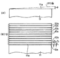
基板11の一方の主面全体を被覆するように配置されたバッファ層12は、複数の第1の層12aと複数の第2の層12bとが交互に積層された複合層から成る。図1及び図2では、図示の都合上、バッファ層12が2つの第1の層12aと2つの第2の層12bとで示されているが、
実際には、バッファ層12は、10個の第1の層12aと10個の第2の層12bとを有する。
【0012】
第1の層12aは、
化学式 AlxGa1-xN
ここで、xは0<x≦1を満足する任意の数値、
で示すことができる材料で形成される。即ち、第1の層12aは、AlN(窒化アルミニウム)又はAlGaN(窒化ガリウム アルミニウム)で形成される。図1及び図2の実施形態では、前記式のxが1とされた材料に相当するAlN(窒化アルミニウム)が第1の層12aに使用されている。第1の層12aは、絶縁性を有する極薄い膜である。第1の層12aの格子定数及び熱膨張係数は第2の層12bよりもシリコン基板11に近い。従って、第1の層11aは第2の層12bよりもバッファ作用が大きい。
【0013】
第2の層12bは、GaN(窒化ガリウム)又は
化学式AlyGa1-yN
ここで、yは、y<x及び0<y<1を満足する任意の数値、で示すことができる材料から成るn形半導体の極く薄い膜である。第2の層12bとしてAlyGa1-yNから成るn形半導体を使用する場合には、第2の層12bの電気抵抗の増大を抑えるために、yを0<y<0.8を満足する値即ち0よりも大きく且つ0.8よりも小さくすることが望ましい。第2の層12bは第1の層12aの電気的接続導電体又は半導体として機能する。
【0014】
バッファ層12の第1の層12aの厚みは、好ましくは0.5nm〜10nm即ち5〜100オングストロ−ム、より好ましくは1nm〜8nmである。第1の層12aの厚みが0.5nm未満の場合にはバッファ層12の上面に形成されるn形半導体領域13の結晶性が良好に保てなくなる。第1の層12aの厚みが10nmを超えると、量子力学的トンネル効果を良好に得ることができなくなり、バッファ層12の電気的抵抗が増大する。
【0015】
第2の層12bの厚みは、好ましくは5nm〜2000nm即ち50〜20000オングストロ−ムであり、より好ましくは10nm〜300nmである。第2の層12bの厚みが10nm未満の場合には、基板11と第2の層12bとの間のエネルギバンドの不連続性が比較的大きくなり、発光素子の動作時のアノード電極17とカソード電極18との間の抵抗及び電圧Vfが比較的大きくなる。また、第2の層12bの厚みが10nm未満の場合には、第2の層12bの上に形成される一方の第1の層11aと第2の層12bの下に形成される他方の第1の層11aとの間の電気的接続が良好に達成されず、バッファ層12の電気的抵抗が増大する。第2の層12bの厚みが300nmを超えた場合には、バッファ層12全体に対する第1の層11aの割合が低下し、バッファ機能が相対的に小さくなり、半導体領域10の結晶性が良好に保てなくなる。
【0016】
バッファ層12を構成する第1の層12aと第2の層12bは、いずれも基板11の一方の主面11aの表面状態を引き継いで形成される。このため、第1の層12a及び第2の層12bの表面は、多数のステップとテラスとが交互に形成された表面(以下「多段ステップ面」という)を構成している。結果として、バッファ層12の一方の主面は、基板11の一方の主面と同じ多段ステップ面となっている。ただし、バッファ層12の一方の主面におけるテラスの幅は、シリコン基板11の一方の主面におけるテラスの幅よりも小さいこともある。
【0017】
バッファ層12の一方の主面には、厚み約0.2μmのn形GaNから成るn形半導体層13が形成されている。このn形半導体層13は、バッファ層12の一方の主面の表面状態を引き継いで形成されるため、その一方の主面は多数のステップとテラスとが交互に形成された表面(以下「多段ステップ面」という)を構成している。
【0018】
n形半導体層13の一方の主面には、厚み約2nm即ち20オングストロ−ムのp形InGaNから成る活性層14が形成されている。この活性層14はn形半導体層13の一方の主面の表面状態を引き継いで形成されるため、その一方の主面は多数のステップとテラスとが交互に形成された表面(以下「多段ステップ面」という)を構成している。この結果、膜厚が2nm程度の薄い活性層14では、ステップ端を利用した多数の量子細線は形成されている。
【0019】
活性層14の一方の主面には、厚み約0.2μmのp形GaNから成るp形半導体層15が形成されている。このp形半導体層15も、活性層14の一方の主面の表面状態を引き継いで形成されるため、その一方の主面には多数のステップとテラスとが交互に形成された表面(以下「多段ステップ面」という)を構成している。
【0020】
次に、図1の半導体発光の製造方法について説明する。
まず、図5(A)に示すn形不純物が導入されたn+形シリコン半導体から成る基板11を用意する。量子細線を形成するための基板11の一方の主面は、ミラ−指数で示す結晶の面方位において(111)面から[11-0]方向に5度傾斜させた面となっている。従って、基板11の一方の主面11aは、多段ステップ面となっている。
【0021】
次に、図5(B)に示すように基板11の主面11a上にバッファ層12を形成する。このバッファ層12は、周知のMOCVD(Metal Organic Chemical Vapor Deposition)即ち有機金属化学気相成長法によってAlNから成る第1の層12aとGaNから成る第2の層12bとを繰返して積層することによって形成する。即ち、シリコン単結晶の基板11をMOCVD装置の反応室内に配置し、まず、サーマルアニーリングを施して表面の酸化膜を除去する。次に、反応室内にTMA(トリメチルアルミニウム)ガスとNH3 (アンモニア)ガスを約24秒間供給して、基板11の一方の主面に厚さ約5nmのAlN層から成る第1の層12aを形成する。本実施例では基板11の加熱温度を1120℃とした後に、TMAガスの流量即ちAlの供給量を約63μmol/min、NH3 ガスの流量即ちNH3 の供給量を約0.14mol/minとした。続いて、基板11の加熱温度を1120℃とし、TMAガスの供給を止めてから反応室内にTMG(トリメチルガリウム)ガスとNH3 (アンモニア)ガスとSiH4 (シラン)ガスを約83秒間供給して、基板11の一方の主面に形成された上記AlNから成る第1の層12aの上面に、厚さ約30nmのn形のGaNから成る第2の層12bを形成する。ここで、SiH4ガスは形成膜中にn形不純物としてのSiを導入するためのものである。本実施例では、TMGガスの流量即ちGaの供給量を約63μmol/min、NH3 ガスの流量即ちNH3 の供給量を約0.14mol/min、SiH4 ガスの流量即ちSiの供給量を約21nmol/minとした。本実施例では、上述のAlNから成る第1の層12aとGaNから成る第2の層12bの形成を10回繰り返してAlNから成る第1の層12aとGaNから成る第2の層12bとが交互に20層積層されたバッファ層12を形成する。勿論AlNから成る第1の層12a、GaNから成る第2の層12bをそれぞれ50層等の任意の数に変えることもできる。第1の層12aと第2の層12bは、基板11の一方の主面の表面状態を引き継いで膜成長するため、バッファ層12の一方の主面は多段ステップ面となっている。
【0022】
次に、バッファ層12の上面に周知のMOCVD法によってn形半導体層13、活性層14及びp形半導体層15を順次連続して形成する。
即ち、上面にバッファ層12が形成された基板11をMOCVD装置の反応室内に配置して、反応室内にまずトリメチルガリウムガス即ちTMGガス、NH3 (アンモニア)ガス、SiH4 (シラン)ガスを供給してバッファ層12の上面にn形半導体領域13を形成する。ここで、シランガスはn形半導体層13中にn形不純物としてのSiを導入するためのものである。本実施例ではバッファ層12が形成された基板11の加熱温度を1040℃とした後、TMGガスの流量即ちGaの供給量を約4.3μmol /min、NH3 ガスの流量即ちNH3 の供給量を約53.6mmol /min、シランガスの流量即ちSiの供給量を約1.5nmol /minとした。また、本実施例では、n形半導体層13の厚みを約0.2μmとした。従来の一般的発光ダイオードの場合には、n形半導体層の厚みが約4.0〜5.0μmであるから、これに比べて図1の本実施例のn形半導体層13はかなり肉薄に形成されている。また、n形半導体層13の不純物濃度は約3×1018cm-3であり、基板11の不純物濃度よりは十分に低い。尚、本実施例によればバッファ層12が介在しているので、1040℃のような比較的高い温度でn形半導体層13を形成することが可能になる。このn形半導体層13もバッファ層12の一方の主面状態を受け継いで膜成長するため、その一方の主面は多段ステップ面となっている。
【0023】
続いて、基板11の加熱温度を800℃とし、反応室内にTMGガス、アンモニアガスに加えてトリメチルインジウムガス(以下、TMIガスという)とビスシクロペンタジェニルマグネシウムガス(以下、Cp2 Mgガスという。)を供給してn形半導体層13の上面にp形InGaN(窒化インジウム ガリウム)から成る活性層14を形成する。ここで、Cp2 Mgガスは活性層14中にp形導電形の不純物としてのMg(マグネシウム)を導入するためのものである。本実施例では、TMGガスの流量を約1.1μmol /min、NH3ガスの流量を約67mmol /min、TMIガスの流量即ちInの供給量を約4.5μmol /min、Gp2 Mgガスの流量即ちMgの供給量を約12nmol /minとした。また、活性層14の厚みは約2nm即ち20オングストロ−ムとした。なお、活性層14の不純物濃度は約3×1017cm-3である。活性層14は、この下側のn形半導体層13又はバッファ層12を介して基板11の一方の主面の表面状態を引き継いで形成される。このため、活性層14の一方の主面は、多数のステップと多数のテラスとが交互に形成された多段ステップ面を構成している。
【0024】
続いて、基板11の加熱温度を1040℃とし、反応室内にTMGガス、アンモニアガス及びCp2 Mgガスを供給して活性層14の上面にp形GaN(窒化ガリウム)から成るp形半導体層15を形成する。本実施例では、この時のTMGガスの流量を約4.3μmol /min、アンモニアガスの流量を約53.6μmol /min、Cp2 Mgガスの流量を約0.12μmol /minとした。また、p形半導体層15の厚みは約0.2μmとした。なお、p形半導体層15の不純物濃度は約3×1018cm-3である。このp形半導体層15の一方の主面も多段ステップ面となる。
【0025】
上記のMOCVD成長方法によれば、シリコン単結晶から成る基板11の結晶方位を良好に引き継いでいるバッファ層12を形成することができる。また、バッファ層12の結晶方位に対してn形半導体層13、活性層14及びp形半導体層15の結晶方位を揃えることができる。この結果、良好な結晶性を有し、且つ基板11の多段ステップ面を良好に引き継いだn形半導体13、活性層14及びp形半導体層15が得られる。
【0026】
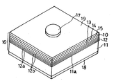
第1の電極としてのアノード電極17は、例えばニッケルと金を周知の真空蒸着法等によって半導体基体16の上面即ちp形半導体層15の上面に付着させることによって形成し、p形半導体層15の表面に低抵抗接触させる。このアノード電極17は図2に示すように円形の平面形状を有しており、半導体基体16の上面のほぼ中央に配置されている。半導体基体16の上面のうち、アノード電極17の形成されていない領域19は、光取り出し領域として機能する。
【0027】
第2の電極としてのカソード電極18は、n形半導体層13に形成せずに、例えばチタンとアルミニウムを周知の真空蒸着法等によって基板11の下面全体に形成する。
【0028】
図1の青色発光ダイオードを外部装置に取付ける時には、例えばカソード電極18を回路基板等の外部電極に対して半田又は導電性接着剤で固着し、アノード電極17を周知のワイヤボンディング方法によって外部電極に対してワイヤで電気的に接続する。
【0029】
本実施形態の青色レ−ザダイオードによれば、次の効果が得られる。
(1) 基板11の一方の主面に形成された格子定数がシリコンとGaNとの間の値を有するAlNから成る第1の層12aは、シリコンから成る基板11の結晶方位を良好に引き継ぐことができる。この結果、バッファ層12の一方の主面に、n形半導体層13、活性層14及びp形半導体層15からなるGaN系半導体領域10を結晶方位を揃えて良好に形成することができる。このため、GaN系半導体領域10の特性が良くなり、発光特性も良くなる。また、GaN系半導体領域10はオフ基板11のステップ表面を引き継ぐので多段ステップなり、量子細線を容易且つ良好に得ることができ、低しきい値のレ−ザダイオ−ドを容易に得ることができる。
(2) 第1の層12aと第2の層12bが複数積層されて成るバッファ層12を介して半導体領域10を形成すると、半導体領域10の結晶性が良くなる。即ち、シリコンから成る基板11の一方の主面に、もしGaN半導体層のみによって構成されたバッファ層を形成した場合、シリコンとGaNとは格子定数の差が大きいため、このバッファ層の上面に結晶性に優れたGaN系半導体領域を形成することはできない。また、比較的厚いAlNのみでバッファ層を形成すると、バッファ層の抵抗が大きくなる。また、比較的薄いAlNのみでバッファ層を形成すると、十分なバッファ機能が得られない。これに対し、本実施例では、基板11とGaN系半導体領域10との間にシリコンとの格子定数差が比較的小さいAlNから成る複数の第1の層12aが介在し、且つ第1の層12aの相互間に第2の層12bが介在した複合構造のバッファ層12が設けられている。このため、バッファ層12の上に結晶性の良いGaN系半導体領域10を形成することができる。この結果、GaN系半導体領域10の発光特性が良くなる。
(3) バッファ層12に含まれている複数の第1の層12aのそれぞれが量子力学的なトンネル効果の生じる厚さに設定されているので、バッファ層12の抵抗の増大を抑えることができる。
(4) 基板11とGaN系半導体領域10との熱膨張係数の差に起因する歪みの発生を抑制できる。即ち、シリコンの熱膨張係数とGaNの熱膨張係数とは大きく相違するため、両者を直接に積層すると熱膨張係数差に起因する歪みが発生し易い。しかし、本実施例のAlNからなる第1の層12aの熱膨張係数は基板11の熱膨張係数とGaN系半導体領域10の熱膨張係数との中間値を有する。また。第1の層12aと第2の層12bとの複合層から成るバッファ層12の平均的な熱膨張係数は基板11の熱膨張係数とGaN系半導体領域10の熱膨張係数との中間値を有する。このため、このバッファ層12によって基板11とGaN半導体領域10との熱膨張係数の差に起因する歪みの発生を抑制することができる。
【0030】
【変形例】
本発明は上述の実施形態に限定されるものでなく、例えば次の変形が可能なものである。
(1) 半導体基体16の各層の導電形を実施例と逆にすることができる。
(2) n形半導体層13、活性層14及びp形半導層15のそれぞれを、複数の半導体層の組み合せで構成することができる。
(3) n形半導体層13、活性層14及びp形半導層15のそれぞれの材料を、GaN(窒化ガリウム)、AlInN(窒化インジウム アルミニウム)、AlGaN(窒化ガリウム アルミニウム)、InGaN(窒化ガリウム インジウム)、及びAlInGaN(窒化ガリウム インジウム アルミニウム)から選択された窒化ガリウム系化合物半導体又は窒化インジウム系化合物半導体とすることができる。
(4) n形半導体層13を省いてバッファ層12の上にGaInNから成る活性層14を直接に接触させることができる。これにより、肉厚のAlGaNクラッド層を介在させて活性層14を形成する場合に比較して活性層14に加わる引っ張り応力が緩和される。このため、活性層14の結晶性が良好となり、発光素子の発光特性が更に良好に得られる。
(5) アノ−ド電極17の下にオ−ミックコンタクトのためのP+形半導体領域即ちコンタクト層を設けることができる。また、p形半導体領域15とアノ−ド電極17との間に周知の電流拡散層、電流ブロック層を設けることができる。
(6) アノ−ド電極17を透明電極とパット電極との組み合せとで構成することができる。
(7) バッファ層12の第1の層12aの数を第2の層12bよりも1層多くしてバッファ層12の最上層を第1の層12aとすることができる。また、逆に第2の層12bの数を第1の層12aの数よりも1層多くすることもできる。
(8) 第1の層12a及び第2の層12bは、これらの機能を阻害しない範囲で不純物を含むものであってもよい。
(9) 基板11を、単結晶シリコン以外の多結晶シリコン又はSiC等のシリコン化合物とすることができる。
【図面の簡単な説明】
【図1】本発明の1実施形態に従うのレ−ザダイオードを示す中央縦断面図である。
【図2】図1のレ−ザダイオードの斜視図である。
【図3】図1の基板の表面を拡大して概略的に示す斜視図である。
【図4】図2の一部を拡大して量子細線を概略的に示す斜視図である。
【図5】図1のレ−ザダイオ−ドの構造を製造工程順に拡大して示す断面図である。
【符号の説明】
10 GaN系半導体領域
11 シリコン単結晶から成る基板
12 バッファ層
12a AlNから成る第1の層
12b GaNから成る第2の層
13 n形半導体層
14 活性層
15 p形半導体層
16 基体
18 アノード電極
19 カソード電極[0001]
BACKGROUND OF THE INVENTION
The present invention relates to a method for manufacturing a semiconductor light emitting device having a quantum wire structure.
[0002]
[Prior art]
In recent years, vigorous attempts have been made to manufacture low threshold semiconductor lasers and the like using compound semiconductor quantum wires (linear crystals of several tens of nanometers). For example, Journal of Applied Physics, Vol. 67, No. 7, pp. 776-785, on a GaAs semiconductor substrate having a substrate structure having a surface tilted from the plane orientation of the crystal indicated by the Miller index with several degrees of off-substrate. An infrared laser in which an InGaAs-based quantum wire is formed is disclosed. According to the technique described in this document, a quantum wire can be formed on the multi-step atomic step surface of the material on the surface of the substrate using a self-organization mechanism, so that a semiconductor light emitting device having a quantum wire structure can be easily manufactured. it can. In other words, quantum wires can be formed using atomic steps (steps on the atomic plane of the crystal surface) formed on the substrate surface. Compared to the conventional method of forming quantum wires using photolithography and etching. Thus, there is an advantage that a semiconductor laser having a quantum wire structure can be manufactured with high productivity.
[0003]
[Problems to be Solved by the Invention]
However, in order to manufacture a semiconductor light emitting device having a light emitting functional layer made of a nitride compound semiconductor, it is necessary to grow a nitride compound semiconductor region on a substrate material made of sapphire. In order to grow a nitride compound semiconductor region on a sapphire substrate, an amorphous low-temperature buffer layer is generally formed on the sapphire substrate, and the light-emitting functional layer is formed through this buffer layer. Compound semiconductor area
Form.
[0004]
By the way, this amorphous layer is crystallized during the temperature rise, and the nitride compound semiconductor layer formed on the amorphous layer is grown by inheriting the crystal orientation of the crystallized buffer layer. In other words, the orientation and crystallinity of the nitride-based compound semiconductor layer to be stacked are more greatly affected by the orientation and crystallinity of the island-like crystal where the amorphous layer is crystallized at a higher temperature than the influence of the sapphire substrate. For this reason, even if an off-substrate is used like the above-described InGaAs-based quantum wires, the crystal orientation of the low-temperature buffer layer is inherited, so that it is difficult to form quantum wires using a self-organization mechanism.
[0005]
Accordingly, an object of the present invention is to provide a method for manufacturing a nitride-based compound semiconductor device having a quantum wire structure using a self-organizing mechanism.
[0006]
[Means for Solving the Problems]
In order to solve the above problems and achieve the above object, the present invention provides:
One main surface is [11] from the (111) plane of the crystal plane orientation indicated by the Miller index.-0] direction or [1-10] direction or [1-1-2] direction or [112-Preparing a silicon substrate tilted at an angle of 0.5 to 5 degrees in any of the directions;
On one main surface of the silicon substrate,
Chemical formula AlxGa1-xN
Where x is 0 <x ≦ 1
Satisfying the numerical value,
A step of vapor-phase-growing a material that can be represented by a thickness of 0.5 to 10 nm to obtain a first buffer layer (
On the first buffer layer
GaN or chemical formula AlyGa1-yN
Where y is y <x
0 <y <1
Satisfying the numerical value,
A step of obtaining a second buffer layer (
On the second buffer layerWith quantum wiresA step of forming a plurality of nitride compound semiconductor layers for obtaining a light emitting function by a vapor deposition method;
The present invention relates to a method for manufacturing a semiconductor light emitting device.
In the present invention, in order to simplify the notation of the crystal plane orientation indicated by the Miller index, the inversion of 1 is 1-, 2 inversion 2-I will show in
[0007]
【The invention's effect】
The present inventionHas the following effects:.
(A) From the (111) plane of one of the principal planes indicated by the Miller index, [11] - 0] direction or [1 - 10] direction or [1 - 1 - 2] direction or [112 - ] A silicon substrate inclined at an angle of 0.5 to 5 degrees in any of the directions has the chemical formula Al x Ga 1-x A material that can be represented by N is vapor-grown to a thickness of 0.5 to 10 nm to obtain a first buffer layer, and then GaN or the chemical formula Al y Ga 1-y A material that can be represented by N is vapor-grown to a thickness of 10 to 300 nm to obtain a second buffer layer, and thenA plurality of nitride compound semiconductor layers having a light emitting function are formed. For this reason,siliconA buffer layer and a light emitting functional semiconductor layer that inherit the crystal orientation of the substrate are obtained. That is,siliconSince the board is an off-orientation board,siliconThe surface of the substrate has atomic steps, and the buffer layer and the light emitting functional semiconductor layer also have atomic steps, and quantum wires are generated. As a result, a light emitting functional semiconductor layer having a quantum wire can be formed easily and satisfactorily.
(B) When the light emitting functional semiconductor layer is formed through the buffer layer formed by stacking the first buffer layer and the second buffer layer, the crystallinity of the light emitting functional semiconductor layer is improved..
(C) Since the first buffer layer is formed with a thickness of 0.5 to 10 nm, a quantum mechanical tunnel effect can be obtained. Thereby, an increase in the resistance of the buffer layer can be suppressed..
(D) It is possible to suppress the occurrence of distortion due to the difference in thermal expansion coefficient between the silicon substrate and the light emitting functional semiconductor layer made of a nitride compound semiconductor. That is, since the thermal expansion coefficient of silicon and the thermal expansion coefficient of the nitride compound semiconductor are greatly different from each other, if the two are directly laminated, distortion due to the difference in thermal expansion coefficient is likely to occur. However, the first buffer layer is Al x Ga 1-x N, where x is a material that can be expressed by a numerical value satisfying 0 <x ≦ 1, and the thermal expansion coefficient of the first buffer layer is the thermal expansion coefficient of the silicon substrate and the thermal expansion of the light emitting functional semiconductor layer. It has an intermediate value with the coefficient. The average thermal expansion coefficient of the buffer layer composed of the composite layer of the first buffer layer and the second buffer layer has an intermediate value between the thermal expansion coefficient of the silicon substrate and the thermal expansion coefficient of the light emitting functional semiconductor layer. . For this reason, the first and second buffer layers can suppress the occurrence of distortion due to the difference in thermal expansion coefficient between the silicon substrate and the light emitting functional semiconductor layer..
[0008]
[First Embodiment]
Next, a gallium nitride compound blue laser diode as a Group 3-5 compound semiconductor light emitting device according to an embodiment of the present invention will be described with reference to FIGS.
[0009]
The blue laser diode according to the embodiment of the present invention shown in FIGS. 1 and 2 includes a
[0010]
The
[0011]
The
Actually, the
[0012]
The
Chemical formula AlxGa1-xN
Here, x is an arbitrary numerical value satisfying 0 <x ≦ 1,
It is formed with the material which can be shown by. That is, the
[0013]
The
Chemical formula AlyGa1-yN
Here, y is a very thin film of an n-type semiconductor made of a material that can be expressed by any numerical value satisfying y <x and 0 <y <1. Al as the
[0014]
The thickness of the
[0015]
The thickness of the
[0016]
The
[0017]
An n-
[0018]
An
[0019]
A p-
[0020]
Next, a method for manufacturing the semiconductor light emission of FIG. 1 will be described.
First, n into which an n-type impurity shown in FIG.+A substrate 11 made of a silicon semiconductor is prepared. One main surface of the
[0021]
Next, as shown in FIG. 5B, the
[0022]
Next, the n-
That is, the
[0023]
Subsequently, the heating temperature of the
[0024]
Subsequently, the heating temperature of the
[0025]
According to the MOCVD growth method described above, the
[0026]
The
[0027]
The
[0028]
When the blue light emitting diode of FIG. 1 is attached to an external device, for example, the
[0029]
According to the blue laser diode of this embodiment, the following effects can be obtained.
(1) The
(2) When the
(3) Since each of the plurality of
(4) Generation of strain due to the difference in thermal expansion coefficient between the
[0030]
[Modification]
The present invention is not limited to the above-described embodiment, and for example, the following modifications are possible.
(1) The conductivity type of each layer of the
(2) Each of the n-
(3) The materials of the n-
(4) The n-
(5) P for ohmic contact under the anode electrode 17+A shaped semiconductor region or contact layer may be provided. In addition, a known current diffusion layer and current blocking layer can be provided between the p-
(6) The
(7) The number of
(8) The
(9) The
[Brief description of the drawings]
FIG. 1 is a central longitudinal sectional view showing a laser diode according to an embodiment of the present invention.
2 is a perspective view of the laser diode of FIG. 1. FIG.
3 is an enlarged perspective view schematically showing a surface of the substrate of FIG. 1; FIG.
4 is a perspective view schematically showing a quantum wire by enlarging a part of FIG. 2; FIG.
5 is a sectional view showing the structure of the laser diode in FIG.
[Explanation of symbols]
10 GaN-based semiconductor region
11 Substrate made of silicon single crystal
12 Buffer layer
12a First layer of AlN
12b Second layer of GaN
13 n-type semiconductor layer
14 Active layer
15 p-type semiconductor layer
16 Base
18 Anode electrode
19 Cathode electrode
Claims (1)
前記シリコン基板の一方の主面に、
化学式 AlxGa1-xN
ここでxは、0<x≦1
を満足する数値、
で示すことができる材料を0.5〜10nmの厚みに気相成長させて第1のバッファ層を得る工程と、
前記第1のバッファ層の上に
GaN又は化学式 AlyGa1-yN
ここで、yは、y<x
0<y<1
を満足する数値、
で示すことができる材料を10〜300nmの厚みに気相成長させて第2のバッファ層を得る工程と、
前記第2のバッファ層の上に量子細線を有する発光機能を得るための複数の窒化物系化合物半導体層を気相成長法によって形成する工程と
を有していることを特徴とする半導体発光素子の製造方法。One principal mirror - the crystal plane orientation indicated by an index (111) plane from the [11 - 0] direction or the [1 - 10] direction or [11 - 2] direction or the [112 -] direction either Preparing a silicon substrate inclined at an angle of 0.5 to 5 degrees;
On one main surface of the silicon substrate,
Chemical formula Al x Ga 1-x N
Where x is 0 <x ≦ 1
Satisfying the numerical value,
A step of vapor-depositing a material that can be represented by a thickness of 0.5 to 10 nm to obtain a first buffer layer;
GaN or chemical formula Al y Ga 1-y N on the first buffer layer
Where y is y <x
0 <y <1
Satisfying the numerical value,
A step of vapor-phase-growing a material that can be represented by a thickness of 10 to 300 nm to obtain a second buffer layer;
And a step of forming a plurality of nitride-based compound semiconductor layers on the second buffer layer by a vapor deposition method for obtaining a light emitting function having a quantum wire. Manufacturing method.
Priority Applications (1)
| Application Number | Priority Date | Filing Date | Title |
|---|---|---|---|
| JP2001386428A JP4041908B2 (en) | 2001-12-19 | 2001-12-19 | Manufacturing method of semiconductor light emitting device |
Applications Claiming Priority (1)
| Application Number | Priority Date | Filing Date | Title |
|---|---|---|---|
| JP2001386428A JP4041908B2 (en) | 2001-12-19 | 2001-12-19 | Manufacturing method of semiconductor light emitting device |
Publications (2)
| Publication Number | Publication Date |
|---|---|
| JP2003188414A JP2003188414A (en) | 2003-07-04 |
| JP4041908B2 true JP4041908B2 (en) | 2008-02-06 |
Family
ID=27595584
Family Applications (1)
| Application Number | Title | Priority Date | Filing Date |
|---|---|---|---|
| JP2001386428A Expired - Lifetime JP4041908B2 (en) | 2001-12-19 | 2001-12-19 | Manufacturing method of semiconductor light emitting device |
Country Status (1)
| Country | Link |
|---|---|
| JP (1) | JP4041908B2 (en) |
Cited By (1)
| Publication number | Priority date | Publication date | Assignee | Title |
|---|---|---|---|---|
| US8957432B2 (en) | 2010-04-28 | 2015-02-17 | Samsung Electronics Co., Ltd. | Semiconductor device |
Families Citing this family (8)
| Publication number | Priority date | Publication date | Assignee | Title |
|---|---|---|---|---|
| SG170031A1 (en) * | 2006-02-23 | 2011-04-29 | Azzurro Semiconductors Ag | Nitride semiconductor component and process for its production |
| KR20090040357A (en) * | 2006-09-29 | 2009-04-23 | 쇼와 덴코 가부시키가이샤 | Formation method of group III nitride compound semiconductor laminate |
| JP4974635B2 (en) * | 2006-10-06 | 2012-07-11 | 昭和電工株式会社 | Film forming method of group III nitride compound semiconductor multilayer structure |
| JP2008098245A (en) * | 2006-10-06 | 2008-04-24 | Showa Denko Kk | Film forming method of group iii nitride compound semiconductor laminate structure |
| JP2008091470A (en) * | 2006-09-29 | 2008-04-17 | Showa Denko Kk | Film forming method of group III nitride compound semiconductor multilayer structure |
| JP5133927B2 (en) * | 2009-03-26 | 2013-01-30 | コバレントマテリアル株式会社 | Compound semiconductor substrate |
| CN114744088A (en) * | 2022-03-11 | 2022-07-12 | 南昌大学 | Graphical deflection angle silicon substrate and preparation method thereof |
| JP7626834B1 (en) | 2023-12-27 | 2025-02-04 | 日機装株式会社 | Nitride semiconductor light emitting device |
-
2001
- 2001-12-19 JP JP2001386428A patent/JP4041908B2/en not_active Expired - Lifetime
Cited By (1)
| Publication number | Priority date | Publication date | Assignee | Title |
|---|---|---|---|---|
| US8957432B2 (en) | 2010-04-28 | 2015-02-17 | Samsung Electronics Co., Ltd. | Semiconductor device |
Also Published As
| Publication number | Publication date |
|---|---|
| JP2003188414A (en) | 2003-07-04 |
Similar Documents
| Publication | Publication Date | Title |
|---|---|---|
| US6611004B2 (en) | Gallium nitride based light emitting element | |
| US7176480B2 (en) | Light-emitting semiconductor device having a quantum well active layer, and method of fabrication | |
| CN102308370B (en) | Epitaxial wafer, method for manufacturing gallium nitride-based semiconductor device, gallium nitride-based semiconductor device, and gallium oxide wafer | |
| CN1846310B (en) | Nitride semiconductor device and manufacturing method thereof | |
| JP4210823B2 (en) | Shiyaki barrier diode and manufacturing method thereof | |
| JP3500281B2 (en) | Gallium nitride based semiconductor device and method of manufacturing the same | |
| JPWO2011010436A1 (en) | Light emitting diode | |
| CN101689586A (en) | Nitride semiconductor light emitting element and method for manufacturing nitride semiconductor | |
| TW201041181A (en) | Gallium nitride-based semiconductor optical device, method of manufacturing gallium nitride-based semiconductor optical device, and epitaxial wafer | |
| JP5579435B2 (en) | Nitride-based semiconductor device and manufacturing method thereof | |
| JP3233139B2 (en) | Nitride semiconductor light emitting device and method of manufacturing the same | |
| JP4058595B2 (en) | Semiconductor light emitting device and manufacturing method thereof | |
| JP4041908B2 (en) | Manufacturing method of semiconductor light emitting device | |
| JP2005183930A (en) | Semiconductor light emitting element and its manufacturing method | |
| JP4058590B2 (en) | Semiconductor light emitting device | |
| JP2010272593A (en) | Nitride semiconductor light emitting element and manufacturing method of the same | |
| JP3981797B2 (en) | Semiconductor light emitting device | |
| JP2001015852A (en) | Electrode structure on p-type group III nitride semiconductor layer and method of forming the same | |
| KR100475005B1 (en) | Nitride semiconductor device | |
| JP4058592B2 (en) | Semiconductor light emitting device and manufacturing method thereof | |
| JP2001313421A (en) | Semiconductor light-emitting element and its manufacturing method | |
| JP4255168B2 (en) | Nitride semiconductor manufacturing method and light emitting device | |
| JPH11330622A (en) | Nitride semiconductor device | |
| JP4058593B2 (en) | Semiconductor light emitting device | |
| JP4058594B2 (en) | Semiconductor light emitting device |
Legal Events
| Date | Code | Title | Description |
|---|---|---|---|
| A711 | Notification of change in applicant |
Free format text: JAPANESE INTERMEDIATE CODE: A712 Effective date: 20040928 |
|
| RD02 | Notification of acceptance of power of attorney |
Free format text: JAPANESE INTERMEDIATE CODE: A7422 Effective date: 20041018 |
|
| A621 | Written request for application examination |
Free format text: JAPANESE INTERMEDIATE CODE: A621 Effective date: 20041020 |
|
| A521 | Request for written amendment filed |
Free format text: JAPANESE INTERMEDIATE CODE: A821 Effective date: 20041018 |
|
| A977 | Report on retrieval |
Free format text: JAPANESE INTERMEDIATE CODE: A971007 Effective date: 20070409 |
|
| A131 | Notification of reasons for refusal |
Free format text: JAPANESE INTERMEDIATE CODE: A131 Effective date: 20070418 |
|
| A521 | Request for written amendment filed |
Free format text: JAPANESE INTERMEDIATE CODE: A523 Effective date: 20070618 |
|
| A521 | Request for written amendment filed |
Free format text: JAPANESE INTERMEDIATE CODE: A523 Effective date: 20070629 |
|
| A131 | Notification of reasons for refusal |
Free format text: JAPANESE INTERMEDIATE CODE: A131 Effective date: 20070725 |
|
| A521 | Request for written amendment filed |
Free format text: JAPANESE INTERMEDIATE CODE: A523 Effective date: 20070914 |
|
| TRDD | Decision of grant or rejection written | ||
| A01 | Written decision to grant a patent or to grant a registration (utility model) |
Free format text: JAPANESE INTERMEDIATE CODE: A01 Effective date: 20071010 |
|
| A61 | First payment of annual fees (during grant procedure) |
Free format text: JAPANESE INTERMEDIATE CODE: A61 Effective date: 20071025 |
|
| R150 | Certificate of patent or registration of utility model |
Ref document number: 4041908 Country of ref document: JP Free format text: JAPANESE INTERMEDIATE CODE: R150 Free format text: JAPANESE INTERMEDIATE CODE: R150 |
|
| FPAY | Renewal fee payment (event date is renewal date of database) |
Free format text: PAYMENT UNTIL: 20101122 Year of fee payment: 3 |
|
| FPAY | Renewal fee payment (event date is renewal date of database) |
Free format text: PAYMENT UNTIL: 20101122 Year of fee payment: 3 |
|
| FPAY | Renewal fee payment (event date is renewal date of database) |
Free format text: PAYMENT UNTIL: 20101122 Year of fee payment: 3 |
|
| FPAY | Renewal fee payment (event date is renewal date of database) |
Free format text: PAYMENT UNTIL: 20111122 Year of fee payment: 4 |
|
| R250 | Receipt of annual fees |
Free format text: JAPANESE INTERMEDIATE CODE: R250 |
|
| FPAY | Renewal fee payment (event date is renewal date of database) |
Free format text: PAYMENT UNTIL: 20111122 Year of fee payment: 4 |
|
| FPAY | Renewal fee payment (event date is renewal date of database) |
Free format text: PAYMENT UNTIL: 20121122 Year of fee payment: 5 |
|
| R250 | Receipt of annual fees |
Free format text: JAPANESE INTERMEDIATE CODE: R250 |
|
| FPAY | Renewal fee payment (event date is renewal date of database) |
Free format text: PAYMENT UNTIL: 20131122 Year of fee payment: 6 |
|
| R250 | Receipt of annual fees |
Free format text: JAPANESE INTERMEDIATE CODE: R250 |
|
| R250 | Receipt of annual fees |
Free format text: JAPANESE INTERMEDIATE CODE: R250 |
|
| R250 | Receipt of annual fees |
Free format text: JAPANESE INTERMEDIATE CODE: R250 |
|
| R250 | Receipt of annual fees |
Free format text: JAPANESE INTERMEDIATE CODE: R250 |
|
| S111 | Request for change of ownership or part of ownership |
Free format text: JAPANESE INTERMEDIATE CODE: R313117 |
|
| R250 | Receipt of annual fees |
Free format text: JAPANESE INTERMEDIATE CODE: R250 |
|
| R350 | Written notification of registration of transfer |
Free format text: JAPANESE INTERMEDIATE CODE: R350 |
|
| EXPY | Cancellation because of completion of term |