JP4040468B2 - Active switching star node and network of stations interconnected by such star node - Google Patents
Active switching star node and network of stations interconnected by such star node Download PDFInfo
- Publication number
- JP4040468B2 JP4040468B2 JP2002571635A JP2002571635A JP4040468B2 JP 4040468 B2 JP4040468 B2 JP 4040468B2 JP 2002571635 A JP2002571635 A JP 2002571635A JP 2002571635 A JP2002571635 A JP 2002571635A JP 4040468 B2 JP4040468 B2 JP 4040468B2
- Authority
- JP
- Japan
- Prior art keywords
- signal
- terminal
- input
- electronic switch
- star node
- Prior art date
- Legal status (The legal status is an assumption and is not a legal conclusion. Google has not performed a legal analysis and makes no representation as to the accuracy of the status listed.)
- Expired - Fee Related
Links
Images

Classifications
-
- H—ELECTRICITY
- H04—ELECTRIC COMMUNICATION TECHNIQUE
- H04L—TRANSMISSION OF DIGITAL INFORMATION, e.g. TELEGRAPHIC COMMUNICATION
- H04L12/00—Data switching networks
- H04L12/28—Data switching networks characterised by path configuration, e.g. LAN [Local Area Networks] or WAN [Wide Area Networks]
- H04L12/44—Star or tree networks
Landscapes
- Engineering & Computer Science (AREA)
- Computer Networks & Wireless Communication (AREA)
- Signal Processing (AREA)
- Small-Scale Networks (AREA)
Abstract
Description
【0001】
【発明の属する技術分野】
本発明は、ネットワークにおいて複数の局(ST1−ST3)を相互接続するための星形ノード(SN1)であって、上記星形ノード(SN1)はインターフェース(I1−I3)を有し、上記インターフェースは、上記複数の局のうちの選択された局を上記星形ノード(SN1)に接続するための接続端子(BP)を有し、上記インターフェースは上記インターフェースに対応する局からの信号を上記接続端子(BP)において受け取り上記信号を他のインターフェースの接続端子(BP)に送るための手段を有する星形ノード(SN1)に関する。
【0002】
本発明は、斯かる星形ノードによって相互接続される局のネットワークにも関する。この種類のネットワークは、例えば、自動車及び他の騒音のする環境で使用することができる。
【0003】
【従来の技術】
ネットワーク、特に高速ネットワークでは、ネットワークでの反射が信号保全性の問題を起こし得る。この問題は、ビット時間がネットワークを通じた伝播遅延に対して大きくない場合、特に重大である。全ての局が適切に終端した伝送線で星形ノードに接続されているネットワークを作ることができる。斯かる星形タイプのネットワークでは、星形ノードの作業は、局の1つから受け取るデータを他の全ての局に転送することである。斯かる星形タイプのネットワーク及び星形ノードは、米国特許第4,903,015号から既知である。この既知のネットワークは、適切に終端した伝送線を有しており、それ故に、高速に適している。局に送られ局から受け取られる信号は同じ伝送線を流れ、これによって、コネクタ及びワイヤが節約される。しかし、この既知のネットワークの星形ノードでは、送受信の切替機構を実現するために、かなり複雑な論理回路が要求される。論理回路の複雑さは、星形ノードに接続可能な局の数によって増大する。
【0004】
【発明が解決しようとする課題】
本発明の目的は、複雑さが低減された星形ノードを提供することにある。
【0005】
【課題を解決するための手段】
これに対して、本発明によれば、冒頭に規定される星形ノードは、上記星形ノードが共通端子を有し、上記インターフェースが、上記接続端子に結合される入力部を有し上記対応する局からの信号を受け取るための受信器と、上記接続端子に結合される出力部を有する送信器と、上記受信器の入力部における信号遷移に応答して第1の活性信号を生成するための第1の活性検出器と、上記共通端子における信号遷移に応答して第2の活性信号を生成するための第2の活性検出器と、上記第2の活性信号に応答して上記受信器の出力部から上記共通端子への信号転送を禁止するための第1のスイッチング手段と、上記第1の活性信号に応答して上記共通端子から上記送信器の入力部への信号転送を禁止するための第2のスイッチング手段とを有することを特徴とする。
【0006】
第1及び第2のスイッチング手段は、第1及び第2の活性検出器と協働して、インターフェースの対応する局からの入力信号が同一の局に送られることを防止し、入力信号が他の局にのみ送られることを保証する。全てのインターフェースが同一であり、インターフェースの数の増加によって部品の数は増加しない。
【0007】
従属項2の実施例では、インターフェースのドライバ、抵抗器、及び共通端子、は自在に拡張可能なワイヤードORシステムを構成する。電子スイッチは信号の適切なルーティングを提供する。
【0008】
従属項3及び4並びに従属項6及び7の実施例は高速且つ単純なものを提供し、従属項5及び8の実施例は完全に平衡がとれているものである。
【0009】
本発明による星形ノードの単純さは、星形ノードの設定にほとんど時間を奪われないので、高速且つ効率的なデータ伝送を可能にする。それ故に、星形ノードにおいてスイッチング機能を実行する時間を作るための、送信されたデータのプロトコルのプリアンブルは必要でない。これは、本発明による星形ノードが備えられるネットワークを、TTP/C(Time Triggered Protocol Class C(高速≧1Mbit/sec))のようなプリアンブルを規定しないプロトコルに適したものにする。本発明による星形ノードは容易な拡張を更に可能にする。インターフェースの1つを他の星形ノードのインターフェースに接続することによって、星形ノードを加えることができる。
【0010】
本発明のこれら及び他の態様は、添付されている図面を基準にして記載され説明される。これらの図において、同様の構成要素には同様の符号が付されている。
【0011】
【発明の実施の形態】
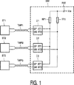
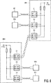
図1は、例として、本発明による星形ノードSN1を通じて相互接続された3つの局ST1、ST2及びST3を有するネットワークを示す。自動車の場合、局は、ネットワークへの接続に適したインターフェースが備えられた温度センサ、ブレーキセンサ、ドアセンサ等とすることができる。星形ノードSN1は、例として、3つのインターフェースI1、I2及びI3を有する。インターフェースI1、I2及びI3は、局ST1、ST2及びST3のうちの対応する局の星形ノードSN1への接続のための接続ターミナルBP及びBMを有する。局ST1、ST2及びST3は、ツイストペア伝送線TWP1、TWP2及びTWP3によってインターフェースI1、I2及びI3に接続されている。しかしながら、同軸ケーブル及び単一ワイヤ線のような、他の種類の伝送線も可能である。局及びインターフェースの数は3つに限られず、2つ以上の任意の数が可能である。
【0012】
インターフェースI1、I2及びI3は、ツイストペア伝送線の接続のための平衡入力部BP及びBMを有し、更に平衡共通端子RT1及びRT2を有する。インターフェースI1、I2及びI3の共通端子RT1は全て、第1の共通プルアップ抵抗RP1を通じて正の供給端子PSTに接続されている。インターフェースI1、I2及びI3の共通端子RT2は全て、第2の共通プルアップ抵抗RP2を通じて正の供給端子PSTに接続されている。
【0013】
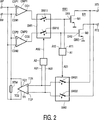
図2は、インターフェースI1−I3のブロック図を示す。インターフェースは、2つの比較器CMP1及びCMP2で構成される受信器と送信器TRとを有する。比較器CMP1は、接続端子BPに接続されている非反転入力部CIP1と、接続端子BMに接続されている反転入力部CIN1とを有する。比較器CMP2は、接続端子BMに接続されている非反転入力部CIP2と、接続端子BPに接続されている反転入力部CIN2とを有する。従って、2つの比較器の入力部は、接続端子に反対に接続されている。送信器TRは、接続端子BM及びBPにそれぞれ接続された平衡出力部TO1及びTO2を有する。終端抵抗RTMは、接続された局のツイストペア伝送線に適正な終端インピーダンスを提供するために、接続端子BPとBMとの間に接続されている。
【0014】
インターフェースは、さらに第1及び第2の信号活性検出器A1及びA2を有する。第1の信号活性検出器A1は入力信号、即ち、インターフェースに接続される局から受信器により受け取られる信号の変化を検出する。第2の活性検出器は、出力信号、即ち、送信器によってインターフェースに接続される局に送信される信号の変化を検出する。
【0015】
2つの比較器CMP1及びCMP2は、それぞれ、第1のスイッチング手段SW1を通じて共通端子RT1及びRT2に結合される出力部CO1及びCO2を有する。第1のスイッチング手段SW1は、第2の活性検出器A2からの第2の活性信号AS2の制御によって、出力部CO1及びCO2から共通端子RT1及びRT2への信号転送を禁止する。第1のスイッチング手段SW1は、通常閉じており第2の活性検出器AS2からの第2の活性信号AS2の命令に従って開く第1及び第2の電子スイッチSW11及びSW12が使用されている。第1及び第2の電子スイッチSW11及びSW12は、それぞれ、出力部CO1及びCO2を、ドライバDRの第1及び第2の駆動入力部DR1及びDR2に接続し、及びドライバDRの第1及び第2の駆動入力部DR1及びDR2から切り離し、このドライバDRは、比較器CMP1及びCMP2の出力部CO1及びCO2により供給される相補的な駆動信号の制御によって、共通端子RT1及びRT2をプルダウン又は解放する。
【0016】
ドライバDRは、第1及び第2のN−チャンネルトランジスタM1及びM2が使用されている。第1のトランジスタM1のチャネルは、第1の共通端子RT1と信号接地としての役割をする負の供給電圧端子GNDとの間に接続されている。第1のトランジスタM1の制御電極又はゲートは駆動入力部DR1として動作する。そのゲートにおいて正の信号を受け取ると、第1のトランジスタM1のチャネルは共通端子RT1と負の供給端子GNDとの間に電流導通経路を形成し、第1のトランジスタM1は第1の共通端子RT1における電圧をグランドレベルに引き込む。第2のトランジスタM2のチャンネルは、第2の共通端子RT2と負の供給電圧端子GNDとの間に接続される。第2のトランジスタM2のゲートは駆動入力部DR2として動作する。そのゲートにおいて正の信号を受け取ると、トランジスタM2のチャンネルは第2の共通端子RT2と負の供給端子GNDとの間に電流導通経路を形成し、第2のトランジスタM2は第2の共通端子RT2における電圧をグランドレベルに引き込む。
【0017】
共通プルアップ抵抗RP1及びRP2並びに各インターフェースI1、I2及びI3の第1及び第2のトランジスタM1及びM2は、インターフェースの間に、簡単なワイヤードOR相互接続システムを構成し、これは、インターフェースの数に依存した個々のインターフェースの電子的設計の増加又は変更を必要すること無く、星形ノードSN1内においてインターフェースを任意の数に簡単に拡張することを可能とする。全てのインターフェースは同じ回路を有する。
【0018】
共通プルアップ抵抗RP1、RP2及び対応するプルダウントランジスタM1、M2の代わりに、比較器CMP1及びCMP2の出力部CO1及びCO2からの平衡信号の制御によって第1の共通端子RT1と第2の共通端子RT2との間にローインピーダンス又はハイインピーダンスを提供することができる他のドライバ段でドライバDRを実現してもよい。
【0019】
送信器TRは、第2のスイッチング手段SW2を通じて、第1の共通端子RT1に結合される反転入力部TINと第2の共通端子RT2に結合される非反転入力部TIPとを有する。第2のスイッチング手段SW2は、第1の活性検出器A1からの第1の活性信号AS1の制御によって、共通端子RT1及びRT2から反転入力部TIN及び非反転入力部TIPへの信号転送を禁止する。第2のスイッチング手段SW2は第1及び第2の電子スイッチSW21及びSW22で実現されており、これらスイッチは通常閉であり、第1の活性検出器A1からの第1の活性信号AS1の命令に従って開く。第2のスイッチング手段SW2の第1及び第2の電子スイッチSW21及びSW22は、第1及び第2の共通端子RT1及びRT2を、送信器TRの反転入力部TIN及び非反転入力部TIPに接続し、及び送信器TRの反転入力部TIN及び非反転入力部TIPから切り離す。
【0020】
第1の活性検出器A1は、入力信号の信号活性を検出する目的で、駆動入力部DR1及びDR2に接続された入力部A11及びA12を有する。この代わりに、これら入力部A11及びA12は、同じ効果を得るために、接続端子BP及びBM又は出力部CO1及びCO2に接続されてもよい。第2の活性検出器A2は、出力信号の信号活性を検出する目的で、送信器TRの反転入力部TIN及び非反転入力部TIPにそれぞれ接続された入力部A21及びA22を有する。この代わりに、これら入力部A21及びA22は、同じ効果を得るために、共通端子RT1及びRT2又は接続端子BP及びBMに接続されてもよい。
【0021】
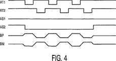
図3は、局からのデータを受け取るインターフェースで生じる信号を示し、上から下に、接続端子BP及びBMにおける相補的なデータ信号、共通端子RT1及びRT2における信号、第1の活性信号AS1、及び第2の活性信号AS2である。図4は、局にデータを送るインターフェースで生じる対応する信号を示す。
【0022】
ネットワークにおいて、データは、データの内容に依存して極性を変える接続端子BPとBMとの間の相補的な電位差として、局から局へと送られる。データが送られないとき、接続端子BPとBMとの間の電圧差はゼロであり、ネットワークはアイドル状態にある。局ST1が送信局であると仮定すると、受け取ったデータ信号のノイズを除去するためにビルトインしきい値を有する2つの比較器CMP1及びCMP2によってインターフェースI1に電圧差が送られる。比較器の出力信号は、通常閉の電子スイッチSW11及びSW12を通じて第1及び第2のトランジスタM1及びM2のゲートを駆動する。第1の活性検出器A1は入力信号の差を検出し、その第1の活性信号AS1で第2のスイッチング手段SW2をすばやく活性化する。これによって、第2のスイッチング手段SW2の第1及び第2の電子スイッチSW21及びSW22が開き、第1及び第2の共通端子RT1及びRT2上の信号は送信器TRの入力部TIN及びTIPから切り離される。信号活性がインターフェースの出力ブランチに存在しないので、電子スイッチSW11及びSW12は閉じたままである。適切な動作のため、第1の活性検出器A1は、共通端子RT1及びRT2からのデータ信号が第2の活性検出器A2の入力部A21及びA22に到達する前に、電子スイッチSW21及びSW22を開かなければならず、このため、入力信号は乱されない。
【0023】
他のインターフェースI2及びI3は接続端子BP及びBMにおいて局からの入力信号を受け取らないが、受信インターフェースI1によって生成される共通端子RT1及びRT2における信号を共有する。他のインターフェースI2及びI3では、第1の活性検出器A1は入力信号の信号差を検出しないので、スイッチSW21及びSW22は閉じる。しかし、共通端子RT1及びRT2における信号差は第1の活性検出器A1によって検出され、これによって、第1及び第2の電子スイッチSW11及びSW12が第2の活性信号AS2に応答して開く。それで、他のインターフェースI2及びI3では、共通端子RT1及びRT2における信号は、送信器TRの入力部TIN及びTIPに接続され、他のインターフェースに接続されている局に送られる。開いたスイッチSW11及びSW12は、共通端子における信号の妨害を防ぐ。適切な動作のために、第2の活性検出器A2は、送信器TRによって送られるデータ信号が第1の活性検出器A1の入力部A11及びA12に到達する前に、電子スイッチSW11及びSW12を開かなければならない。
【0024】
このようにして、局ST1が伝送している限り、局ST1から局ST2及びST3までデータフロー経路が維持される。局ST1がデータの送信を停止すると、インターフェースI1の接続端子BPとBMとの間の電圧差はゼロになり、ネットワークはアイドル状態になる。インターフェースI1では、第1の活性検出器A1は活性の検出を停止し、第2のスイッチング手段SW2の電子スイッチSW21及びSW22は通常閉の位置に戻り、共通端子RT1及びRT2をインターフェースI1の受信器TRの入力部TIN及びTIPに再接続する。ネットワークがアイドル状態にあるので、共通端子RT1及びRT2における信号はアイドル状態を示す高電圧レベルのままである。この結果として、他のインターフェースI2及びI3の電子スイッチSW11及びSW12は通常閉の位置に戻る。全てのインターフェースの中の全てのスイッチは閉じ、星形ノードSN1は、どの局からの新しいデータ信号をも受け取る準備が整う。
【0025】
アイドル状態では、全てのインターフェースの送信器及び受信器はアクティブであり、ネットワークに接続され、全てのデータ経路は完全に開いている。局からのどんなメッセージも、星形ノードSN1によって損失を受けず且つ迅速に中継される。これは、ネットワークを拡張するために星形ノードを縦続接続することが容易であることを意味する。星形ノードSN1の高速動作は、星形ノードの整定時間( settling time )が局の間の相互接続を再配列することを可能にするためのプリアンブルを規定しないプロトコル(例えば 、TTP/C)を使用するネットワークにおいて、星形ノードを適したものにもする。また、フレーム間ギャップをより小さくすることができ、このため、実際のデータの利用可能なバンド幅が増大する。フレーム間ギャップは、1つの送信局から別の送信局への切替えを可能とするために確保されなければならない時間である。この時間は、データ伝送にとって無駄である。
【0026】
活性検出器A1及びA2は、ネットワークがアイドル状態であるとき(即ち、接続端子BPとBMとの間の電圧差がゼロであるとき)ゆっくりと充電され、データが送信されるとき(即ち、電圧差が比較器CMP1及びCMP2によって検出されるとき)素早く放電されるコンデンサから成るようにすることができる。
【0027】
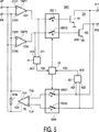
既に述べているように、同じスイッチング効果を得るために、入力部A11及びA12は出力部CO1及びCO2に接続することができ、入力部A21及びA22は、共通端子RT1及びRT2又は接続端子BP及びBMに接続することができる。図5は、この接続構造を有するインターフェースを示す。活性信号AS1及びAS2は、スイッチSW11、SW12、SW21及びSW22を開閉するために駆動信号を供給する決定論理部DLの入力部に供給される。出力部CO1及びCO2のうちの1つがハイレベルである場合第1の活性信号AS1はすばやくハイレベルになり、しばらくして出力部CO1とCO2との両方がローレベルになった後、即ち活性が生じないとき、第1の活性信号AS1はローレベルに戻る。第2の活性検出器A2は同じように動作する。共通端子RT1及びRT2のうちの1つがローレベルの場合、第2の活性信号AS2はすばやくハイレベルになり、しばらくして出力部RT1とRT2との両方がハイレベルになった後、第2の活性信号AS2はローレベルに戻る。
【0028】
決定論理部DLは、3つの状態、即ち、アイドル、受信、及び送信を有する。第1の活性信号AS1と第2の活性信号AS2との両方がローのとき、決定論理部DLはアイドル状態であり、スイッチSW11、SW12、SW21及びSW22は全て閉じる。第1の活性信号AS1がハイレベルであるとき、接続端子BP及びBMにおいて活性であり、決定論理部DLは受信状態である。受信状態では、スイッチSW11及びSW12は閉じたままであり、スイッチSW21及びSW22は開く。共通端子RT1及びRT2において活性であるため、第2の活性信号AS2はハイレベルであるが、このことは、決定論理部DLの状態を変更しない。決定論理部DLは、第1及び第2の活性信号AS1及びAS2の両方がローであるときだけ、アイドル状態に戻ることができる。接続端子BP及びBMにおける活性が停止するとき、第1の活性信号AS1はローになり、その後すぐに第2の活性信号AS2はローになり決定論理部DLはアイドル状態に戻る。第2の活性検出器A2が共通端子RT1及びRT2において最初に活性を検出すると、送信状態が生じる。次に、スイッチSW11及びSW12は開き、スイッチSW21及びSW22は閉じたままである。
【0029】
図6は、図1のネットワークにおいて、1つの局が別の星形ノードSN2に置き換えられたネットワークを示す。星形ノードSN1の第3のインターフェースI3の接続端子BP、BMは、例えば、第2の星形ノードSN2の第1のインターフェースI1の対応する接続端子に接続される。星形ノードSN1及びSN2の残りのインターフェースは、局に接続されている。このようにして、星形ノード及び局の数は、自由に増やすことができる。
【0030】
図に示されているインターフェース及び局は、完全平衡回路を有する。しかし、シングルエンドとすることも可能でもある。例えば平衡接続端子BP、BMと単一の共通端子との組合せも可能である。受信器と第1のスイッチング手段SW1との結合機能をスイッチト利得増幅器(switched gain amplifier)で実現することもできる。同じことが、送信器と第2のスイッチング手段との結合機能に当てはまる。
【図面の簡単な説明】
【図1】 本発明による星形ノードを通じて相互接続される局を有するネットワークを示す。
【図2】 本発明による星形ノード用の第1のインターフェースのブロック図を示す。
【図3】 局からデータを受け取る第1のインターフェースで生じる信号を示す。
【図4】 局にデータを送る第1のインターフェースで生じる信号を示す。
【図5】 本発明による星形ノード用の第2のインターフェースのブロック図を示す。
【図6】 図1のネットワークにおいて、局の1つが別の星形ノードに置き換えられたネットワークを示す。[0001]
BACKGROUND OF THE INVENTION
The present invention is a star node (SN1) for interconnecting a plurality of stations (ST1-ST3) in a network, the star node (SN1) having an interface (I1-I3) , and the interface Has a connection terminal (BP) for connecting a selected station of the plurality of stations to the star node (SN1) , and the interface connects the signal from the station corresponding to the interface to the connection point (BP). terminal regarding star node having means for sending a receiving the signal to the connection terminal (BP) of the other interfaces in (BP) (SN1).
[0002]
The present invention also relates to a network of stations interconnected by such a star node. This type of network can be used, for example, in automobiles and other noisy environments.
[0003]
[Prior art]
Network, in particular high-speed network, the reflection on the network may cause signal integrity problems. This problem, if not large relative to the propagation delay bit time through the network, in particular heavy large. You can make a network all stations are properly connected to the star node in the terminated transmission line. In such a star type network, the task of the star node is to transfer data received from one of the stations to all other stations. Such star-type networks and star nodes are known from US Pat. No. 4,903,015. This known network has a suitably terminated transmission line and is therefore suitable for high speed. Signals sent to and received from the station flow on the same transmission line, thus saving connectors and wires. However, the star node of this known network requires a fairly complicated logic circuit in order to realize a transmission / reception switching mechanism. The complexity of the logic circuit increases with the number of stations that can be connected to the star node.
[0004]
[Problems to be solved by the invention]
It is an object of the present invention to provide a star node with reduced complexity.
[0005]
[Means for Solving the Problems]
On the other hand, according to the present invention, the star node defined at the beginning has the common node as the star node, and the interface includes an input unit coupled to the connection terminal. A receiver for receiving a signal from a transmitting station, a transmitter having an output coupled to the connection terminal, and a first active signal in response to a signal transition at the input of the receiver A first activity detector, a second activity detector for generating a second activity signal in response to a signal transition at the common terminal, and the receiver in response to the second activity signal First switching means for prohibiting signal transfer from the output section to the common terminal, and prohibiting signal transfer from the common terminal to the input section of the transmitter in response to the first activation signal. Second switching means for And wherein the Rukoto.
[0006]
The first and second switching means cooperate with the first and second activity detectors to prevent an input signal from a corresponding station of the interface from being sent to the same station, Guarantees that it will only be sent to All the interfaces are the same, and the number of parts does not increase with the increase in the number of interfaces.
[0007]
In the embodiment of
[0008]
Example subclaims 3 and 4 and the dependent claims 6 and 7 to provide what fast and simple, embodiment of the dependent claims 5 and 8 are those taken completely balanced.
[0009]
Simplicity of the star node according to the present invention, because it is not deprived of most time setting of the star node, that enables high-speed and efficient data transmission. Therefore, a protocol preamble for the transmitted data is not required to make time for performing the switching function at the star node. This makes the network star node according to the invention is provided, to be suitable for protocols that do not define the preamble, such as TTP / C (Time Triggered Protocol Class C ( high-speed ≧ 1Mbit / sec)). The star node according to the invention further allows easy expansion. A star node can be added by connecting one of the interfaces to the interface of another star node.
[0010]
These and other aspects of the invention are described and explained with reference to the accompanying drawings. In these drawings, similar constituent elements are denoted by the same reference numerals.
[0011]
DETAILED DESCRIPTION OF THE INVENTION
FIG. 1 shows by way of example a network with three stations ST1, ST2 and ST3 interconnected through a star node SN1 according to the invention. In the case of an automobile, the station can be a temperature sensor, a brake sensor, a door sensor, etc. with an interface suitable for connection to a network. The star node SN1 has three interfaces I1, I2 and I3 as an example. The interfaces I1, I2 and I3 have connection terminals BP and BM for connection to the star node SN1 of the corresponding station of the stations ST1, ST2 and ST3. Stations ST1, ST2 and ST3 are connected to interfaces I1, I2 and I3 by twisted pair transmission lines TWP1, TWP2 and TWP3. However, other types of transmission lines are possible, such as coaxial cables and single wire lines. Stations and the number of interfaces is not limited to three, Ru der possible two or more arbitrary number.
[0012]
The interfaces I1, I2 and I3 have balanced inputs BP and BM for connecting twisted pair transmission lines, and further have balanced common terminals RT1 and RT2. The common terminals RT1 of the interfaces I1, I2 and I3 are all connected to the positive supply terminal PST through the first common pull-up resistor RP1. The common terminals RT2 of the interfaces I1, I2 and I3 are all connected to the positive supply terminal PST through the second common pull-up resistor RP2.
[0013]
FIG. 2 shows a block diagram of the interfaces I1-I3. The interface has a receiver composed of two comparators CMP1 and CMP2 and a transmitter TR. The comparator CMP1 has a non-inverting input unit CIP1 connected to the connection terminal BP and an inverting input unit CIN1 connected to the connection terminal BM. The comparator CMP2 has a non-inverting input unit CIP2 connected to the connection terminal BM and an inverting input unit CIN2 connected to the connection terminal BP. Therefore, the input parts of the two comparators are connected to the connection terminals in the opposite direction. The transmitter TR has balanced output units TO1 and TO2 connected to connection terminals BM and BP, respectively. The termination resistor RTM is connected between the connection terminals BP and BM in order to provide an appropriate termination impedance for the twisted pair transmission line of the connected station.
[0014]
The interface further includes first and second signal activity detectors A1 and A2. The first signal activity detector A1 detects changes in the input signal, ie the signal received by the receiver from the station connected to the interface . The second activity detector detects a change in the output signal, i.e. the signal transmitted by the transmitter to the station connected to the interface.
[0015]
The two comparators CMP1 and CMP2 have outputs CO1 and CO2 respectively coupled to the common terminals RT1 and RT2 through the first switching means SW1. The first switching means SW1 inhibits signal transfer from the output units CO1 and CO2 to the common terminals RT1 and RT2 by controlling the second activation signal AS2 from the second activity detector A2. First switching means SW1, the first and second electronic switches SW11 and SW12 are used to open according to the instructions of the second activation signal AS2 from the second active detector AS2 is normally closed. The first and second electronic switches SW11 and SW12 connect the output units CO1 and CO2 to the first and second drive input units DR1 and DR2 of the driver DR , respectively, and the first and second of the driver DR. The driver DR pulls down or releases the common terminals RT1 and RT2 by controlling complementary drive signals supplied by the outputs CO1 and CO2 of the comparators CMP1 and CMP2.
[0016]
The driver DR uses first and second N-channel transistors M1 and M2. The channel of the first transistor M1 is connected between the first common terminal RT1 and the negative supply voltage terminal GND that serves as signal ground . The control electrode or gate of the first transistor M1 operates as the drive input unit DR1. When a positive signal is received at the gate, the channel of the first transistor M1 forms a current conduction path between the common terminal RT1 and the negative supply terminal GND, and the first transistor M1 is connected to the first common terminal RT1. Pull the voltage at to ground level. The channel of the second transistor M2 is connected between the second common terminal RT2 and the negative supply voltage terminal GND. The gate of the second transistor M2 operates as the drive input unit DR2. When receiving a positive signal at its gate, the channel of transistor M2 forms a current conduction path between the second common terminal RT2 and the negative supply terminal GND, and the second transistor M2 has a second common terminal RT2. Pull the voltage at to ground level.
[0017]
The common pull-up resistors RP1 and RP2 and the first and second transistors M1 and M2 of each interface I1, I2 and I3 constitute a simple wired-OR interconnect system between the interfaces, which is the number of interfaces It is possible to easily expand the interface to any number within the star node SN1 without the need to increase or change the electronic design of the individual interfaces depending on the. All the interfaces have the same circuit.
[0018]
Instead of the common pull-up resistors RP1 and RP2 and the corresponding pull-down transistors M1 and M2, the first common terminal RT1 and the second common terminal RT2 are controlled by controlling the balanced signals from the outputs CO1 and CO2 of the comparators CMP1 and CMP2. The driver DR may be realized by another driver stage that can provide a low impedance or a high impedance therebetween.
[0019]
The transmitter TR has an inverting input part TIN coupled to the first common terminal RT1 and a non-inverting input part TIP coupled to the second common terminal RT2 through the second switching means SW2. The second switching means SW2 prohibits signal transfer from the common terminals RT1 and RT2 to the inverting input unit TIN and the non-inverting input unit TIP by controlling the first activation signal AS1 from the first activation detector A1. . The second switching means SW2 is realized by the first and second electronic switches SW21 and SW22, which are normally closed, according to the command of the first activation signal AS1 from the first activation detector A1. open. The first and second electronic switches SW21 and SW22 of the second switching means SW2 connect the first and second common terminals RT1 and RT2 to the inverting input part TIN and the non-inverting input part TIP of the transmitter TR. , And the inverting input unit TIN and the non-inverting input unit TIP of the transmitter TR.
[0020]
The first activity detector A1 has inputs A11 and A12 connected to the drive inputs DR1 and DR2 for the purpose of detecting the signal activity of the input signal. Alternatively, these input parts A11 and A12 may be connected to connection terminals BP and BM or output parts CO1 and CO2 in order to obtain the same effect. The second activity detector A2 has inputs A21 and A22 respectively connected to the inverting input TIN and the non-inverting input TIP of the transmitter TR for the purpose of detecting the signal activity of the output signal. Instead, these input parts A21 and A22 may be connected to the common terminals RT1 and RT2 or the connection terminals BP and BM in order to obtain the same effect.
[0021]
FIG. 3 shows signals generated at the interface for receiving data from the station, from top to bottom, complementary data signals at connection terminals BP and BM, signals at common terminals RT1 and RT2, first activation signal AS1, and This is the second activation signal AS2. FIG. 4 shows the corresponding signals occurring at the interface that sends data to the station.
[0022]
In the network, data is sent from station to station as a complementary potential difference between connection terminals BP and BM that change polarity depending on the content of the data. When no data is sent, the voltage difference between the connection terminals BP and BM is zero and the network is idle. Assuming that the station ST1 is a transmitting station, a voltage difference is sent to the interface I1 by two comparators CMP1 and CMP2 having a built-in threshold to remove noise in the received data signal. The output signal of the comparator drives the gates of the first and second transistors M1 and M2 through normally closed electronic switches SW11 and SW12. The first activity detector A1 detects the difference between the input signals and quickly activates the second switching means SW2 with the first activity signal AS1. As a result, the first and second electronic switches SW21 and SW22 of the second switching means SW2 are opened, and the signals on the first and second common terminals RT1 and RT2 are disconnected from the inputs TIN and TIP of the transmitter TR. It is. The electronic switches SW11 and SW12 remain closed because no signal activity is present in the output branch of the interface. For proper operation, the first activity detector A1 switches the electronic switches SW21 and SW22 before the data signals from the common terminals RT1 and RT2 reach the inputs A21 and A22 of the second activity detector A2. there must either open, Therefore, the input signal is not disturbed.
[0023]
The other interfaces I2 and I3 do not receive input signals from the stations at the connection terminals BP and BM, but share the signals at the common terminals RT1 and RT2 generated by the reception interface I1. In the other interfaces I2 and I3, the first activity detector A1 does not detect the signal difference between the input signals, so the switches SW21 and SW22 are closed. However, the signal difference at the common terminals RT1 and RT2 is detected by the first activity detector A1, thereby opening the first and second electronic switches SW11 and SW12 in response to the second activity signal AS2. Thus, in the other interfaces I2 and I3, the signals at the common terminals RT1 and RT2 are connected to the inputs TIN and TIP of the transmitter TR and sent to the stations connected to the other interfaces. Open switches SW11 and SW12 prevent signal interference at the common terminal. For proper operation, the second activity detector A2 activates the electronic switches SW11 and SW12 before the data signal sent by the transmitter TR reaches the inputs A11 and A12 of the first activity detector A1. there must be either open.
[0024]
In this way, as long as the station ST1 is transmitting, the data flow path is maintained from the station ST1 to the stations ST2 and ST3. When the station ST1 stops transmitting data, the voltage difference between the connection terminals BP and BM of the interface I1 becomes zero, and the network becomes idle. In the interface I1, the first activity detector A1 stops detecting the activity, the electronic switches SW21 and SW22 of the second switching means SW2 return to the normally closed position, and the common terminals RT1 and RT2 are connected to the receiver of the interface I1. Reconnect to TR inputs TIN and TIP. Since the network is in an idle state, the signals at common terminals RT1 and RT2 remain at a high voltage level indicating an idle state. As a result, the electronic switches SW11 and SW12 of the other interfaces I2 and I3 return to the normally closed position. All switches in all interfaces are closed and the star node SN1 is ready to receive new data signals from any station.
[0025]
In the idle state, all interface transmitters and receivers are active, connected to the network, and all data paths are fully open. Any message from the station is not lost and is quickly relayed by the star node SN1. This means that it is easy to cascade star nodes to expand the network. The high speed operation of star node SN1 allows a protocol that does not specify a preamble (eg , TTP / C) to allow the star node settling time to rearrange the interconnections between stations. Make the star node suitable for your network. Also, the interframe gap can be made smaller, which increases the available bandwidth of actual data. The interframe gap is the time that must be reserved to allow switching from one transmitting station to another. This time is wasted for data transmission.
[0026]
The activity detectors A1 and A2 are slowly charged when the network is idle (ie when the voltage difference between the connection terminals BP and BM is zero) and when data is transmitted (ie the voltage). It can consist of capacitors that are quickly discharged (when the difference is detected by the comparators CMP1 and CMP2).
[0027]
As already mentioned, in order to obtain the same switching effect, the inputs A11 and A12 can be connected to the outputs CO1 and CO2, and the inputs A21 and A22 can be connected to the common terminals RT1 and RT2 or the connection terminals BP and Can be connected to BM. FIG. 5 shows an interface having this connection structure. The activation signals AS1 and AS2 are supplied to an input unit of a decision logic unit DL that supplies a drive signal to open and close the switches SW11, SW12, SW21, and SW22. When one of the output units CO1 and CO2 is at a high level, the first activation signal AS1 quickly becomes a high level, and after a while, both the output units CO1 and CO2 become a low level, that is, the activity is activated. When it does not occur, the first activation signal AS1 returns to the low level. The second activity detector A2 operates in the same way. When one of the common terminals RT1 and RT2 is at a low level, the second activation signal AS2 quickly becomes a high level, and after a while, both the output units RT1 and RT2 become a high level, The activation signal AS2 returns to the low level.
[0028]
The decision logic DL has three states: idle, receive, and transmit. When both the first activation signal AS1 and the second activation signal AS2 are low, the decision logic unit DL is in an idle state, and the switches SW11, SW12, SW21, and SW22 are all closed. When the first activation signal AS1 is at a high level, the connection terminals BP and BM are active, and the decision logic unit DL is in a reception state. In the reception state, the switches SW11 and SW12 remain closed and the switches SW21 and SW22 are opened. Since the second activation signal AS2 is high because it is active at the common terminals RT1 and RT2, this does not change the state of the decision logic DL. The decision logic DL can return to the idle state only when both the first and second activation signals AS1 and AS2 are low. When the activity at the connection terminals BP and BM stops, the first activation signal AS1 goes low, and immediately thereafter the second activation signal AS2 goes low and the decision logic DL returns to the idle state. When the second activity detector A2 first detects activity at the common terminals RT1 and RT2, a transmission state occurs. Next, the switches SW11 and SW12 are opened, and the switches SW21 and SW22 remain closed.
[0029]
FIG. 6 shows a network in which one station is replaced by another star node SN2 in the network of FIG. The connection terminals BP and BM of the third interface I3 of the star node SN1 are connected to the corresponding connection terminals of the first interface I1 of the second star node SN2, for example. The remaining interfaces of the star nodes SN1 and SN2 are connected to the station. In this way, the number of star nodes and stations can be increased freely.
[0030]
The interfaces and stations shown in the figure have fully balanced circuits. However, it can also be single-ended. For example, a combination of balanced connection terminals BP and BM and a single common terminal is also possible. The coupling function of the receiver and the first switching means SW1 can also be realized with a switched gain amplifier. The same applies to the combined function of the transmitter and the second switching means.
[Brief description of the drawings]
FIG. 1 shows a network with stations interconnected through star nodes according to the invention.
FIG. 2 shows a block diagram of a first interface for a star node according to the present invention.
FIG. 3 shows signals that occur at a first interface that receives data from a station.
FIG. 4 shows the signal generated at the first interface that sends data to the station.
FIG. 5 shows a block diagram of a second interface for a star node according to the present invention.
FIG. 6 shows the network of FIG. 1 with one of the stations replaced with another star node.
Claims (10)
前記星形ノードが共通端子を有し、
前記インターフェースが、前記接続端子に結合される入力部を有し前記対応する局からの信号を受け取るための受信器と、前記接続端子に結合される出力部を有する送信器と、前記受信器の入力部における信号遷移に応答して第1の活性信号を生成するための第1の活性検出器と、前記共通端子における信号遷移に応答して第2の活性信号を生成するための第2の活性検出器と、前記第2の活性信号に応答して前記受信器の出力部から前記共通端子への信号転送を禁止するための第1のスイッチング手段と、前記第1の活性信号に応答して前記共通端子から前記送信器の入力部への信号転送を禁止するための第2のスイッチング手段とを有する星形ノード。A star node for interconnecting a plurality of stations in a network, the star node having an interface, the interface connecting a selected station of the plurality of stations to the star node The interface has means for receiving a signal from a station corresponding to the interface at the connection terminal and sending the signal to a connection terminal of another interface;
The star node has a common terminal;
A receiver having an input coupled to the connection terminal and receiving a signal from the corresponding station; a transmitter having an output coupled to the connection terminal; and A first activity detector for generating a first activity signal in response to a signal transition at the input unit; and a second activity detector for generating a second activity signal in response to a signal transition at the common terminal An activity detector; first switching means for inhibiting signal transfer from the output of the receiver to the common terminal in response to the second activity signal; and in response to the first activity signal. And a second switching means for prohibiting signal transfer from the common terminal to the input of the transmitter.
Applications Claiming Priority (2)
| Application Number | Priority Date | Filing Date | Title |
|---|---|---|---|
| EP01200905 | 2001-03-12 | ||
| PCT/IB2002/000487 WO2002073880A2 (en) | 2001-03-12 | 2002-02-18 | Active switching star node and network of stations interconnected by such a star node |
Publications (3)
| Publication Number | Publication Date |
|---|---|
| JP2004519926A JP2004519926A (en) | 2004-07-02 |
| JP2004519926A5 JP2004519926A5 (en) | 2005-12-22 |
| JP4040468B2 true JP4040468B2 (en) | 2008-01-30 |
Family
ID=8179991
Family Applications (1)
| Application Number | Title | Priority Date | Filing Date |
|---|---|---|---|
| JP2002571635A Expired - Fee Related JP4040468B2 (en) | 2001-03-12 | 2002-02-18 | Active switching star node and network of stations interconnected by such star node |
Country Status (8)
| Country | Link |
|---|---|
| US (1) | US7095751B2 (en) |
| EP (1) | EP1368938B1 (en) |
| JP (1) | JP4040468B2 (en) |
| CN (1) | CN100473039C (en) |
| AT (1) | ATE406732T1 (en) |
| DE (1) | DE60228549D1 (en) |
| ES (1) | ES2311052T3 (en) |
| WO (1) | WO2002073880A2 (en) |
Families Citing this family (1)
| Publication number | Priority date | Publication date | Assignee | Title |
|---|---|---|---|---|
| US9806980B2 (en) * | 2014-03-27 | 2017-10-31 | Ixia | Methods, systems, and computer readable media for precise measurement of switching latency of packet switching devices |
Family Cites Families (5)
| Publication number | Priority date | Publication date | Assignee | Title |
|---|---|---|---|---|
| US4805234A (en) * | 1986-09-30 | 1989-02-14 | The Mitre Corporation | Low cost fiber optic network node |
| US4903015A (en) | 1987-05-22 | 1990-02-20 | U.S. Philips Corporation | Communication device and star circuit for use in such a communication device, and device comprising such a star circuit |
| WO1990009710A1 (en) * | 1989-02-20 | 1990-08-23 | Licentia Patent-Verwaltungs-Gmbh | Star-shaped network for data communication between stations |
| JP3054318B2 (en) * | 1994-08-26 | 2000-06-19 | トヨタ自動車株式会社 | Two-way communication circuit |
| US5838683A (en) * | 1995-03-13 | 1998-11-17 | Selsius Systems Inc. | Distributed interactive multimedia system architecture |
-
2002
- 2002-02-18 AT AT02712154T patent/ATE406732T1/en not_active IP Right Cessation
- 2002-02-18 CN CNB028006062A patent/CN100473039C/en not_active Expired - Fee Related
- 2002-02-18 WO PCT/IB2002/000487 patent/WO2002073880A2/en not_active Ceased
- 2002-02-18 ES ES02712154T patent/ES2311052T3/en not_active Expired - Lifetime
- 2002-02-18 JP JP2002571635A patent/JP4040468B2/en not_active Expired - Fee Related
- 2002-02-18 EP EP02712154A patent/EP1368938B1/en not_active Expired - Lifetime
- 2002-02-18 DE DE60228549T patent/DE60228549D1/en not_active Expired - Lifetime
- 2002-03-11 US US10/095,398 patent/US7095751B2/en not_active Expired - Lifetime
Also Published As
| Publication number | Publication date |
|---|---|
| DE60228549D1 (en) | 2008-10-09 |
| US20020141430A1 (en) | 2002-10-03 |
| CN100473039C (en) | 2009-03-25 |
| ES2311052T3 (en) | 2009-02-01 |
| ATE406732T1 (en) | 2008-09-15 |
| CN1459174A (en) | 2003-11-26 |
| WO2002073880A2 (en) | 2002-09-19 |
| US7095751B2 (en) | 2006-08-22 |
| EP1368938B1 (en) | 2008-08-27 |
| JP2004519926A (en) | 2004-07-02 |
| WO2002073880A3 (en) | 2003-04-24 |
| EP1368938A2 (en) | 2003-12-10 |
Similar Documents
| Publication | Publication Date | Title |
|---|---|---|
| US6453374B1 (en) | Data bus | |
| US6490213B1 (en) | Crossbar switch and method with crosspoint circuit | |
| KR20170103678A (en) | Feedforward ringing suppression circuit | |
| JPH0799834B2 (en) | Data communication network | |
| JPH06224731A (en) | Control impedance transistor switching circuit | |
| JP2023010662A5 (en) | ||
| JP4040468B2 (en) | Active switching star node and network of stations interconnected by such star node | |
| US6690196B1 (en) | Simultaneous bi-directional I/O system | |
| US4594724A (en) | Bypass method and apparatus for debouncing a mechanical switching element in a data communications network | |
| US4670886A (en) | Receiver/driver/repeater interface | |
| JPH0870313A (en) | Bidirectional communication circuit | |
| WO2000051007A3 (en) | High and low speed differential bus driver in a communication system | |
| JP2002507084A (en) | Data bus for multiple nodes | |
| JPH06224976A (en) | Interface conversion circuit for half duplex serial transmission | |
| CN113778363B (en) | Display terminal, cascading system thereof and control method | |
| US7899071B2 (en) | Serial bus structure | |
| CN115378911B (en) | LIN bus automatic addressing system and implementation method | |
| US6353858B1 (en) | Multiple-local area networks interconnected by a switch | |
| KR102785157B1 (en) | Ringing Reduction Circuit and Ringing Reduction Circuit Control Method | |
| KR20020025226A (en) | Communication bus system and apparatus and device for use in such a system | |
| JP3068125B2 (en) | Bus type optical transmission line communication station | |
| CN121594433A (en) | A central air conditioning system | |
| JP2004328278A (en) | Communications system | |
| EP0992914B1 (en) | Data transfer device between computer nodes | |
| CN119109724A (en) | Vehicle multiplexed bus system using backup power line communication |
Legal Events
| Date | Code | Title | Description |
|---|---|---|---|
| RD04 | Notification of resignation of power of attorney |
Free format text: JAPANESE INTERMEDIATE CODE: A7424 Effective date: 20041221 |
|
| A524 | Written submission of copy of amendment under article 19 pct |
Free format text: JAPANESE INTERMEDIATE CODE: A524 Effective date: 20050217 |
|
| A621 | Written request for application examination |
Free format text: JAPANESE INTERMEDIATE CODE: A621 Effective date: 20050217 |
|
| RD03 | Notification of appointment of power of attorney |
Free format text: JAPANESE INTERMEDIATE CODE: A7423 Effective date: 20070323 |
|
| A977 | Report on retrieval |
Free format text: JAPANESE INTERMEDIATE CODE: A971007 Effective date: 20070608 |
|
| A131 | Notification of reasons for refusal |
Free format text: JAPANESE INTERMEDIATE CODE: A131 Effective date: 20070612 |
|
| RD02 | Notification of acceptance of power of attorney |
Free format text: JAPANESE INTERMEDIATE CODE: A7422 Effective date: 20070912 |
|
| TRDD | Decision of grant or rejection written | ||
| A01 | Written decision to grant a patent or to grant a registration (utility model) |
Free format text: JAPANESE INTERMEDIATE CODE: A01 Effective date: 20071023 |
|
| A61 | First payment of annual fees (during grant procedure) |
Free format text: JAPANESE INTERMEDIATE CODE: A61 Effective date: 20071107 |
|
| FPAY | Renewal fee payment (event date is renewal date of database) |
Free format text: PAYMENT UNTIL: 20101116 Year of fee payment: 3 |
|
| R150 | Certificate of patent or registration of utility model |
Free format text: JAPANESE INTERMEDIATE CODE: R150 |
|
| FPAY | Renewal fee payment (event date is renewal date of database) |
Free format text: PAYMENT UNTIL: 20101116 Year of fee payment: 3 |
|
| S111 | Request for change of ownership or part of ownership |
Free format text: JAPANESE INTERMEDIATE CODE: R313113 |
|
| FPAY | Renewal fee payment (event date is renewal date of database) |
Free format text: PAYMENT UNTIL: 20101116 Year of fee payment: 3 |
|
| R350 | Written notification of registration of transfer |
Free format text: JAPANESE INTERMEDIATE CODE: R350 |
|
| FPAY | Renewal fee payment (event date is renewal date of database) |
Free format text: PAYMENT UNTIL: 20111116 Year of fee payment: 4 |
|
| FPAY | Renewal fee payment (event date is renewal date of database) |
Free format text: PAYMENT UNTIL: 20121116 Year of fee payment: 5 |
|
| FPAY | Renewal fee payment (event date is renewal date of database) |
Free format text: PAYMENT UNTIL: 20121116 Year of fee payment: 5 |
|
| S111 | Request for change of ownership or part of ownership |
Free format text: JAPANESE INTERMEDIATE CODE: R313113 |
|
| FPAY | Renewal fee payment (event date is renewal date of database) |
Free format text: PAYMENT UNTIL: 20121116 Year of fee payment: 5 |
|
| R371 | Transfer withdrawn |
Free format text: JAPANESE INTERMEDIATE CODE: R371 |
|
| FPAY | Renewal fee payment (event date is renewal date of database) |
Free format text: PAYMENT UNTIL: 20121116 Year of fee payment: 5 |
|
| S111 | Request for change of ownership or part of ownership |
Free format text: JAPANESE INTERMEDIATE CODE: R313113 |
|
| FPAY | Renewal fee payment (event date is renewal date of database) |
Free format text: PAYMENT UNTIL: 20121116 Year of fee payment: 5 |
|
| R350 | Written notification of registration of transfer |
Free format text: JAPANESE INTERMEDIATE CODE: R350 |
|
| FPAY | Renewal fee payment (event date is renewal date of database) |
Free format text: PAYMENT UNTIL: 20121116 Year of fee payment: 5 |
|
| FPAY | Renewal fee payment (event date is renewal date of database) |
Free format text: PAYMENT UNTIL: 20131116 Year of fee payment: 6 |
|
| FPAY | Renewal fee payment (event date is renewal date of database) |
Free format text: PAYMENT UNTIL: 20131116 Year of fee payment: 6 |
|
| LAPS | Cancellation because of no payment of annual fees |