JP4037149B2 - Ion doping apparatus and ion doping method - Google Patents
Ion doping apparatus and ion doping method Download PDFInfo
- Publication number
- JP4037149B2 JP4037149B2 JP2002104586A JP2002104586A JP4037149B2 JP 4037149 B2 JP4037149 B2 JP 4037149B2 JP 2002104586 A JP2002104586 A JP 2002104586A JP 2002104586 A JP2002104586 A JP 2002104586A JP 4037149 B2 JP4037149 B2 JP 4037149B2
- Authority
- JP
- Japan
- Prior art keywords
- ion
- ion source
- temperature
- wall
- doping
- Prior art date
- Legal status (The legal status is an assumption and is not a legal conclusion. Google has not performed a legal analysis and makes no representation as to the accuracy of the status listed.)
- Expired - Fee Related
Links
Images


Description
【0001】
【発明の属する技術分野】
本発明は、イオンドーピング装置及びそれを用いたドーピング方法に係り、特に薄膜トランジスタ(TFT)のソース及びドレイン領域等の不純物領域の形成に用いる、高精度で再現性の高いイオンドーピング技術に関する。
【0002】
【従来の技術】
半導体の価電子制御用の不純物元素をイオン化し、電界で加速して注入する技術はイオン注入法として知られている。近年、液晶表示装置等、大面積の基板に不純物元素を注入することを目的とし、イオンをシャワー状に照射してドーピングすることが行われている。
【0003】
イオンドーピング装置は、イオン源に連接するドーピング室を設け、このドーピング室を真空に保持すると共に、このドーピング室に基板を入れてイオン源からのイオン流を基板の表面に照射させる構成である。イオン源はプラズマ室と、プラズマ室で生成したイオンを引き出す引き出し加速電極系と、二次電子の流入を制御する減速電極系とから成っている。電極には一般に多孔電極が使用され、イオンはこの孔を通過してドーピング室へのイオン流を形成する。
【0004】
イオン源のプラズマ発生方法としては直流放電方式、高周波放電方式、マイクロ波放電方式等がある。また、磁場を印加することによりプラズマをイオン源内部に閉じこめておくことも可能であり、プラズマ室の周囲に永久磁石を配置することによりカプス磁場を形成する場合もある。
【0005】
【発明が解決しようとする課題】
このような形態のイオンドーピング装置では、多くの場合、質量分離を行わない為、プラズマ室で形成されたイオン種(正電荷)は全て引き出し電極による電場で加速され、基板に注入されることになる。イオンを得る為の材料ガスには、ガスの安定性の為に水素希釈のジボラン(B2H6)やフォスフィン(PH3)を使用することが多い。その結果、目的とするボロンイオンやリンイオンの他に多量の水素イオンが同時に注入されることになる。
【0006】
例えば、材料ガスとしてフォスフィンを使用した場合には、H+、H2 +、H3 +、P+、PH+、PH2 +、PH3 +等の各位イオンが生成される。これらのイオン種の存在比率は、材料ガスの希釈割合やプラズマ生成条件により異なる。質量分離することなく電界で加速すると、これらのイオンが基板に照射されることになる。
【0007】
図3は水素で5%に希釈したジボランガスを用いた時に生成されるイオン種をE×B分離器により計測されたスペクトルで示すものである。質量数20付近にB2H y +イオンのピークが観測される他、質量数1のH+イオンと質量数3のH 3 +イオンのピークが観測されている。
【0008】
イオンドーピング装置では、ファラデーカップ電流計を用い、イオン電流をモニターすることにより、ドーズ量をモニターしながら制御している。しかし、ファラデーカップ電流計で測定しているのは、価電子制御用の不純物イオンの他に希釈ガスのイオンを加えた全イオン電流である。従って、プラズマ室で生成されるイオン種の割合が変化すると、注入される不純物イオンの量が変化することになる。
【0009】
図4は二次イオン質量分析法(SIMS)で測定した質量数10と11の元素(ボロン)の酸化シリコン膜中における深さ方向分布を示すグラフであり、イオンドーピング装置を用いて複数枚の基板を順次ドーピング処理した時の濃度変化を示している。このデータは、同一のドーズ量設定で行っているにもかかわらず、ドーピング回数が増えるに従い、つまりドーピング処理の後半になる程ボロンの濃度が増加している。この結果はドーピング回数が増えるに従い、ボロンを含むイオン種の割合が増加していることを示している。
【0010】
また、図5には、同一条件でチャネルドープを行って作製したTFTの正味のしきい値電圧の基板間ばらつきを示している。この場合でも、ドーピング回数が増えるに従い(ドーピング処理基板枚数が増えるに従い)、しきい値電圧がプラス側にシフトする傾向が観測されている。この結果はボロンの注入量が増加していることを意味している。このように、同じドーピング条件で処理しているにもかかわらず、注入される価電子制御用の不純物元素の濃度が再現性良く製品を生産することができなくなる。
【0011】
本発明は、このような問題点を鑑みなされたものであり、イオンドーピング装置において、注入されるイオン種の割合を安定化させ、高精度なドーピング量の制御が可能なイオンドーピング装置を提供することを目的とする。
【0012】
【課題を解決するための手段】
上記問題を解決するために、本発明のイオンドーピング装置は、ガス導入手段と、イオンの生成手段及び引き出し加速手段を備え、二重構造で空隙部を有する壁で囲まれたイオン源と、イオン源に連接し、当該イオンのイオン流に晒される基板を保持する保持手段を有するドーピング室を備え、空隙部に、加熱又は冷却用の媒体が充填された構成を有している。
【0013】
また、ガス導入手段と、所定の不純物元素を含むイオンの生成手段及び引き出し加速手段を備えたイオン源と、イオン源の内壁の温度を一定の温度に保持する加熱又は冷却手段と、イオン源に連接し、当該イオンのイオン流に晒される基板を保持する保持手段を有するドーピング室を備えたものである。イオン源の内壁の温度は、100℃以上の一定の温度、又は0℃以下の一定温度に保持することが好ましく、いずれにしてもイオン源の内壁がイオン生成手段により自己発熱で上昇する温度以上に加熱、又は室温以下の温度に冷却することにより、一定温度に保つことが肝要である。
【0014】
イオン源の内壁の温度を一定に保つ手段として、イオン源の内壁の表面温度を感知する温度センサと、該温度センサの検出結果に基づいて目標温度に制御する帰還回路が温度制御手段に備えられていると、より高精度に温度を制御することができる。
【0015】
上記本発明の構成において、イオン源の内壁の温度を一定に保持することにより、イオン種の存在比率が一定となり、即ち、注入するイオン種及びその存在比率を安定化させることができる。それにより高精度なドーズ量の制御が可能なイオンドーピング装置を提供することができる。
【0016】
本発明のイオンドーピング方法は、所定の不純物元素を含むイオンの生成手段及び引き出し加速手段を備えたイオン源の内壁の温度を一定の温度に保持し、複数のイオン種の存在比率を一定に保った状態で、電界で加速されたイオンを被処理体にドーピングするものである。特に、イオン源の内壁の温度を100℃以上の一定の温度、又は0℃以下の一定の温度に保持した状態で行うことが好ましい。
【0017】
上記本発明の構成において、イオン源の内壁の温度を一定に保持することにより、イオン種の存在比率が一定となり、イオンドーピング処理においてドーズ量の変動を防ぎ、即ち、注入するイオン種及びその存在比率を安定化させることができる。それにより高精度なドーズ量の制御が可能なイオンドーピングを行うことができる。
【0018】
イオン種が変動する原因に関しては、以下の考察を行っている。表1はイオンドーピング装置における制御パラメータを示している。
【0019】
【表1】

これらの制御パラメータは図5で行ったチャネルドープ工程での実際の値を示している。表1から、イオンドーピング時にはFCビーム電流、注入トータルドーズ、注入時間は安定であり、またフィラメント、アーク、加速系、真空系の各パラメータも安定している。以上の事実に基づくと、イオン種の存在比率が変動する原因としてイオン源の温度、より具体的にはイオン源の内壁の温度がイオン種割合に影響していると考えられる。即ち、ドーピング処理枚数の増加に従いイオン源内壁の温度やフィラメント温度の上昇、プラズマの電子温度が変動するものと考えられ、その結果プラズマ中のイオン種割合が増加することになる。このことから、イオン源の温度を一定に制御することができれば、イオン種割合が安定させることが可能となり、イオンドーピングの安定化を図ることができる。
【0021】
【発明の実施の形態】
以下、本発明の実施の態様について、添付図面を参照して詳述する。
【0022】
本発明の主要な構成は、ガス導入手段と、所定の不純物元素を含むイオンの生成手段及び引き出し加速手段を備えたイオン源と、イオン源に連接し、当該イオンのイオン流に晒される基板を保持する保持手段を有するドーピング室を備えた構成において、イオン源の周りに温度制御手段を設けたものである。この温度制御手段により、イオン源の自己発熱温度よりも高い温度、又は低い温度に制御し、一定温度に保持することによりイオン種の存在比率を一定に保つものである。
【0023】
イオン源は直流又は高周波電力を印加してプラズマを発生させることにより温度上昇する。これに対し、最初からイオン源の温度、具体的にはイオン源の内壁の温度をそれより高い温度、好ましくは100℃以上に保っておくことにより、内壁の温度を一定に制御することができる。或いは、室温以下、好ましくは0℃以下に冷却しても同様である。
【0024】
温度制御手段としては、加熱する目的において電熱線を用いている。具体的には、Ni−Cr系合金(ニクロム線)を使用する。これにより、最高使用温度は1000℃程度まで加熱できる。Ni−Cr−Al系合金(カンタル線)の場合には1200℃まで使用できる。これらの発熱体をイオン源外壁周辺部に巻き付ける。これらの発熱体をステンレス鋼やインコネルの薄肉管の中に酸化マグネシウム等の耐熱性絶縁材料の粉末で絶縁して組み込んだシース線ヒータを使用することもできる。白金、白金−ロジウム合金を発熱体として使用することもできる。また誘導炉を使用して、イオン源内部に発熱体を設置することもできる。また、イオン源を、二重構造で空隙部を有する壁で形成し、空隙部に加熱又は冷却用の媒質を充填させても良い。媒質としては、シリコンオイルや液体窒素、液体ヘリウムなどを用いることが出来る。
【0025】
イオン源を冷却する場合では、設定温度に対してイオン源内壁の温度が上昇しすぎるとイオン種割合が増加するが、この時に積極的に冷却を行いイオン種割合の増加を抑える。逆に温度が下がり過ぎる場合には、積極的にイオン源の加熱を行う。このようにしてイオン種の存在比率を安定化させる。イオン源を冷却するにはイオン源の周囲に冷却管を多数配置する。冷却管には冷媒を循環させる。冷媒にはシリコンオイル、液体窒素、液体酸素、液体ヘリウムなどを用いる。また、イオン源から離れた位置において、熱交換機やコンプレッサー、ペルチェ素子を利用した電子冷却器等を用いて冷媒の温度を下げる。その他、イオン源外周部に直接低温気体を吹き付けてもよい。低温気体にはたとえばドライ窒素等を用いる。またイオン源外周部と周辺空気とが効果的に熱交換するように、イオン源外周部の表面積をできるだけ大きくするように、凹凸形状となった放熱板を設けても良い。
【0026】
高精度にイオン源の温度を制御するためには、イオン源の内壁の表面温度を感知する温度センサと、該温度センサの検出結果に基づいて、目標温度に制御する帰還回路を温度制御手段に備える。代表的な温度センサとしては熱電対を用いる。熱電対K(クロメル-アルメル)は酸化雰囲気中で1200℃まで使用できる。白金−ロジウム系(熱電対B、R、S等)は1600℃〜1700℃まで使用可能であり、酸化雰囲気中で安定し耐熱性もあり、高精度に測定することが可能となる。また、タングステン、モリブテン、レニウム、タンタル系の熱電対を用いることによって更に高温測定が可能である。その他抵抗温度計として金属抵抗温度計やサーミスタ抵抗温度計を用いても良い。金属抵抗温度計は測温範囲−200〜600℃程度であるが、熱電対より1桁高い測定精度が得られる。その他、イオン源側壁に、石英窓を設け、イオン源外側に放射温度計を設置することによってプラズマの温度を測定しても良い。
【0027】
図1は本発明のイオンドーピング装置の一形態を示す図である。本発明に係るドーピング装置は、イオン源101、そのイオン流出口に基板を配設することが可能なドーピング室102、搬送手段106及び基板保持手段107を備えた搬送室103、ロード室(基板供給室)104、アンロード室(基板回収室)105を有し、これらの室はゲートバルブ110a〜110cを介して連結されている。また、排気手段108により、ドーピング室102や搬送室103等は真空排気が可能となっている。排気手段108は、ドライポンプ、メカニカルブースターポンプ、ターボ分子ポンプなどを適宜組み合わせて用いる。
【0028】
ドーピング室102は基板を保持してイオンドーピングを行う場所である。イオン流出口より大面積の基板を処理する場合は、基板保持手段107で走査することにより基板に全面へのイオンドーピング処理を可能とする。このような場合、イオン流を断面形状が長方形又は線形として、基板に照射する形態とすれば装置が大型化するのを防ぐことができる。基板は横置き又は縦置きのどちらでも良く、図1で示す構成は、ロード室104から水平に搬送した基板を、搬送室で約90度垂直方向に回転させ、縦置きとしてイオンドーピング処理をする形態である。
【0029】
イオン源101の詳細は、内壁116と外壁117の二重構造を有し、その空隙部に加熱又は冷却用の媒質121(温媒)が充填されている。媒質121は媒質供給手段120により供給される。用いることが可能な媒質としては、シリコンオイル、液体窒素、液体酸素、液体ヘリウムなどを用いる。シリコンオイルを用いる場合には−20〜400℃程度の温度範囲において制御可能であり、その場合には供給経路に温度制御手段123を介在させる。
【0030】
また、通常のイオン源と同じく、価電子制御を目的とした不純物元素を含む材料ガスを供給するガス供給系119、プラズマを形成するためのフィラメント111が備えられている。図1の構成はフィラメント型の電極を示しているが、容量結合型高周波放電型の電極を採用しても良い。また、内壁116の周囲には永久磁石や電磁コイルなどで形成される磁場印加手段118が備えられ、プラズマが内壁に接しないように磁場を形成している。
【0031】
引き出し電極系としては引き出し電極111、加速電極112、抑制電極113、接地電極114が備えられ、これらの電極には多数の開口が設けられその開口をイオンが通過する。イオンの加速は引き出し電圧Vexが印加される引き出し電極111と、加速電圧Vacが印加される加速電極112により行い、抑制電極113では発散するイオンを捕集してイオン流の方向性を高めている。引き出し電圧Vexに1〜20kVを印加して、加速電圧Vacを変化させることにより10〜100keVのエネルギーでイオンを加速することができる。
【0032】
ドーピング用のガスはPH3、B2H6などであり、水素や不活性ガスで0.1〜20%程度に希釈したものを用いる。PH3の場合、PHx +、P2Hx +、Hx +などがイオン種として生成され、質量分離をしない場合はこれらのイオンが引き出し電極系により加速され基板が設置されたドーピング室に引き出される。イオンは4枚の電極によりほぼ直線的に引き出され基板に照射される。
【0033】
温度センサ122はイオン源10の内壁116の温度を検知するものであり、代表的には熱電対が用いられる。ここで検知された温度は、温度制御手段123に伝達する帰還回路を形成し、内壁116の表面温度が一定になるように媒質121の温度を制御する。
【0034】
内壁116の内面は電界研磨等により表面平均荒さが10μm以下に平滑化された金属材料で形成することにより、媒体121で100℃以上に加熱してもガスの放出及び吸着量を低減でき、イオン種の存在比率の変動を抑えることができる。
【0035】
以上のような構成により、イオン源で生成される各種イオンの存在比率の変動を抑え、再現性の高いイオンドーピング処理が可能となり、高精度の不純物元素の濃度制御をすることができる。
【0036】
図2は、本発明のイオンドーピング装置に適用可能な他のイオン源の形態を示している。このイオン源201は、価電子制御用の不純物元素を含む材料ガス供給手段203、プラズマを形成するための放電用電極202、高周波電源204、インピーダンス整合器205が備えられている。
【0037】
イオン源201は、内壁206と外壁207の二重構造を有し、その空隙部に電熱線208を設けて内壁206を加熱している。電熱線208の周囲は耐熱性絶縁材料210で充填し熱容量を持たせている。外壁207の外側にはさらに第2の外壁209を設け、その空隙部に加熱又は冷却用の媒体を流入させても良い。
【0038】
引き出し加速手段としては引き出し電極211、加速電極212、抑制電極213、接地電極214が備えられ、この構成は図1と同様である。また、プラズマ計測手段214はイオン源で生成されるプラズマの電子温度等の状態をモニターする目的で設けられ、プローブが挿入された構成となっている。温度センサ215はイオン源201の内壁116の温度を検知するものであり、代表的には熱電対が用いられる。ここで検知された温度は、例えば、温度制御手段123に帰還して、内壁116の表面温度が一定になるように媒質121の温度を制御する。
【0039】
このようなイオンドーピング装置を用いたドーピング方法を図1で示す構成の装置に基づいて説明する。
【0040】
まず、イオン源101の内壁116を一定温度、例えば、300℃に加熱し一定温度に保つ。この時、加熱手段123により熱せられたシリコンオイルを空隙部に充填して循環させる。内壁116からガスが放出される場合もあるので、通常はこの状態でドーピング室内を高真空に排気する。
【0041】
ドーピング処理すべき基板は、ロード室104から搬送手段106により搬入し、基板保持手段107に固定する。基板は水平に搬入された後、この基板保持手段107を垂直に立てた状態でドーピング室102に搬入する。
【0042】
基板がドーピング室102内に搬入されると、材料ガス供給手段119により所定の材料ガスを供給する。リンをドーピングする場合には、水素で希釈されたフォスフィンガスを用い、ボロンをドーピングする場合には水素で希釈されたジボランを用いる。材料ガスの供給量及び、排気手段の排気速度を調節することによりイオン源及びドーピング室102内の圧力を一定に保った状態でフィラメントの直流電力を印加する。これによりイオン源内にプラズマが生成する。プラズマにより材料ガスが分解され、複数のイオン種が生成する。生成されたイオン種は引き出し電極112や加速電極113に所定の直流電圧を印加することによりエネルギーを得て加速され、基板保持手段107にセットされた基板に照射されドーピング処理が行われる。
【0043】
処理が終わると、フィラメントへの電力の印加及び材料ガスの供給を止めてイオンの照射を停止する。ドーピングされた基板は搬送手段によりアンロード室105に回収され、一連の処理が終わる。
【0044】
イオン源101の内壁116は、ドーピング室内を真空排気している間、定常的に一定温度に加熱しておけば良い。プラズマの生成により温度が変化する場合には、温度センサ122で検知して、その計測値の情報を加熱手段123に帰還して媒体の温度を制御して温度の変動を抑える。
【0045】
このようなプロセスにより、イオン源で生成される各種イオンの存在比率の変動を抑え、再現性の高いイオンドーピング処理が可能となり、高精度の不純物元素の濃度制御をすることができる。
【0046】
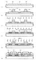
図6は本発明のイオンドーピング装置を用いたTFTの製造プロセスを示す一例を示す。まず、図6(A)において、アルミノホウケイ酸ガラスまたはバリウムホウケイ酸ガラスなどによる透光性の基板700上に多結晶シリコンで成る半導体膜702、703を形成する。また、基板700と半導体膜との間には、窒化シリコン、酸化シリコン、窒化酸化シリコンから選ばれた一つまたは複数種を組み合わせた第1絶縁膜701を50〜200nmの厚さで形成する。
【0047】
TFTのしきい値電圧を制御するためのチャネルドープは、この半導体膜に対して行い、1×10¹⁵〜1×10¹⁶/cm3の濃度でボロンをイオンドーピングにより添加する。勿論、ドーピングには図1及び図2で説明される本発明のイオンドーピング装置を用いる。
【0048】
その後、図6(B)に示すように、そして、第2絶縁膜704を80nmの厚さで形成する。第2絶縁膜704はゲート絶縁膜として利用するものであり、プラズマCVD法またはスパッタ法を用いて形成する。第2絶縁膜704として、SiH4とN2OにO2を添加させて作製する酸化窒化シリコン膜は膜中の固定電荷密度を低減させることが可能となり、ゲート絶縁膜として好ましい材料である。勿論、ゲート絶縁膜はこのような酸化窒化シリコン膜に限定されるものでなく、酸化シリコン膜や酸化タンタル膜などの絶縁膜を単層または積層構造として用いても良い。
【0049】
第2絶縁膜704上にゲート電極を形成するための第1導電膜を形成する。第1導電膜の種類に限定はないがAl、Ta、Ti、W、Moなどの導電性材料またはこれらの合金を適用することができる。このような材料を用いたゲート電極の構造は、窒化タンタル又は窒化チタンとW又はMo−W合金の積層構造、WとAl又はCuの積層構造などを採用することができる。Alを用いる場合には、耐熱性を高めるためにTi、Sc、Nd、Si、Cuなどを0.1〜7重量%添加したものを用いる。第1の導電膜は300nmの厚さで形成する。
【0050】
その後、レジストによる、マスク715を3μmの厚さに形成し、ドライエッチングにより第1の導電膜をエッチングしてゲート電極705、706を形成する。また、図示しないが、ゲート電極に接続する配線も同時に形成する。
【0051】
図6(C)に示すように、マスク715をそのまま残し、このゲート電極をマスクとして、図1及び図2で説明される本発明のイオンドーピング装置を用い、所定の不純物元素をイオンドーピングする。ドーピング処理の詳細は上述と同様にして行う。特に、この工程で行うイオンドーピングはマスク715、ゲート電極705、706を半導体膜702、703に対するマスクとして利用し、ゲート電極の外側の領域に1×10¹⁹〜1×10²¹/cm3の濃度となるようにリンイオンをイオンドーピングしてn型半導体領域707、708を形成する。また、図示しないが低濃度ドレイン(LDD)領域を形成する場合には、1×1017〜1×1019/cm3の濃度となるようにリンイオンをイオンドーピングにより添加する。
【0052】
リンイオンの注入が終了したら、マスク715をアッシングにより剥離する。続いて、図6(D)に示すように一方の半導体膜703にレジストによるマスク709を形成し、半導体膜702にボロンイオンをドーピングする。ドーズ量は1×10¹⁹〜5×10²¹/cm3とするが、n型を反転するためにリンよりも1.5〜3倍の濃度で添加されるようにする。
【0053】
ボロンイオンをドーピングした後、アッシングによりマスク709を除去する。その後、図6(E)に示すように酸化窒化シリコン膜または窒化シリコン膜から成る第3絶縁膜711をプラズマCVD法で50nmの厚さに形成する。
【0054】
そして、n型及びp型の半導体領域の結晶性の回復と、活性化のために熱処理を行う。熱処理はファーネスアニール炉の他、瞬間熱アニール、レーザーアニールなどの方法により行うことができる。
【0055】
図6(F)に示す第4絶縁膜712は、酸化シリコン膜、酸化窒化シリコンで形成する。または、ポリイミドまたはアクリルなどの有機絶縁物材料で形成し表面を平坦化しても良い。
【0056】
次いで、第4絶縁膜712の表面から各半導体膜の不純物領域に達するコンタクトホールを形成し、Al、Ti、Taなどを用いて配線を形成する。図6(F)において713、714はソース線またはドレイン電極となる。こうしてnチャネル型TFTとpチャネル型TFTを形成することができる。ここではそれぞれのTFTを単体として示しているが、これらのTFTを使ってCMOS回路やNMOS回路、PMOS回路を形成することができる。ここでは、TFTの製造プロセスを一例として示したが、プレーナプロセスによる半導体集積回路の製造プロセスにも適用することができる。
【0057】
【発明の効果】
本発明の構成を採用することにより、イオン源の温度を安定制御することが可能となり、これによってプラズマのイオン種割合が安定し、安定したドーピングを行うことができる。このイオンドーピング装置を用いてTFTを作製することで、安定したトランジスタ特性が得られる。
【0058】
また、図6を用いて説明したように、TFTを製造するための成膜、エッチング、ドーピングの各工程は枚葉処理により行われる。即ち、カセット毎に纏められた多数の基板を1枚毎に処理を行う。この場合、特にドーピング工程においては基板毎に注入されるイオン種の割合が変動すると、しきい値電圧やオフ電流値がばらつく要因となる。本発明によれば、このようなドーピング工程に係るばらつき要因を低減することができる。
【図面の簡単な説明】
【図1】 本発明のドーピング装置の一構成例を説明する図。
【図2】 本発明のドーピング装置のイオン源の構成の一形態を説明する図。
【図3】 水素で5%に希釈したジボランガスを用いた時に生成されるイオン種をE×B分離器により計測されたスペクトルを示すグラフ。
【図4】 二次イオン質量分析法(SIMS)で測定した質量数5のボロン元素の酸化シリコン膜中における深さ方向分布を示すグラフ。
【図5】 同一条件でチャネルドープを行って作製したTFTのしきい値電圧の基板間ばらつきを示すグラフ。
【図6】 TFTの製造工程を説明する図。[0001]
BACKGROUND OF THE INVENTION
The present invention relates to an ion doping apparatus and a doping method using the same, and more particularly to a highly accurate and highly reproducible ion doping technique used for forming impurity regions such as a source region and a drain region of a thin film transistor (TFT).
[0002]
[Prior art]
A technique of ionizing an impurity element for controlling valence electrons of a semiconductor and accelerating it by an electric field is known as an ion implantation method. In recent years, doping is performed by irradiating ions in a shower-like manner for the purpose of injecting an impurity element into a large-area substrate such as a liquid crystal display device.
[0003]
The ion doping apparatus has a configuration in which a doping chamber connected to an ion source is provided, the doping chamber is maintained in a vacuum, and a substrate is placed in the doping chamber to irradiate the surface of the substrate with an ion flow from the ion source. The ion source includes a plasma chamber, an extraction acceleration electrode system that extracts ions generated in the plasma chamber, and a deceleration electrode system that controls the inflow of secondary electrons. A porous electrode is generally used as the electrode, and ions pass through this hole to form an ion flow to the doping chamber.
[0004]
As a plasma generation method of the ion source, there are a direct current discharge method, a high frequency discharge method, a microwave discharge method, and the like. In addition, it is possible to confine the plasma inside the ion source by applying a magnetic field, and there is a case where a cusp magnetic field is formed by arranging a permanent magnet around the plasma chamber.
[0005]
[Problems to be solved by the invention]
In such an ion doping apparatus, mass separation is not performed in many cases, so that all the ion species (positive charges) formed in the plasma chamber are accelerated by the electric field generated by the extraction electrode and injected into the substrate. Become. The material gas used to obtain ions is diborane diluted with hydrogen (B) for gas stability.2H6) And phosphine (PHThree) Is often used. As a result, a large amount of hydrogen ions are simultaneously implanted in addition to the desired boron ions and phosphorus ions.
[0006]
For example, when phosphine is used as the material gas, H+, H2 +, HThree +, P+, PH+, PH2 +, PHThree +And so on. The abundance ratio of these ion species varies depending on the dilution ratio of the material gas and the plasma generation conditions. If the electric field is accelerated without mass separation, these ions are irradiated onto the substrate.
[0007]
FIG. 3 shows the spectrum of the ion species generated when diborane gas diluted to 5% with hydrogen is measured by an E × B separator. B near mass number 202H y +In addition to observing ion peaks, H of
[0008]
In the ion doping apparatus, the Faraday cup ammeter is used to monitor the ion current, thereby controlling the dose while monitoring the dose. However, what is measured by the Faraday cup ammeter is a total ion current obtained by adding ions of a diluent gas in addition to impurity ions for valence electron control. Accordingly, when the ratio of ion species generated in the plasma chamber changes, the amount of impurity ions to be implanted changes.
[0009]
FIG. 4 is a graph showing the distribution in the depth direction in the silicon oxide film of elements (boron) having a mass number of 10 and 11 measured by secondary ion mass spectrometry (SIMS). It shows the concentration change when the substrate is sequentially doped. Although this data is performed at the same dose amount setting, the boron concentration increases as the number of dopings increases, that is, the latter half of the doping process. This result shows that the proportion of ionic species containing boron increases as the number of doping increases.
[0010]
Further, FIG. 5 shows the variation in the net threshold voltage between the substrates of the TFT manufactured by channel doping under the same conditions. Even in this case, it is observed that the threshold voltage tends to shift to the positive side as the number of doping increases (as the number of doped substrates increases). This result means that the amount of boron injected is increasing. In this way, the product cannot be produced with good reproducibility due to the concentration of the impurity element for controlling the valence electrons to be injected, even though the treatment is performed under the same doping conditions.
[0011]
The present invention has been made in view of such problems, and provides an ion doping apparatus capable of stabilizing the ratio of ion species to be implanted and controlling the doping amount with high accuracy in the ion doping apparatus. For the purpose.
[0012]
[Means for Solving the Problems]
In order to solve the above problems, an ion doping apparatus according to the present invention includes a gas introduction unit, an ion generation unit, and a drawing acceleration unit, and an ion source surrounded by a wall having a gap with a double structure, an ion A doping chamber having holding means connected to the source and holding the substrate exposed to the ion flow of the ions is provided, and the gap portion is filled with a heating or cooling medium.
[0013]
In addition, an ion source including a gas introduction unit, an ion generation unit including a predetermined impurity element, and an extraction acceleration unit, a heating or cooling unit that maintains the temperature of the inner wall of the ion source at a constant temperature, and an ion source A doping chamber having holding means for holding the substrate connected to and exposed to the ion flow of the ions is provided. The temperature of the inner wall of the ion source is preferably maintained at a constant temperature of 100 ° C. or higher, or a constant temperature of 0 ° C. or lower. In any case, the temperature of the inner wall of the ion source rises by self-heating by the ion generating means. It is important to maintain a constant temperature by heating or cooling to a temperature below room temperature.
[0014]
As means for keeping the temperature of the inner wall of the ion source constant, the temperature control means includes a temperature sensor that senses the surface temperature of the inner wall of the ion source and a feedback circuit that controls the target temperature based on the detection result of the temperature sensor. The temperature can be controlled with higher accuracy.
[0015]
In the above configuration of the present invention, the temperature of the inner wall of the ion source is constant.InBy holding, the abundance ratio of ionic species becomes constant, that is, the ion species to be implanted and the abundance ratio thereof can be stabilized. Thereby, an ion doping apparatus capable of controlling the dose amount with high accuracy can be provided.
[0016]
According to the ion doping method of the present invention, the temperature of the inner wall of an ion source provided with means for generating ions containing a predetermined impurity element and extraction acceleration means is maintained at a constant temperature, and the abundance ratio of a plurality of ion species is maintained constant. In this state, the object to be processed is doped with ions accelerated by an electric field. In particular, it is preferable that the temperature of the inner wall of the ion source is maintained at a constant temperature of 100 ° C. or higher or a constant temperature of 0 ° C. or lower.
[0017]
In the above configuration of the present invention, the temperature of the inner wall of the ion source is constant.InBy holding, the existence ratio of the ion species becomes constant, and the fluctuation of the dose amount can be prevented in the ion doping process, that is, the ion species to be implanted and the existence ratio thereof can be stabilized. Thereby, ion doping capable of controlling the dose amount with high accuracy can be performed.
[0018]
The following considerations have been made regarding the cause of fluctuations in ion species. Table 1 shows control parameters in the ion doping apparatus.
[0019]
[Table 1]
These control parameters show actual values in the channel doping process performed in FIG. From Table 1, the FC beam current, implantation total dose, and implantation time are stable during ion doping, and the parameters of the filament, arc, acceleration system, and vacuum system are also stable. Based on the above facts, it is considered that the temperature of the ion source, more specifically the temperature of the inner wall of the ion source, influences the ion species ratio as a cause of the fluctuation of the ion species existence ratio. That is, it is considered that as the number of doping treatments increases, the temperature of the inner wall of the ion source, the filament temperature rises, and the plasma electron temperature fluctuates, and as a result, the proportion of ion species in the plasma increases. Therefore, if the temperature of the ion source can be controlled to be constant, the ion species ratio can be stabilized, and ion doping can be stabilized.
[0021]
DETAILED DESCRIPTION OF THE INVENTION
Hereinafter, embodiments of the present invention will be described in detail with reference to the accompanying drawings.
[0022]
The main configuration of the present invention includes a gas introduction unit, an ion source including an ion generation unit including a predetermined impurity element, and an extraction acceleration unit, and a substrate that is connected to the ion source and is exposed to an ion flow of the ion. In a configuration including a doping chamber having a holding means for holding, a temperature control means is provided around the ion source. By this temperature control means, the temperature is controlled to be higher or lower than the self-heating temperature of the ion source and maintained at a constant temperature to keep the abundance ratio of ionic species constant.
[0023]
The ion source rises in temperature by applying direct current or high frequency power to generate plasma. On the other hand, by keeping the temperature of the ion source from the beginning, specifically, the temperature of the inner wall of the ion source higher than that, preferably 100 ° C. or higher, the temperature of the inner wall can be controlled to be constant. . Or it is the same even if it cools below room temperature, Preferably it is 0 degrees C or less.
[0024]
As the temperature control means, a heating wire is used for the purpose of heating. Specifically, a Ni—Cr alloy (nichrome wire) is used. Thereby, the maximum use temperature can be heated to about 1000 ° C. In the case of a Ni—Cr—Al based alloy (kanthal wire), it can be used up to 1200 ° C. These heating elements are wound around the periphery of the outer wall of the ion source. It is also possible to use a sheath wire heater in which these heating elements are insulated and incorporated in a stainless steel or Inconel thin tube with a powder of a heat-resistant insulating material such as magnesium oxide. Platinum or a platinum-rhodium alloy can also be used as a heating element. An induction furnace can also be used to install a heating element inside the ion source. Alternatively, the ion source may be formed of a double-structured wall having a gap, and the gap may be filled with a heating or cooling medium. As the medium, silicon oil, liquid nitrogen, liquid helium, or the like can be used.
[0025]
In the case of cooling the ion source, if the temperature of the inner wall of the ion source rises too much with respect to the set temperature, the ion species ratio increases. At this time, the ion source ratio is actively cooled to suppress the increase in the ion species ratio. Conversely, when the temperature is too low, the ion source is actively heated. In this way, the abundance ratio of ionic species is stabilized. To cool the ion source, a large number of cooling tubes are arranged around the ion source. A refrigerant is circulated in the cooling pipe. As the refrigerant, silicon oil, liquid nitrogen, liquid oxygen, liquid helium, or the like is used. Further, at a position away from the ion source, the temperature of the refrigerant is lowered using a heat exchanger, a compressor, an electronic cooler using a Peltier element, or the like. In addition, low temperature gas may be sprayed directly on the outer periphery of the ion source. For example, dry nitrogen is used as the low temperature gas. Further, an uneven heat sink may be provided so as to make the surface area of the ion source outer peripheral portion as large as possible so that the ion source outer peripheral portion and the ambient air effectively exchange heat.
[0026]
High precisionInIn order to control the temperature of the ion source, a temperature sensor that senses the surface temperature of the inner wall of the ion source, and a feedback circuit that controls the target temperature based on the detection result of the temperature sensorTheProvided in the temperature control means. A thermocouple is used as a typical temperature sensor. Thermocouple K (Chromel-Alumel) can be used up to 1200 ° C. in an oxidizing atmosphere. A platinum-rhodium system (thermocouples B, R, S, etc.) can be used from 1600 ° C. to 1700 ° C., is stable in an oxidizing atmosphere, has heat resistance, and can be measured with high accuracy. Further, by using a tungsten, molybdenum, rhenium, or tantalum-based thermocouple, higher temperature measurement is possible. In addition, a metal resistance thermometer or a thermistor resistance thermometer may be used as the resistance thermometer. The metal resistance thermometer has a temperature measurement range of about −200 to 600 ° C., but a measurement accuracy one digit higher than that of the thermocouple can be obtained. Alternatively, the temperature of the plasma may be measured by providing a quartz window on the side wall of the ion source and installing a radiation thermometer outside the ion source.
[0027]
FIG. 1 is a diagram showing an embodiment of an ion doping apparatus of the present invention. A doping apparatus according to the present invention includes an
[0028]
The
[0029]
The details of the
[0030]
Similarly to a normal ion source, a
[0031]
As the extraction electrode system, an
[0032]
The doping gas is PHThree, B2H6The one diluted with hydrogen or inert gas to about 0.1 to 20% is used. PHThreeIn the case of PHx +, P2Hx +, Hx +Are generated as ion species, and when mass separation is not performed, these ions are accelerated by the extraction electrode system and extracted to the doping chamber in which the substrate is installed. Ions are extracted almost linearly by the four electrodes and irradiated onto the substrate.
[0033]
The
[0034]
By forming the inner surface of the
[0035]
With the configuration as described above, fluctuations in the abundance ratio of various ions generated in the ion source can be suppressed, ion doping processing with high reproducibility can be performed, and the concentration of the impurity element can be controlled with high accuracy.
[0036]
FIG. 2 shows another ion source configuration applicable to the ion doping apparatus of the present invention. The
[0037]
The
[0038]
As extraction acceleration means, an
[0039]
A doping method using such an ion doping apparatus will be described based on the apparatus having the configuration shown in FIG.
[0040]
First, the
[0041]
The substrate to be doped is carried in from the
[0042]
When the substrate is carried into the
[0043]
When the processing is completed, the application of power to the filament and the supply of the material gas are stopped, and the ion irradiation is stopped. The doped substrate is collected in the unload
[0044]
The
[0045]
By such a process, fluctuations in the abundance ratio of various ions generated in the ion source can be suppressed, ion reproducibility with high reproducibility can be performed, and the concentration of the impurity element can be controlled with high accuracy.
[0046]
FIG. 6 shows an example of a manufacturing process of a TFT using the ion doping apparatus of the present invention. First, in FIG. 6A,
[0047]
Channel doping for controlling the threshold voltage of the TFT is performed on this semiconductor film.15~ 1x10¹⁶/cmThreeBoron is added by ion doping at a concentration of Of course, the ion doping apparatus of the present invention described with reference to FIGS. 1 and 2 is used for doping.
[0048]
Thereafter, as shown in FIG. 6B, a second
[0049]
A first conductive film for forming a gate electrode is formed over the second
[0050]
Thereafter, a resist
[0051]
As shown in FIG. 6C, the
[0052]
When the phosphorus ion implantation is completed, the
[0053]
After doping with boron ions, the
[0054]
Then, heat treatment is performed to recover and activate the crystallinity of the n-type and p-type semiconductor regions. In addition to the furnace annealing furnace, the heat treatment can be performed by methods such as rapid thermal annealing and laser annealing.
[0055]
The fourth
[0056]
Next, a contact hole reaching the impurity region of each semiconductor film from the surface of the fourth insulating
[0057]
【The invention's effect】
By adopting the configuration of the present invention, it becomes possible to stably control the temperature of the ion source, whereby the ion species ratio of plasma is stabilized, and stable doping can be performed. Stable transistor characteristics can be obtained by manufacturing TFTs using this ion doping apparatus.
[0058]
Further, as described with reference to FIG. 6, film formation, etching, and doping processes for manufacturing a TFT are performed by single wafer processing. That is, a large number of substrates collected for each cassette are processed one by one. In this case, particularly in the doping step, if the ratio of ion species implanted for each substrate varies, the threshold voltage and the off-current value may vary. According to the present invention, it is possible to reduce such a variation factor related to the doping process.
[Brief description of the drawings]
FIG. 1 is a diagram illustrating a configuration example of a doping apparatus of the present invention.
FIG. 2 is a diagram illustrating one embodiment of a configuration of an ion source of a doping apparatus of the present invention.
FIG. 3 is a graph showing a spectrum obtained by measuring an ion species generated by using an E × B separator when diborane gas diluted to 5% with hydrogen is used.
FIG. 4 is a graph showing the distribution in the depth direction in a silicon oxide film of a boron element having a mass number of 5 measured by secondary ion mass spectrometry (SIMS).
FIG. 5 is a graph showing the variation between the substrates in the threshold voltage of a TFT manufactured by channel doping under the same conditions.
6A and 6B are diagrams illustrating a manufacturing process of a TFT.
Claims (11)
Priority Applications (1)
| Application Number | Priority Date | Filing Date | Title |
|---|---|---|---|
| JP2002104586A JP4037149B2 (en) | 2002-04-05 | 2002-04-05 | Ion doping apparatus and ion doping method |
Applications Claiming Priority (1)
| Application Number | Priority Date | Filing Date | Title |
|---|---|---|---|
| JP2002104586A JP4037149B2 (en) | 2002-04-05 | 2002-04-05 | Ion doping apparatus and ion doping method |
Publications (3)
| Publication Number | Publication Date |
|---|---|
| JP2003303784A JP2003303784A (en) | 2003-10-24 |
| JP2003303784A5 JP2003303784A5 (en) | 2005-09-08 |
| JP4037149B2 true JP4037149B2 (en) | 2008-01-23 |
Family
ID=29389735
Family Applications (1)
| Application Number | Title | Priority Date | Filing Date |
|---|---|---|---|
| JP2002104586A Expired - Fee Related JP4037149B2 (en) | 2002-04-05 | 2002-04-05 | Ion doping apparatus and ion doping method |
Country Status (1)
| Country | Link |
|---|---|
| JP (1) | JP4037149B2 (en) |
Families Citing this family (4)
| Publication number | Priority date | Publication date | Assignee | Title |
|---|---|---|---|---|
| JP2007266022A (en) * | 2004-05-25 | 2007-10-11 | Matsushita Electric Ind Co Ltd | Plasma generator, plasma treating apparatus using same, and electronic apparatus |
| JP5030484B2 (en) * | 2005-06-30 | 2012-09-19 | 株式会社半導体エネルギー研究所 | Method for manufacturing semiconductor device |
| JP2017037861A (en) * | 2013-12-18 | 2017-02-16 | 株式会社アルバック | Plasma doping device and method |
| CN109148247B (en) * | 2017-06-16 | 2024-01-16 | 上海凯世通半导体股份有限公司 | Ion implantation apparatus and method |
-
2002
- 2002-04-05 JP JP2002104586A patent/JP4037149B2/en not_active Expired - Fee Related
Also Published As
| Publication number | Publication date |
|---|---|
| JP2003303784A (en) | 2003-10-24 |
Similar Documents
| Publication | Publication Date | Title |
|---|---|---|
| JP3647506B2 (en) | Method for forming an insulator layer on a semiconductor substrate | |
| US6138606A (en) | Ion implanters for implanting shallow regions with ion dopant compounds containing elements of high solid solubility | |
| US7023138B2 (en) | Electron impact ion source | |
| US5061642A (en) | Method of manufacturing semiconductor on insulator | |
| US8129202B2 (en) | Plasma doping method and apparatus | |
| US9136282B2 (en) | Memories and methods of forming thin-film transistors using hydrogen plasma doping | |
| US7790586B2 (en) | Plasma doping method | |
| US7754503B2 (en) | Method for producing semiconductor device and semiconductor producing apparatus | |
| TWI277168B (en) | Methods for forming thin film layers by simultaneous doping and sintering | |
| JP4037149B2 (en) | Ion doping apparatus and ion doping method | |
| JPH03269940A (en) | Manufacture of ion implantation device and semiconductor integrated circuit device thereof | |
| WO2004109784A1 (en) | Ion doping system, ion doping method and semiconductor device | |
| US20050037559A1 (en) | Method of manufacturing a semiconductor device | |
| TW414977B (en) | Method of rapid thermal processing (RTP) of ion implanted silicon | |
| Bertoldo et al. | New method for the production of thin and stable, segmented n+ contacts in HPGe detectors | |
| JPH0758695B2 (en) | Plasma doping method | |
| TWI281692B (en) | Ion implantation apparatus and method | |
| JP4860287B2 (en) | Doping method and manufacturing method of field effect transistor | |
| US20230369009A1 (en) | Ion implantation system | |
| US20150118833A1 (en) | Method of making source/drain contacts by sputtering a doped target | |
| Lee | Ti+ and Mg+ Ion beam extraction from the modified bernas ion source | |
| EP0544470A1 (en) | Thin film transistor, method of fabricating the same and ion implantation method used in the fabrication | |
| JP3578345B2 (en) | Semiconductor device manufacturing method and semiconductor device | |
| JP3202002B2 (en) | Impurity introduction device and impurity introduction method | |
| Cheng et al. | Diffusion and Ion Implantation Equipment |
Legal Events
| Date | Code | Title | Description |
|---|---|---|---|
| A521 | Written amendment |
Free format text: JAPANESE INTERMEDIATE CODE: A523 Effective date: 20050318 |
|
| A621 | Written request for application examination |
Free format text: JAPANESE INTERMEDIATE CODE: A621 Effective date: 20050318 |
|
| A977 | Report on retrieval |
Free format text: JAPANESE INTERMEDIATE CODE: A971007 Effective date: 20070727 |
|
| A131 | Notification of reasons for refusal |
Free format text: JAPANESE INTERMEDIATE CODE: A131 Effective date: 20070807 |
|
| A521 | Written amendment |
Free format text: JAPANESE INTERMEDIATE CODE: A523 Effective date: 20070927 |
|
| TRDD | Decision of grant or rejection written | ||
| A01 | Written decision to grant a patent or to grant a registration (utility model) |
Free format text: JAPANESE INTERMEDIATE CODE: A01 Effective date: 20071030 |
|
| A61 | First payment of annual fees (during grant procedure) |
Free format text: JAPANESE INTERMEDIATE CODE: A61 Effective date: 20071031 |
|
| R150 | Certificate of patent or registration of utility model |
Free format text: JAPANESE INTERMEDIATE CODE: R150 |
|
| FPAY | Renewal fee payment (event date is renewal date of database) |
Free format text: PAYMENT UNTIL: 20101109 Year of fee payment: 3 |
|
| FPAY | Renewal fee payment (event date is renewal date of database) |
Free format text: PAYMENT UNTIL: 20101109 Year of fee payment: 3 |
|
| FPAY | Renewal fee payment (event date is renewal date of database) |
Free format text: PAYMENT UNTIL: 20101109 Year of fee payment: 3 |
|
| FPAY | Renewal fee payment (event date is renewal date of database) |
Free format text: PAYMENT UNTIL: 20111109 Year of fee payment: 4 |
|
| FPAY | Renewal fee payment (event date is renewal date of database) |
Free format text: PAYMENT UNTIL: 20111109 Year of fee payment: 4 |
|
| FPAY | Renewal fee payment (event date is renewal date of database) |
Free format text: PAYMENT UNTIL: 20121109 Year of fee payment: 5 |
|
| FPAY | Renewal fee payment (event date is renewal date of database) |
Free format text: PAYMENT UNTIL: 20121109 Year of fee payment: 5 |
|
| FPAY | Renewal fee payment (event date is renewal date of database) |
Free format text: PAYMENT UNTIL: 20131109 Year of fee payment: 6 |
|
| R250 | Receipt of annual fees |
Free format text: JAPANESE INTERMEDIATE CODE: R250 |
|
| R250 | Receipt of annual fees |
Free format text: JAPANESE INTERMEDIATE CODE: R250 |
|
| R250 | Receipt of annual fees |
Free format text: JAPANESE INTERMEDIATE CODE: R250 |
|
| R250 | Receipt of annual fees |
Free format text: JAPANESE INTERMEDIATE CODE: R250 |
|
| LAPS | Cancellation because of no payment of annual fees |