JP4036048B2 - Defect identification method - Google Patents
Defect identification method Download PDFInfo
- Publication number
- JP4036048B2 JP4036048B2 JP2002206784A JP2002206784A JP4036048B2 JP 4036048 B2 JP4036048 B2 JP 4036048B2 JP 2002206784 A JP2002206784 A JP 2002206784A JP 2002206784 A JP2002206784 A JP 2002206784A JP 4036048 B2 JP4036048 B2 JP 4036048B2
- Authority
- JP
- Japan
- Prior art keywords
- defect
- value
- pixel
- contour
- inspection object
- Prior art date
- Legal status (The legal status is an assumption and is not a legal conclusion. Google has not performed a legal analysis and makes no representation as to the accuracy of the status listed.)
- Expired - Fee Related
Links
Images


Landscapes
- Investigating Materials By The Use Of Optical Means Adapted For Particular Applications (AREA)
- Testing Of Optical Devices Or Fibers (AREA)
- Testing Or Measuring Of Semiconductors Or The Like (AREA)
- Image Processing (AREA)
- Image Analysis (AREA)
Description
【0001】
【発明の属する技術分野】
本発明は、液晶、PDP等の透過性があるガラス基板を用いた製品における表面のパターン欠陥、異物などの検査において、裏面の欠陥が製品の良否に影響しないため表面の欠陥のみを検出すればよい場合などに、検出された欠陥がガラス基板の表面の欠陥か裏面の欠陥かを識別する方法に関するものである。
【0002】
【従来の技術】
従来の欠陥識別方法について、図8から図9を用いて説明する。
【0003】
図8は従来の欠陥検査装置の概略構成図である。
【0004】
図8において、1は検査対象物、2は検査対象物1に照明光を照射する照明光源、3は照明光源2により照明光を照射された検査対象物1を撮像する画像入力部、4は画像入力部3により入力された画像を処理するための画像処理部である。検査対象物1において、画像入力部3側を表面とし、1aは検査対象物1の表面、1bは検査対象物1の裏面である。
【0005】
従来の欠陥検査は照明光源2により照明光を検査対象物1に照射し、照明光を照射された検査対象物1を画像入力部3により撮像する。画像入力部3により撮像した画像データを画像処理部4により処理し、欠陥の検査を行っていた。
【0006】
しかし、画像入力部3は検査対象物1の表面1aに焦点が合うように調整されており、検査対象物1の裏面1bに存在する欠陥は焦点が合わずコントラストが落ち、欠陥領域中に明るい部分が占める割合が増える。そこで、検出された欠陥の各画素の明るさを表す階調値の平均値を計算し、計算された平均値が設定されたしきい値より大きい場合には該当欠陥を検査対象物1の裏面1bの欠陥とし、計算された平均値が設定されたしきい値以下の場合には当該欠陥を検査対象物1の表面1aの欠陥とすることにより、検査対象物1の表面1aの欠陥か裏面1bの欠陥かを識別するようにしていた。
【0007】
以下、図9を用いて具体的に説明する。
【0008】
画像入力部3により撮像した画像データは画像処理部4において、各画素毎に0〜255の256階調の正数値で明るさを表す。階調値が255に近づくほど画素の明るさは明るく、0に近づくほど画素の明るさは暗いものとする。
【0009】
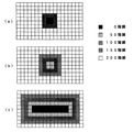
図9(a)に示すような検査対象物1の表面1aの欠陥は、欠陥領域の明るさを表す階調値の平均値が75となる。それに対し、図9(b)に示すような検査対象物1の裏面1bの小さな欠陥は、欠陥領域の明るさを表す階調値の平均値が88となる。検査対象物1の表面1aの欠陥であれば、画像入力部3の焦点が合わせられているため欠陥領域の輪郭がはっきりしており、実験やサンプリングにより欠陥領域の明るさを表す階調値の平均値は10〜80程度の範囲になっていた。そこで、表面1aの欠陥と裏面1bの欠陥を識別するためのしきい値を80とすることにより、図9(a)の表面1aの欠陥と図9(b)の裏面1bの欠陥は識別が可能であった。ここで、しきい値を80としたが、しきい値は検査対象物1の透過性や欠陥領域の光り方により変化するものであるため、この値に限るものではない。
【0010】
しかし、図9(c)に示すような検査対象物1の裏面1bの大きな欠陥であると、欠陥領域の中央部において各画素の階調値が小さく、欠陥領域の明るさを表す階調値の平均値が60となる。このような平均値になると、表面1aの欠陥領域の明るさを表す階調値の平均値と差がなくなり、図9(a)の表面1aの欠陥と図9(c)の裏面1bの欠陥をしきい値で識別することが困難であった。
【0011】
【発明が解決しようとする課題】
上記に示したように従来の方法では、裏面の欠陥の大きさが大きくなるにしたがって、欠陥領域の明るさを表す階調値の平均値が表面の欠陥領域の明るさを表す階調値の平均値に近づいていくため、欠陥領域の明るさを表す階調値の平均値を用いて、しきい値により表面の欠陥か裏面の欠陥かを識別することが困難であった。
【0012】
本発明は、欠陥領域の輪郭を抽出し、欠陥領域の輪郭のコントラストにより検査対象物の表面の欠陥と裏面の欠陥を高精度に識別することが可能となる。これにより、表面の欠陥のみを不良とする、裏面の欠陥のみを不良とする、表面の欠陥、裏面の欠陥それぞれの集計をするといった、実際の製造ラインに即した検査が可能となる。
【0013】
【課題を解決するための手段】
上記課題を解決するために本発明は、透過性がある検査対象物の欠陥を検出する欠陥検査方法において、第一のしきい値以下の暗い欠陥領域または第二のしきい値以上の明るい欠陥領域を検出し、前記欠陥領域について輪郭を抽出し、前記輪郭の画素の階調値と前記輪郭の画素に隣接する画素の階調値との差の最大値を算出し、前記欠陥領域の全輪郭の画素について前記最大値の平均値を算出し、前記平均値と第三のしきい値を比較することにより、前記検査対象物の表面の欠陥か裏面の欠陥かを識別することが可能となる。
【0014】
さらに、最大値の平均値を算出する工程において、欠陥領域の全輪郭の画素について前記最大値を小さい順に並べ、前記最大値について予め設定した個数または割合をもとに小さい方から選択し、前記選択した複数の最大値の平均値を算出することにより、検査対象物の表面の欠陥と裏面の欠陥をより高精度に識別することが可能となる。
【0015】
また、検査対象物上にパターンが存在する場合、欠陥領域を検出する工程の前に、予め登録されたパターンとの差画像データを作成することにより、検査対象物上にパターンが存在する場合にも検査対象物の表面の欠陥と裏面の欠陥を高精度に識別することが可能となる。
【0016】
【発明の実施の形態】
本発明の実施の形態について、図1から図7を用いて説明する。
【0017】
本発明の実施の形態における欠陥検査装置は、図8に示す従来の欠陥検査装置と同様の装置を用いる。
【0018】
本発明における第一の実施の形態について、図1から図3を用いて説明する。
【0019】
図1は第一の実施の形態におけるフローチャートである。
【0020】
まず、照明光源2により照明光を検査対象物1に照射し、照明光を照射された検査対象物1を画像入力部3により撮像する。画像入力部3により撮像した画像データを画像処理部4に入力する(S11)。
【0021】
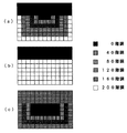
次に、S11にて入力した画像データに対して、階調値が第一のしきい値以下の領域を暗い欠陥領域として検出する(S12)。図2は図9の画像データに対して、第一のしきい値を100とし、第一のしきい値以下の領域を欠陥とするときの検出された欠陥領域を示す。図2(a)は図9(a)に対する欠陥領域、図2(b)は図9(c)に対する欠陥領域である。ここで、第一のしきい値を100としたが、第一のしきい値は検査対象物1の透過性や欠陥領域の光り方により変化するものであるため、この値に限るものではない。
【0022】
次に、S12にて検出された暗い欠陥領域の画素について、階調値が第一のしきい値より大きい画素が周囲に存在する画素を欠陥領域の輪郭として抽出する(S13)。図3は図2の欠陥領域に対して、第一のしきい値より大きい画素が周囲に存在する画素を輪郭としたときの欠陥領域の輪郭である。図3(a)は図2(a)に対する輪郭、図3(b)は図2(b)に対する輪郭である。
【0023】
次に、S13にて検出された輪郭について、輪郭の画素の階調値と輪郭の画素の周囲に隣接して存在する画素の階調値との差の最大値を算出する(S14)。例えば、図3(a)における輪郭の画素D1について算出すると、輪郭の画素D1の階調値は100であり、輪郭の画素D1の上側に隣接する画素の階調値は100、輪郭の画素D1の右側に隣接する画素の階調値は200、輪郭の画素D1の下側に隣接する画素の階調値は100、輪郭の画素D1の左側に隣接する画素の階調値は0であるので、輪郭の画素D1の階調値と輪郭の画素D1に隣接する画素の階調値との差の最大値は100となる。また、図3(b)における輪郭の画素D2について算出すると、輪郭の画素D2の階調値は100であり、輪郭の画素D2の上側に隣接する画素の階調値は100、輪郭の画素D2の右側に隣接する画素の階調値は150、輪郭の画素D2の下側に隣接する画素の階調値は100、輪郭の画素D2の左側に隣接する画素の階調値は50であるので、輪郭の画素D2の階調値と輪郭の画素D2に隣接する画素の階調値との差の最大値は50となる。
【0024】
次に、S14にて全輪郭の画素について算出した輪郭の画素の階調値と輪郭の画素に隣接する画素の階調値との差の最大値について、全輪郭の画素における最大値の平均を算出する(S15)。例えば、図3(a)の全輪郭の画素における最大値の平均は100となる。また、図3(b)の全輪郭の画素における最大値の平均は50となる。
【0025】
次に、S15にて算出した平均値が大きいほど、コントラストがはっきりしていることになるため、平均値が第三のしきい値以上であれば検査対象物1の表面1aの欠陥、第三のしきい値より小さければ検査対象物1の裏面1bの欠陥として識別する(S16)。例えば、欠陥識別を行うための第三のしきい値を80とすると、図3(a)では欠陥領域の輪郭における平均値は100であり、第三のしきい値80以上であるので検査対象物1の表面1aの欠陥と識別される。また、図3(b)では欠陥領域の輪郭における平均値は50であり、第三のしきい値80より小さいので検査対象物1の裏面1bの欠陥と識別される。ここで、第三のしきい値を80としたが、第三のしきい値は検査対象物1の透過性により変化するものであるため、この値に限るものではなく、実験やサンプリングにより決定することが望ましい。
【0026】
以上のように本発明の第一の実施の形態によれば、従来の欠陥識別方法では裏面1bの欠陥として識別が困難であった、図9(c)のような裏面1bに存在する大きな欠陥を、裏面1bの欠陥として識別することが可能となり、検査対象物1の表面1aの欠陥と裏面1bの欠陥を高精度に識別することが可能となる。
【0027】
次に、本発明における第二の実施の形態について、図4から図7を用いて説明する。
【0028】
図4は第二の実施の形態におけるフローチャートである。
【0029】
本発明における第二の実施の形態では、検査対象物1上にパターンが存在する場合に、予め登録しておいた良品パターンまたは繰返し性のあるパターンとの差画像を作成し欠陥の検出を行う。
【0030】
まず、画像入力部3により撮像した検査対象物1の画像データを画像処理部4に入力する(S21)。
【0031】
次に、S21にて入力された画像データと予め登録しておいたパターンの画像データより差画像データを作成する(S22)。図5(a)はS21で入力した画像データ、図5(b)は予め登録しておいたパターンの画像データであり、図5(a)と図5(b)を差画像比較し、図5(c)の差画像データを作成する。差画像データを作成する際に、画素の明るさを表す階調値を0〜255の256階調の正数値にしているため、非欠陥領域の階調値を256階調の中心値である128とし画素の明暗を明確にしている。ここでは説明をわかりやすくする目的で非欠陥領域の階調値を120としている。また、マイナス値になる画素の階調値は0としている。
【0032】
次に、S22にて作成した差画像データに対して、欠陥領域を検出する(S23)。図6は図5(c)の差画像データに対して、第一のしきい値を100とし、第一のしきい値以下の領域を欠陥とするときの検出された欠陥領域を示す。ここで、第一のしきい値を100としたが、第一のしきい値は検査対象物1の透過性や欠陥領域の光り方により変化するものであるため、この値に限るものではない。
【0033】
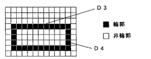
次に、S23にて検出された欠陥領域の輪郭を抽出する(S24)。図7は図6の欠陥領域に対して、第一のしきい値より大きい画素が周囲に存在する画素を輪郭としたときの欠陥領域の輪郭である。
【0034】
次に、S24にて検出された輪郭について、輪郭の画素の階調値と輪郭の画素の周囲に隣接して存在する画素の階調値との差の最大値を算出する(S25)。例えば、図7における輪郭の画素D3について算出すると、輪郭の画素D3の階調値は0であり、輪郭の画素D3の上側に隣接する画素の階調値は120、輪郭の画素D3の右側に隣接する画素の階調値は0、輪郭の画素D3の下側に隣接する画素の階調値は0、輪郭の画素D3の左側に隣接する画素の階調値は0であるので、輪郭の画素D3の階調値と輪郭の画素D3に隣接する画素の階調値との差の最大値は120となる。また、輪郭の画素D4について算出すると、輪郭の画素D4の階調値は80であり、輪郭の画素D4の上側に隣接する画素の階調値は80、輪郭の画素D4の右側に隣接する画素の階調値は120、輪郭の画素D4の下側に隣接する画素の階調値は80、輪郭の画素D4の左側に隣接する画素の階調値は40であるので、輪郭の画素D4の階調値と輪郭の画素D4に隣接する画素の階調値との差の最大値は40となる。
【0035】
次に、S25にて全輪郭の画素について算出した輪郭の画素の階調値と輪郭の画素に隣接する画素の階調値との差の最大値について、予め設定した個数または割合をもとに最大値を小さい方から選択し、選択した複数の最大値の平均を算出する(S26)。例えば、図7においては、全輪郭の画素の個数が28個であり、最大値が40の画素が19個、最大値が80の画素が2個、最大値が120の画素が7個である。予め設定した割合を50%とすると、平均を算出するための最大値の個数は14個であり、最大値が小さい方から14個分の平均は40となる。ここで、予め設定した割合を50%としたが、予め設定する割合は、欠陥と予め登録されているパターンとが重なりあっている場合に、欠陥と予め登録されているパターンとが重なっている部分の影響を軽減するためであり、割合が大きすぎると欠陥の輪郭がパターンの輪郭と重なっている部分が多く含まれ誤判定したり、割合が小さすぎると輪郭がノイズの影響によりコントラストが悪くなっている部分で判定してしまい誤判定してしまったりする。したがって、予め設定する割合は30〜50%の範囲内が好適である。しかし、予め設定する割合は、欠陥の大きさや予め登録されているパターンにより変化するものであるため、この値に限るものではない。
【0036】
次に、S26にて算出した平均値に対して、平均値が第三のしきい値以上であれば検査対象物1の表面1aの欠陥、第三のしきい値より小さければ検査対象物1の裏面1bの欠陥として識別する(S27)。例えば、欠陥識別を行うための第三のしきい値を80とすると、図7では欠陥領域の輪郭における平均値は40であり、第三のしきい値80より小さいので検査対象物1の裏面1bの欠陥と識別される。ここで、第三のしきい値を80としたが、第三のしきい値は検査対象物1の透過性により変化するものであるため、この値に限るものではなく、実験やサンプリングにより決定することが望ましい。
【0037】
以上のように本発明の第二の実施の形態によれば、本発明の第一の実施の形態では裏面1bの欠陥として識別が困難であった、欠陥とパターンが重なった部分が大きい裏面1bに存在する欠陥を、裏面1bの欠陥として識別することが可能となり、検査対象物1上にパターンが存在する場合にも検査対象物1の表面1aの欠陥と裏面1bの欠陥を高精度に識別することが可能となる。
【0038】
また、本発明の実施の形態においては、照明光を検査対象物1の裏面1b側から照射する装置構成を用いたが、検査対象物1の表面1a側から照明光を照射する構成を用いてもよく、検査対象物1の表面1a側から照明光を照射する構成を用いた場合には、検査対象物1の裏面1bの欠陥が光るようになるため、画像処理上は、明暗部が反転するだけであり、欠陥領域検出において、階調値が第二のしきい値以上の領域を明るい欠陥領域として検出するようにすればよい。
【0039】
また、本発明の実施の形態においては、輪郭の画素に隣接する画素を、輪郭の画素に隣接する8つの画素の内、上下左右に隣接する4つの画素としたが、前記4つの画素を除く4つの画素としてもよく、8つの画素全てにしてもよい。
【0040】
また、輪郭の画素の階調値と輪郭の画素に隣接する画素の階調値との差は、2乗値や絶対値などを用いてもよい。
【0041】
【発明の効果】
以上のように本発明によれば、透過性がある検査対象物の表面の欠陥と裏面の欠陥を高精度に識別することが可能となる。
【0042】
さらに、検査対象物上にパターンが存在する場合にも、差画像データを作成することにより検査対象物の表面の欠陥と裏面の欠陥を高精度に識別することが可能となる。
【0043】
これにより、表面の欠陥のみを不良とする、裏面の欠陥のみを不良とする、表面の欠陥、裏面の欠陥それぞれの集計をするといった、実際の製造ラインに即した検査が可能となる。
【図面の簡単な説明】
【図1】本発明の第一の実施の形態におけるフローチャート
【図2】入力データにおける欠陥領域の概略図
【図3】入力データにおける欠陥領域の輪郭の概略図
【図4】本発明の第二の実施の形態におけるフローチャート
【図5】表面にパターンが存在する欠陥の入力データと差画像データの概略図
【図6】差画像データにおける欠陥領域の概略図
【図7】差画像データにおける欠陥領域の輪郭の概略図
【図8】従来の方法における装置の概略構成図
【図9】従来の方法における表面、裏面の欠陥の入力データの概略図
【符号の説明】
S11 画像入力
S12 欠陥領域検出
S13 輪郭抽出
S14 最大値算出
S15 平均値算出
S16 表面裏面欠陥判別[0001]
BACKGROUND OF THE INVENTION
In the inspection of pattern defects and foreign matters on the surface of a product using a transparent glass substrate such as liquid crystal or PDP, the present invention detects only the surface defect because the defect on the back surface does not affect the quality of the product. The present invention relates to a method for discriminating whether the detected defect is a defect on the front surface or the back surface of the glass substrate.
[0002]
[Prior art]
A conventional defect identification method will be described with reference to FIGS.
[0003]
FIG. 8 is a schematic configuration diagram of a conventional defect inspection apparatus.
[0004]
In FIG. 8, 1 is an inspection object, 2 is an illumination light source that irradiates the
[0005]
In the conventional defect inspection, the
[0006]
However, the
[0007]
Hereinafter, this will be specifically described with reference to FIG.
[0008]
Image data captured by the
[0009]
For the defect on the surface 1 a of the
[0010]
However, if the defect is a large defect on the back surface 1b of the
[0011]
[Problems to be solved by the invention]
As described above, in the conventional method, as the size of the defect on the back surface increases, the average value of the gradation value representing the brightness of the defective area becomes the gradation value representing the brightness of the defect area on the front surface. Since the value approaches the average value, it is difficult to identify whether the defect is a front surface defect or a back surface defect by using a threshold value by using an average value of gradation values representing the brightness of the defect region.
[0012]
According to the present invention, it is possible to extract the outline of the defect area and to identify the defect on the front surface and the defect on the back surface of the inspection object with high accuracy by the contrast of the outline of the defect area. Accordingly, it is possible to perform inspection in line with an actual production line, such that only defects on the front surface are defective, only defects on the back surface are defective, and defects on the front surface and defects on the back surface are counted.
[0013]
[Means for Solving the Problems]
In order to solve the above-described problems, the present invention provides a defect inspection method for detecting a defect of an inspection object having transparency, a dark defect area having a first threshold value or less, or a bright defect having a second threshold value or more. Detecting a region, extracting a contour of the defective region, calculating a maximum value of a difference between a gradation value of a pixel of the contour and a gradation value of a pixel adjacent to the pixel of the contour, By calculating the average value of the maximum values for the pixels of the contour and comparing the average value with a third threshold value, it is possible to identify whether the inspection object has a surface defect or a back surface defect. Become.
[0014]
Further, in the step of calculating the average value of the maximum values, the maximum values are arranged in ascending order for the pixels of all the contours of the defect region, and the maximum value is selected from the smaller one based on the preset number or ratio, By calculating the average value of the plurality of selected maximum values, it becomes possible to identify the surface defect and the back surface defect of the inspection object with higher accuracy.
[0015]
In addition, when a pattern exists on the inspection target, when the pattern exists on the inspection target by creating difference image data with the pattern registered in advance before the step of detecting the defect area In addition, it is possible to identify the defect on the front surface and the defect on the back surface of the inspection object with high accuracy.
[0016]
DETAILED DESCRIPTION OF THE INVENTION
An embodiment of the present invention will be described with reference to FIGS.
[0017]
The defect inspection apparatus in the embodiment of the present invention uses an apparatus similar to the conventional defect inspection apparatus shown in FIG.
[0018]
A first embodiment of the present invention will be described with reference to FIGS.
[0019]
FIG. 1 is a flowchart in the first embodiment.
[0020]
First, the
[0021]
Next, an area having a gradation value equal to or lower than the first threshold is detected as a dark defect area in the image data input in S11 (S12). FIG. 2 shows a detected defect area when the first threshold value is set to 100 and an area equal to or lower than the first threshold value is defined as a defect in the image data of FIG. 2A shows a defect region corresponding to FIG. 9A, and FIG. 2B shows a defect region corresponding to FIG. 9C. Here, although the first threshold value is set to 100, the first threshold value is not limited to this value because it changes depending on the transparency of the
[0022]
Next, with respect to the pixels in the dark defect area detected in S12, pixels around which pixels whose gradation value is larger than the first threshold value exist are extracted as the outline of the defect area (S13). FIG. 3 shows the outline of the defect area when a pixel around which a pixel larger than the first threshold exists is used as an outline with respect to the defect area of FIG. FIG. 3A is an outline for FIG. 2A, and FIG. 3B is an outline for FIG. 2B.
[0023]
Next, for the contour detected in S13, the maximum value of the difference between the tone value of the contour pixel and the tone value of the pixel adjacent to the periphery of the contour pixel is calculated (S14). For example, when the contour pixel D1 in FIG. 3A is calculated, the gradation value of the contour pixel D1 is 100, the gradation value of the pixel adjacent to the upper side of the contour pixel D1 is 100, and the contour pixel D1. The gradation value of the pixel adjacent to the right side of the pixel is 200, the gradation value of the pixel adjacent to the lower side of the contour pixel D1 is 100, and the gradation value of the pixel adjacent to the left side of the contour pixel D1 is 0. The maximum value of the difference between the gradation value of the contour pixel D1 and the gradation value of the pixel adjacent to the contour pixel D1 is 100. When the contour pixel D2 in FIG. 3B is calculated, the gradation value of the contour pixel D2 is 100, the gradation value of the pixel adjacent to the upper side of the contour pixel D2 is 100, and the contour pixel D2 The gradation value of the pixel adjacent to the right side of the pixel is 150, the gradation value of the pixel adjacent to the lower side of the contour pixel D2 is 100, and the gradation value of the pixel adjacent to the left side of the contour pixel D2 is 50. The maximum difference between the gradation value of the contour pixel D2 and the gradation value of the pixel adjacent to the contour pixel D2 is 50.
[0024]
Next, with respect to the maximum value of the difference between the tone value of the contour pixel calculated for all the contour pixels in S14 and the tone value of the pixel adjacent to the contour pixel, the average of the maximum values of all the contour pixels is calculated. Calculate (S15). For example, the average of the maximum values of all the contour pixels in FIG. Further, the average of the maximum values in the pixels of all the contours in FIG.
[0025]
Next, the greater the average value calculated in S15, the clearer the contrast. Therefore, if the average value is equal to or greater than the third threshold value, a defect on the surface 1a of the
[0026]
As described above, according to the first embodiment of the present invention, a large defect existing on the back surface 1b as shown in FIG. 9C, which is difficult to identify as a defect on the back surface 1b by the conventional defect identification method. Can be identified as a defect on the back surface 1b, and a defect on the front surface 1a and a defect on the back surface 1b of the
[0027]
Next, a second embodiment of the present invention will be described with reference to FIGS.
[0028]
FIG. 4 is a flowchart in the second embodiment.
[0029]
In the second embodiment of the present invention, when a pattern exists on the
[0030]
First, the image data of the
[0031]
Next, difference image data is created from the image data input in S21 and image data of a pattern registered in advance (S22). FIG. 5A is the image data input in S21, FIG. 5B is the image data of the pattern registered in advance, and FIG. 5A and FIG. 5 (c) difference image data is created. When creating the difference image data, the gradation value representing the brightness of the pixel is set to a positive value of 256 gradations from 0 to 255, so the gradation value of the non-defective area is the central value of 256 gradations. 128 is used to clarify the brightness of the pixels. Here, the gradation value of the non-defective region is set to 120 for the purpose of easy understanding. Further, the gradation value of a pixel that becomes a negative value is set to 0.
[0032]
Next, a defect area is detected from the difference image data created in S22 (S23). FIG. 6 shows a detected defect area when the first threshold value is set to 100 and an area equal to or lower than the first threshold value is set as a defect with respect to the difference image data in FIG. Here, although the first threshold value is set to 100, the first threshold value is not limited to this value because it changes depending on the transparency of the
[0033]
Next, the outline of the defect area detected in S23 is extracted (S24). FIG. 7 shows the outline of the defective area when a pixel around which a pixel larger than the first threshold exists is used as the outline of the defective area shown in FIG.
[0034]
Next, for the contour detected in S24, the maximum value of the difference between the tone value of the contour pixel and the tone value of the pixel adjacent to the periphery of the contour pixel is calculated (S25). For example, when the contour pixel D3 in FIG. 7 is calculated, the gradation value of the contour pixel D3 is 0, the gradation value of the pixel adjacent to the upper side of the contour pixel D3 is 120, and the right side of the contour pixel D3. The gradation value of the adjacent pixel is 0, the gradation value of the pixel adjacent to the lower side of the outline pixel D3 is 0, and the gradation value of the pixel adjacent to the left side of the outline pixel D3 is 0. The maximum difference between the gradation value of the pixel D3 and the gradation value of the pixel adjacent to the contour pixel D3 is 120. When the contour pixel D4 is calculated, the gradation value of the contour pixel D4 is 80, the gradation value of the pixel adjacent to the upper side of the contour pixel D4 is 80, and the pixel adjacent to the right side of the contour pixel D4 The tone value of 120 is, the tone value of the pixel adjacent to the lower side of the contour pixel D4 is 80, and the tone value of the pixel adjacent to the left side of the contour pixel D4 is 40. The maximum difference between the gradation value and the gradation value of the pixel adjacent to the contour pixel D4 is 40.
[0035]
Next, the maximum value of the difference between the tone value of the contour pixel calculated for all the contour pixels in S25 and the tone value of the pixel adjacent to the contour pixel is determined based on the preset number or ratio. The maximum value is selected from the smaller ones, and the average of the selected maximum values is calculated (S26). For example, in FIG. 7, the number of pixels of the entire contour is 28, 19 pixels having a maximum value of 40, 2 pixels having a maximum value of 80, and 7 pixels having a maximum value of 120. . Assuming that the preset ratio is 50%, the number of maximum values for calculating the average is 14, and the average of 14 from the smallest maximum value is 40. Here, the preset ratio is set to 50%, but the preset ratio is such that the defect and the pre-registered pattern overlap when the defect and the pre-registered pattern overlap. This is to reduce the influence of the part. If the ratio is too large, the defect outline contains many parts that overlap with the pattern outline, and if the ratio is too small, the outline has a poor contrast due to the influence of noise. Judgment is made at the part that is, and misjudgment. Therefore, the preset ratio is preferably in the range of 30 to 50%. However, since the ratio set in advance changes depending on the size of the defect and the pattern registered in advance, the ratio is not limited to this value.
[0036]
Next, if the average value is greater than or equal to the third threshold value with respect to the average value calculated in S26, the defect on the surface 1a of the
[0037]
As described above, according to the second embodiment of the present invention, in the first embodiment of the present invention, it is difficult to identify as a defect of the back surface 1b. Can be identified as a defect on the back surface 1b, and even when a pattern exists on the
[0038]
Moreover, in embodiment of this invention, although the apparatus structure which irradiates illumination light from the back surface 1b side of the
[0039]
In the embodiment of the present invention, the pixels adjacent to the contour pixel are four pixels adjacent to the contour pixel in the vertical and horizontal directions, but the four pixels are excluded. There may be four pixels or all eight pixels.
[0040]
The difference between the gradation value of the contour pixel and the gradation value of the pixel adjacent to the contour pixel may be a square value or an absolute value.
[0041]
【The invention's effect】
As described above, according to the present invention, it is possible to identify a front surface defect and a back surface defect of a transparent inspection object with high accuracy.
[0042]
Furthermore, even when a pattern exists on the inspection object, it is possible to identify the defects on the front surface and the back surface of the inspection object with high accuracy by creating the difference image data.
[0043]
Accordingly, it is possible to perform inspection in line with an actual production line, such that only defects on the front surface are defective, only defects on the back surface are defective, and defects on the front surface and defects on the back surface are counted.
[Brief description of the drawings]
FIG. 1 is a flowchart according to a first embodiment of the present invention. FIG. 2 is a schematic diagram of a defect area in input data. FIG. 3 is a schematic diagram of a defect area outline in input data. FIG. 5 is a schematic diagram of input data and difference image data of a defect having a pattern on the surface. FIG. 6 is a schematic diagram of a defect area in the difference image data. FIG. 7 is a defect area in the difference image data. FIG. 8 is a schematic configuration diagram of an apparatus in a conventional method. FIG. 9 is a schematic diagram of input data of front and back surface defects in a conventional method.
S11 Image input S12 Defect area detection S13 Contour extraction S14 Maximum value calculation S15 Average value calculation S16 Front / back surface defect discrimination
Claims (5)
Priority Applications (1)
| Application Number | Priority Date | Filing Date | Title |
|---|---|---|---|
| JP2002206784A JP4036048B2 (en) | 2002-07-16 | 2002-07-16 | Defect identification method |
Applications Claiming Priority (1)
| Application Number | Priority Date | Filing Date | Title |
|---|---|---|---|
| JP2002206784A JP4036048B2 (en) | 2002-07-16 | 2002-07-16 | Defect identification method |
Publications (2)
| Publication Number | Publication Date |
|---|---|
| JP2004053259A JP2004053259A (en) | 2004-02-19 |
| JP4036048B2 true JP4036048B2 (en) | 2008-01-23 |
Family
ID=31931416
Family Applications (1)
| Application Number | Title | Priority Date | Filing Date |
|---|---|---|---|
| JP2002206784A Expired - Fee Related JP4036048B2 (en) | 2002-07-16 | 2002-07-16 | Defect identification method |
Country Status (1)
| Country | Link |
|---|---|
| JP (1) | JP4036048B2 (en) |
Families Citing this family (4)
| Publication number | Priority date | Publication date | Assignee | Title |
|---|---|---|---|---|
| JP4910412B2 (en) * | 2006-02-02 | 2012-04-04 | カシオ計算機株式会社 | Appearance inspection method |
| JP5042709B2 (en) * | 2007-05-21 | 2012-10-03 | シャープ株式会社 | Semiconductor device inspection method and inspection apparatus |
| CN110132991A (en) * | 2019-06-18 | 2019-08-16 | 徐州鑫晶半导体科技有限公司 | Method for detecting laser marking defect on Silicon Wafer |
| WO2023067851A1 (en) * | 2021-10-20 | 2023-04-27 | 浜松ホトニクス株式会社 | Autofocus assistance method, autofocus assistance device, and autofocus assistance program |
-
2002
- 2002-07-16 JP JP2002206784A patent/JP4036048B2/en not_active Expired - Fee Related
Also Published As
| Publication number | Publication date |
|---|---|
| JP2004053259A (en) | 2004-02-19 |
Similar Documents
| Publication | Publication Date | Title |
|---|---|---|
| WO2022062812A1 (en) | Screen defect detection method, apparatus, and electronic device | |
| CN110389127B (en) | System and method for identifying metal ceramic parts and detecting surface defects | |
| CN102175700B (en) | Method for detecting welding seam segmentation and defects of digital X-ray images | |
| CN109727233B (en) | LCD defect detection method | |
| CN110648330B (en) | Defect detection method for camera glass | |
| CN102901735B (en) | System for carrying out automatic detections upon workpiece defect, cracking, and deformation by using computer | |
| CN109886960A (en) | The method of glass edge defects detection based on machine vision | |
| CN109461156B (en) | Threaded sealing plug assembly detection method based on vision | |
| CN114881915A (en) | Symmetry-based mobile phone glass cover plate window area defect detection method | |
| JP2001184510A (en) | Defect detecting method | |
| JP5088165B2 (en) | Defect detection method and defect detection apparatus | |
| CN110412055B (en) | Lens white fog defect detection method based on multi-light-source dark field illumination | |
| CN107545557A (en) | Egg detecting method and device in excrement image | |
| CN110021012B (en) | Mobile phone lens window glass defect detection method based on machine vision technology | |
| CN114998217A (en) | Method for determining defect grade of glass substrate, computer device and storage medium | |
| JP4036048B2 (en) | Defect identification method | |
| CN107980094B (en) | Visual detection system and method | |
| JP2005165387A (en) | Method and device for detecting stripe defective of picture and display device | |
| CN108965749A (en) | Defect pixel detection and means for correcting and method based on texture recognition | |
| KR20050022320A (en) | Defect inspecting method and apparatus | |
| JP2005164565A (en) | Defect detection method for flat panel light- related plate element in low and high resolution images | |
| KR101993654B1 (en) | Inspecting apparatus mura of display panel and method thereof | |
| CN111008960A (en) | Aluminum electrolytic capacitor bottom appearance detection method and device based on machine vision | |
| CN116012292A (en) | Wafer appearance defect detection method based on machine vision | |
| CN115690077A (en) | Bubble plate back defect detection method and system |
Legal Events
| Date | Code | Title | Description |
|---|---|---|---|
| A621 | Written request for application examination |
Free format text: JAPANESE INTERMEDIATE CODE: A621 Effective date: 20050406 |
|
| RD01 | Notification of change of attorney |
Free format text: JAPANESE INTERMEDIATE CODE: A7421 Effective date: 20050707 |
|
| A977 | Report on retrieval |
Free format text: JAPANESE INTERMEDIATE CODE: A971007 Effective date: 20070921 |
|
| TRDD | Decision of grant or rejection written | ||
| A01 | Written decision to grant a patent or to grant a registration (utility model) |
Free format text: JAPANESE INTERMEDIATE CODE: A01 Effective date: 20071009 |
|
| A61 | First payment of annual fees (during grant procedure) |
Free format text: JAPANESE INTERMEDIATE CODE: A61 Effective date: 20071022 |
|
| R151 | Written notification of patent or utility model registration |
Ref document number: 4036048 Country of ref document: JP Free format text: JAPANESE INTERMEDIATE CODE: R151 |
|
| FPAY | Renewal fee payment (event date is renewal date of database) |
Free format text: PAYMENT UNTIL: 20101109 Year of fee payment: 3 |
|
| FPAY | Renewal fee payment (event date is renewal date of database) |
Free format text: PAYMENT UNTIL: 20111109 Year of fee payment: 4 |
|
| FPAY | Renewal fee payment (event date is renewal date of database) |
Free format text: PAYMENT UNTIL: 20121109 Year of fee payment: 5 |
|
| FPAY | Renewal fee payment (event date is renewal date of database) |
Free format text: PAYMENT UNTIL: 20121109 Year of fee payment: 5 |
|
| FPAY | Renewal fee payment (event date is renewal date of database) |
Free format text: PAYMENT UNTIL: 20131109 Year of fee payment: 6 |
|
| LAPS | Cancellation because of no payment of annual fees |