JP4032425B2 - Optical head device - Google Patents
Optical head device Download PDFInfo
- Publication number
- JP4032425B2 JP4032425B2 JP2003381980A JP2003381980A JP4032425B2 JP 4032425 B2 JP4032425 B2 JP 4032425B2 JP 2003381980 A JP2003381980 A JP 2003381980A JP 2003381980 A JP2003381980 A JP 2003381980A JP 4032425 B2 JP4032425 B2 JP 4032425B2
- Authority
- JP
- Japan
- Prior art keywords
- base frame
- subframe
- head device
- optical
- attached
- Prior art date
- Legal status (The legal status is an assumption and is not a legal conclusion. Google has not performed a legal analysis and makes no representation as to the accuracy of the status listed.)
- Expired - Fee Related
Links
- 230000003287 optical effect Effects 0.000 title claims description 54
- OKTJSMMVPCPJKN-UHFFFAOYSA-N Carbon Chemical compound [C] OKTJSMMVPCPJKN-UHFFFAOYSA-N 0.000 claims description 13
- XMWRBQBLMFGWIX-UHFFFAOYSA-N C60 fullerene Chemical compound C12=C3C(C4=C56)=C7C8=C5C5=C9C%10=C6C6=C4C1=C1C4=C6C6=C%10C%10=C9C9=C%11C5=C8C5=C8C7=C3C3=C7C2=C1C1=C2C4=C6C4=C%10C6=C9C9=C%11C5=C5C8=C3C3=C7C1=C1C2=C4C6=C2C9=C5C3=C12 XMWRBQBLMFGWIX-UHFFFAOYSA-N 0.000 claims description 7
- HCHKCACWOHOZIP-UHFFFAOYSA-N Zinc Chemical compound [Zn] HCHKCACWOHOZIP-UHFFFAOYSA-N 0.000 claims description 7
- 229910052782 aluminium Inorganic materials 0.000 claims description 7
- XAGFODPZIPBFFR-UHFFFAOYSA-N aluminium Chemical compound [Al] XAGFODPZIPBFFR-UHFFFAOYSA-N 0.000 claims description 7
- 229910052799 carbon Inorganic materials 0.000 claims description 7
- 229910003472 fullerene Inorganic materials 0.000 claims description 7
- 229910052725 zinc Inorganic materials 0.000 claims description 7
- 239000011701 zinc Substances 0.000 claims description 7
- 238000004512 die casting Methods 0.000 claims description 6
- 229910002804 graphite Inorganic materials 0.000 claims description 6
- 239000010439 graphite Substances 0.000 claims description 6
- 230000001678 irradiating effect Effects 0.000 claims description 6
- 239000000314 lubricant Substances 0.000 claims description 4
- -1 perfluoro Chemical group 0.000 claims description 4
- 239000010419 fine particle Substances 0.000 claims description 3
- 239000004065 semiconductor Substances 0.000 description 34
- 238000000034 method Methods 0.000 description 12
- 229910052731 fluorine Inorganic materials 0.000 description 10
- 230000000694 effects Effects 0.000 description 5
- 239000011347 resin Substances 0.000 description 4
- 229920005989 resin Polymers 0.000 description 4
- 230000006866 deterioration Effects 0.000 description 3
- YCKRFDGAMUMZLT-UHFFFAOYSA-N Fluorine atom Chemical compound [F] YCKRFDGAMUMZLT-UHFFFAOYSA-N 0.000 description 2
- 239000004809 Teflon Substances 0.000 description 2
- 229920006362 Teflon® Polymers 0.000 description 2
- UUAGAQFQZIEFAH-UHFFFAOYSA-N chlorotrifluoroethylene Chemical compound FC(F)=C(F)Cl UUAGAQFQZIEFAH-UHFFFAOYSA-N 0.000 description 2
- 230000002950 deficient Effects 0.000 description 2
- 238000010586 diagram Methods 0.000 description 2
- 239000011737 fluorine Substances 0.000 description 2
- 238000003780 insertion Methods 0.000 description 2
- 230000037431 insertion Effects 0.000 description 2
- 239000000463 material Substances 0.000 description 2
- 239000012528 membrane Substances 0.000 description 2
- 229910052751 metal Inorganic materials 0.000 description 2
- 239000002184 metal Substances 0.000 description 2
- 239000002245 particle Substances 0.000 description 2
- 230000000630 rising effect Effects 0.000 description 2
- XUIMIQQOPSSXEZ-UHFFFAOYSA-N Silicon Chemical compound [Si] XUIMIQQOPSSXEZ-UHFFFAOYSA-N 0.000 description 1
- 235000005811 Viola adunca Nutrition 0.000 description 1
- 240000009038 Viola odorata Species 0.000 description 1
- 235000013487 Viola odorata Nutrition 0.000 description 1
- 235000002254 Viola papilionacea Nutrition 0.000 description 1
- 239000000853 adhesive Substances 0.000 description 1
- 230000001070 adhesive effect Effects 0.000 description 1
- 201000009310 astigmatism Diseases 0.000 description 1
- 239000011248 coating agent Substances 0.000 description 1
- 238000000576 coating method Methods 0.000 description 1
- 230000007547 defect Effects 0.000 description 1
- 238000001514 detection method Methods 0.000 description 1
- 229910003460 diamond Inorganic materials 0.000 description 1
- 239000010432 diamond Substances 0.000 description 1
- 239000010433 feldspar Substances 0.000 description 1
- 239000011521 glass Substances 0.000 description 1
- 238000012986 modification Methods 0.000 description 1
- 230000004048 modification Effects 0.000 description 1
- 239000003921 oil Substances 0.000 description 1
- 230000010287 polarization Effects 0.000 description 1
- 239000010453 quartz Substances 0.000 description 1
- 229910052710 silicon Inorganic materials 0.000 description 1
- 239000010703 silicon Substances 0.000 description 1
- VYPSYNLAJGMNEJ-UHFFFAOYSA-N silicon dioxide Inorganic materials O=[Si]=O VYPSYNLAJGMNEJ-UHFFFAOYSA-N 0.000 description 1
- 229910000859 α-Fe Inorganic materials 0.000 description 1
Images

Classifications
-
- G—PHYSICS
- G11—INFORMATION STORAGE
- G11B—INFORMATION STORAGE BASED ON RELATIVE MOVEMENT BETWEEN RECORD CARRIER AND TRANSDUCER
- G11B7/00—Recording or reproducing by optical means, e.g. recording using a thermal beam of optical radiation by modifying optical properties or the physical structure, reproducing using an optical beam at lower power by sensing optical properties; Record carriers therefor
- G11B7/12—Heads, e.g. forming of the optical beam spot or modulation of the optical beam
-
- G—PHYSICS
- G11—INFORMATION STORAGE
- G11B—INFORMATION STORAGE BASED ON RELATIVE MOVEMENT BETWEEN RECORD CARRIER AND TRANSDUCER
- G11B7/00—Recording or reproducing by optical means, e.g. recording using a thermal beam of optical radiation by modifying optical properties or the physical structure, reproducing using an optical beam at lower power by sensing optical properties; Record carriers therefor
- G11B7/08—Disposition or mounting of heads or light sources relatively to record carriers
- G11B7/10—Interchangeable mountings, e.g. for replacement of head without readjustment including interchangeable electrical adjuster boards
-
- G—PHYSICS
- G11—INFORMATION STORAGE
- G11B—INFORMATION STORAGE BASED ON RELATIVE MOVEMENT BETWEEN RECORD CARRIER AND TRANSDUCER
- G11B7/00—Recording or reproducing by optical means, e.g. recording using a thermal beam of optical radiation by modifying optical properties or the physical structure, reproducing using an optical beam at lower power by sensing optical properties; Record carriers therefor
- G11B7/12—Heads, e.g. forming of the optical beam spot or modulation of the optical beam
- G11B7/22—Apparatus or processes for the manufacture of optical heads, e.g. assembly
Landscapes
- Physics & Mathematics (AREA)
- Optics & Photonics (AREA)
- Optical Head (AREA)
Description
この発明は、光ディスクにレーザ光を照射してデータの記録再生を行う光ヘッド装置において、レーザ出力素子の交換修理を容易にする技術に関する。 The present invention relates to a technique for facilitating replacement and repair of a laser output element in an optical head device that records and reproduces data by irradiating an optical disk with laser light.
例えば、CD(コンパクトディスク)、DVD(デジタル多用途ディスク)、青紫レーザ用の光ディスクなどを対象にデータの記録再生を行う光ヘッド装置において、光ディスクにレーザ光を導く種々の光学系が取り付けられるベースフレームに対して、半導体レーザが取り付けられるフレーム(以下、サブフレームと呼ぶ)を別体に構成し、サブフレームをベースフレームに固定する際に、サブフレームを動かして半導体レーザの位置調整を行うようにした構成が知られている。 For example, in an optical head device that records and reproduces data for CDs (compact discs), DVDs (digital versatile discs), optical discs for blue-violet lasers, etc., a base on which various optical systems for guiding laser light to the optical discs are attached. A frame (hereinafter referred to as a subframe) to which the semiconductor laser is attached is configured separately from the frame, and when the subframe is fixed to the base frame, the position of the semiconductor laser is adjusted by moving the subframe. The configuration is known.
詳細には、半導体レーザからレーザ光を出力させてベースフレームの光学系を介してこのレーザ強度を測定しつつ、上記半導体レーザが固着されたサブフレームをベースフレームとの接合面に沿って光軸に垂直なXY方向に移動させて位置調整を行う。そして、レーザ光の検出強度が一番高くなる位置を最適な位置として見つけ、その位置でサブフレームをベースフレームにネジ止着等により固定する。 Specifically, the laser beam is output from the semiconductor laser and the laser intensity is measured via the optical system of the base frame, while the subframe to which the semiconductor laser is fixed is optically aligned along the joint surface with the base frame. The position is adjusted by moving in the XY direction perpendicular to. Then, the position where the detection intensity of the laser beam is highest is found as an optimal position, and the subframe is fixed to the base frame by screwing or the like at that position.
従来、上記のベースフレームは例えば亜鉛ダイカストにより形成され、半導体レーザが取り付けられる上記のサブフレームは、半導体レーザの放熱板としても機能するようにアルミ等により形成されるのが一般的である。 Conventionally, the base frame is generally formed by, for example, zinc die casting, and the subframe to which the semiconductor laser is attached is generally formed of aluminum or the like so as to function as a heat sink for the semiconductor laser.
また、光ヘッドと電子基板の取付け箇所に適用するのに好適な技術として特許文献1の部品組立て構造の発明があった。
光ディスクにデータ記録を行う場合、それに必要なレーザ出力は大きなものとなる。また、その書込み速度を高速にしようとすれば、必要なレーザ出力も増していく。一方、半導体レーザは高出力領域に劣化が生じやすいという特徴がある。 When data is recorded on an optical disk, the laser output required for it is large. In addition, if the writing speed is increased, the required laser output increases. On the other hand, semiconductor lasers are characterized by being easily deteriorated in a high output region.
従って、今後、書込み速度が高速な光ヘッド装置が増えるのに従って、半導体レーザの劣化により半導体レーザの交換修理が必要となるケースが増えると予想される。 Therefore, as the number of optical head devices with a high writing speed increases in the future, it is expected that the number of cases where the semiconductor laser needs to be replaced and repaired due to deterioration of the semiconductor laser will increase.
しかしながら、従来の半導体レーザの固定構造にあっては、半導体レーザの交換作業を行う際に次のような不具合を生じることが多いと判明した。すなわち、上記の固定構造では、半導体レーザを取り付けるサブフレームやベースフレームが亜鉛ダイカストやアルミなど比較的に柔らかい金属から構成されているため、例えば1回目の半導体レーザの位置調整やサブフレームのネジ止着時に、サブフレームとベースフレームの接合面に所謂カジリと呼ばれる傷や溝等の変形が生じることがある。 However, it has been found that the conventional semiconductor laser fixing structure often causes the following problems when the semiconductor laser is replaced. That is, in the above-described fixing structure, the subframe and base frame to which the semiconductor laser is attached are made of a relatively soft metal such as zinc die casting or aluminum. For example, the first position adjustment of the semiconductor laser or screwing of the subframe is performed. At the time of wearing, a so-called galling scratch or groove deformation may occur on the joint surface between the subframe and the base frame.
そして、このようにカジリが生じた場合、新たなレーザ出力素子をサブフレームごと交換しようとすると、サブフレームを摺動させて半導体レーザの位置調整を行うときに、接合面に生じたカジリが邪魔をしてサブフレームを上手く動かすことが出来なくなる。 When galling occurs in this way, if a new laser output element is to be replaced for each subframe, the galling generated on the bonding surface is an obstacle when the position of the semiconductor laser is adjusted by sliding the subframe. You will not be able to move the subframe well.
このような問題は、新品製品のアセンブリ時においても同様に生じえるものである。すなわち、サブフレームの止着が済んだ後に半導体レーザやその固定位置について不良と判断され、半導体レーザをサブフレームごと取り替える場合や、サブフレームの固定をもう一度やり直す場合に、その接合面にカジリが生じていると上記と同様に処理できなくなる。そして、その結果、ベースフレームやそれに光学系を取り付けた工程が無駄となり、製品の歩留の低下を招く。 Such a problem can also occur when assembling a new product. In other words, after the subframe is fixed, it is determined that the semiconductor laser and its fixing position are defective, and when the semiconductor laser is replaced for each subframe, or when the subframe is fixed again, the joint surface becomes galling. If it is, it becomes impossible to process similarly to the above. As a result, the process of attaching the base frame and the optical system to the base frame is wasted, resulting in a decrease in product yield.
また、特許文献1に開示の技術を、半導体レーザが取り付けられたサブフレームとベースフレームの接合箇所に適用することを検討したが、特許文献1で示されるようなフッ素樹脂からなる膜状部材をサブフレームとベースフレームの接合部に挿入したのでは、サブフレームやベースフレームにカジリは生じないものの、膜状部材が樹脂からできているため、サブフレームの締め付けにより膜状部材が容易に変形してしまい、それにより種々の問題が発生すると考えられた。例えば、強く締め付けすぎると膜状部材が潰れて破損したり、締め付けが弱いと膜状部材の変形により生じた弾性により長期にわたって固定位置がずれるという恐れが生じる。
In addition, the application of the technique disclosed in
また、特許文献1には、接合面にフッ素樹脂等をコーティングして用いる方法も開示されているが、金属面にフッ素樹脂等をコーティングした場合、コーティング膜は非常にはがれ易く、このようなコーティングを施したベースフレームやサブフレームは部品として成り立たないという問題があった。
Further,
この発明の目的は、レーザ出力素子をサブフレームを介して光ヘッドのベースフレームに取り付ける構造において、位置ずれなどが生じない強固な固定が可能であるとともに、サブフレームの固定と取外しを何度か行った場合でも、サブフレームとベースフレームの接合面にカジリなどが生じ難く、この接合面においてサブフレームをスムースに摺動させることの出来るようにすることにある。 An object of the present invention is to provide a structure in which a laser output element is attached to a base frame of an optical head through a subframe, and can be firmly fixed without causing a positional shift and the like, and the subframe is fixed and removed several times. Even if it is performed, galling or the like hardly occurs on the joint surface between the subframe and the base frame, and the subframe can be slid smoothly on the joint surface.
本発明は、上記目的を達成するため、光ディスクの記録面にレーザ光を照射してデータの記録又は再生を行う光ヘッド装置において、亜鉛ダイカストにより形成されレーザ光を光ディスクに導く光学系が取り付けられるベースフレームと、アルミ成型部材からなりレーザ光を出力するレーザ出力素子が取り付けられて上記ベースフレームに固定されるサブフレームとを備え、ベースフレームとサブフレームの接合面の両方にダイヤモンド・ライク・カーボン(DLC)膜を形成した。 In order to achieve the above object, the present invention provides an optical head device that records or reproduces data by irradiating a recording surface of an optical disc with a laser beam, and an optical system that is formed by zinc die casting and guides the laser beam to the optical disc is attached. a base frame, and the laser output device is attached to output the laser beam consists of an aluminum molded member and a sub-frame fixed to the base frame, diamond-like carbon on both joining surfaces of the base frame and the sub-frame A (DLC) film was formed.
また、本発明のもう一つの構成は、ベースフレームとサブフレームの接合面の両方にグラファイト板を貼り付け、且つ、この接合面にフラーレン・ゲル状体或いはゾル状体を塗布した。 In another configuration of the present invention , a graphite plate is attached to both the joint surfaces of the base frame and the subframe, and fullerene / gel-like or sol-like bodies are applied to the joint surfaces.
このような構成により、特許文献1のように樹脂の膜を間に挿入した場合に比べてベースフレームとサブフレームとを強固に固定することが出来るととも、その接合面の摩擦係数は小さくなるので、サブフレームをベースフレームに押し付けて摺動させたりネジ止着した場合にも、その接合面にカジリなどが生じ難く、サブフレームの固定と取り外しを同様の状態で何度も行うことが出来る。
With such a configuration, the base frame and the subframe can be firmly fixed as compared with the case where a resin film is inserted therebetween as in
また、本発明のもう一つの構成は、上記ベースフレームとサブフレームの接合面にパーフロロ系フッ素樹脂(例えばテフロン(登録商標)(登録商標)やダイフロン(登録商標)の微粒子を含んだ潤滑剤が塗布されている構成とした。 According to another configuration of the present invention, a lubricant containing fine particles of a perfluoro fluororesin (for example, Teflon (registered trademark) or Daiflon (registered trademark) is provided on the joint surface between the base frame and the sub frame. It was set as the structure apply | coated.
このような構成においても、ベースフレームとサブフレームとを強固に固定することが出来るとともに、その接合面の摩擦係数が小さくなって、その接合面にカジリなどが生じるのを少なくすることが出来る。 Even in such a configuration, the base frame and the sub-frame can be firmly fixed, and the friction coefficient of the joint surface can be reduced, and the occurrence of galling or the like on the joint surface can be reduced.
本発明に従うと、劣化等によりレーザ出力素子を交換修理する際に、レーザ出力素子をサブフレームごと取り替えることで対処することができ、更に、その作業を障害なく行うことが出来るという効果がある。 According to the present invention, when the laser output element is replaced and repaired due to deterioration or the like, it can be dealt with by replacing the laser output element for each subframe, and the work can be performed without any trouble.
また、光ヘッド装置のアセンブリ工程においても、レーザ出力素子やその位置調整について不良と判断された場合でも、その部分の取替え作業や位置調整のやり直し作業を障害なく行うことが出来るので、製品の歩留の向上を図ることが出来る。 Further, even in the assembly process of the optical head device, even if it is determined that the laser output element or its position adjustment is defective, the replacement work of the part or the re-adjustment of the position adjustment can be performed without any trouble, so that It is possible to improve the yield.
以下、本発明の実施の形態を図面に基づいて説明する。
[第1の実施の形態]
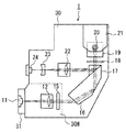
図1は、本発明の実施の形態の光ヘッド装置1を示す全体構成図である。
Hereinafter, embodiments of the present invention will be described with reference to the drawings.
[First Embodiment]
FIG. 1 is an overall configuration diagram showing an
この実施の形態の光ヘッド装置1は、例えば記録型のDVDを対象にその記録面にレーザ光を照射してデータの記録と再生を行うもので、図1に示すように、レーザ出力手段としての半導体レーザ11と、レーザ光を平行光にするコリメータレンズ12と、フォーカス制御やトラッキング制御用にレーザ光を複数のビームにする回折格子15と、光軸を曲げるプリズム16と、光ディスクへの進行ビームと光ディスクからの反射ビームとを分離するPBS(偏光ビームスプリッタ)17と、進行ビームと反射ビームの偏光を90度回転させる1/4波長板18と、立上げミラー19と、光ディスクの記録面にレーザ光を集束させる対物レンズ20と、この対物レンズ20をフォーカス方向やトラッキング方向に駆動する対物レンズ駆動装置21と、PBS17により分離された反射ビームを集束させるレンズ22と、この反射ビームにフォーカス制御やトラッキング制御のために非点収差を与える凹型の円筒レンズ23と、反射ビームの強度を検出する8分割センサ24等を備えている。
An
光ヘッド装置1の機枠は、例えば亜鉛ダイカストからなり半導体レーザ11以外の光学系部品が取り付けられるベースフレーム30と、例えばアルミ成型部材からなり半導体レーザ11が取り付けられてその放熱板としての機能を有するサブフレーム31とからなる。
The machine frame of the
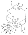
図2には、光ヘッド装置1の半導体レーザ11の取付け構造を示す分離斜視図を、図3には半導体レーザ11の位置調整を行っているところの正面図を、それぞれ示す。
FIG. 2 is an exploded perspective view showing the mounting structure of the
ベースフレーム30は、サブフレーム31との接合面30Cが平面状に形成され、且つ、この接合面30Cにダイヤモンド・ライク・カーボン(DLC)膜が形成されている。また、この接合面30Cには、レーザー光を通過させる光路用の孔30aやサブフレーム31をネジ止着するためのネジ穴30b,30bが設けられている。
The
サブフレーム31は、ベースフレーム30との接合面31Cが平面状にされた板状ブロックの形状に成型され、且つ、この接合面31Cにダイヤモンド・ライク・カーボン(DLC)膜が形成されている。また、サブフレーム31には、半導体レーザ11を固定する固定用溝31aやネジ止着用の挿通孔31b,31b、並びに、位置調整用ジグのアームF,Fに挟持されるための係合溝31d,31dが設けられている。
The
半導体レーザ11は、サブフレーム31の固定用溝31aに嵌合されて、例えば接着剤等により固着される。そして、このサブフレーム31がその接合面31Cをベースフレーム30の接合面30Cに重ね合わされた状態でベースフレーム30にネジ止着されて固定されるようになっている。
The
ネジ止着する前には、図3に示すように、サブフレーム31は位置調整用ジグの可動アームF,Fに強固に挟持され、且つ、サブフレーム31がベースフレーム30に或る程度の力で押圧された状態で、可動アームF,Fが光軸と直行するXY方向に動いて半導体レーザの位置を最適化し、その上でネジ止着が行われるようになっている。位置調整のときにサブフレーム31をベースフレーム30に或る程度押圧させた状態にするのは、ネジを止着するときにサブフレーム31とベースフレーム30とが位置ずれするのを防ぐためである。
Before the screws are fastened, as shown in FIG. 3, the
この実施の形態の光ヘッド装置1によれば、ベースフレーム30とサブフレーム31の接合面30C,31Cにダイヤモンド・ライク・カーボン(DLC)膜が形成されているので、半導体レーザ11の位置調整の際にサブフレーム31をベースフレーム30に強く押圧しても、DLC膜により低摩擦の摺動性が得られる。そして、それにより、位置調整用ジグの可動アームF,FをXY方向にスムースに移動させることができ、半導体レーザ11の正確な位置合わせができる。
According to the
また、厚みを有するフッ素樹脂膜を間に挿んだものに比べて、ネジも強固に止着できるのでベースフレーム30とサブフレーム31の固定を強固に行うことが出来る。
Further, since the screws can be firmly fixed as compared with the case where a fluororesin film having a thickness is inserted therebetween, the
また、DLC膜によりサブフレーム31とベースフレーム30との接合面30C,31Cにカジリが生じることが少ない。従って、使用劣化で半導体レーザ11を交換する場合や、製品のアセンブリ工程で半導体レーザ11の固定後に半導体レーザ11やその固定位置に不良が検出された場合でも、サブフレーム31をベースフレーム30から取り外して、同様の方法で、再び半導体レーザ11を取り付けることが出来る。
[第2の実施の形態]
第2の実施の形態は、ベースフレーム30とサブフレーム31の接合部分にグラファイト板を貼り付けて、各接合面30C,31Cをグラファイト面により構成するとともに、サブフレーム31をベースフレーム30に固定する際に、各接合面30C,31Cの間にフラーレン・ゲル状体(すなわちフラーレンをコロイド溶液中に添加してゲル状としたもの)を塗布したものである。
Further, the DLC film hardly causes galling on the joint surfaces 30C and 31C between the
[Second Embodiment]
In the second embodiment, a graphite plate is affixed to the joining portion of the
このような構成においても、ベースフレーム30とサブフレーム31の各接合面30C,31Cに低摩擦の摺動性を得ることが出来るとともに、ベースフレーム30とサブフレーム31の互いの接合面を強く押し付けてもカジリなどを生じ難くすることが出来る。従って、第1の実施の形態と同様の効果を得ることが出来る。
Even in such a configuration, it is possible to obtain low-friction slidability on the joint surfaces 30C and 31C of the
なお、上記のフラーレン・ゲル状体はシリコンオイルなどにフラーレンを添加してなるゾル状体などとしても良い。
[第3の実施の形態]
第3の実施の形態は、ベースフレーム30のサブフレーム31と接合す一区画(例えば図1の点線の区画)30Hをフェライトなどのモース硬度が6以上の部材で構成する一方、サブフレーム31をダイヤモンド・ライク・カーボンなどモース硬度が9以上の部材で構成したものである。
The fullerene / gel-like material may be a sol-like material obtained by adding fullerene to silicon oil or the like.
[Third Embodiment]
In the third embodiment, one section (for example, a dotted line section in FIG. 1) 30H joined to the
このような構成においても、ベースフレーム30とサブフレーム31の各接合面30C,31Cに低摩擦の摺動性を得ることが出来るとともに、ベースフレーム30とサブフレーム31の接合面30C,31Cを互いに強く押し付けてもカジリなどを生じ難くすることが出来る。そして、それにより、第1の実施の形態と同様の効果を得ることが出来る。
Even in such a configuration, it is possible to obtain low-friction slidability on the joint surfaces 30C and 31C of the
なお、モース硬度6以上の部材としては、その他、長石、石英、ガラスなどを適用することが出来る。また、上記構成では、ベースフレーム30の方を6以上のモース硬度で、サブフレーム31の方を9以上のモース硬度にすると説明したが、逆にベースフレーム30の方を9以上のモース硬度で、サブフレーム31の方を6以上のモース硬度にしても同様の作用・効果が奏される。
In addition, as a member having a Mohs hardness of 6 or more, feldspar, quartz, glass, or the like can be applied. In the above configuration, the
なお、本発明は、上記の実施の形態に限られるものではなく、例えば、上記の第1と第2の実施の形態において、ベースフレーム30とサブフレーム31の両方の接合面30C,31Cについて、DLC膜を形成するか、或いは、グラファイト板を貼り付けると説明したが、何れか一方の接合面についてのみこのような構成としても完全ではないが同様の効果を奏すことが出来る。
The present invention is not limited to the above embodiment. For example, in the first and second embodiments described above, the joint surfaces 30C and 31C of both the
また、ベースフレーム30とサブフレーム31の接合面の構成として第1〜第3の実施形態を示したが、その他、この接合面にテフロン(登録商標)粒子やダイフロン粒子が添加された潤滑剤を塗布するようにしても、接合面における低摩擦の摺動性と、接合面においてカジリを生じにくくするという作用を得ることが出来る。
In addition, the first to third embodiments have been described as the configuration of the joint surface between the
その他、サブフレーム31の形状やその位置調整方法など、実施の形態で具体的に示した細部構造および方法は一例に過ぎず、種々の変形がありえる。
In addition, the detailed structure and method specifically shown in the embodiment, such as the shape of the
また、光ヘッド装置を構成する光学系の種類や配置は種々の変更が可能であるし、また、光ヘッド装置が対象とする光ディスクの種類も記録型のDVDに限られず、種々の光ディスクを対象とするものでも良い。 In addition, the type and arrangement of the optical system constituting the optical head device can be variously changed, and the type of the optical disk targeted by the optical head device is not limited to the recordable DVD, but targets various optical disks. It may be.
1 光ヘッド装置
11 半導体レーザ
12 コリメータレンズ
15 回折格子
16 プリズム
17 PBS
18 1/4波長板
19 立上げミラー
20 対物レンズ
21 対物レンズ駆動装置
22 集束レンズ
23 円筒レンズ
24 光センサ
30 ベースフレーム
30C 接合面
31 サブフレーム
31C 接合面
DESCRIPTION OF
18 1/4
Claims (4)
亜鉛ダイカストにより形成されレーザ光を光ディスクに導く光学系が取り付けられるベースフレームと、
アルミ成型部材からなりレーザ光を出力するレーザ出力素子が取り付けられて上記ベースフレームに固定されるサブフレームとを備え、
上記ベースフレームと上記サブフレームの接合面の両方にダイヤモンド・ライク・カーボン膜が形成されていることを特徴とする光ヘッド装置。 In an optical head device that records or reproduces data by irradiating a recording surface of an optical disc with a laser beam,
A base frame to which an optical system that is formed by zinc die casting and guides laser light to an optical disk is attached;
A laser output element made of an aluminum molded member and attached with a laser output element for outputting laser light and fixed to the base frame;
An optical head device, characterized in that a diamond-like carbon film is formed on both of the joining surfaces of the base frame and the subframe.
亜鉛ダイカストにより形成されレーザ光を光ディスクに導く光学系が取り付けられるベースフレームと、
アルミ成型部材からなりレーザ光を出力するレーザ出力素子が取り付けられて上記ベースフレームに固定されるサブフレームとを備え、
上記ベースフレームと上記サブフレームの接合面の両方にグラファイト板が貼り付けられ、且つ、この接合面にフラーレン・ゲル状体或いはフラーレン・ゾル状体が塗布されていることを特徴とする光ヘッド装置。 In an optical head device that records or reproduces data by irradiating a recording surface of an optical disc with a laser beam,
A base frame to which an optical system that is formed by zinc die casting and guides laser light to an optical disk is attached;
A laser output element made of an aluminum molded member and attached with a laser output element for outputting laser light and fixed to the base frame;
An optical head device in which a graphite plate is attached to both the joint surfaces of the base frame and the sub-frame, and a fullerene / gel-like body or a fullerene / sol-like body is applied to the joint surface. .
亜鉛ダイカストにより形成されレーザ光を光ディスクに導く光学系が取り付けられるベースフレームと、
アルミ成型部材からなりレーザ光を出力するレーザ出力素子が取り付けられて上記ベースフレームに固定されるサブフレームとを備え、
上記ベースフレームと上記サブフレームの接合面の両方にグラファイト板が貼り付けられ、且つ、この接合面にパーフロロ系フッ素樹脂の微粒子を含んだ潤滑剤が塗布されていることを特徴とする光ヘッド装置。 In an optical head device that records or reproduces data by irradiating a recording surface of an optical disc with a laser beam,
A base frame to which an optical system that is formed by zinc die casting and guides laser light to an optical disk is attached;
A laser output element made of an aluminum molded member and attached with a laser output element for outputting laser light and fixed to the base frame;
An optical head device characterized in that a graphite plate is attached to both of the joining surfaces of the base frame and the sub frame, and a lubricant containing fine particles of perfluoro fluororesin is applied to the joining surfaces. .
Priority Applications (2)
| Application Number | Priority Date | Filing Date | Title |
|---|---|---|---|
| JP2003381980A JP4032425B2 (en) | 2003-11-12 | 2003-11-12 | Optical head device |
| US10/985,040 US7366062B2 (en) | 2003-11-12 | 2004-11-10 | Optical head disk device |
Applications Claiming Priority (1)
| Application Number | Priority Date | Filing Date | Title |
|---|---|---|---|
| JP2003381980A JP4032425B2 (en) | 2003-11-12 | 2003-11-12 | Optical head device |
Publications (2)
| Publication Number | Publication Date |
|---|---|
| JP2005149565A JP2005149565A (en) | 2005-06-09 |
| JP4032425B2 true JP4032425B2 (en) | 2008-01-16 |
Family
ID=34616095
Family Applications (1)
| Application Number | Title | Priority Date | Filing Date |
|---|---|---|---|
| JP2003381980A Expired - Fee Related JP4032425B2 (en) | 2003-11-12 | 2003-11-12 | Optical head device |
Country Status (2)
| Country | Link |
|---|---|
| US (1) | US7366062B2 (en) |
| JP (1) | JP4032425B2 (en) |
Families Citing this family (4)
| Publication number | Priority date | Publication date | Assignee | Title |
|---|---|---|---|---|
| JP4770715B2 (en) * | 2006-11-20 | 2011-09-14 | 船井電機株式会社 | Optical pickup device |
| JP2008152888A (en) * | 2006-12-20 | 2008-07-03 | Funai Electric Co Ltd | Objective lens driving device, assembling method for the same and optical disk apparatus |
| JP5152923B2 (en) * | 2009-02-13 | 2013-02-27 | 京セラドキュメントソリューションズ株式会社 | Inkjet recording apparatus and inkjet recording method |
| CN106163649A (en) * | 2014-04-10 | 2016-11-23 | 国际壳牌研究有限公司 | The method manufacturing support type gas separation membrane |
Family Cites Families (4)
| Publication number | Priority date | Publication date | Assignee | Title |
|---|---|---|---|---|
| JPH03165321A (en) | 1989-11-24 | 1991-07-17 | Ricoh Co Ltd | parts assembly structure |
| JP2002269791A (en) * | 2001-03-15 | 2002-09-20 | Sankyo Seiki Mfg Co Ltd | Optical head device |
| US6968563B2 (en) * | 2001-07-27 | 2005-11-22 | Kabushiki Kaisha Toshiba | Optical head |
| JP2005276242A (en) * | 2004-03-22 | 2005-10-06 | Pioneer Electronic Corp | Disk drive unit |
-
2003
- 2003-11-12 JP JP2003381980A patent/JP4032425B2/en not_active Expired - Fee Related
-
2004
- 2004-11-10 US US10/985,040 patent/US7366062B2/en not_active Expired - Fee Related
Also Published As
| Publication number | Publication date |
|---|---|
| US20050120363A1 (en) | 2005-06-02 |
| JP2005149565A (en) | 2005-06-09 |
| US7366062B2 (en) | 2008-04-29 |
Similar Documents
| Publication | Publication Date | Title |
|---|---|---|
| US7457055B2 (en) | Lens driving apparatus and optical pickup unit having the same | |
| US20080310287A1 (en) | Deformable mirror apparatus, optical pickup and optical drive apparatus | |
| US20080212214A1 (en) | Fixing structure of optical element | |
| JP4032425B2 (en) | Optical head device | |
| WO2003102940A1 (en) | Lens support mechanism, optical head device and optical information processor | |
| EP1178474A1 (en) | Optical head | |
| JPH09274123A (en) | Optical element fixing device | |
| JP2006099875A (en) | Positioning fixed structure for beam shaping prism | |
| JP3980528B2 (en) | Optical pickup | |
| JP3991227B2 (en) | Optical head device | |
| JP4785695B2 (en) | Optical pickup device | |
| JP2008171498A (en) | Optical head device | |
| JPH087313A (en) | Optical head | |
| JP4947940B2 (en) | Optical pickup device | |
| JPH10255318A (en) | Integrated optical unit | |
| JP2003187461A (en) | Optical pickup | |
| JP2005285166A (en) | Optical pickup device | |
| JP3882937B2 (en) | Optical pickup | |
| JP2004281033A (en) | Optical pickup | |
| JP2008103014A (en) | Mounting method of optical component and optical pickup | |
| JP2007157293A (en) | Structure of mounting launch mirror on base member | |
| JP2004145976A (en) | Optical head device | |
| JPH03165321A (en) | parts assembly structure | |
| JP2009064485A (en) | Optical pickup device | |
| JP2005332448A (en) | Optical recording medium fixing apparatus, optical recording medium fixing method, and optical recording / reproducing apparatus |
Legal Events
| Date | Code | Title | Description |
|---|---|---|---|
| A977 | Report on retrieval |
Free format text: JAPANESE INTERMEDIATE CODE: A971007 Effective date: 20060630 |
|
| A131 | Notification of reasons for refusal |
Free format text: JAPANESE INTERMEDIATE CODE: A131 Effective date: 20060724 |
|
| A521 | Written amendment |
Free format text: JAPANESE INTERMEDIATE CODE: A523 Effective date: 20060922 |
|
| TRDD | Decision of grant or rejection written | ||
| A01 | Written decision to grant a patent or to grant a registration (utility model) |
Free format text: JAPANESE INTERMEDIATE CODE: A01 Effective date: 20071001 |
|
| A61 | First payment of annual fees (during grant procedure) |
Free format text: JAPANESE INTERMEDIATE CODE: A61 Effective date: 20071014 |
|
| FPAY | Renewal fee payment (event date is renewal date of database) |
Free format text: PAYMENT UNTIL: 20101102 Year of fee payment: 3 |
|
| R150 | Certificate of patent or registration of utility model |
Free format text: JAPANESE INTERMEDIATE CODE: R150 |
|
| FPAY | Renewal fee payment (event date is renewal date of database) |
Free format text: PAYMENT UNTIL: 20111102 Year of fee payment: 4 |
|
| FPAY | Renewal fee payment (event date is renewal date of database) |
Free format text: PAYMENT UNTIL: 20111102 Year of fee payment: 4 |
|
| FPAY | Renewal fee payment (event date is renewal date of database) |
Free format text: PAYMENT UNTIL: 20121102 Year of fee payment: 5 |
|
| FPAY | Renewal fee payment (event date is renewal date of database) |
Free format text: PAYMENT UNTIL: 20121102 Year of fee payment: 5 |
|
| FPAY | Renewal fee payment (event date is renewal date of database) |
Free format text: PAYMENT UNTIL: 20131102 Year of fee payment: 6 |
|
| LAPS | Cancellation because of no payment of annual fees |