JP4031389B2 - Image conversion apparatus and image conversion method - Google Patents
Image conversion apparatus and image conversion method Download PDFInfo
- Publication number
- JP4031389B2 JP4031389B2 JP2003107139A JP2003107139A JP4031389B2 JP 4031389 B2 JP4031389 B2 JP 4031389B2 JP 2003107139 A JP2003107139 A JP 2003107139A JP 2003107139 A JP2003107139 A JP 2003107139A JP 4031389 B2 JP4031389 B2 JP 4031389B2
- Authority
- JP
- Japan
- Prior art keywords
- signal
- progressive
- circuit
- interlaced video
- value
- Prior art date
- Legal status (The legal status is an assumption and is not a legal conclusion. Google has not performed a legal analysis and makes no representation as to the accuracy of the status listed.)
- Expired - Fee Related
Links
Images


Classifications
-
- H—ELECTRICITY
- H04—ELECTRIC COMMUNICATION TECHNIQUE
- H04N—PICTORIAL COMMUNICATION, e.g. TELEVISION
- H04N7/00—Television systems
- H04N7/01—Conversion of standards, e.g. involving analogue television standards or digital television standards processed at pixel level
-
- H—ELECTRICITY
- H04—ELECTRIC COMMUNICATION TECHNIQUE
- H04N—PICTORIAL COMMUNICATION, e.g. TELEVISION
- H04N7/00—Television systems
- H04N7/01—Conversion of standards, e.g. involving analogue television standards or digital television standards processed at pixel level
- H04N7/0117—Conversion of standards, e.g. involving analogue television standards or digital television standards processed at pixel level involving conversion of the spatial resolution of the incoming video signal
- H04N7/012—Conversion between an interlaced and a progressive signal
-
- H—ELECTRICITY
- H04—ELECTRIC COMMUNICATION TECHNIQUE
- H04N—PICTORIAL COMMUNICATION, e.g. TELEVISION
- H04N7/00—Television systems
- H04N7/01—Conversion of standards, e.g. involving analogue television standards or digital television standards processed at pixel level
- H04N7/0135—Conversion of standards, e.g. involving analogue television standards or digital television standards processed at pixel level involving interpolation processes
- H04N7/0137—Conversion of standards, e.g. involving analogue television standards or digital television standards processed at pixel level involving interpolation processes dependent on presence/absence of motion, e.g. of motion zones
-
- H—ELECTRICITY
- H04—ELECTRIC COMMUNICATION TECHNIQUE
- H04N—PICTORIAL COMMUNICATION, e.g. TELEVISION
- H04N5/00—Details of television systems
- H04N5/14—Picture signal circuitry for video frequency region
- H04N5/144—Movement detection
Description
【0001】
【発明の属する技術分野】
本発明は、インタレース映像信号をプログレッシブ映像信号に変換する画像変換装置および画像変換方法に関する。
【0002】
【従来の技術】
従来、インタレース映像信号をプログレッシブ映像信号に変換するために、動き適応型プログレッシブ変換装置が用いられていた(例えば、特許文献1参照)。
【0003】
図14は、インタレース映像信号の一例を示す。1フレームのインタレース映像信号は、2フィールドの画像として伝送される。例えば、Lがある偶数の値の場合において、NフィールドでLライン、L+2ライン、L+4ライン、L+6ライン、L+8ライン等の偶数番目のラインの信号が伝送される。続いて、N+1フィールドでは、L+1ライン、L+3ライン、L+5ライン、L+7ライン等の奇数番目のラインの信号が伝送される。さらに次のN+2フィールドでは、Nフィールドと同じ偶数番目のラインの信号が伝送される。
【0004】
このように、インタレース映像信号は、2フィールドに分けて伝送され、これらの2フィールドの走査線によって1フレームの映像が表示される。
【0005】
各フィールドにおいて伝送されていないラインの信号は、時間的に前後のフィールドまたは現フィールドの信号(例えば上下のラインの信号)から生成される。その信号と伝送される信号とが合成されることにより、プログレッシブ映像信号が形成される。
【0006】
以下、現フィールドで実際に送られているラインを現ラインと呼び、時間的に前後の複数のフィールドから、または、現フィールドの信号から生成されたラインを補間ラインと呼ぶ。
【0007】
図15は、従来の動き適応型プログレッシブ変換装置の一構成例を示す。図15に示すように、動き適応型プログレッシブ変換装置は、1フィールド遅延回路J1,J2、動き検出回路J3、フレーム間補間回路J4、フィールド内補間回路J5、切り換え回路J6を備える。インタレース映像信号J0は、1フィールド遅延回路J1および1フィールド遅延回路J2でそれぞれ1フィールドずつ遅延される。
【0008】
動き検出回路J3は、時間的に2フィールド前または後のフィールド同士の間(以下、これをフレーム間と呼ぶ)の同一ライン上の対応する画素の比較を行う。動き検出回路J3は、比較した画素の値の差が小さい場合はそれらの画素を「静止画」と判定し、比較した画素の値の差が大きい場合はそれらの画素を「動画」と判定する。
【0009】
フレーム間補間回路J4は、フレーム間の同一ライン上の画素から対応する画素を生成する。例えば、図14において、N+1フィールドのL+4ラインの画素Xを補間する場合は、フレーム間補間回路J4は、NフィールドのL+4ラインの画素AとN+2フィールドのL+4ラインの画素Bとから、例えば「X=(A+B)/2」(A,Bは画素の信号の明るさのレベルを示す)という演算によって画素Xを生成する。
【0010】
フィールド内補間回路J5は、同一フィールド内の隣接するラインの画素から対応する画素を生成する。例えば、図14において、N+1フィールドのL+4ラインの画素Xを補間する場合は、フィールド内補間回路J5は、N+1フィールドのL+3ラインの画素CとN+1フィールドのL+5ラインの画素Dとから、例えば「X=(C+D)/2」(C,Dは画素の信号の明るさのレベルを示す)という演算によって画素Xを生成する。
【0011】
切り換え回路J6は、1フィールド遅延回路J1の出力が現ラインである場合には、この現ライン信号を選択してプログレッシブ映像信号J7として出力する。切り換え回路J6は、動き検出回路J3が注目画素を「静止画」と判定すればフレーム間補間回路J4から与えられる信号をプログレッシブ映像信号J7として出力し、動き検出回路J3が注目画素を「動画」と判定すればフィールド内補間回路J5から与えられる生成信号をプログレッシブ映像信号J7として出力する。
【0012】
このような構成の装置であれば、フレーム間で相関の大きい静止画については、フレーム間補間(時間的に2つ前または後のフィールドからなされる補間)によって生成されたプログレッシブ映像信号が出力される。一方、フレーム間で相関性の小さい動画については、フィールド内補間によって生成されたプログレッシブ映像信号が出力される。したがって、この方法によれば、理論上は、画像の動きにほぼ合致した補間処理が可能となるはずである。
【0013】
【特許文献1】
特開平10−112845号公報
【0014】
【発明が解決しようとする課題】
しかしながら、従来例のような方法では垂直方向に大きな輝度差を持つ画像がゆっくり動いたときに正確な判定ができないことから、静止画に適したフレーム間補間処理と動画に適したフィールド内補間処理がうまく行われずに画像が劣化する場合がある。
【0015】
このような場合の例を以下に示す。図16は、インタレース映像信号に変換される前の元となる映像信号を示す。この映像信号は、正弦波的に明るさの度合い(輝度)が変化する。縦軸は輝度を表し、横軸はラインの番号を表している。黒の輝度は最低の値「0」とし、白の輝度は最大の値「255」として表示されている。図中の数値はサンプリング後のサンプル値を示す。
【0016】
元となる映像信号の輝度は、Lラインで値「218」となり、LラインとL+1ラインとの間で値「255」の最大輝度となり、L+1ラインで値「218」となり、L+1ラインとL+2ラインの間で値「128」となり、L+2ラインで値「37」となり、L+2ラインとL+3との間で値「0」の最小輝度となり、L+3ラインで値「37」となり、L+3ラインとL+4ラインの間で値「128」となり、L+4ラインで値「218」となる。以下、同様にL+5ライン以降も変化している。この画像がインタレース映像信号として伝送された場合は、図17のようになる。つまり、あるフィールドでは黒丸の値が伝送され、次のフィールドでは白丸の値が伝送される。
【0017】
図18は、このようなインタレース映像信号が1フィールドごとに1/2ラインずつ動いたときの映像信号を重ねたものである。すなわち、f1フィールドでは、Lラインとして値「218」、L+2ラインとして値「37」、L+4ラインとして値「218」、L+6ラインとして値「37」のそれぞれの輝度が伝送される。
【0018】
続いて、f2フィールドでは元の映像信号の波形が1/2ラインずつ動いているため、L+1ラインとして値「255」、L+3ラインとして値「0」、L+5ラインとして値「255」、L+7ラインとして値「0」が伝送される。以下、f3フィールド、f4フィールド、f5フィールドおよびf6フィールドではそれぞれ図のように映像信号の輝度値が伝送される。このような各フィールドでのラインとサンプル値の関係を表1に示す。
【0019】
【表1】

表1(a)は、各フィールドにおいてインタレース映像信号としてサンプリングされる前の元となる映像信号の輝度値を示し、表1(b)はインタレース映像信号としてサンプリングされた後の映像信号の輝度値を示している。このインタレース映像信号をうけた受信機側で補間信号処理されて伝送されないライン、すなわち表1(b)の「−」欄の輝度値が求められ、プログレッシブ映像信号に変換される。
【0021】
このようなインタレース映像信号が図15に示す従来の動き適応型プログレッシブ変換装置で処理される場合の動作について説明する。従来の動き適応型プログレッシブ変換装置では、動き検出回路J3は、あるフィールドのインタレース映像信号の輝度値と時間的に2フィールド後または前のフィールドのインタレース映像信号との輝度値の差により、注目画素が「静止画」であるか「動画」であるかを判定する。その判定結果は切り換え回路J6へ送られる。
【0022】
切り換え回路J6は、動き検出回路J3による判定結果が「静止画」であればフレーム間補間回路J4から与えられる信号をプログレッシブ映像信号J7として出力する。また、動き検出回路J3による判定結果が「動画」であればフィールド内補間回路J5から与えられる信号をプログレッシブ映像信号J7として出力する。
【0023】
まず、動き検出回路J3の動作を表2(a)、表2(b)を用いて説明する。
【0024】
【表2】
表2(a)は、あるフィールドのインタレース映像信号の輝度値と2フィールド後または前のフィールドのインタレース映像信号の輝度値との差を示している。表2(a)の値は動き検出回路J3によって演算されたものである。例えば、f2フィールドのLラインの輝度値は、f1フィールドのLラインの値「218」とf3フィールドのLラインの値「37」との差をとって値「181」となっている。同様に各フィールドの各ラインの輝度値が演算されている。
【0026】
表2(b)は、表2(a)の輝度値をもとにして動き検出回路J3が注目画素が「動画」であるかまたは「静止画」であるかを判定した結果である。ここでは、動画と静止画の明るさの閾値を値「20」とする。閾値「20」以上の場合は動き検出回路J3は注目画素を「動画」と判定し、「19」以下の場合は動き検出回路J3は注目画素を「静止画」と判定する。
【0027】
次に、フレーム間補間回路J4およびフィールド内補間回路J5の動作を説明する。
【0028】
【表3】
表3(a)はフレーム間補間回路J4の出力値を示したものである。例えば、映像入力がf2フィールドのLラインにおいては、インタレース映像信号では実際には伝送されず、フレーム間での補間信号処理により求められる。そこでフレーム間補間回路J4でのf2フィールドのLラインの輝度値は、表1(b)のf1フィールドのLラインの値「218」とf3フィールドのLラインの値「37」とで平均をとり、つまり「(218+37)/2=128」として計算されている。表3(a)のその他の輝度値も同様にしてフレーム間の輝度値の平均として算出されている。
【0030】
一方、表3(b)はフィールド内補間回路J5の出力値を示したものである。例えばf1フィールドのL+1ラインの輝度値をフィールド間での補間処理を行う場合、表1(b)のf1フィールドのLラインの値「218」と同じf1フィールドのL+2ラインの値「37」から平均が求められ、「(218+37)/2=128」と計算されている。表3(b)のその他の輝度値も同様にして、フィールド内の上下ラインの値の平均として算出されている。
【0031】
次に、切り換え回路J6の動作を説明する。切り換え回路J6には、フレーム間補間回路J4から与えられる信号と、フィールド内補間回路J5から与えられる信号と、現ライン信号と、さらに動き検出回路J3から与えられる信号とが与えられる。
【0032】
次の表4は、切り換え回路J6から出力されるプログレッシブ映像信号J7の信号の輝度値を示すものである。
【0033】
【表4】
表4(a)は、表2(b)の動き検出回路J3の判定結果によって、フレーム間補間信号とフィールド内補間信号を切り換えて出力した結果を示している。動き検出回路J3が注目画素を「静止画」と判定すればフレーム間補間回路J4が生成した信号を出力し、動き検出回路J3が注目画素を「動画」と判定すればフィールド内補間回路J5が生成した信号を出力する。
【0035】
表4(a)においてハッチングがなされている部分が「動画」と判定された部分である。なお、表4(a)の「−」の箇所は、現ラインのインタレース映像信号が出力されていることを示す。
【0036】
表4(b)は、補間ラインで出力された信号の輝度値と、表1(a)のインタレースされる前の元となる映像信号の輝度値との差を示したものである。この表4(b)からわかるようにf3フィールドおよびf5フィールドにおいて、その輝度の差が値「90」であり、非常に大きくなっていることが判る。これらの信号の最大値が値「255」であるのに対して、値「90」という値は非常に大きく、プログレッシブ変換されたプログレッシブ映像信号を見ても大きなノイズとなってしまい、顕著な画質劣化として認識される。
【0037】
このように、従来の動き適応型プログレッシブ変換装置では、画像がゆっくりとライン方向に対して垂直に動いたときには動き検出回路J3が注目画素を「動画」と判定しやすく、画質が劣化しやすいという課題があった。
【0038】
本発明の目的は、垂直方向に大きな輝度差を持つ画像がゆっくり動いたときにおいても、正確な動き判定を行い、インタレース映像信号を安定で解像度の高いプログレッシブ映像信号に変換する画像変換装置を提供することである。
【0039】
【課題を解決するための手段】
第1の発明に係る画像変換装置は、入力されたインタレース映像信号をプログレッシブ映像信号に変換する画像変換装置であって、入力されたインタレース映像信号に基づく演算によりプログレッシブ信号を生成するプログレッシブ信号生成回路と、プログレッシブ信号生成回路により生成された前記プログレッシブ信号に基づいて画像の垂直方向の動き量を算出する動き算出回路と、入力されたインタレース映像信号から静止画処理によって静止画プログレッシブ信号を生成する静止画処理回路と、入力されたインタレース映像信号から動画処理によって動画プログレッシブ信号を生成する動画処理回路と、動き算出回路により算出された垂直方向の動き量が第1の値より小さい場合に静止画処理回路により出力される静止画プログレッシブ信号を出力する出力回路とを備え、プログレッシブ信号生成回路は、入力されたインタレース映像信号に基づいて、連続する複数のフィールドにそれぞれ対応する複数のインタレース映像信号を生成するインタレース生成回路と、インタレース生成回路により生成された複数のインタレース映像信号のうち第1の組み合わせの複数のインタレース映像信号に基づいて第1のプログレッシブ信号を生成する第1のプログレッシブ回路と、インタレース生成回路により生成された複数のインタレース映像信号のうち第1の組み合わせと異なる第2の組み合わせの複数のインタレース映像信号に基づいて第2のプログレッシブ信号を生成する第2のプログレッシブ回路とを含み、動き算出回路は、第1のプログレッシブ生成回路により生成された第1のプログレッシブ信号および第2のプログレッシブ生成回路により生成された第2のプログレッシブ信号に基づいて動き量を算出し、出力回路は、動き量がライン間の間隔以下である場合に静止画プログレッシブ信号の割合を0.5以上にするものである。
第2の発明に係る画像変換装置は、入力されたインタレース映像信号をプログレッシブ映像信号に変換する画像変換装置であって、入力されたインタレース映像信号に基づく演算によりプログレッシブ信号を生成するプログレッシブ信号生成回路と、プログレッシブ信号生成回路により生成された前記プログレッシブ信号に基づいて画像の垂直方向の動き量を算出する動き算出回路と、入力されたインタレース映像信号から静止画処理によって静止画プログレッシブ信号を生成する静止画処理回路と、入力されたインタレース映像信号から動画処理によって動画プログレッシブ信号を生成する動画処理回路と、動き算出回路により算出された垂直方向の動き量が第1の値より小さい場合に静止画処理回路により出力される静止画プログレッシブ信号を出力する出力回路と、複数のフィールドに対応する複数のインタレース映像信号における注目画素およびその周辺の画素の値の平均値をそれぞれ算出し、算出された平均値に基づいて静止画プログレッシブ信号の適用または非適用を判定する判定回路とを備え、プログレッシブ信号生成回路は、入力されたインタレース映像信号に基づいて、連続する複数のフィールドにそれぞれ対応する複数のインタレース映像信号を生成するインタレース生成回路と、インタレース生成回路により生成された複数のインタレース映像信号のうち第1の組み合わせの複数のインタレース映像信号に基づいて第1のプログレッシブ信号を生成する第1のプログレッシブ回路と、インタレース生成回路により生成された複数のインタレース映像信号のうち第1の組み合わせと異なる第2の組み合わせの複数のインタレース映像信号に基づいて第2のプログレッシブ信号を生成する第2のプログレッシブ回路とを含み、動き算出回路は、第1のプログレッシブ生成回路により生成された第1のプログレッシブ信号および第2のプログレッシブ生成回路により生成された第2のプログレッシブ信号に基づいて動き量を算出し、出力回路は、判定回路の判定結果が非適用の場合に動画プログレッシブ信号をプログレッシブ映像信号として出力し、判定回路は、複数のフィールドに対応する複数のインタレース映像信号の注目画素およびその周辺の画素の値の最大値および最小値をそれぞれ算出し、算出された平均値、最大値および最小値に基づいて静止画プログレッシブ信号の適用または非適用を判定するものである。
第3の発明に係る画像変換装置は、入力されたインタレース映像信号をプログレッシブ映像信号に変換する画像変換装置であって、入力されたインタレース映像信号に基づく演 算によりプログレッシブ信号を生成するプログレッシブ信号生成回路と、プログレッシブ信号生成回路により生成された前記プログレッシブ信号に基づいて画像の垂直方向の動き量を算出する動き算出回路と、入力されたインタレース映像信号から静止画処理によって静止画プログレッシブ信号を生成する静止画処理回路と、入力されたインタレース映像信号から動画処理によって動画プログレッシブ信号を生成する動画処理回路と、動き算出回路により算出された垂直方向の動き量が第1の値より小さい場合に静止画処理回路により出力される静止画プログレッシブ信号を出力する出力回路と、複数のフィールドに対応する複数のインタレース映像信号における注目画素およびその周辺の画素の値の平均値をそれぞれ算出し、算出された平均値に基づいて静止画プログレッシブ信号の適用または非適用を判定する判定回路とを備え、プログレッシブ信号生成回路は、入力されたインタレース映像信号に基づいて、連続する複数のフィールドにそれぞれ対応する複数のインタレース映像信号を生成するインタレース生成回路と、インタレース生成回路により生成された複数のインタレース映像信号のうち第1の組み合わせの複数のインタレース映像信号に基づいて第1のプログレッシブ信号を生成する第1のプログレッシブ回路と、インタレース生成回路により生成された複数のインタレース映像信号のうち第1の組み合わせと異なる第2の組み合わせの複数のインタレース映像信号に基づいて第2のプログレッシブ信号を生成する第2のプログレッシブ回路とを含み、動き算出回路は、第1のプログレッシブ生成回路により生成された第1のプログレッシブ信号および第2のプログレッシブ生成回路により生成された第2のプログレッシブ信号に基づいて動き量を算出し、出力回路は、判定回路の判定結果が非適用の場合に動画プログレッシブ信号をプログレッシブ映像信号として出力し、判定回路は、算出された平均値のそれぞれの差が所定値より大きく、算出された同一フィールドの最大値と最小値との差のそれぞれの値が所定値より小さい場合に静止画プログレッシブ信号を非適用と判定するものである。
【0040】
本発明に係る画像変換装置においては、入力されたインタレース映像信号に基づいてプログレッシブ信号が生成され、プログレッシブ信号に基づいて画像の垂直方向の動き量が動き算出回路により算出される。
【0041】
また、入力されたインタレース映像信号から静止画処理によって静止画プログレッシブ信号が静止画処理回路により生成され、入力されたインタレース映像信号から動画処理によって動画プログレッシブ信号が動画処理回路により生成される。垂直方向の動き量が第1の値より小さい場合に静止画プログレッシブ信号が出力回路により出力される。
【0042】
この場合、プログレッシブ信号に基づいて動き量が算出されるため、より正確で緻密な動き量を算出することができる。したがって、垂直方向の大きな輝度差を持つ画像が1ライン以下でゆっくり動いた場合でも正確な動き量を算出して画像の動きを判定することができるので、安定で解像度の高い映像を提供することができる。
【0044】
また、第1のプログレッシブ信号と第2のプログレッシブ信号とに基づいて動き量が算出されるため、より正確で緻密な動き量を算出することができる。したがって、垂直方向の大きな輝度差を持つ画像が1ライン以下でゆっくり動いた場合でも正確な動き量を算出して画像の動きを判定することができるので、安定で解像度の高い映像を提供することができる。
第1の発明に係る画像変換装置では、動きの大きい画像に対しての誤動作を防止することができ、画質劣化の少ないプログレッシブ映像信号を生成することができる。
第2および第3の発明に係る画像変換装置では、複数のフィールドに対応する複数のインタレース映像信号における注目画素およびその周辺の画素の値の平均値に基づいて判定回路により静止画プログレッシブ信号の適用または非適用が判定され、判定回路の判定結果が非適用の場合に動画プログレッシブ信号がプログレッシブ映像信号として出力される。
したがって、フリッカ性の画像、例えば連続したカメラのフラッシュ等が含まれる画像に対しても、誤って静止画処理をしないようにすることができ、より精度の高いプログレッシブ映像信号を生成することができる。
また、判定回路は、複数のフィールドに対応する複数のインタレース映像信号における注目画素およびその周辺の画素の信号の値の平均値を検出している。その結果、回路規模を比較的小さくすることができる。
第2の発明に係る画像変換装置では、複数のフィールドに対応する複数のインタレース映像信号の注目画素およびその周辺の画素の値の平均値、最大値および最小値に基づいて静止画プログレッシブ信号の適用または非適用が判定される。したがって、より正確に静止画プログレッシブ信号の適用または非適用が判定される。
第3の発明に係る画像変換装置では、算出された平均値のそれぞれの差が所定値より大きく、算出された同一フィールドの最大値と最小値との差のそれぞれの値が所定値より小さい場合に静止画プログレッシブ信号が非適用と判定される。したがって、より正確に静止画プログレッシブ信号の適用または非適用が判定される。
【0045】
第1の値はライン間の間隔以下の値であってもよい。この場合、動き算出回路により算出された垂直方向の動き量がライン間の間隔以下の場合に静止画プログレッシブ信号がプログレッシブ映像信号として出力される。したがって、垂直方向に大きな輝度差を持つ画像がゆっくり動いたときにおいても、正確な動き判定を行い、インタレース映像信号を安定で解像度の高いプログレッシブ映像に変換することができる。
【0046】
動き算出回路は、ライン間の間隔よりも小さい単位で垂直方向の動き量を算出してもよい。この場合、正確な動き検出を行うことができ、垂直方向の大きな輝度差を持つ画像がゆっくり動いたときにおいても、正確な動き判定を行い、インタレース映像信号を安定で解像度の高いプログレッシブ映像に変換することができる。
【0047】
画像変換装置は、第1のプログレッシブ生成回路により生成された第1のプログレッシブ信号を用いた補間処理によりライン間の補間画素を生成し、第1のプログレッシブ信号における画素および補間画素を含む第1の補間信号を出力する第1の画素形成回路と、第2のプログレッシブ生成回路により生成された第2のプログレッシブ信号を用いた補間処理によりライン間の補間画素を生成し、第2のプログレッシブ信号における画素および補間画素を含む第2の補間信号を出力する第2の画素形成回路とをさらに備え、動き算出回路は、第1の画素形成回路から出力された第1の補間信号および第2の画素形成回路から出力された第2の補間信号に基づいて動き量を算出してもよい。
【0048】
この場合、第1のプログレッシブ生成回路により第1の組み合わせの複数のインタレース映像信号に基づいて第1のプログレッシブ信号が生成され、第2のプログレッシブ生成回路により第2の組み合わせの複数のインタレース映像信号に基づいて第2のプログレッシブ信号が生成される。
【0049】
また、第1の画素形成回路により第1のプログレッシブ信号における画素および補間画素を含む第1の補間信号が出力され、第2の画素形成回路により第2のプログレッシブ信号における画素および補間画素を含む第2の補間信号が出力され、動き算出回路により第1の補間信号および第2の補間信号から動き量が算出される。
【0050】
したがって、インタレース映像信号をプログレッシブ映像信号に変換する際に、より厳しい変換精度を要求される垂直方向における精度を上げることができ、水平方向において新たに画素を生成する回路を省略できるので、回路規模の増大を低く抑えることができ、低コストに高精度のプログレッシブ映像に変換することができる。
【0051】
出力回路は、動き量が第2の値より大きい場合に動画プログレッシブ信号をプログレッシブ映像信号として出力してもよい。この場合、動き算出回路により算出された垂直方向の動き量が第2の値より大きい場合に動画処理回路により出力される動画プログレッシブ信号がプログレッシブ映像信号として出力回路から出力される。
【0052】
したがって、垂直方向に大きな輝度差を持つ画像がゆっくり動いたときにおいても、正確な動き判定を行い、インタレール映像信号を安定で解像度の高いプログレッシブ映像に変換することができる。
【0053】
出力回路は、動き量が第1の値と第2の値との間にある場合、動き量に基づく割合で動画プログレッシブ信号と静止画プログレッシブ信号とを合成し、合成された信号をプログレッシブ映像信号として出力してもよい。
【0054】
この場合、動き量に応じて動画プログレッシブ信号と静止画プログレッシブ信号とからプログレッシブ映像信号が生成されるので、画質劣化の少ない、解像度の高いプログレッシブ映像信号を生成することが可能である。
【0056】
複数のインタレース映像信号は、連続する第1〜第4のフィールドに対応する第1〜第4のインタレース映像信号を含み、第1の組み合わせの複数のインタレース映像信号は、第1〜第3のインタレース映像信号を含み、第2の組み合わせの複数のインタレース映像信号は、第2〜第4のインタレース映像信号を含んでもよい。
【0057】
この場合、より正確な動き検出をすることができ、垂直方向に大きな輝度差を持つ画像がゆっくり動いたときにおいても、正確な動き判定をすることができ、安定で解像度の高い映像を影響することができる。
【0058】
第1のプログレッシブ生成回路により生成された第1のプログレッシブ信号は現ライン信号および補間ライン信号によって構成され、第1のプログレッシブ信号の現ライン信号は、第2のインタレース映像信号を用いて生成され、第1のプログレッシブ信号の補間ライン信号は、第1のインタレース映像信号と第3のインタレース映像信号との演算値を用いて生成され、第2のプログレッシブ生成回路により生成された第2のプログレッシブ信号は現ライン信号および補間ライン信号によって構成され、第2のプログレッシブ信号の現ライン信号は、第3のインタレース映像信号を用いて生成され、第2のプログレッシブ信号の補間ライン信号は、第2のインタレース映像信号と第4のインタレース映像信号との演算値を用いて生成されてもよい。
【0059】
この場合、インタレース映像信号に多少の動きがあったとしても、補間ラインには、第1と第3のインタレース映像信号の演算により、また第2と第3のインタレース映像信号の演算により、相対的な動き量がキャンセルしあうように働くため、画像に動きがあったとしても 「静止画」 、 「動画」 の判定を正確に行うことができ、高精度に画質を改善でき、より高画質なプログレッシブ映像信号を提供することができる。
【0060】
第1のインタレース映像信号と第3のインタレース映像信号との演算値は、第1および第3のインタレース映像信号の対応する画素とその周辺の画素との演算値であり、第2のインタレース映像信号と第4のインタレース映像信号との演算値は、第2および第4のインタレース映像信号の対応する画素とその周辺の画素との演算値であってもよい。
【0061】
この場合、複数のインタレース映像信号の対応する画素とその周辺の画素との演算値を用いるため、よりノイズに強く、より精度の高い第1プログレッシブ信号と第2のプログレッシブ信号を生成することができ、より高精度の動き検出を行うことができる。
【0062】
第1のインタレース映像信号と第3のインタレース映像信号との演算値は、第1および第3のインタレース映像信号の対応する画素の平均値であり、第2のインタレース映像信号と第4のインタレース映像信号との演算値は、第2および第4のインタレース映像信号の対応する画素の平均値であってもよい。
【0063】
この場合、演算が平均をとることから非常に簡単に演算を行うことができ、演算回路を小さな規模にとどめることができる。したがって、低コストで画像変換装置を提供することができる。
【0064】
動き算出回路は、第1のプログレッシブ生成回路により生成された第1のプログレッシブ信号と第2のプログレッシブ生成回路により生成された第2のプログレッシブ信号との間で注目画素の値を比較し、および、注目画素とその周辺の画素との値を比較し、その比較結果を動き量として出力してもよい。
【0065】
この場合、動き算出回路の比較が注目画素だけにとどまらず、その周辺の画素をも含むので、動き検出をより高精度で行うことができる。
【0066】
動き算出回路は、第2のプログレッシブ信号の補間ライン信号の注目画素の値と、注目画素に対応した第1のプログレッシブ信号の現ライン信号の画素の値と、現ライン信号の画素の上下の補間ライン信号の画素の値とを演算し、その演算結果を動き量として出力し、および/または、第1のプログレッシブ信号の補間ライン信号の注目画素の値と、注目画素に対応した第2のプログレッシブ信号の現ライン信号の画素の値と、現ライン信号の画素の上下の補間ライン信号の画素の値とを演算し、その演算結果を動き量として出力してもよい。
【0067】
この場合、動き量を演算する演算が、2つのプログレッシブ信号の注目画素とその上下の補間ラインの画素に限定されるので、演算量を少なく抑えることができ、コストを低減することが可能となる。
【0068】
画像変換装置は、第1のプログレッシブ生成回路により生成された第1のプログレッシブ信号を用いた補間処理によりライン間の補間画素を生成し、第1のプログレッシブ信号における画素および補間画素を含む第1の補間信号を出力する画素形成回路をさらに備え、動き算出回路は、第1の画素形成回路から出力された第1の補間信号および第2のプログレッシブ生成回路により生成された第2のプログレッシブ信号に基づいて画像の垂直方向の動き量を算出してもよい。
【0069】
この場合、第1の画素形成回路から出力された第1の補間信号および第2のプログレッシブ生成回路により生成された第2のプログレッシブ信号に基づいて画像の垂直方向の動き量が算出されるので、より精度の高い動き検出が可能になり、画質劣化の少ない、解像度の高いプログレッシブ映像フィールド信号を生成することが可能となる。
【0070】
また、インタレース映像信号をプログレッシブ映像信号に変換する際に、より厳しい変換精度を要求される垂直方向における精度を上げることができ、水平方向において新たに画素を生成する回路を省略できるので、さらに回路規模の増大を低く抑えることができ、低コストに高精度のプログレッシブ映像に変換することができる。
【0079】
第4の発明に係る画像変換方法は、入力されたインタレース映像信号をプログレッシブ映像信号に変換する画像変換方法であって、入力されたインタレース映像信号に基づく演算によりプログレッシブ信号を生成するステップと、生成されたプログレッシブ信号に基づいて画像の垂直方向の動き量を算出するステップと、入力されたインタレース映像信号から静止画処理によって静止画プログレッシブ信号を生成するステップと、入力されたインタレース映像信号から動画処理によって動画プログレッシブ信号を生成するステップと、算出された垂直方向の動き量が第1の値より小さい場合に静止画プログレッシブ信号を出力するステップとを備え、プログレッシブ信号を生成するステップは、入力されたインタレース映像信号に基づいて、連続する複数のフィールドにそれぞれ対応する複数のインタレース映像信号を生成するステップと、複数のインタレース映像信号のうち第1の組み合わせの複数のインタレース映像信号に基づいて第1のプログレッシブ信号を生成するステップと、複数のインタレース映像信号のうち第1の組み合わせと異なる第2の組み合わせの複数のインタレース映像信号に基づいて第2のプログレッシブ信号を生成するステップとを含み、動き量を算出するステップは、生成された第1のプログレッシブ信号および生成された第2のプログレッシブ信号に基づいて動き量を算出し、出力するステップは、動き量がライン間の間隔以下である場合に静止画プログレッシブ信号の割合を0.5以上にするものである。
第5の発明に係る画像変換方法は、入力されたインタレース映像信号をプログレッシブ映像信号に変換する画像変換方法であって、入力されたインタレース映像信号に基づく演算によりプログレッシブ信号を生成するステップと、生成されたプログレッシブ信号に基づいて画像の垂直方向の動き量を算出するステップと、入力されたインタレース映像信号から静止画処理によって静止画プログレッシブ信号を生成するステップと、入力されたインタレース映像信号から動画処理によって動画プログレッシブ信号を生成するステップと、算出された垂直方向の動き量が第1の値より小さい場合に静止画プログレッシブ信号を出力するステップと、複数のフィールドに対応する複数のインタレース映像信号における注目画素およびその周辺の画素の値の平均値をそれぞれ算出し、算出された平均値に基づいて静止画プログレッシブ信号の適用または非適用を判定するステップとを備え、プログレッシブ信号を生成するステップは、入力されたインタレース映像信号に基づいて、連続する複数のフィールドにそれぞれ対応する複数のインタレース映像信号を生成するステップと、複数のインタレース映像信号のうち第1の組み合わせの複数のインタレース映像信号に基づいて第1のプログレッシブ信号を生成するステップと、複数のインタレース映像信号のうち第1の組み合わせと異なる第2の組み合わせの複数のインタレース映像信号に基づいて第2のプログレッシブ信号を生成するステップとを含み、動き量を算出するステップは、生成された第1のプログレッシブ信号および生成された第2のプログレッシブ信号に基づいて動き量を算出し、出力するステップは、判定結果が非適用の場合に動画プログレッシブ信号をプログレッシブ映像信号として出力し、判定するステップは、複数のフィールドに対応する複数のインタレース映像信号の注目画素およびその周辺の画素の値の最大値および最小値をそれぞれ算出し、算出された平均値、最大値および最小値に基づいて静止画プログレッシブ信号の適用または非適用を判定するものである。
第6の発明に係る画像変換方法は、入力されたインタレース映像信号をプログレッシブ映像信号に変換する画像変換方法であって、入力されたインタレース映像信号に基づく演算によりプログレッシブ信号を生成するステップと、生成されたプログレッシブ信号に基づいて画像の垂直方向の動き量を算出するステップと、入力されたインタレース映像信号から静止画処理によって静止画プログレッシブ信号を生成するステップと、入力されたインタレース映像信号から動画処理によって動画プログレッシブ信号を生成するステップと、算出された垂直方向の動き量が第1の値より小さい場合に静止画プログレッシブ信号を出力するステップと、複数のフィールドに対応する複数のインタレース映像信号における注目画素およびその周辺の画素の値の平均値をそれぞれ算出し、算出された平均値に基づいて静止画プログレッシブ信号の適用または非適用を判定するステップとを備え、プログ レッシブ信号を生成するステップは、入力されたインタレース映像信号に基づいて、連続する複数のフィールドにそれぞれ対応する複数のインタレース映像信号を生成するステップと、複数のインタレース映像信号のうち第1の組み合わせの複数のインタレース映像信号に基づいて第1のプログレッシブ信号を生成するステップと、複数のインタレース映像信号のうち第1の組み合わせと異なる第2の組み合わせの複数のインタレース映像信号に基づいて第2のプログレッシブ信号を生成するステップとを含み、動き量を算出するステップは、生成された第1のプログレッシブ信号および生成された第2のプログレッシブ信号に基づいて動き量を算出し、出力するステップは、判定結果が非適用の場合に動画プログレッシブ信号をプログレッシブ映像信号として出力し、判定するステップは、算出された平均値のそれぞれの差が所定値より大きく、算出された同一フィールドの最大値と最小値との差のそれぞれの値が所定値より小さい場合に静止画プログレッシブ信号を非適用と判定するものである。
【0080】
本発明に係る画像変換方法は、入力されたインタレース映像信号に基づいて、プログレッシブ信号が生成され、プログレッシブ信号に基づいて画像の垂直方向の動き量が算出される。
【0081】
また、入力されたインタレース映像信号から静止画処理によって静止画プログレッシブ信号が生成され、入力されたインタレース映像信号から動画処理によって動画プログレッシブ信号が生成される。垂直方向の動き量が第1の値より小さい場合に静止画プログレッシブ信号が出力される。
【0082】
この場合、生成されたプログレッシブ信号に基づいて動き量が算出されるため、より正確で緻密な動き量を算出することができる。したがって、垂直方向の大きな輝度差を持つ画像が1ライン以下でゆっくり動いた場合でも正確な動き量を算出して画像の動きを判定することができるので、安定で解像度の高い映像を提供することができる。
【0084】
また、第1のプログレッシブ信号と第2のプログレッシブ信号とに基づいて動き量が算出されるため、より正確で緻密な動き量を算出することができる。したがって、垂直方向の大きな輝度差を持つ画像が1ライン以下でゆっくり動いた場合でも正確な動き量を算出して画像の動きを判定することができるので、安定で解像度の高い映像を提供することができる。
【0085】
【発明の実施の形態】
以下、本発明に係る画像変換装置について説明する。なお、以下の説明では、映像信号を輝度信号に対応させて説明するが、色信号に対しても同様の処理を行うこともできる。また、この例に限らず、カラー表示を行う場合にも各色ごとに以下と同様に処理することにより、RGB信号に対しても同様の効果を得ることができる。
【0086】
(第1の実施の形態)
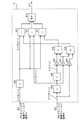
図1は、本発明の第1の実施の形態に係る画像変換装置100を示すブロック図である。図1に示す画像変換装置100は、第1の1フィールド遅延回路1、第2の1フィールド遅延回路2、第3の1フィールド遅延回路3、第1のプログレッシブ映像生成回路4、第2のプログレッシブ映像生成回路5、比較回路6、フレーム間補間回路7、フィールド内補間回路8および出力回路9を備える。また、図示していないが、画像変換装置100は、インタレース映像信号V1の同期信号、またはそれに対応する信号を受けてこれらの各ブロックに必要なタイミング信号を発生するタイミング発生回路を備えている。
【0087】
画像変換装置100の動作について以下に説明する。まず、インタレース映像信号V1は、連続して接続された第1の1フィールド遅延回路1、第2の1フィールド遅延回路2および第3の1フィールド遅延回路3により順々に遅延される。それにより、1フィールド遅れのインタレース映像信号a、2フィールド遅れのインタレース映像信号bおよび3フィールド遅れのインタレース映像信号cがそれぞれ生成される。したがって、1フィールドずつ連続して遅延した4つのインタレース映像信号が生成されることになる。
【0088】
これらの4つのインタレース映像信号のそれぞれは、第1のオッドフィールド信号、第1のイーブンフィールド信号、第2のオッドフィールド信号および第2のイーブンフィールド信号によって構成されるか、または、第1のイーブンフィールド信号、第1のオッドフィールド信号、第2のイーブンフィールド信号および第2のオッドフィールド信号によって構成されることになる。なお、インタレース映像信号は2フィールドで画面の全走査線を構成するので、ここではその一方のフィールドをオッドフィールドと呼び、他方をイーブンフィールドと呼んでいる。
【0089】
第1のプログレッシブ映像生成回路4にはインタレース映像信号a,b,cが与えられる。第1のプログレッシブ映像生成回路4はそれらの信号からプログレッシブ映像フィールド信号P1を生成し、比較回路6に与える。また、第2のプログレッシブ映像生成回路5にはインタレース映像信号V1,a,bが与えられる。第2のプログレッシブ映像生成回路5はそれらの信号からプログレッシブ映像フィールド信号P2を生成し、比較回路6に与える。
【0090】
比較回路6は、プログレッシブ映像フィールド信号P1とプログレッシブ映像フィールド信号P2とを比較して動き量情報Mを演算し、出力回路9に与える。
【0091】
また、インタレース映像信号V1およびインタレース映像信号bはフレーム間補間回路7に与えられる。フレーム間補間回路7は、時間的に2フィールド前後のフィールド間で補間処理するフレーム間補間によってフレーム間補間信号F1を生成し、出力回路9に与える。
【0092】
また、インタレース映像信号aはフィールド内補間回路8に与えられる。フィールド内補間回路8は、インタレース映像信号aからフィールド内補間によってフィールド内補間信号F2を生成し、出力回路9に与える。
【0093】
出力回路9は、動き量情報Mに応じてフレーム間補間信号F1およびフィールド内補間信号F2を画素ごとに割合を変えて生成したプログレッシブ映像信号V2を出力する。動き量情報Mが小さい場合には静止画の確率が高くなるので、出力回路9は、フレーム間補間信号F1の割合が多くなるようにプログレッシブ映像信号V2を生成する。
【0094】
本実施の形態に係る画像変換装置100は、1フィールドずつ連続して遅延した4つのインタレース映像信号のうち1〜3番目のインタレース映像信号からプログレッシブ映像フィールド信号P2を生成し、2〜4番目のインタレース映像信号からプログレッシブ映像フィールド信号P1を生成する。
【0095】
次に、画像変換装置100は、このプログレッシブ映像フィールド信号P1とプログレッシブ映像フィールド信号P2とを比較し、その比較結果を動き量情報Mとして出力することができる。それにより、画像変換装置100は、正確な動き判定を行うことができる。したがって、垂直方向の大きな輝度差を持つ画像がゆっくり動いたときなどにおいても、正確な動き判定をすることができ、安定で解像度の高いプログレッシブ映像信号を提供することができる。
【0096】
以下、本発明の効果を、従来例で画質劣化が生じた図16に示す垂直方向に正弦波的に輝度が変化する画像が図18に示すように垂直方向にゆっくり動いたときの動作の例を用いて説明する。
【0097】
元となる映像信号の値とインタレース映像信号としてサンプリングされた後の映像信号の値とは表5(a)および表5(b)に従来例の表1(a)および表1(b)と同様に示される。表5(a)および表5(b)は、f1フィールドからf9フィールドまでの9フィールド分を示している。
【0098】
【表5】
表5(a)には元となる映像信号の各フィールドの各ラインの値が示され、表5(b)にはインタレース映像信号としてサンプリングされた後の信号の各フィールドの各ラインの値が示されている。一般的に表5(b)に示すインタレース映像信号がフィールドごとに順番に伝送されている。図1においても表5(b)に示されるインタレース映像信号が、フィールド毎に順番に画像変換装置100にインタレース映像信号V1として与えられる。
【0100】
インタレース映像信号V1は、第1の1フィールド遅延回路1、第2の1フィールド遅延回路2および第3の1フィールド遅延回路3に与えられる。第1のプログレッシブ映像生成回路4および第2のプログレッシブ映像生成回路5はそれぞれが補間処理によりプログレッシブ映像フィールド信号P1およびプログレッシブ映像フィールド信号P2を生成する。その動作を以下に詳しく説明する。
【0101】
図2(a)は、第2のプログレッシブ映像生成回路5の内部の構成例を示し、図2(b)は、第1のプログレッシブ映像生成回路4の内部の構成例を示す。
【0102】
図2(a)の入力端子501には図1のインタレース映像入力V1が与えられ、入力端子502にはインタレース映像信号aが与えられ、入力端子503にはインタレース映像信号bが与えられる。
【0103】
図2(b)の入力端子401には図1のインタレース映像信号aが与えられ、入力端子402にはインタレース映像信号bが与えられ、入力端子403にはインタレース映像信号cが与えられる。
【0104】
図2(a)の第2のプログレッシブ映像生成回路5は、1クロックの遅延回路504〜508、乗算回路509〜514、加算回路515および切り換え回路516を備える。
【0105】
図2(b)の第1のプログレッシブ映像生成回路4は、1クロックの遅延回路404〜408、乗算回路409〜414、加算回路415および切り換え回路416を備える。
【0106】
乗算回路409、411、412、414、509、511、512、514ではそれぞれ1/8の乗算が行われ、乗算回路410、413、510、513では1/4の乗算が行われる。
【0107】
加算回路415では乗算回路409〜414から出力された信号が加算される。同様に加算回路515では乗算回路509〜514から出力された信号が加算される。
【0108】
このような構成により、第1のプログレッシブ映像生成回路4では、インタレース映像信号a,cがそれぞれ水平方向にフィルタリングされた後に平均化され、加算回路415に与えられる。
【0109】
切り換え回路416は、タイミング発生回路(図示せず)から与えられる信号K1に基づいて、インタレース映像信号bが現ラインの信号であれば1クロック遅延回路406で1フィールド遅延されたインタレース映像信号bを出力し、インタレース映像信号bが補間ラインの信号であれば加算回路415で生成された信号を出力する。
【0110】
また、同様に第2のプログレッシブ映像生成回路5では、インタレース映像信号V1およびインタレース映像信号bがそれぞれ水平方向にフィルタリングされた後に平均化されて、加算回路515に与えられる。
【0111】
切り換え回路516は、タイミング発生回路(図示せず)から与えられる信号K2に基づいて、インタレース映像信号aが現ラインの信号であれば1クロック遅延回路506でインタレース映像信号aを1フィールド遅延した信号を出力し、インタレース映像信号aが補間ラインの信号であれば加算回路515で生成された信号を出力する。
【0112】
また、第1のプログレッシブ映像生成回路4、第2のプログレッシブ映像生成回路5の内部で行われているフィルタ処理(フィルタリング)および加算処理が、補間ラインに対する第1のフィールドおよび第3のフィールドの対応する画素とその周辺の画素の演算、または、第2のフィールドおよび第4のフィールドの対応する画素とその周辺の画素の演算に相当している。特にこの場合、平均値が算出されている。
【0113】
平均値を用いれば複雑な演算を簡略化することができ、回路の規模を削減することができるが、これに限らなくてもよい。例えば、フィールド間の重みの大小を考慮して、各フィールドの寄与する大きさを変えて補間処理を行うことも可能である。
【0114】
表6(a)および表6(b)は、このような動作によって、第1のプログレッシブ映像生成回路4および第2のプログレッシブ映像生成回路5から出力された信号をそれぞれ示す。
【0115】
【表6】
表6(a)および表6(b)において、ハッチングの部分が補間ラインとして演算によって求められた部分である。また、この演算の例については、水平方向に同じ値の信号が続いているとして、水平方向の影響はないものとしている。
【0117】
もちろん、実際の装置については水平方向のフィルタ演算を行うことによってノイズ等の影響を低減できる。
【0118】
表6(a)のf4フィールドのLラインの値は、以下のようにして算出される。例えば、インタレース映像信号V1としてf4フィールドの信号が画像変換装置100に与えられた場合を説明する。表5(b)に示すように、f4フィールドのLラインは信号が伝送されていないので、補間処理を行う必要がある。インタレース映像信号V1としてf4フィールドの信号が入力されたときには、第3の1フィールド遅延回路3からはf1フィールドの信号が出力され、第2の1フィールド遅延回路2からはf2フィールドの信号が出力され、第1の1フィールド遅延回路1からはf3フィールドの信号が出力される。
【0119】
このとき、プログレッシブ映像フィールド信号P1の補間ラインは、第3の1フィールド遅延回路3から出力されるf1フィールドと第1の1フィールド遅延回路1のf3フィールドのそれぞれの現ラインの値から演算される。この場合は平均値(または平均値に近い値)が演算される。
【0120】
したがって、表5(a)より、f4フィールドのLラインの値は、f1フィールドのLラインの値「218」とf3フィールドのLラインの値「37」の平均値「(218+37)/2=127.5」を近傍の整数値として四捨五入により求めた値「128」となる。同様にして、それぞれの補間ラインの信号が求められる。なお、表6(a)において「−」と記された欄は表5(b)だけでは値が求まらないので表示を省略している。
【0121】
また、表6(b)のf3フィールドのLラインの値は、以下のようにして算出される。インタレース映像信号V1としてf3フィールドが画像変換装置100に与えられた場合には、第2の1フィールド遅延回路2からはf1フィールドが出力され、第1の1フィールド遅延回路1からはf2フィールドが出力される。
【0122】
このとき、プログレッシブ映像フィールド信号P2の補間ラインは、第2の1フィールド遅延回路2の出力のf1フィールドの現ラインの値とインタレース映像信号V1の信号であるf3フィールドの現ラインの値とから演算される。この場合は平均値(または平均値に近い値)が演算される。したがって、f4フィールドのLラインの値は、表5(a)に示すf1フィールドのLラインの値「218」とf3フィールドのLラインの値「37」の平均値「(218+37)/2=127.5」を近傍の整数値として四捨五入により求めた値「128」となる。同様にして、それぞれの補間ラインの信号が求められる。
【0123】
次に、比較回路6の動作について詳しく説明する。図3は、比較回路6の内部の構成例を示す。
【0124】
図3に示すように、入力端子601にはプログレッシブ映像フィールド信号P2が与えられ、入力端子602にはプログレッシブ映像フィールド信号P1が与えられる。
【0125】
比較回路6は、1ライン遅延回路603〜605、乗算回路606〜608、加算回路609,610、減算回路611〜613および最小値選択回路614を備える。
【0126】
入力端子601に与えられたプログレッシブ映像フィールド信号P2は1ライン遅延回路603に与えられる。入力端子602に与えられたプログレッシブ映像フィールド信号P1は1ライン遅延回路604に与えられる。この1ライン遅延回路604から出力される信号は1ライン遅延回路605に与えられる。
【0127】
乗算回路606は1ライン遅延回路605から出力された信号を1/2倍し、乗算回路607は1ライン遅延回路604から出力された信号を1/2倍し、乗算回路608はプログレッシブ映像フィールド信号P1を1/2倍する。
【0128】
加算回路609は乗算回路606,607から出力された信号を加算し、加算回路610は乗算回路607,608から出力された信号を加算する。
【0129】
減算回路611は、1ライン遅延回路603から出力された信号と加算回路609から出力された信号とを減算した値を求め、その値の絶対値を出力する。減算回路612は、1ライン遅延回路603から出力された信号と1ライン遅延回路604から出力された信号とを減算した値を求め、その値の絶対値を出力する。減算回路613は、1ライン遅延回路603から出力された信号と加算回路610から出力された信号とを減算した値を求め、その値の絶対値を出力する。
【0130】
最小値選択回路614は、減算回路611〜613から出力された信号の最小値を選択する。最小値選択回路614から出力された信号は、比較回路6からの出力信号として出力端子615から出力される。
【0131】
この動作は、入力端子601に第2のプログレッシブ映像生成回路5が生成する補間ラインが与えられたときに、その補間ラインの画素と入力端子602に与えられたプログレッシブ映像フィールド信号P1の対応する画素との間で行われる。すなわち、この動作は、プログレッシブ映像フィールド信号P1およびプログレッシブ映像フィールド信号P2の対応する画素間の比較と対応する画素およびその周辺の画素の値の画素ごとの比較とにより、その結果を動き量情報Mとして出力することに相当している。
【0132】
この比較演算の結果を表7(a)に示す。なお表7において、縦のラインの欄および横のフィールドの欄は第1の1フィールド遅延回路1から出力されるインタレース映像信号aのタイミングである。
【0133】
【表7】
例えば、f4フィールドのL+2ラインが比較回路6に与えられる場合の演算は下記のようになる。この場合の減算回路611には、プログレッシブ映像フィールド信号P2のf4フィールドのL+1ラインの値である値「191」が入力される。
【0135】
また、プログレッシブ映像フィールド信号P1のf4フィールドのLラインの値「128」とL+1ラインの値「255」との平均値「191.5」が乗算回路607,608および加算回路610から求められ、その近傍の整数値「191」が減算回路611に与えられる。したがって、減算回路611は、減算値の絶対値「0」を出力する。
【0136】
また、減算回路612には、プログレッシブ映像フィールド信号P2のf4フィールドのL+1ラインの値「191」とプログレッシブ映像フィールド信号P1のf4フィールドのL+1ラインの値「255」とが与えられる。したがって、減算回路612は、減算値の絶対値「64」を出力する。
【0137】
また、減算回路613には、プログレッシブ映像フィールド信号P2のf4フィールドのL+1ラインの値「191」が与えられる。また、減算回路613には、プログレッシブ映像フィールド信号P1のf4フィールドのL+1ラインの値「255」とL+2の値である値「128」との平均値「191」が与えられる。したがって、減算回路613は、減算値の絶対値「0」を出力する。
【0138】
この3つの演算結果が表7(a)のf4フィールドのL+1ラインの欄に値「0」、「64」および「0」として記載されている。同様にして表7(a)のハッチングのある補間ラインの欄には、減算回路611〜613からの演算結果の値が表示されている。
【0139】
表7(b)は、この減算回路611〜613与えられる値の最小値を示している。例えば、f4フィールドのL+1ラインでは、減算回路611〜613からの出力信号である値「0」、「64」および「0」のなかの最小値である値「0」が選択されて表示されている。
【0140】
このように、比較回路6の動作として上述したような演算の例を示したが、比較回路6の演算は上記に限定されるものではない。例えば、さらに周辺のラインの値を加味して演算してもよい。その場合、さらに周辺の画素との演算が可能となるので、より精度の高い比較が可能となり、またノイズ等にも強い構成とすることができる。
【0141】
また、本実施の形態に係る画像変換装置100は、プログレッシブ映像フィールド信号P2の補間ラインの画素について、プログレッシブ映像フィールド信号P1の現ラインの対応する画素の信号の値と現ラインの画素の上下の補間ラインの画素の値との差を演算することによって動き量情報Mを求めている。しかしながら、これとは反対に、プログレッシブ映像フィールド信号P1の補間ラインの画素について、プログレッシブ映像フィールド信号P2の現ラインの対応する画素の信号の値と現ラインの画素の上下の補間ラインの画素の値との差を演算することによって動き量情報Mを求めてもよく、また、この両者を組み合わせる構成としてもよい。
【0142】
次に、フレーム間補間回路7およびフィールド内補間回路8の動作について詳しく説明する。
【0143】
図4は、フレーム間補間回路7の内部の構成例を示し、図5は、フィールド内補間回路8の構成例を示す。
【0144】
図4に示すように、フレーム間補間回路7は1/2乗算回路703,704、加算回路705を備える。フレーム間補間回路7の入力端子701には、図1のインタレース映像入力信号V1が与えられる。入力端子702には、インタレース映像信号bが与えられる。
【0145】
フレーム間補間回路7に与えられたインタレース映像信号V1,bは、それぞれ乗算回路703、704でそれぞれ1/2に乗算された後に加算回路705で加算され、フレーム間補間信号F1として出力706より出力される。
【0146】
また、フレーム間補間回路7は、図示していないタイミング発生回路からの信号によりタイミング制御され、注目するフィールドの補間ラインの演算を行うように動作する。
【0147】
図5に示すように、フィールド内補間回路8は、1ライン遅延回路802、1/2乗算回路803,804および加算回路805を備える。
【0148】
フィールド内補間回路8の入力端子801には、図1のインタレース映像信号aが与えられる。インタレース映像信号aは、1ライン遅延回路802および乗算回路804に与えられる。乗算回路803は、与えられた信号に1/2を乗算した後、加算回路805に与える。乗算回路804は、与えられた信号に1/2を乗算した後に加算回路805に与える。
【0149】
加算回路805は与えられた信号を加算し、出力端子806からフレーム間補間信号F2として出力する。
【0150】
また、フレーム間補間回路7と同様に、フィールド内補間回路8は、図示していないタイミング発生回路からの信号でタイミング制御され、注目するフィールドの補間ラインの演算を行うように動作する。
【0151】
フレーム間補間回路7およびフィールド内補間回路8の出力信号の一例を、それぞれ下記に示す。
【0152】
【表8】
表8(a)は、フレーム間補間回路7から出力された信号を示し、表8(b)は、フィールド内補間回路8から出力された信号を示す。この表においてハッチングがある部分が、注目フィールドの補間ラインの信号であり、これらの値が演算される。なお、表8は、インタレース映像信号aのタイミングにおける補間処理の値を表示している。
【0154】
例えば、表8(a)においてf3フィールドのLラインの欄の値は以下の通りとなる。つまり、インタレース映像信号aがf3フィールドのLラインの場合の値を下記の通りに求められる。
【0155】
この場合、フレーム間補間回路7の入力端子701にはインタレース映像信号V1のf3フィールドのLラインの値「37」(表5(b)参照)が与えられる。また、フレーム間補間回路7の入力端子702にはインタレース映像信号bのf1フィールドのLラインの値「218」が与えられる。フレーム間補間回路7は、与えられた値を乗算回路703,704のそれぞれで1/2に乗算し、加算回路705においてそれぞれの値を加算した値「127.5」の近傍の整数値「128」を求める。同様にして、その他のハッチングされた部分の値も演算される。
【0156】
次に、フィールド内補間回路8から出力されるフィールド内補間信号F2の一例については表8(b)に示す。表8(b)も、インタレース映像信号aのタイミングにおける補間処理の値を示している。一例として、インタレース映像信号aがf3フィールドのL+1ラインにおける補間処理した値について以下に説明する。
【0157】
f3フィールドのL+1ラインがインタレース映像信号aである場合には、フィールド内補間回路8には第1の1フィールド遅延回路1からの出力であるf2フィールドのL+3ラインの値が入力される。このとき1ライン遅延回路802からは1ライン以上前の値、すなわちf2フィールドのL+1ラインの値「255」が出力されて乗算回路803で1/2に乗算される。また乗算回路804ではf2フィールドのL+3ラインの値である「0」が1/2に乗算されて出力されている。
【0158】
フィールド内補間回路8は、乗算回路803,804から与えられた信号を加算回路805で加算し、その値「127.5」の近傍値である「128」をフィールド内補間した値として求める。同様にして、その他のハッチングされた部分の数値が演算される。
【0159】
次に、出力回路9の動作について詳しく説明する。図6は、出力回路9の内部の構成例を示す。
【0160】
図6に示すように、出力回路9は、割合演算回路905、乗算回路906,907、加算回路908および切り換え回路909を備える。ここで、αは割合演算回路905により演算される割合値であり、0以上1以下の数値である。乗算回路907はα倍の乗算回路であり、乗算回路906は(1−α)倍の乗算回路である。
【0161】
入力端子901にはフレーム間補間信号F1が与えられ、入力端子902にはフィールド内補間信号F2が与えられる。また、入力端子904にはインタレース映像信号aが与えられ、入力端子903には動き量情報Mに応じた値が与えられる。
【0162】
割合演算回路905は、入力端子903から与えられる動き量情報Mに応じて出力回路9から出力する静止画と動画の割合を演算する割合演算回路である。
【0163】
割合演算回路905は、入力端子903から与えられた動き量情報Mにより、フレーム間補間信号F1とフィールド内補間信号F2との割合を決める係数である割合値αを特定する。例えば、比較回路6から出力される動き量情報Mについて、0≦M<10のときは「α=0」とし、10≦M<20のときは「α=0.2」とし、20≦M<30のときは「α=0.5」とし、30≦Mのときは「α=1」とするように決める。このように、出力回路9は、動き量情報Mが小さいほど割合値αが小さくなるように制御する。
【0164】
乗算回路906,907は、入力端子901,902からそれぞれ入力されたフレーム間補間回路7から出力された信号、フィールド内補間回路8からの出力信号をそれぞれ乗算し、加算回路908で加算する。
【0165】
このようにすれば、動き量情報Mが小さいほどフレーム間補間回路7の出力の割合が高くなるように制御することができる。
【0166】
切り換え回路909は、入力端子904に与えられたインタレース映像信号aと加算回路908から与えられた信号とを切り換える。切り換え回路909は、図示していないタイミング発生回路によって、注目するフィールドの信号が現ラインであればインタレース映像信号aを出力し、補間ラインであれば加算回路908から出力される信号を出力するように切り換えることができる。
【0167】
切り換え回路9の入力端子903には、表7(b)に示されている動き量情報Mが入力される。例えば、f4フィールド、f5フィールドおよびf8フィールドの動き量情報Mは「0」であるので、割合演算回路905から出力される割合値αは「0」と演算される。
【0168】
f6フィールド、f7フィールドおよびf9フィールドの動き量情報Mは「19」または「13」であるので、割合演算回路905から出力される割合値αは「0.2」と演算される。この割合値αは表7(b)のカッコ内に示されている。
【0169】
このように、出力回路9が割合値αの大小によって演算動作を行った結果を表9に示す。
【0170】
【表9】
表9(a)において、例えば、f4フィールドのL+1ラインの値は、動き量情報Mから求められる割合値αが値「0.0」(表7(b)参照)であるので、フレーム間補間回路7の出力値は値「191」(表8(a)参照)となる。また、例えばf6フィールドのL+1ラインの値は、動き量情報Mから求められる割合値αが値「0.2」(表7(b)参照)であるので、フレーム間補間回路7の出力値は「64」(表8(a)参照)に「0.8」(=1−0.2)を乗じた値「51.2」と、フィールド内補間回路8の出力値である値「128」(表8(b)参照)に値「0.2」を乗じた値「25.6」とを加えた値「76.8」の近傍値である値「77」となる。
【0172】
このように、ハッチングされている補間ラインの値と、ハッチングのない現ラインの値が表9(a)に示すように演算される。
【0173】
表9(b)に、表9(a)に示される出力回路9から出力される値と元の映像信号との差の絶対値を示したものを示す。表9(b)は、画像変換装置100での遅延分である1フィールドの時間差を加味して、以下のように差が計算されている。
【0174】
例えば、元の映像信号ではf5フィールドの+3ラインの値「218」はインタレース映像信号では伝送されないラインであるが、1フィールド分の遅延を加味して、出力回路9からは、f6フィールドのL+3ラインの値として値「179」が出力されている。このf5フィールドのL+3ラインの値「218」と出力されているf6フィールドのL+3ラインの値「179」との差の絶対値として値「39」が計算される。このようにして、補間ラインでの元の映像信号の値と出力回路9から出力された値との差が、表9(b)のように計算される。
【0175】
表9(b)に示されるように、本発明の第1の実施の形態に係る画像変換装置100によれば、補間ラインでの現信号との明るさの差を、値「40」以下に抑えることができる。この値は、表4(b)に示される従来例の補間ラインでの現信号との差である値「90」に比べて、大幅に小さくすることが実現できている。
【0176】
つまり、本実施の形態によれば画像がゆっくりと垂直方向に動いたときに動画処理となりやすく、画質が劣化しやすいという従来例での課題を大幅に軽減することが可能となっている。
【0177】
このように本実施の形態による画像変換装置100は、基になるフィールドが異なるプログレッシブ映像フィールド信号P1とプログレッシブ映像フィールド信号P2とを比較し、その比較結果を動き量情報Mとして出力することができるので、正確な動き検出を行うことができる。また、画像変換装置100は、垂直方向の大きな輝度差を持つ画像がゆっくり動いたときなどにおいても、正確な動き判定をすることができ、安定で解像度の高い映像を提供することができる。
【0178】
また、本実施の形態では、1フィールドずつ連続して遅延した4つのインタレース映像信号V1,a,b,cのうちインタレース映像信号V1,a,bからプログレッシブ映像フィールド信号P2を生成し、インタレース映像信号a,b,cからプログレッシブ映像フィールド信号P1を生成する。このプログレッシブ映像フィールド信号P1とプログレッシブ映像フィールド信号P2とを比較している。
【0179】
なお、プログレッシブ映像フィールド信号P1およびプログレッシブ映像フィールド信号P2の生成は、1フィールドずつ連続して遅延した4つのインタレース映像信号のフィールド信号で作成することに限定されない。例えば、インタレース映像信号V1,a,bのうちのインタレース映像信号V1のフィールド信号とインタレース映像信号aのフィールド信号とでプログレッシブ映像フィールド信号P1を作成し、インタレース映像信号a,bでプログレッシブ映像フィールド信号P2を作成してもよい。このようにすれば、フィールドメモリに蓄えるデータ量を削減することができ低コストで高性能の画像変換装置を提供することができる。
【0180】
また、本実施の形態においては、プログレッシブ映像フィールド信号P1の現ラインとして、インタレース映像信号aを用い、補間ラインとしてインタレース映像信号V1とインタレース映像信号bとの演算値を用い、プログレッシブ映像フィールド信号P2の現ラインとして、インタレース映像信号bのフィールド信号を用い、補間ラインとしてインタレース映像V1のフィールド信号とインタレース映像信号cのフィールド信号との演算値を用いている。
【0181】
これによって、多少の動きがあったとしても、補間ラインには、インタレース映像信号V1,bの演算により、また、インタレース映像信号a,bの演算により、相対的な動き量がキャンセルし合うように働くため、映像に動きがあったとしても、「静止画」、「動画」の判定を正確に行うことができ、高精度に画質を改善でき、より高画質なプログレッシブ映像を提供することができる。
【0182】
さらに補間ラインの信号を演算する上で、対応するインタレース映像信号の対応する画素とその周辺の画素を演算に含めている。これにより、ノイズに強く、より精度の高いプログレッシブ映像フィールド信号P1とプログレッシブ映像フィールド信号P2を生成することができ、より高精度の動き検出を行うことができる。
【0183】
さらに、補間ラインの信号を演算する上で、対応するインタレース映像フィールドの対応する画素の平均値を演算している。これにより、回路規模を簡略化することが可能となり、低コストな回路を実現できる。
【0184】
また、比較回路6は、第1のプログレッシブ映像生成回路4が生成したプログレッシブ映像フィールド信号P1と第2のプログレッシブ映像生成回路5が生成したプログレッシブ映像フィールド信号P2との対応する画素間の比較と対応する画素およびその周辺の画素の値を画素ごとの比較により、その結果を動き量Mとして出力するものである。
【0185】
この場合、比較回路6の比較が対応する画素だけにとどまらず、周辺の画素をも含むので、動き検出をより高精度で行うことができるものである。
【0186】
一般には、インタレース映像信号をインタレース映像フィールド信号と呼び、プログレッシブ映像信号を、特に、プログレッシブ画像フレーム信号と呼ぶことがある。
【0187】
本発明の実施の形態の説明においては、最終的な出力に至る前の中間的なプログレッシブ映像信号をテレビ映像のフィールド単位の処理信号であることから、プログレッシブ映像フィールド信号と記している。この名称について、特にフィールド信号は、合成されたフレーム信号と呼び変えても意味的には同じである。つまり、本発明においては、プログレッシブ映像フィールド信号をプログレッシブ画像フレーム信号と呼び変えても同じ意味を指すものであり、本発明は、プログレッシブ映像フィールド信号という表記に限定されない。すなわち、プログレッシブ映像フィールド信号は、インタレース映像フィールド信号から生成されたプログレッシブ映像信号を示すものである。
【0188】
本実施の形態においては、第1の1フィールド遅延回路1、第2の1フィールド遅延回路2および第3の1フィールド遅延回路3、第1のプログレッシブ映像生成回路4および第2のプログレッシブ映像生成回路5がプログレッシブ信号生成回路に相当し、第1の1フィールド遅延回路1、第2の1フィールド遅延回路2および第3の1フィールド遅延回路3がインタレース生成回路に相当し、プログレッシブ映像フィールド信号P1が第1のプログレッシブ信号に相当し、第1のプログレッシブ映像生成回路4が第1のプログレッシブ回路に相当し、プログレッシブ映像フィールド信号P2が第2のプログレッシブ信号に相当し、第2のプログレッシブ映像生成回路5が第2のプログレッシブ回路に相当する。
【0189】
また、比較回路6が動き算出回路に相当し、フレーム間補間信号F1が静止画プログレッシブ信号に相当し、フレーム間補間回路7が静止画処理回路に相当し、フィールド内補間信号F2が動画プログレッシブ信号に相当し、フィールド内補間回路8が動画処理回路に相当し、インタレース映像信号V1,a,b,cがそれぞれ第1〜第4のインタレース映像信号に相当する。
【0190】
(第2の実施の形態)
次に、第2の実施の形態に係る画像変換装置について説明する。第2の実施の形態に係る画像変換装置においては、図1の第1のプログレッシブ映像生成回路4が形成したプログレッシブ映像フィールド信号P1および第2のプログレッシブ映像生成回路5が形成したプログレッシブ映像フィールド信号P2のライン間に新たに複数の仮想の画素を形成する。
【0191】
その結果、第2の実施の形態に係る画像変換装置においては、第1の実施の形態に係る画像変換装置100と比較して、画像が1ライン/フィールド以下でゆっくり動いた時でも、複数の仮想の画素に基づいて、より精密に動き情報を検出できるとともに、最適な静止画処理と動画処理との制御を実現できる。
【0192】
図7は、第2の実施の形態に係る画像変換装置のブロック図である。図7に示す第2の実施の形態に係る画像変換装置100aが、図1に示す第1の実施の形態に係る画像変換装置100と異なる点は以下の点である。
第2の実施の形態に係る画像変換装置100aは、第1の実施の形態に係る画像変換装置100の構成に、第1の映像信号形成回路10および第2の映像信号形成回路11をさらに含むものである。
【0193】
また、第2の実施の形態に係る画像変換装置100aは、第1の実施の形態に係る画像変換装置100の比較回路6の代わりに比較回路6aを含み、第1の実施の形態に係る画像変換装置100の出力回路9の代わりに出力回路9aを含む。
【0194】
第2の実施の形態に係る画像変換装置100aのその他の構成は、第1の実施の形態に係る画像変換装置100の構成と同様であるので、同一構成部分には同一符号を付すものとする。
【0195】
以下、第2の実施の形態に係る画像変換装置100aが第1の実施の形態に係る画像変換装置100の構成と異なる点について説明する。
【0196】
第2の実施の形態に係る画像変換装置100aの第1の映像信号形成回路10は、第1のプログレッシブ映像生成回路4が出力するプログレッシブ映像フィールド信号P1の画素間に新たに画素を形成する。また、第2の映像信号形成回路11は、第2のプログレッシブ映像生成回路5が出力するプログレッシブ映像フィールド信号P2の画素間に新たに画素を形成する。
【0197】
次に、比較回路6aは、第1の映像信号形成回路10が出力する新たに形成されたプログレッシブ映像フィールド信号P3と第2の映像信号形成回路11が出力する新たに形成されたプログレッシブ映像フィールド信号P4とをそれぞれ対応する画素間で画素の値を比較して、または対応する画素とその周辺の画素の値とを比較して、その比較結果を動き量情報Maとして出力する。
【0198】
以下に、第1の映像信号形成回路10および第2の映像信号形成回路11の構成について説明する。
【0199】
図8(a)は第1の映像信号形成回路10の構成を示す図であり、図8(b)は第2の映像信号形成回路11の構成を示す図である。
【0200】
図8(a)に示すように、第1の映像信号形成回路10は、1ライン遅延回路1002,1003、乗算回路1004,1005,・・・,1015および加算回路1016,1017,・・・,1021を含む。
【0201】
また、乗算回路1005,1008,1011,1014のそれぞれの乗算係数は、1/4に設定されている。乗算回路1006,1007,1012,1013のそれぞれの乗算係数は、2/4に設定されている。乗算回路1004,1009,1010,1015のそれぞれの乗算係数は、3/4に設定されている。
【0202】
図8(b)に示すように、第2の映像信号形成回路11は、1ライン遅延回路1102,1103、乗算回路1104,1105,・・・,1115および加算回路1116,1117,・・・,1121を含む。
【0203】
また、乗算回路1105,1108,1111,1114のそれぞれの乗算係数は、1/4に設定されている。乗算回路1106,1107,1112,1113のそれぞれの乗算係数は、2/4に設定されている。乗算回路1104,1109,1110,1115のそれぞれの乗算係数は、3/4に設定されている。
【0204】
次に、図8(a)を用いて第1の映像信号形成回路10の動作について説明する。
【0205】
第1のプログレッシブ映像生成回路4から出力されたプログレッシブ映像フィールド信号P1が、入力端子1001に与えられる。入力端子1001に与えられたプログレッシブ映像フィールド信号P1は、1ライン遅延回路1002に与えられる。
【0206】
1ライン遅延回路1002は、プログレッシブ映像フィールド信号P1を1ライン分遅延し、プログレッシブ映像フィールド信号P11を生成し、その生成したプログレッシブ映像フィールド信号P11を1ライン遅延回路1003に与える。1ライン遅延回路1003は与えられたプログレッシブ映像フィールド信号P11を1ライン分遅延し、プログレッシブ映像フィールド信号P12を生成する。
【0207】
入力端子1001に与えられたプログレッシブ映像フィールド信号P1は、乗算回路1011,1013,1015にそれぞれ与えられる。1ライン遅延回路1002により生成されたプログレッシブ映像フィールド信号P11は、乗算回路1005,1007,1009,1010,1012,1014にそれぞれ与えられる。1ライン遅延回路1003により生成されたプログレッシブ映像フィールド信号P12は、乗算回路1004,1006,1008にそれぞれ与えられる。
【0208】
次に、乗算回路1004において、与えられたプログレッシブ映像フィールド信号P12が、設定された乗算係数と乗算されて加算回路1016へ出力される。乗算回路1005において、与えられたプログレッシブ映像フィールド信号P11が、設定された乗算係数と乗算されて加算回路1016へ出力される。乗算回路1006において、与えられたプログレッシブ映像フィールド信号P12が、設定された乗算係数と乗算されて加算回路1017へ出力される。
【0209】
乗算回路1007において、与えられたプログレッシブ映像フィールド信号P11が、設定された乗算係数と乗算されて加算回路1017へ出力される。乗算回路1008において、与えられたプログレッシブ映像フィールド信号P12が、設定された乗算係数と乗算されて加算回路1018へ出力される。乗算回路1009において、与えられたプログレッシブ映像フィールド信号P11が、設定された乗算係数と乗算されて加算回路1018へ出力される。乗算回路1010において、与えられたプログレッシブ映像フィールド信号P11が、設定された乗算係数と乗算されて加算回路1019へ出力される。
【0210】
乗算回路1011において、与えられたプログレッシブ映像フィールド信号P1が、設定された乗算係数と乗算されて加算回路1019へ出力される。乗算回路1012において、与えられたプログレッシブ映像フィールド信号P11が、設定された乗算係数と乗算されて加算回路1020へ出力される。乗算回路1013において、与えられたプログレッシブ映像フィールド信号P1が、設定された乗算係数と乗算されて加算回路1020へ出力される。乗算回路1014において、与えられたプログレッシブ映像フィールド信号P11が、設定された乗算係数と乗算されて加算回路1021へ出力される。乗算回路1015において、与えられたプログレッシブ映像フィールド信号P1が、設定された乗算係数と乗算されて加算回路1021へ出力される。
【0211】
続いて、加算回路1016において、乗算回路1004と乗算回路1005との出力信号が加算され、出力端子1022からプログレッシブ映像フィールド信号が出力される。加算回路1017において、乗算回路1006と乗算回路1007との出力信号が加算され、出力端子1023からプログレッシブ映像フィールド信号が出力される。加算回路1018において、乗算回路1008と乗算回路1009との出力信号が加算され、出力端子1024からプログレッシブ映像フィールド信号が出力される。
【0212】
加算回路1019において、乗算回路1010と乗算回路1011との出力信号が加算され、出力端子1026からプログレッシブ映像フィールド信号が出力される。加算回路1020において、乗算回路1012と乗算回路1013との出力信号が加算され、出力端子1027からプログレッシブ映像フィールド信号が出力される。加算回路1021において、乗算回路1014と乗算回路1015との出力信号が加算され、出力端子1028からプログレッシブ映像フィールド信号が出力される。1ライン遅延回路1002のプログレッシブ映像フィールド信号P11が、出力端子1025から出力される。図8(a)に示す第1の映像信号形成回路10においては、出力端子1022,・・・,出力端子1028から出力されるプログレッシブ映像フィールド信号が出力端子1029から出力される。
【0213】
上記の第1の映像信号形成回路10の動作は、タイミング発生回路(図示せず)の信号に基づいて演算される。なお、タイミング発生回路の信号は、第1のプログレッシブ映像生成回路4により生成されるプログレッシブ映像フィールド信号P1の補間ラインが、1ライン遅延回路1002から出力されるタイミングで形成されている。
【0214】
このとき、出力端子1022には、注目すべき補間ラインの画素の1/4の値と、補間ラインの上の現ラインの画素の3/4の値とが加算され出力されている。したがって、注目すべき補間ラインの画素から補間ラインの上の現ラインの画素への1ラインの3/4の距離にある場所の画素を形成したことになる。
【0215】
同様に、出力端子1023には、注目すべき補間ラインの画素の2/4の値と、補間ラインの上の現ラインの画素の2/4の値とが加算され出力されている。したがって、注目すべき補間ラインの画素から補間ラインの上の現ラインの画素への1ラインの2/4の距離にある場所の画素を形成したことになる。
【0216】
また、出力端子1024には、注目すべき補間ラインの画素の3/4の値と、補間ラインの上の現ラインの画素の1/4の値とが加算され出力されている。したがって、注目すべき補間ラインの画素から補間ラインの上の現ラインの画素への1ラインの1/4の距離にある場所の画素を形成したことになる。
【0217】
また、出力端子1026には、注目すべき補間ラインの画素の3/4の値と、補間ラインの下の現ラインの画素の1/4の値とが加算され出力されている。したがって、注目すべき補間ラインの画素から補間ラインの下の現ラインの画素への1ラインの1/4の距離にある場所の画素を形成したことになる。
【0218】
また、出力端子1027には、注目すべき補間ラインの画素の2/4の値と、補間ラインの下の現ラインの画素の2/4の値とが加算され出力されている。したがって、注目すべき補間ラインの画素から補間ラインの下の現ラインの画素への1ラインの2/4の距離にある場所の画素を形成したことになる。
【0219】
また、出力端子1028には、注目すべき補間ラインの画素の1/4の値と、補間ラインの下の現ラインの画素の3/4の値とが加算され出力されている。したがって、注目すべき補間ラインの画素から補間ラインの下の現ラインの画素への1ラインの3/4の距離にある場所の画素を形成したことになる。
【0220】
上記第1の映像信号形成回路10の出力例および第2の映像信号形成回路11の出力例を表に示す。
【0221】
【表10】
表10(a)は第1の映像信号形成回路10の出力端子1029からの出力信号を示し、表10(b)は第2の映像信号形成回路11の出力端子1129からの出力信号を示す。
【0223】
例えば、表10(a)に示すように、第1の映像信号形成回路10がf4フィールドのL+2ラインとL+1ラインとの間のL+1.25ラインの画素を算出する場合、L+1ラインの画素の値である「255」を3/4倍した値である「191.25」と、L+2ラインの画素の値である「128」を1/4倍した値である「32」とを加算して、その合計値「223.25」を算出する。そして、第1の映像信号形成回路10は、算出した合計値「223.25」の近傍値として「223」を選択し、f4フィールドのL+1.25ラインの画素の値として出力する。
【0224】
また、表10(b)に示すように、第2の映像信号形成回路11がf5フィールドのL+4ラインとL+5ラインとの間のL+4.25ラインの画素を算出する場合、L+4ラインの画素の値である「37」を3/4倍した値である「27.75」と、L+5ラインの画素の値である「128」を1/4倍した値である「32」とを加算して、その合計値「59.75」を算出する。そして、第2の映像信号形成回路11は、算出した合計値「59.75」の近傍値として「60」を選択し、f5フィールドのL+4.25ラインの画素の値として出力する。このようにして、他のラインの画素の値も算出され出力される。
【0225】
第1の映像信号形成回路10および第2の映像信号形成回路11では、上記のような演算が行われ、プログレッシブ映像フィールド信号P1,P2に新たに形成された画素を追加したプログレッシブ映像フィールド信号P3,P4が比較回路6aに出力される。
【0226】
次に、比較回路6aの構成および動作について説明する。図9は、比較回路6aの内部構成を示すブロック図である。
【0227】
比較回路6aは、バッファ回路6003,6004、動き演算回路6005および最小値回路6006を含む。
【0228】
比較回路6aの入力端子6001には、第1の映像信号形成回路10からプログレッシブ映像フィールド信号P3が与えられ、入力端子6002には第2の映像信号形成回路11からプログレッシブ映像フィールド信号P4が与えられる。入力端子6001,6002から与えられたプログレッシブ映像フィールド信号P3,P4は、バッファ回路6003,6004にそれぞれ与えられる。バッファ回路6003,6004は、所定の間隔でプログレッシブ映像フィールド信号P3,P4を蓄積し、所定の間隔経過後に動き演算回路6005にプログレッシブ映像フィールド信号P7,P8を与える。動き演算回路6005は、バッファ回路6003,6004の両者から与えられたプログレッシブ映像フィールド信号P7,P8において、対応する画素間、または対応する画素とその周辺の画素の値を比較し、その比較結果を動き量M1として出力する。
【0229】
最小値回路6006は、動き演算回路6005から出力された動き量M1から最小値を選択して出力端子6007から動き量情報Maとして出力する。
【0230】
次に、動き演算回路6005の動作例について説明する。動き演算回路6005は、入力されるプログレッシブ映像フィールド信号に基づいて動き検出を行う。
【0231】
まず、動き演算回路6005では、バッファ回路6003,6004からそれぞれ新たに画素を形成されたプログレッシブ映像フィールド信号P7,P8が与えられる。
【0232】
動き演算回路6005において、動き検出は、プログレッシブ映像フィールド信号のf4フィールドのL+3ラインの1画素、そのL+3ラインの上3画素、およびそのL+3ラインの下3画素の合計7画素に基づいて以下のように行われる。
【0233】
f4フィールドのL+3ラインの値は、表10(a)に示すf4フィールドのL+2.25ラインからL+3.75ラインの値と、表10(b)に示すf4フィールドのL+2.25ラインからL+3.75ラインの値とのそれぞれの差の絶対値を加算することによって求められる。
【0234】
すなわち、f4フィールドのL+3ラインの値は、次式で表される。
【0235】
【数1】
上式の値は、画像が全く動かず静止している場合に最も小さな値を示す。例えば、f4フィールドのL+3ラインの値が小さな値を示す場合、画素周辺での画像の変化が生じていないと判定できるため、画像が静止画であると推定できる。
【0237】
また、f4フィールドのL+3ラインの1つ上の値は、表10(a)に示すf4フィールドのL+2ラインからL+3.50ラインの値と、表10(b)に示すf4フィールドのL+2.25ラインからL+3.75ラインの値とのそれぞれの差の絶対値を加算することによって求められる。
【0238】
以下、同一フィールドにおいて上下に隣接する2つのライン間の距離を1画素/フィールドと表現し、上記2つのライン間の距離の1/2を0.5画素フィールドと表現し、上記2つのライン間の距離の1/4を0.25画素フィールドと表現し、上記2つのライン間の距離の3/4を0.75画素フィールドと表現する。
【0239】
すなわち、f4フィールドのL+3ラインの1つ上の値は、次式で表される。
【0240】
【数2】
上式の値は、画像が下ライン方向に0.25画素/フィールド動いている場合に最も小さな値を示す。
【0242】
また、f4フィールドのL+3ラインの2つ上の値は、表10(a)に示すf4フィールドのL+1.75ラインからL+3.25ラインの値と、表10(b)に示すf4フィールドのL+2.25ラインからL+3.75ラインの値とのそれぞれの差の絶対値を加算することによって求められる。
【0243】
すなわち、f4フィールドのL+3ラインの2つ上の値は、次式で表される。
【0244】
【数3】
上式の値は、画像が下ライン方向に0.50画素/フィールド動いている場合に最も小さな値を示す。
【0246】
このように、f4フィールドのL+3ラインの値は55と算出され、f4フィールドのL+3ラインの1つ上の値は「38」と算出され、f4フィールドのL+3ラインの2つ上の値は「18」と算出される。同様に、f4フィールドのL+3ラインの3つ上の値は「22」と算出され、f4フィールドのL+3ラインの1つ下の値は「71」と算出され、f4フィールドのL+3ラインの2つ下の値は「84」と算出され、f4フィールドのL+3ラインの3つ下の値は「98」とそれぞれ算出される。
【0247】
これらのf4フィールドのL+3ラインの値、L+3ラインの1つ上の値、L+3ラインの2つ上の値、L+3ラインの3つ上の値、L+3ラインの1つ下の値、L+3ラインの2つ下の値、L+3ラインの3つ下の値は、それぞれ動きの量が下方向に0.75画素/フィールド、下方向に0.50画素/フィールド、下方向に0.25画素/フィールド、静止、上方向へ0.25画素/フィールド、上方向へ0.50画素/フィールド、上方向へ0.75画素/フィールドの場合に最小値を示す。
【0248】
以上のように、動き演算回路6005では、プログレッシブ映像フィールド信号P7,P8の相関性に基づいて動き量および動きの方向とその確からしさとが算出され、動き量M1として出力される。上記の動き演算回路6005の動き量M1の出力結果を表に示す。
【0249】
【表11】
例えば、表11(a)に示すように、f4フィールドのL+3ラインの欄の上3欄と下3欄との値の中で、上側に0.50画素/フィールドの動きを示す欄が最小値である「18」を示している。その結果、映像フィールド信号の動き量および動き方向が下方向に0.50画素/フィールドであり、その確からしさは、「18」であると判定できる。
【0251】
なお、第2の実施の形態に係る画像変換装置100aにおいては、動き演算回路6005の出力のうちの最小値に基づいて動き方向および動き量とその確からしさとを判定することとしたが、これに限定されず、所定の閾値を設定して7つの欄のうちの最小値が所定の閾値以下の場合に動き量が小さいと判定させてもよい。
【0252】
例えば、所定の閾値を「20」に設定した場合、表11(a)よりf4フィールドのL+3ラインの欄の2つ上の欄に「20」以下の欄が存在するので、プログレッシブ映像フィールド信号P7,P8の相関性に基づいて、下方向に0.5画素/フィールドの動き量および動き方向を有すると判定できる。その結果、出力回路9へ出力する情報を削減することができ、回路を簡略化することが可能となる。
【0253】
このように、動き演算回路6005は、0.25画素/フィールド、0.50画素/フィールドおよび0.75画素/フィールドの動き量と確からしさとを算出して、最小値回路6006に動き量M1として与える。
【0254】
最小値回路6006は、注目する補間ラインの画素での動き演算回路6005から与えられる動き量M1のうち最小値を示す値を選択して動き量情報Maを出力端子6007に出力する。
【0255】
例えば、表11(a)に示すf4フィールドのL+3ラインの補間ラインでは、下方向に0.5画素/フィールドの動きを示す2つ上の欄の「18」が選択される。すなわち、表11(b)に示すように、下方向に0.5画素/フィールドで、その確からしさは「18」であるという値が出力される。
【0256】
上述したように、選択された値が小さいほど注目すべき補間ラインでの画素における動きの方向および動き量の確率が高いといえる。
【0257】
表11(b)は、上記のような動き量の最小値について、補間ラインでの画素ごとに値を示したものであり、この値が比較回路6aから動き量情報Maとして出力される。
【0258】
このように、第2の実施の形態に係る画像変換装置100aでは、ライン間に新たに画素が形成され、より解像度の高いプログレッシブ映像フィールド信号P3とプログレッシブ映像フィールド信号P4が形成され、これらを基にして比較回路6aにより動き量情報Maが算出される。
【0259】
したがって、第2の実施の形態に係る画像変換装置100aでは、精度の高い動き検出が可能となり、後述する出力回路での動画/静止画の出力割合の制御を正確にすることができるとともに、画質劣化が少なく解像度の高いプログレッシブ映像フィールド信号を生成することが可能となる。
【0260】
また、第2の実施の形態に係る画像変換装置100aの比較回路6aでは、演算時に対応する画素間および対応する画素とその周辺の画素との値を比較し、その比較結果を動き量として出力している。この結果、周辺の画素も演算に使用することができるので、演算精度が向上するとともに、プログレッシブ映像フィールド信号の動き量の検出精度を向上することができる。
【0261】
また、演算時に使用する画素の間の関係は、上記実施例に限らず、対応する画素同士による演算のみを行ってもよく、または対応する画素とその周辺の画素との演算のみを行ってもよく、それらの両者の演算をあわせて行ってもよい。
また、第2の実施の形態に係る画像変換装置100aにおいては、プログレッシブ映像フィールド信号P3とプログレッシブ映像フィールド信号P4とが形成され、これらに基づいて、動き量を演算しているが、これに限定されず、他の比較の方法を用いてもよい。
【0262】
例えば、プログレッシブ映像フィールド信号P3については、新たに形成した画素を使用することなく、プログレッシブ映像フィールド信号P1として元々存在していた画素を使用するものとし、その元々存在していた画素と新たに形成したプログレッシブ映像フィールド信号P4とを比較するものとしてもよい。
【0263】
また、例えば、プログレッシブ映像フィールド信号P4については、新たに形成した画素を使用することなく、プログレッシブ映像フィールド信号P2として元々存在していた画素を使用するものとし、その元々存在していた画素と新たに形成したプログレッシブ映像フィールド信号P3とを比較するものとしてもよい。
【0264】
このような場合には、第1の映像信号形成回路10または第2の映像信号形成回路11のいずれか一方を削減することができるため、回路規模を削減することができるとともに回路コストの低減を図ることができる。
【0265】
この場合、比較回路6aは、プログレッシブ映像フィールド信号P2およびプログレッシブ映像フィールド信号P3、プログレッシブ映像フィールド信号P1およびプログレッシブ映像フィールド信号P4、またはプログレッシブ映像フィールド信号P3およびプログレッシブ映像フィールド信号P4の対応する画素間、および対応する画素とその周辺の画素との値を比較し、その比較結果を動き量として出力することによって、動き量情報Maを算出することができる。
【0266】
次に、出力回路9aの動作を説明する。図10は、出力回路9aの内部構成の一例を示す図である。
【0267】
第2の実施の形態に係る出力回路9aが、第1の実施の形態に係る出力回路9と異なる点は、割合演算回路905の代わりに割合演算回路9005を含む点である。その他の構成は図6に示す割合演算回路905と同様であるので、同一部分には同一符号を付し、以下に異なる部分についてのみ説明する。
【0268】
図10に示す割合演算回路9005の入力端子903には、比較回路6aからの動き量および動き方向とその確からしさを示す数値が与えられる。
【0269】
割合演算回路9005は、与えられた動き量および動き方向とその確からしさを示す数値が所定の値以下である場合に静止画の割合が大きいと判定する。この場合、割合演算回路9005は、静止画の割合が大きくなるように割合値αを小さくして出力する。
【0270】
例えば、割合演算回路9005は、動き量および動き方向とその確からしさを示す数値(以下、動き量を示す数値と略記する。)に基づいて割合値αを以下のように設定する。
【0271】
動き量を示す数値が「0.50」以下のとき、割合値αとして「0」を出力し、動き量を示す数値が「0.75」以下のとき、割合値αとして「0.2」を出力し、動き量を示す数値が「1.00」以下のとき、割合値αとして「0.5」を出力し、動き量を示す数値が「1.00」よりも大きいとき、割合値αとして「1.0」を出力する。
【0272】
また、さらに、動き量を示す数値が「20」以下の値を示す場合は、正確な動きの方向および動き量を抽出していると判定して上記各条件を使用し、動き量を示す数値が「20」よりも大きな値を示す場合は、動きの方向および動き量が不確定であるとして割合値αを「1.0」に固定して出力するようにしてもよい。
【0273】
したがって、表11(b)に示す値が、割合検出回路9005に与えられた場合、全ての動き量を示す数値が「0.5」以下となり、割合検出回路9005は、乗算回路906,907に割合値αとして「0」を出力する。
【0274】
また、第2の実施の形態に係る割合値αの設定方法については、映像フィールド信号の動き量が1.0ライン以下のときに静止画の割合が大きくなるように設定しているが、これに限定されず、例えば、動き量を示す数値が「0.75」以下のときに静止画の割合値αを大きくしてもよく、動き量を示す数値が「0.50」以下のときに静止画の割合値αを大きくしてもよい。
【0275】
この場合、より正確な映像フィールド信号の動きを求めることができるとともに厳密に静止画の状態を検出することができるので、動画/静止画の検出精度を向上することができる。
【0276】
上記の条件によって、動き量を示す数値が「0.50」以下であるときに割合値αを0と設定した場合の出力回路9aの出力値を表に示す。
【0277】
【表12】
また、表12(a)により動き方向および動き量が確定された部分について補間画素の値を演算し、その確定された部分の演算結果とインタレースされる前の信号との差を表12(b)に示す。
【0279】
表12(b)については、表9(b)における計算と同様に、この回路での遅延分である1フィールドの時間差を加味して計算している。この表12(b)を表9(b)と比較するとf6フィールドでの誤差が、「39」から「26」に減少していることがわかる。
【0280】
以上のように、第2の実施の形態に係る画像変換装置100aは、第1の実施の形態に係る画像変換装置100よりも高精度に動画または静止画を検出することができるため、より正確に画像を変換できることを示している。
【0281】
すなわち、第2の実施の形態に係る画像変換装置100aは、従来の動き適応型プログレッシブ変換装置が有する、画像がゆっくりとライン方向に動いたときに動画処理となりやすく、画質が劣化しやすいという課題に対して、第1の実施の形態に係る画像変換装置100よりもさらに有効に課題を解決しているといえる。
【0282】
画像変換装置100aでは、新たに仮想の画素を形成したプログレッシブ映像フィールド信号P3とプログレッシブ映像フィールド信号P4とを用いて、それぞれの対応する画素間、および対応する画素とその周辺の画素の値とを比較し、その比較結果を動き量として出力検出したことによって、より精度の高い動き検出が可能になり、画質劣化の少ない解像度の高いプログレッシブ映像フィールド信号を生成することが可能となった。
【0283】
また、新たに画素を形成する際において、第1の映像信号形成回路10または第2の映像信号形成回路11は、それぞれプログレッシブ映像フィールド信号P3,P4のライン間に新たに画素を形成しているので、インタレース映像信号V1をプログレッシブ映像フィールド信号に変換する際により厳しい変換精度を要求される垂直方向に対しての精度を上げることができ、水平方向への新たに画素を生成する回路を省略できるので、回路規模の増大を低く抑えることができ、低コストに高精度の画像変換装置を提供することが可能となっている。
【0284】
第2の発明の実施の形態の説明においては、第1の1フィールド遅延回路1、第2の1フィールド遅延回路2および第3の1フィールド遅延回路3、第1のプログレッシブ映像生成回路4、第2のプログレッシブ映像生成回路5、第1の映像信号形成回路10および第2の映像信号形成回路11がプログレッシブ信号生成回路に相当し、第1の1フィールド遅延回路1、第2の1フィールド遅延回路2および第3の1フィールド遅延回路3がインタレース生成回路に相当し、プログレッシブ映像フィールド信号P1が第1のプログレッシブ信号に相当し、第1のプログレッシブ映像生成回路4が第1のプログレッシブ回路に相当し、プログレッシブ映像フィールド信号P2が第2のプログレッシブ信号に相当し、第2のプログレッシブ映像生成回路5が第2のプログレッシブ回路に相当し、第1の映像信号形成回路10が第1の画素形成回路に相当し、第2の映像信号形成回路11が第2の画素形成回路に相当する。
【0285】
また、比較回路6aが動き算出回路に相当し、フレーム間補間信号F1が静止画プログレッシブ信号に相当し、フレーム間補間回路7が静止画処理回路に相当し、フィールド内補間信号F2が動画プログレッシブ信号に相当し、フィールド内補間回路8が動画処理回路に相当し、インタレース映像信号V1,a,b,cがそれぞれ第1〜第4のインタレース映像信号に相当する。
【0286】
(第3の実施の形態)
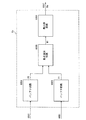
次に、第3の実施の形態に係る画像変換装置100bについて説明する。図11は、第3の実施の形態に係る画像変換装置の構成を示すブロック図である。
【0287】
図11に示す画像変換装置100bが、図1の第1の実施の形態に係る画像変換装置100の構成と異なる点は、フレーム間補間回路7が削除され、非適用領域検出回路12が付加され、出力回路9の代わりに出力回路9bを含む点である。その他の構成は図1の画像変換装置100bと同様であるので、同一部分には同一符号を付し、以下に異なる部分についてのみ説明する。
【0288】
図11の非適用領域検出回路12には、インタレース映像信号V1と第1の1フィールド遅延回路1からの出力信号であるインタレース映像信号aとが与えられる。
【0289】
非適用領域検出回路12は、インタレース映像信号V1およびインタレース映像信号aに基づいてそれぞれのフィールド間の画像に対応する画素を含む周辺画素の値の平均値を検出する。
【0290】
一般に、インタレース映像信号V1の平均値と、インタレース映像信号aとの平均値が大きく異なる場合、与えられた映像は、フィールド間で元々大きく信号値が変化するフリッカ性の画像であると考えられる。
【0291】
ここで、フリッカ性の画像とは、画像全体がちらつく状態、例えば、画像全体が1フィールド毎に白,黒,白,黒と繰り返し変化する状態をいう。実際には、暗室で連続してストロボ(フラッシュ)を発光させた場合の映像信号において、フリッカ性の画像が形成されることとなる。
【0292】
このようなフリッカ性の画像においては、静止画処理であるフレーム間の補間を行うと画質ひずみを生じるので、画像変換装置は、動画処理であるフィールド内補間処理の信号を出力すべきである。
【0293】
すなわち、白と黒とが交互に生じるフリッカ性の画像に対して静止画処理であるフレーム間の補間を行うと、白と黒との中間色であるグレーの画素の補間を行うこととなり、白のみの画像又は黒のみの画像において画質に歪が生じる。
【0294】
したがって、非適用領域検出回路12は、フリッカ性の画像であるか否かを検出して、動画処理であるフィールド内補間処理の信号を出力すべきか否かの旨を出力回路9bに与える。
【0295】
出力回路9bは、動画処理であるフィールド内補間処理の信号を出力すべき旨が非適用領域検出回路12から与えられたときに、フィールド内補間回路8の信号の割合を増加させて出力する。これによって、フリッカ性の画像、例えば連続したカメラのフラッシュ等が含まれる映像に対しても、誤って静止画処理をしないようにすることができ、より精度の高い画像変換装置100bを提供することができる。
【0296】
また、非適用領域検出回路12は、インタレース映像フィールドのフィールド間の映像信号の対応する画素を含む周辺の画素の信号の値の平均値を用いて検出している。その結果、比較的少ない回路規模で、より精度の高い画像変換装置100bを提供することが出来る。
【0297】
また、第3の実施の形態に係る画像変換装置100bでは、図1のフレーム間補間回路7が削除されて、フレーム間補間回路7からの出力の代わりに第2のプログレッシブ映像生成回路5の出力信号が出力回路9bに与えられている。これによって、フレーム間補間回路7が削減できるので、低コストの画像変換装置100bを提供することができる。
【0298】
(他の例)
次に、図11の非適用領域検出回路の他の例について説明する。図12は、非適用領域検出回路の他の例を示すブロック図である。
【0299】
図12に示す非適用領域検出回路12aは、第1の領域検出回路21、第2の領域回路22および判別回路30を含む。
【0300】
図12に示すようにインタレース映像信号V1が、第1の1フィールド遅延回路1および第1の領域検出回路21に与えられる。第1の1フィールド遅延回路1は、与えられたインタレース映像信号V1を1フィールド遅延させてインタレース映像信号aを生成し、そのインタレース映像信号aを第2の領域検出回路22に与える。
【0301】
第1の領域検出回路21は、与えられたインタレース映像信号V1から1ライン上における平均値AV1、1ライン上における最大値MAX1、1ライン上における最小値MIN1を判別回路30に与える。第2の領域検出回路22は、第1の1フィールド遅延回路1から与えられたインタレース映像信号aの1ラインの平均値AV2、1ラインの最大値MAX2、1ラインの最小値MIN2を判別回路30に与える。
【0302】
判別回路30は、第1の領域検出回路21および第2の領域検出回路22から与えられた平均値AV1,AV2、最大値MAX1,MAX2および最小値MIN1,MIN2に基づいて与えられた画像がフィールド間で元々大きく信号値が変化するフリッカ性の画像であるか否かを検出する。
【0303】
例えば、判別回路30は、第1の平均値AV1と第2の平均値AV2との差が第1の閥値より大きいか否かを判定する。次に、判別回路30は、第1の最大値MAX1と第1の最小値MIN1との差が第2の閥値より大きいか否かを判定する。さらに、判別回路30は、第2の最大値MAX2と第2の最小値MIN2との差が第3の閥値より大きいか否かを判定する。
【0304】
なお、フリッカ性の画像は、フィールド間で大きく信号値が変化するが、1フィールド内で大きく信号値が変化しない。
【0305】
そのため、判別回路30は、第1の平均値AV1と第2の平均値AV2との差が第1の閥値よりも大きく、第1の最大値MAX1と第1の最小値MIN1との差が第2の閥値よりも小さく、かつ第2の最大値MAX2と第2の最小値MIN2との差が第3の閥値よりも小さい場合に、フリッカ性の画像であると判定した非適用領域検出信号NIを出力回路9bに出力する。
【0306】
このように、非適用領域検出回路12aは、1ライン遅延させた映像信号の画素を含む周辺画素と、現ラインの画素を含む周辺画素との平均値を比較することにより、フリッカ性の画像であるか否かを正確に検出して、動画処理であるフィールド内補間処理の信号を出力すべきか否かの旨を出力回路9bに与えることができる。
【0307】
また、出力回路9bは、動画処理であるフィールド内補間処理の信号を出力すべき旨が非適用領域検出回路12aから与えられたときに、フィールド内補間回路8の信号の割合を増加させて出力する。これによって、フリッカ性の画像、例えば連続したカメラのフラッシュ等が含まれる映像に対しても、誤って静止画処理をしないようにすることができ、より精度の高い画像変換装置100bを提供することができる。
【0308】
また、非適用領域検出回路12aは、インタレース映像信号のフィールド間の画像の対応する画素を含む周辺の画素の信号の値の平均値によりフリッカ性の画像か否かを検出している。その結果、比較的少ない回路規模で、より精度の高い画像変換装置100bを提供することが出来る。
【0309】
(さらに他の例)
次に、図11の非適用領域検出回路のさらに他の例について説明する。図13は、非適用領域検出回路のさらに他の例を示すブロック図である。
【0310】
図13に示す非適用領域検出回路12bが、図12に示す非適用領域検出回路12aと異なる点は、非適用領域検出回路12aの構成にさらに第3の領域検出回路23および第2の1フィールド遅延回路2を含む点である。その他の構成は図12に示す非適用領域検出回路12aと同様であるので、同一部分には同一符号を付し、以下に異なる部分についてのみ説明する。
【0311】
図13に示すように、第1の1フィールド遅延回路1は、与えられたインタレース映像信号V1を1フィールド遅延させてインタレース映像信号aを生成し、そのインタレース映像信号aを第2の1フィールド遅延回路2および第2の領域検出回路22に与える。
【0312】
第2の1フィールド遅延回路2は、与えられたインタレース映像信号aを1フィールド遅延させてインタレース映像信号bを生成し、そのインタレース映像信号bを第3の領域検出回路23に与える。
【0313】
第3の領域検出回路23は、与えられたインタレース映像信号bから1ライン上における平均値AV3、1ライン上における最大値MAX3、1ライン上における最小値MIN3を判別回路30に与える。
【0314】
判別回路30は、第1の領域検出回路21、第2の領域検出回路22および第3の領域検出回路23から与えられた平均値AV1,AV2,AV3、最大値MAX1,MAX2,MAX3および最小値MIN1,MIN2,MIN3に基づいて与えられた画像がフィールド間で元々大きく信号値が変化するフリッカ性の画像であるか否かを検出する。
【0315】
そのため、例えば、判別回路30は、第1の平均値AV1と第2の平均値AV2との差が第1の閥値より大きいか否かを判定する。また、判別回路30は、第2の平均値AV2と第3の平均値AV3との差が第4の閥値より大きいか否かを判定する。
【0316】
次に、判別回路30は、第1の最大値MAX1と第1の最小値MIN1との差が第2の閥値より大きいか否かを判定する。判別回路30は、第2の最大値MAX2と第2の最小値MIN2との差が第3の閥値より大きいか否かを判定する。さらに判別回路30は、第3の最大値MAX2と第3の最小値MIN2との差が第5の閥値より大きいか否かを判定する。
【0317】
なお、フリッカ性の画像は、フィールド間で大きく信号値が変化するが、1フィールド内で大きく信号値が変化しない。
【0318】
判別回路30は、第1の平均値AV1と第2の平均値AV2との差が第1の閥値よりも大きく、第1の最大値MAX1と第1の最小値MIN1との差が第2の閥値よりも小さく、第2の最大値MAX2と第2の最小値MIN2との差が第3の閥値よりも小さく、第3の平均値AV3と第2の平均値AV2との差が第1の閥値よりも大きく、かつ第3の最大値MAX3と第3の最小値MIN3との差が第5の閥値よりも小さい場合に、フリッカ性の画像であると判定した非適用領域検出信号NIを出力回路9bに出力する。
【0319】
このように、非適用領域検出回路12aは、2ライン遅延させた映像信号の画素を含む周辺画素と、1ライン遅延させた映像信号の画素を含む周辺画素と、現ラインの画素を含む周辺画素との平均値を比較することにより、フリッカ性の画像であるか否かをより正確に検出して、動画処理であるフィールド内補間処理の信号を出力すべきか否かの旨を出力回路9bに与えることができる。
【0320】
また、出力回路9bは、動画処理であるフィールド内補間処理の信号を出力すべき旨が非適用領域検出回路12aから与えられたときに、フィールド内補間回路8の信号の割合を増加させて出力する。これによって、フリッカ性の画像、例えば連続したカメラのフラッシュ等が含まれる映像に対しても、誤って静止画処理をしないようにすることができ、特に精度の高い画像変換装置100bを提供することができる。
【0321】
第3の発明の実施の形態の説明においては、第1の1フィールド遅延回路1、第2の1フィールド遅延回路2および第3の1フィールド遅延回路3、第1のプログレッシブ映像生成回路4、第2のプログレッシブ映像生成回路5、第1の映像信号形成回路10および第2の映像信号形成回路11がプログレッシブ信号生成回路に相当し、第1の1フィールド遅延回路1、第2の1フィールド遅延回路2および第3の1フィールド遅延回路3がインタレース生成回路に相当し、プログレッシブ映像フィールド信号P1が第1のプログレッシブ信号に相当し、第1のプログレッシブ映像生成回路4が第1のプログレッシブ回路に相当し、プログレッシブ映像フィールド信号P2が第2のプログレッシブ信号に相当し、第2のプログレッシブ映像生成回路5が第2のプログレッシブ回路に相当し、第1の映像信号形成回路10が第1の画素形成回路に相当し、第2の映像信号形成回路11が第2の画素形成回路に相当し、非適用領域12,12a,12bが判定回路に相当する。
【0322】
また、比較回路6が動き算出回路に相当し、フレーム間補間信号F1が静止画プログレッシブ信号に相当し、フレーム間補間回路7が静止画処理回路に相当し、フィールド内補間信号F2が動画プログレッシブ信号に相当し、フィールド内補間回路8が動画処理回路に相当し、インタレース映像信号V1,a,b,cがそれぞれ第1〜第4のインタレース映像信号に相当する。
【0323】
【発明の効果】
本発明によれば、プログレッシブ信号に基づいて動き量が算出されるため、より正確で緻密な動き量を算出することができる。したがって、垂直方向の大きな輝度差を持つ画像が1ライン以下でゆっくり動いた場合でも正確な動き量を算出して画像の動きを判定することができるので、安定で解像度の高い映像を提供することができる。
【図面の簡単な説明】
【図1】本発明の第1の実施の形態に係る画像変換装置を示すブロック図
【図2】(a)は第1のプログレッシブ映像生成回路の内部の構成例を示す図、(b)は第2のプログレッシブ映像生成回路の内部の構成例を示す図
【図3】比較回路の内部の構成例を示す図
【図4】フレーム間補間回路の内部の構成例を示す図
【図5】フィールド内補間回路の構成例を示す図
【図6】出力回路の内部の構成例を示す図
【図7】第2の実施の形態に係る画像変換装置のブロック図
【図8】(a)は第1の映像信号形成回路の構成を示す図、(b)は第2の映像信号形成回路の構成を示す図
【図9】比較回路の内部構成を示すブロック図
【図10】出力回路の内部構成の一例を示す図
【図11】第3の実施の形態に係る画像変換装置の構成を示すブロック図
【図12】非適用領域検出回路の他の例を示すブロック図
【図13】非適用領域検出回路のさらに他の例を示すブロック図
【図14】インタレース映像信号の形態を示す図
【図15】従来の動き適応型プログレッシブ変換装置の構成を示すブロック図
【図16】垂直方向に正弦波的に輝度が変化する画像の一例を示す図
【図17】インタレース映像信号に変換される前の元となる映像信号を示す図
【図18】インタレース映像信号が1フィールドごとに1/2ラインずつ動いたときの映像信号を重ねた図
【符号の説明】
1 第1の1フィールド遅延回路
2 第2の1フィールド遅延回路
3 第3の1フィールド遅延回路
4 第1のプログレッシブ映像生成回路
5 第2のプログレッシブ映像生成回路
6,6a 比較回路
7 フレーム間補間回路
8 フィールド内補間回路
9,9a,9b 出力回路
10 第1の映像信号形成回路
11 第2の映像信号形成回路
23 第3の領域検出回路
30 判別回路
100,100a,100b 画像変換装置
V1,a,b,c インタレース映像信号
P1,P2,P3,P4 プログレッシブ映像フィールド信号
F1 フレーム間補間信号
F2 フィールド内補間信号[0001]
BACKGROUND OF THE INVENTION
The present invention relates to an image conversion apparatus and an image conversion method for converting an interlaced video signal into a progressive video signal.
[0002]
[Prior art]
Conventionally, a motion adaptive progressive converter has been used to convert an interlaced video signal into a progressive video signal (see, for example, Patent Document 1).
[0003]
FIG. 14 shows an example of an interlaced video signal. One frame of interlaced video signal is transmitted as a two-field image. For example, when L is an even value, signals of even lines such as L line, L + 2 line, L + 4 line, L + 6 line, and L + 8 line are transmitted in N field. Subsequently, in the N + 1 field, signals of odd-numbered lines such as L + 1 line, L + 3 line, L + 5 line, and L + 7 line are transmitted. In the next N + 2 field, the signal of the even-numbered line is transmitted as in the N field.
[0004]
Thus, the interlaced video signal is divided into two fields and transmitted, and one frame of video is displayed by the scanning lines of these two fields.
[0005]
The signal of the line which is not transmitted in each field is generated from the signals of the previous and subsequent fields or the current field (for example, the signals of the upper and lower lines). The signal and the transmitted signal are combined to form a progressive video signal.
[0006]
Hereinafter, a line actually transmitted in the current field is referred to as a current line, and a line generated from a plurality of temporally preceding and following fields or from a signal in the current field is referred to as an interpolation line.
[0007]
FIG. 15 shows a configuration example of a conventional motion adaptive progressive conversion apparatus. As shown in FIG. 15, the motion adaptive progressive conversion apparatus includes one-field delay circuits J1 and J2, a motion detection circuit J3, an inter-frame interpolation circuit J4, an intra-field interpolation circuit J5, and a switching circuit J6. The interlaced video signal J0 is delayed by one field by the one-field delay circuit J1 and the one-field delay circuit J2.
[0008]
The motion detection circuit J3 compares corresponding pixels on the same line between fields before or after two fields in time (hereinafter referred to as between frames). The motion detection circuit J3 determines that the pixels are “still images” when the difference between the compared pixel values is small, and determines the pixels as “moving image” when the difference between the compared pixel values is large. .
[0009]
The inter-frame interpolation circuit J4 generates a corresponding pixel from pixels on the same line between frames. For example, in FIG. 14, when interpolating the pixel X of the L + 4 line in the N + 1 field, the inter-frame interpolation circuit J4 uses, for example, “X” from the pixel A in the L + 4 line in the N field and the pixel B in the L + 4 line in the N + 2 field. = (A + B) / 2 "(A and B indicate the level of brightness of the pixel signal) to generate the pixel X.
[0010]
The intra-field interpolation circuit J5 generates a corresponding pixel from pixels on adjacent lines in the same field. For example, in FIG. 14, when interpolating the pixel X of the (L + 1) line in the (N + 1) field, the intra-field interpolation circuit J5 uses, for example, “X = (C + D) / 2 "(C and D indicate the brightness level of the signal of the pixel) to generate the pixel X.
[0011]
When the output of the one-field delay circuit J1 is the current line, the switching circuit J6 selects this current line signal and outputs it as the progressive video signal J7. When the motion detection circuit J3 determines that the target pixel is “still image”, the switching circuit J6 outputs a signal provided from the inter-frame interpolation circuit J4 as a progressive video signal J7, and the motion detection circuit J3 sets the target pixel as “moving image”. If it is determined, the generated signal supplied from the intra-field interpolation circuit J5 is output as the progressive video signal J7.
[0012]
In the case of an apparatus having such a configuration, a progressive video signal generated by inter-frame interpolation (interpolation performed from the previous or second field in time) is output for a still image having a large correlation between frames. The On the other hand, for a moving image with low correlation between frames, a progressive video signal generated by intra-field interpolation is output. Therefore, according to this method, in theory, it should be possible to perform an interpolation process that substantially matches the motion of the image.
[0013]
[Patent Document 1]
JP-A-10-112845
[0014]
[Problems to be solved by the invention]
However, the conventional method cannot accurately determine when an image with a large luminance difference in the vertical direction moves slowly, so inter-frame interpolation processing suitable for still images and intra-field interpolation processing suitable for movies May not be performed properly and the image may deteriorate.
[0015]
An example of such a case is shown below. FIG. 16 shows an original video signal before being converted into an interlaced video signal. The degree of brightness (luminance) of this video signal changes sinusoidally. The vertical axis represents luminance, and the horizontal axis represents line numbers. The brightness of black is displayed as the lowest value “0”, and the brightness of white is displayed as the maximum value “255”. The numerical values in the figure indicate sample values after sampling.
[0016]
The luminance of the original video signal is the value “218” for the L line, the maximum luminance of “255” between the L line and the L + 1 line, the value “218” for the L + 1 line, the L + 1 line and the L + 2 line. The value becomes “128” between the L + 2 line, the value “37” between the L + 2 line and the L + 3, the minimum luminance value “0” between the L + 2 line and the L + 3, the value “37” between the L + 3 line and the L + 3 line and the L + 4 line. The value becomes “128” in between, and the value “218” in the L + 4 line. Similarly, the line after the L + 5 line also changes. When this image is transmitted as an interlaced video signal, it is as shown in FIG. That is, a black circle value is transmitted in a certain field, and a white circle value is transmitted in the next field.
[0017]
FIG. 18 shows a superposition of such interlaced video signals when the interlaced video signals are moved by ½ line for each field. That is, in the f1 field, the value “218” is transmitted as the L line, the value “37” is transmitted as the L + 2 line, the value “218” is transmitted as the L + 4 line, and the value “37” is transmitted as the L + 6 line.
[0018]
Subsequently, since the waveform of the original video signal moves by 1/2 line in the f2 field, the value “255” as the L + 1 line, the value “0” as the L + 3 line, the value “255” as the L + 5 line, and the L + 7 line The value “0” is transmitted. Hereinafter, in the f3 field, f4 field, f5 field, and f6 field, the luminance value of the video signal is transmitted as shown in the figure. Table 1 shows the relationship between the line and the sample value in each field.
[0019]
[Table 1]
Table 1 (a) shows the luminance value of the original video signal before being sampled as an interlace video signal in each field, and Table 1 (b) shows the video signal after being sampled as an interlace video signal. The brightness value is shown. A line that is subjected to interpolation signal processing on the receiver side that has received the interlaced video signal and is not transmitted, that is, the luminance value in the “−” column of Table 1 (b), is obtained and converted to a progressive video signal.
[0021]
The operation when such an interlaced video signal is processed by the conventional motion adaptive progressive conversion apparatus shown in FIG. 15 will be described. In the conventional motion adaptive progressive conversion device, the motion detection circuit J3 has a luminance value difference between an interlaced video signal of a certain field and an interlaced video signal of a field that is two fields later or previous in time. It is determined whether the pixel of interest is a “still image” or a “moving image”. The determination result is sent to the switching circuit J6.
[0022]
If the determination result by the motion detection circuit J3 is “still image”, the switching circuit J6 outputs a signal supplied from the inter-frame interpolation circuit J4 as a progressive video signal J7. If the determination result by the motion detection circuit J3 is “moving image”, a signal given from the intra-field interpolation circuit J5 is output as a progressive video signal J7.
[0023]
First, the operation of the motion detection circuit J3 will be described with reference to Table 2 (a) and Table 2 (b).
[0024]
[Table 2]
Table 2 (a) shows the difference between the luminance value of the interlaced video signal of a certain field and the luminance value of the interlaced video signal of two fields after or before the field. The values in Table 2 (a) are calculated by the motion detection circuit J3. For example, the luminance value of the L line in the f2 field is the value “181” obtained by taking the difference between the L line value “218” in the f1 field and the L line value “37” in the f3 field. Similarly, the luminance value of each line in each field is calculated.
[0026]
Table 2 (b) shows the result of the motion detection circuit J3 determining whether the pixel of interest is a “moving image” or a “still image” based on the luminance values in Table 2 (a). Here, the threshold value of the brightness of the moving image and the still image is set to “20”. When the threshold is “20” or more, the motion detection circuit J3 determines the target pixel as “moving image”, and when it is “19” or less, the motion detection circuit J3 determines the target pixel as “still image”.
[0027]
Next, operations of the inter-frame interpolation circuit J4 and the intra-field interpolation circuit J5 will be described.
[0028]
[Table 3]
Table 3 (a) shows the output value of the inter-frame interpolation circuit J4. For example, in the L line of the f2 field of video input, the interlaced video signal is not actually transmitted but is obtained by interpolating signal processing between frames. Therefore, the luminance value of the L line of the f2 field in the inter-frame interpolation circuit J4 is averaged between the L line value “218” of the f1 field and the L line value “37” of the f3 field in Table 1 (b). That is, “(218 + 37) / 2 = 128” is calculated. The other luminance values in Table 3 (a) are similarly calculated as the average of the luminance values between frames.
[0030]
On the other hand, Table 3 (b) shows the output value of the intra-field interpolation circuit J5. For example, when performing the inter-field interpolation process on the luminance value of the L + 1 line of the f1 field, the average is obtained from the value “37” of the L + 2 line of the same f1 field as the value “218” of the L line of the f1 field in Table 1 (b). Is calculated and “(218 + 37) / 2 = 128” is calculated. The other luminance values in Table 3 (b) are similarly calculated as the average of the values of the upper and lower lines in the field.
[0031]
Next, the operation of the switching circuit J6 will be described. The switching circuit J6 is supplied with a signal given from the inter-frame interpolation circuit J4, a signal given from the intra-field interpolation circuit J5, a current line signal, and a signal given from the motion detection circuit J3.
[0032]
Table 4 below shows the luminance value of the progressive video signal J7 output from the switching circuit J6.
[0033]
[Table 4]
Table 4 (a) shows the result of switching and outputting the inter-frame interpolation signal and the intra-field interpolation signal according to the determination result of the motion detection circuit J3 in Table 2 (b). If the motion detection circuit J3 determines that the pixel of interest is “still image”, the signal generated by the inter-frame interpolation circuit J4 is output. If the motion detection circuit J3 determines that the pixel of interest is “moving image”, the intra-field interpolation circuit J5 Output the generated signal.
[0035]
In Table 4 (a), the hatched portion is a portion determined as “moving image”. In FIG. 4A, “-” indicates that an interlaced video signal of the current line is output.
[0036]
Table 4 (b) shows the difference between the luminance value of the signal output from the interpolation line and the luminance value of the original video signal before interlaced in Table 1 (a). As can be seen from Table 4 (b), in the f3 field and the f5 field, the difference in luminance is a value “90”, which is very large. While the maximum value of these signals is “255”, the value “90” is very large, and even when a progressive video signal subjected to progressive conversion is viewed, a large amount of noise is generated. Perceived as degradation.
[0037]
As described above, in the conventional motion adaptive progressive conversion device, when the image slowly moves perpendicularly to the line direction, the motion detection circuit J3 can easily determine that the pixel of interest is “moving image”, and the image quality is likely to deteriorate. There was a problem.
[0038]
An object of the present invention is to provide an image conversion device that performs accurate motion determination and converts an interlace video signal into a stable and high-resolution progressive video signal even when an image having a large luminance difference in the vertical direction moves slowly. Is to provide.
[0039]
[Means for Solving the Problems]
According to the first inventionAn image conversion apparatus is an image conversion apparatus that converts an input interlaced video signal into a progressive video signal, a progressive signal generation circuit that generates a progressive signal by an operation based on the input interlaced video signal, and a progressive signal A motion calculation circuit for calculating a vertical motion amount of an image based on the progressive signal generated by the generation circuit, and a still image processing circuit for generating a still image progressive signal by still image processing from the input interlaced video signal A moving image processing circuit for generating a moving image progressive signal by moving image processing from the input interlaced video signal, and a still image processing circuit when a vertical motion amount calculated by the motion calculating circuit is smaller than a first value. Output the output still image progressive signal And a power circuit,The progressive signal generation circuit includes: an interlace generation circuit that generates a plurality of interlace video signals respectively corresponding to a plurality of consecutive fields based on an input interlace video signal; and a plurality of interlace generation circuits generated by the interlace generation circuit A first progressive circuit that generates a first progressive signal based on a plurality of interlaced video signals in a first combination among the interlaced video signals of the first interlaced video signal, and a plurality of interlaced video signals generated by the interlace generating circuit And a second progressive circuit that generates a second progressive signal based on a plurality of interlaced video signals of a second combination different from the first combination, and the motion calculation circuit includes a first progressive generation circuit The first progressive signal generated by the second and second The amount of motion is calculated based on the second progressive signal generated by the progressive generation circuit, and the output circuit sets the ratio of the still image progressive signal to 0.5 or more when the amount of motion is equal to or less than the interval between the lines. Is.
An image conversion apparatus according to a second aspect of the present invention is an image conversion apparatus for converting an input interlaced video signal into a progressive video signal, wherein the progressive signal generates a progressive signal by an operation based on the input interlaced video signal. A generation circuit, a motion calculation circuit for calculating a vertical motion amount of the image based on the progressive signal generated by the progressive signal generation circuit, and a still image progressive signal by still image processing from the input interlaced video signal. When the still image processing circuit to be generated, the moving image processing circuit that generates a moving image progressive signal by moving image processing from the input interlaced video signal, and the vertical motion amount calculated by the motion calculating circuit are smaller than the first value Still image progressive output by the still image processing circuit An output circuit that outputs a signal, and an average value of a pixel of interest and surrounding pixels in a plurality of interlaced video signals corresponding to a plurality of fields, respectively, and a still image progressive signal based on the calculated average value A progressive signal generation circuit that generates a plurality of interlaced video signals respectively corresponding to a plurality of consecutive fields based on the input interlaced video signal. A first progressive circuit that generates a first progressive signal based on a plurality of interlace video signals of a first combination among a plurality of interlace video signals generated by the interlace generation circuit; Multiple interlaced video signals generated by the interlace generation circuit A second progressive circuit that generates a second progressive signal based on a plurality of interlaced video signals of a second combination different from the first combination, and the motion calculation circuit is generated by the first progressive generation circuit The amount of motion is calculated based on the first progressive signal and the second progressive signal generated by the second progressive generation circuit, and the output circuit outputs the moving image progressive signal when the determination result of the determination circuit is not applied. Is output as a progressive video signal, and the determination circuit calculates the maximum value and the minimum value of the target pixel of the plurality of interlaced video signals corresponding to the plurality of fields and the surrounding pixels, and calculates the calculated average value. Determine whether to apply a still image progressive signal based on maximum and minimum values To do.
An image conversion apparatus according to a third aspect of the present invention is an image conversion apparatus that converts an input interlaced video signal into a progressive video signal, and performs an operation based on the input interlaced video signal. A progressive signal generation circuit that generates a progressive signal by calculation, a motion calculation circuit that calculates a vertical motion amount of the image based on the progressive signal generated by the progressive signal generation circuit, and an input interlaced video signal A still image processing circuit that generates a still image progressive signal by still image processing, a moving image processing circuit that generates a moving image progressive signal by moving image processing from an input interlaced video signal, and a vertical motion calculated by a motion calculation circuit An output circuit that outputs a still image progressive signal output by the still image processing circuit when the amount is smaller than the first value, and a pixel of interest in a plurality of interlaced video signals corresponding to a plurality of fields and its surrounding pixels. Calculate the average value of each value, And a determination circuit that determines application or non-application of the still image progressive signal based on the value, the progressive signal generation circuit based on the input interlaced video signal, a plurality of fields respectively corresponding to a plurality of consecutive fields An interlace generation circuit for generating an interlace video signal, and a first progressive signal is generated based on a plurality of interlace video signals in a first combination among the plurality of interlace video signals generated by the interlace generation circuit And a second progressive signal based on a plurality of interlaced video signals having a second combination different from the first combination among the plurality of interlaced video signals generated by the interlace generating circuit. A second progressive circuit to generate a motion calculation circuit Calculates a motion amount based on the first progressive signal generated by the first progressive generation circuit and the second progressive signal generated by the second progressive generation circuit, and the output circuit determines the determination circuit When the result is not applied, the video progressive signal is output as a progressive video signal, and the determination circuit determines that the difference between the calculated average values is greater than a predetermined value and the calculated maximum value and minimum value of the same field When each value of the difference is smaller than a predetermined value, it is determined that the still image progressive signal is not applied.
[0040]
In the image conversion apparatus according to the present invention, a progressive signal is generated based on the input interlaced video signal, and the motion amount in the vertical direction of the image is calculated by the motion calculation circuit based on the progressive signal.
[0041]
In addition, a still image progressive signal is generated by a still image processing circuit by still image processing from the input interlaced video signal, and a moving image progressive signal is generated by moving image processing by the moving image processing circuit from the input interlaced video signal. When the amount of motion in the vertical direction is smaller than the first value, a still image progressive signal is output by the output circuit.
[0042]
In this case, since the amount of motion is calculated based on the progressive signal, a more accurate and precise amount of motion can be calculated. Therefore, even when an image having a large luminance difference in the vertical direction moves slowly within one line or less, it is possible to determine the motion of the image by calculating an accurate amount of motion, and thus provide a stable and high-resolution video. Can do.
[0044]
AlsoSince the motion amount is calculated based on the first progressive signal and the second progressive signal, a more accurate and precise motion amount can be calculated. Therefore, even when an image having a large luminance difference in the vertical direction moves slowly within one line or less, it is possible to determine the motion of the image by calculating an accurate amount of motion, and thus provide a stable and high-resolution video. Can do.
In the image conversion apparatus according to the first aspect of the present invention, it is possible to prevent a malfunction with respect to an image with a large movement, and to generate a progressive video signal with little image quality deterioration.
In the image conversion apparatus according to the second and third inventions, the determination circuit determines whether the still image progressive signal is based on the average value of the pixel of interest and the surrounding pixels in the plurality of interlaced video signals corresponding to the plurality of fields. Application or non-application is determined, and when the determination result of the determination circuit is non-application, a moving image progressive signal is output as a progressive video signal.
Accordingly, it is possible to prevent still image processing from being erroneously performed on a flicker image, for example, an image including a continuous camera flash, and to generate a more accurate progressive video signal. .
The determination circuit detects an average value of the signal values of the pixel of interest and the surrounding pixels in a plurality of interlaced video signals corresponding to a plurality of fields. As a result, the circuit scale can be made relatively small.
In the image conversion apparatus according to the second aspect of the present invention, the still image progressive signal is generated based on the average value, the maximum value, and the minimum value of the target pixel of the plurality of interlaced video signals corresponding to the plurality of fields and the surrounding pixels. Application or non-application is determined. Therefore, the application or non-application of the still image progressive signal is determined more accurately.
In the image conversion device according to the third aspect, when the difference between the calculated average values is larger than a predetermined value, and the calculated difference between the maximum value and the minimum value of the same field is smaller than the predetermined value It is determined that the still image progressive signal is not applied. Therefore, the application or non-application of the still image progressive signal is determined more accurately.
[0045]
The first value may be a value equal to or smaller than the interval between lines. In this case, a still image progressive signal is output as a progressive video signal when the amount of vertical motion calculated by the motion calculation circuit is equal to or less than the interval between lines. Therefore, even when an image having a large luminance difference in the vertical direction moves slowly, accurate motion determination can be performed, and the interlaced video signal can be converted into a progressive video with a stable and high resolution.
[0046]
The motion calculation circuit may calculate the amount of motion in the vertical direction in units smaller than the interval between lines. In this case, accurate motion detection can be performed, and even when an image with a large luminance difference in the vertical direction moves slowly, accurate motion determination is performed, and the interlaced video signal is converted into a stable and high-resolution progressive video. Can be converted.
[0047]
The image conversion apparatus generates interpolated pixels between lines by interpolation processing using the first progressive signal generated by the first progressive generation circuit, and includes a first progressive signal including the pixels and the interpolated pixels in the first progressive signal. A pixel in the second progressive signal is generated by generating an interpolated pixel between lines by an interpolation process using the first pixel forming circuit that outputs the interpolation signal and the second progressive signal generated by the second progressive generation circuit. And a second pixel formation circuit that outputs a second interpolation signal including an interpolation pixel, and the motion calculation circuit forms the first interpolation signal and the second pixel formation output from the first pixel formation circuit. The amount of motion may be calculated based on the second interpolation signal output from the circuit.
[0048]
In this case, the first progressive generation circuit generates a first progressive signal based on the first combination of the plurality of interlaced video signals, and the second progressive generation circuit generates the second combination of the plurality of interlaced videos. A second progressive signal is generated based on the signal.
[0049]
The first pixel formation circuit outputs a first interpolation signal including pixels and interpolation pixels in the first progressive signal, and the second pixel formation circuit outputs a first interpolation signal including pixels and interpolation pixels in the second progressive signal. 2 interpolation signals are output, and a motion amount is calculated from the first interpolation signal and the second interpolation signal by the motion calculation circuit.
[0050]
Therefore, when converting an interlaced video signal into a progressive video signal, it is possible to increase the accuracy in the vertical direction, which requires a stricter conversion accuracy, and a circuit for newly generating a pixel in the horizontal direction can be omitted. The increase in scale can be suppressed to a low level, and conversion to high-accuracy progressive video can be achieved at low cost.
[0051]
The output circuit may output the moving image progressive signal as a progressive video signal when the amount of motion is greater than the second value. In this case, when the vertical motion amount calculated by the motion calculation circuit is larger than the second value, a moving image progressive signal output by the moving image processing circuit is output from the output circuit as a progressive video signal.
[0052]
Therefore, even when an image having a large luminance difference in the vertical direction moves slowly, accurate motion determination can be performed, and the interrail video signal can be converted into a progressive video with a stable and high resolution.
[0053]
When the amount of motion is between the first value and the second value, the output circuit synthesizes the moving image progressive signal and the still image progressive signal at a rate based on the amount of motion, and the synthesized signal is a progressive video signal. May be output as
[0054]
In this case, since the progressive video signal is generated from the moving image progressive signal and the still image progressive signal in accordance with the amount of motion, it is possible to generate a progressive video signal with high image quality with little deterioration in image quality.
[0056]
The plurality of interlaced video signals include first to fourth interlaced video signals corresponding to consecutive first to fourth fields, and the plurality of interlaced video signals in the first combination are first to first. 3 interlaced video signals, and the plurality of interlaced video signals in the second combination may include second to fourth interlaced video signals.
[0057]
In this case, more accurate motion detection can be performed, and even when an image having a large luminance difference in the vertical direction moves slowly, accurate motion determination can be performed, affecting a stable and high-resolution video. be able to.
[0058]
The first progressive signal generated by the first progressive generation circuit includes a current line signal and an interpolation line signal, and the current line signal of the first progressive signal is generated using the second interlaced video signal. The interpolation line signal of the first progressive signal is generated using the operation value of the first interlaced video signal and the third interlaced video signal, and is generated by the second progressive generation circuit. The progressive signal is composed of a current line signal and an interpolation line signal, the current line signal of the second progressive signal is generated using the third interlaced video signal, and the interpolation line signal of the second progressive signal is Generated using the operation value of the second interlaced video signal and the second interlaced video signal. There.
[0059]
In this case, even if there is some movement in the interlaced video signal, the interpolation line is subjected to the calculation of the first and third interlaced video signals and the calculation of the second and third interlaced video signals. Since the relative movements cancel each other, even if there is movement in the image, it is possible to accurately determine “still image” and “video”, and improve the image quality with high accuracy. A high-quality progressive video signal can be provided.
[0060]
The calculated values of the first interlaced video signal and the third interlaced video signal are the calculated values of the corresponding pixels of the first and third interlaced video signals and the surrounding pixels. The calculated values of the interlaced video signal and the fourth interlaced video signal may be calculated values of corresponding pixels of the second and fourth interlaced video signals and the surrounding pixels.
[0061]
In this case, since the operation values of the corresponding pixels of the plurality of interlaced video signals and the surrounding pixels are used, it is possible to generate the first progressive signal and the second progressive signal that are more resistant to noise and more accurate. And more accurate motion detection can be performed.
[0062]
The calculated value of the first interlaced video signal and the third interlaced video signal is the average value of the corresponding pixels of the first and third interlaced video signals, and the second interlaced video signal and the first interlaced video signal The calculated value with the four interlaced video signals may be an average value of corresponding pixels of the second and fourth interlaced video signals.
[0063]
In this case, since the calculation takes an average, the calculation can be performed very easily, and the arithmetic circuit can be kept on a small scale. Therefore, an image conversion apparatus can be provided at a low cost.
[0064]
The motion calculation circuit compares the value of the target pixel between the first progressive signal generated by the first progressive generation circuit and the second progressive signal generated by the second progressive generation circuit, and The values of the pixel of interest and its surrounding pixels may be compared and the comparison result may be output as the amount of motion.
[0065]
In this case, since the comparison of the motion calculation circuit includes not only the target pixel but also its surrounding pixels, motion detection can be performed with higher accuracy.
[0066]
The motion calculating circuit interpolates the value of the target pixel of the interpolation line signal of the second progressive signal, the value of the pixel of the current line signal of the first progressive signal corresponding to the target pixel, and the pixel of the current line signal. The pixel value of the line signal is calculated, and the calculation result is output as a motion amount, and / or the value of the target pixel of the interpolation line signal of the first progressive signal and the second progressive corresponding to the target pixel The pixel value of the current line signal of the signal and the pixel values of the interpolation line signal above and below the pixel of the current line signal may be calculated, and the calculation result may be output as a motion amount.
[0067]
In this case, since the calculation for calculating the motion amount is limited to the target pixel of the two progressive signals and the pixels on the upper and lower interpolation lines, the amount of calculation can be suppressed and the cost can be reduced. .
[0068]
The image conversion apparatus generates interpolated pixels between lines by interpolation processing using the first progressive signal generated by the first progressive generation circuit, and includes a first progressive signal including the pixels and the interpolated pixels in the first progressive signal. A pixel formation circuit that outputs an interpolation signal is further provided, and the motion calculation circuit is based on the first interpolation signal output from the first pixel formation circuit and the second progressive signal generated by the second progressive generation circuit. Thus, the amount of vertical motion of the image may be calculated.
[0069]
In this case, the amount of vertical motion of the image is calculated based on the first interpolation signal output from the first pixel formation circuit and the second progressive signal generated by the second progressive generation circuit. It becomes possible to detect motion with higher accuracy, and to generate a progressive video field signal with high resolution and less image quality degradation.
[0070]
In addition, when converting an interlace video signal to a progressive video signal, the accuracy in the vertical direction, which requires more stringent conversion accuracy, can be increased, and a circuit for newly generating pixels in the horizontal direction can be omitted. An increase in circuit scale can be suppressed to a low level, and conversion to high-accuracy progressive video can be achieved at low cost.
[0079]
According to the fourth inventionThe image conversion method is an image conversion method for converting an input interlaced video signal into a progressive video signal, the step of generating a progressive signal by an operation based on the input interlaced video signal, and the generated progressive signal A step of calculating a vertical motion amount of the image based on the image, a step of generating a still image progressive signal by still image processing from the input interlaced video signal, and a moving image by moving image processing from the input interlaced video signal A step of generating a progressive signal, and a step of outputting a still image progressive signal when the calculated vertical motion amount is smaller than a first value.The step of generating a progressive signal includes generating a plurality of interlaced video signals respectively corresponding to a plurality of consecutive fields based on the input interlaced video signal, and a first of the plurality of interlaced video signals. A step of generating a first progressive signal based on a plurality of interlaced video signals in one combination, and a plurality of interlaced video signals in a second combination different from the first combination among the plurality of interlaced video signals. Generating a second progressive signal based on the step of calculating a motion amount based on the generated first progressive signal and the generated second progressive signal, and outputting an output The step to perform a still image program is when the amount of motion is less than the interval between The proportion of Sshibu signal to 0.5 or higherIs.
An image conversion method according to a fifth invention is an image conversion method for converting an input interlaced video signal into a progressive video signal, the step of generating a progressive signal by an operation based on the input interlaced video signal; Calculating a vertical motion amount of the image based on the generated progressive signal, generating a still image progressive signal by still image processing from the input interlaced video signal, and the input interlaced video A step of generating a moving image progressive signal from the signal by moving image processing; a step of outputting a still image progressive signal when the calculated vertical motion amount is smaller than the first value; and a plurality of interfaces corresponding to a plurality of fields. A pixel of interest and its surrounding pixels in a race video signal Calculating an average value of each of the values, and determining whether to apply or not to apply the still image progressive signal based on the calculated average value, and the step of generating the progressive signal includes: And generating a plurality of interlaced video signals respectively corresponding to a plurality of consecutive fields, and a first progressive based on a plurality of interlaced video signals in a first combination among the plurality of interlaced video signals. Generating a signal, and generating a second progressive signal based on a plurality of interlaced video signals in a second combination different from the first combination among the plurality of interlaced video signals, Calculating the first progressive signal generated and the generated The step of calculating and outputting the amount of motion based on the second progressive signal outputs a moving image progressive signal as a progressive video signal when the determination result is not applied, and the step of determining corresponds to a plurality of fields. Calculate the maximum and minimum values of the pixel of interest of multiple interlaced video signals and surrounding pixels, and apply or not apply still image progressive signal based on the calculated average, maximum, and minimum values Is determined.
An image conversion method according to a sixth aspect of the invention is an image conversion method for converting an input interlaced video signal into a progressive video signal, the step of generating a progressive signal by an operation based on the input interlaced video signal; Calculating a vertical motion amount of the image based on the generated progressive signal, generating a still image progressive signal by still image processing from the input interlaced video signal, and the input interlaced video A step of generating a moving image progressive signal from the signal by moving image processing; a step of outputting a still image progressive signal when the calculated vertical motion amount is smaller than the first value; and a plurality of interfaces corresponding to a plurality of fields. A pixel of interest and its surrounding pixels in a race video signal Calculating the average of the values respectively, and a determining application or non-application of the still picture progressive signal based on the calculated average value, programming The step of generating a reactive signal includes a step of generating a plurality of interlaced video signals respectively corresponding to a plurality of consecutive fields based on the input interlaced video signal, and a first of the plurality of interlaced video signals. Generating a first progressive signal based on a plurality of interlaced video signals in combination, and a plurality of interlaced video signals in a second combination different from the first combination among the plurality of interlaced video signals. Generating a second progressive signal, and calculating the amount of motion calculates and outputs the amount of motion based on the generated first progressive signal and the generated second progressive signal. The step is a progressive video signal when the judgment result is not applied. In the step of outputting and determining as a video signal, each difference between the calculated average values is larger than a predetermined value, and each calculated difference between the maximum value and the minimum value of the same field is smaller than the predetermined value. In this case, it is determined that the still image progressive signal is not applied.
[0080]
In the image conversion method according to the present invention, a progressive signal is generated based on an input interlaced video signal, and a vertical motion amount of the image is calculated based on the progressive signal.
[0081]
Also, a still image progressive signal is generated from the input interlaced video signal by still image processing, and a moving image progressive signal is generated from the input interlaced video signal by moving image processing. When the amount of motion in the vertical direction is smaller than the first value, a still image progressive signal is output.
[0082]
In this case, since the motion amount is calculated based on the generated progressive signal, a more accurate and precise motion amount can be calculated. Therefore, even when an image having a large luminance difference in the vertical direction moves slowly within one line or less, it is possible to determine the motion of the image by calculating an accurate amount of motion, and thus provide a stable and high-resolution video. Can do.
[0084]
AlsoSince the motion amount is calculated based on the first progressive signal and the second progressive signal, a more accurate and precise motion amount can be calculated. Therefore, even when an image having a large luminance difference in the vertical direction moves slowly within one line or less, it is possible to determine the motion of the image by calculating an accurate amount of motion, and thus provide a stable and high-resolution video. Can do.
[0085]
DETAILED DESCRIPTION OF THE INVENTION
The image conversion apparatus according to the present invention will be described below. In the following description, the video signal is described as corresponding to the luminance signal, but the same processing can be performed on the color signal. Further, the present invention is not limited to this example, and when performing color display, the same effect can be obtained for RGB signals by performing the same processing as follows for each color.
[0086]
(First embodiment)
FIG. 1 is a block diagram showing an
[0087]
The operation of the
[0088]
Each of these four interlaced video signals comprises a first odd field signal, a first even field signal, a second odd field signal and a second even field signal, or a first It is composed of an even field signal, a first odd field signal, a second even field signal, and a second odd field signal. Since the interlaced video signal constitutes all the scanning lines of the screen with two fields, one field is called an odd field and the other is called an even field here.
[0089]
The first progressive video generation circuit 4 is supplied with interlaced video signals a, b, and c. The first progressive video generation circuit 4 generates a progressive video field signal P1 from these signals and supplies it to the
[0090]
The
[0091]
The interlaced video signal V1 and the interlaced video signal b are given to the
[0092]
The interlaced video signal a is given to the
[0093]
The
[0094]
The
[0095]
Next, the
[0096]
Hereinafter, the effect of the present invention will be described as an example of an operation when an image whose luminance changes sinusoidally in the vertical direction shown in FIG. 16 in which image quality has deteriorated in the conventional example slowly moves in the vertical direction as shown in FIG. Will be described.
[0097]
The values of the original video signal and the value of the video signal after being sampled as an interlaced video signal are shown in Tables 5 (a) and 5 (b) in Tables 1 (a) and 1 (b) of the conventional example. As well as shown. Tables 5 (a) and 5 (b) show nine fields from the f1 field to the f9 field.
[0098]
[Table 5]
Table 5 (a) shows the value of each line in each field of the original video signal, and Table 5 (b) shows the value of each line in each field of the signal after being sampled as an interlaced video signal. It is shown. Generally, interlaced video signals shown in Table 5 (b) are transmitted in order for each field. Also in FIG. 1, the interlaced video signal shown in Table 5 (b) is given to the
[0100]
The interlaced video signal V1 is applied to the first one-
[0101]
FIG. 2A shows an internal configuration example of the second progressive
[0102]
The interlaced video input V1 of FIG. 1 is given to the
[0103]
The interlace video signal a of FIG. 1 is given to the
[0104]
The second progressive
[0105]
The first progressive video generation circuit 4 shown in FIG. 2B includes 1-
[0106]
[0107]
The
[0108]
With such a configuration, in the first progressive video generation circuit 4, the interlaced video signals a and c are respectively filtered in the horizontal direction and then averaged and provided to the
[0109]
The
[0110]
Similarly, in the second progressive
[0111]
The
[0112]
Further, the filtering process (filtering) and the addition process performed in the first progressive video generation circuit 4 and the second progressive
[0113]
If the average value is used, complicated calculation can be simplified and the scale of the circuit can be reduced, but the present invention is not limited to this. For example, it is possible to perform the interpolation process by changing the size of each field in consideration of the weight of the field.
[0114]
Tables 6 (a) and 6 (b) show signals output from the first progressive video generation circuit 4 and the second progressive
[0115]
[Table 6]
In Table 6 (a) and Table 6 (b), the hatched portion is a portion obtained by calculation as an interpolation line. In addition, in this example of calculation, it is assumed that there is no influence in the horizontal direction, assuming that signals of the same value continue in the horizontal direction.
[0117]
Of course, in an actual apparatus, the influence of noise or the like can be reduced by performing a horizontal filter operation.
[0118]
The value of the L line in the f4 field in Table 6 (a) is calculated as follows. For example, a case where an f4 field signal is given to the
[0119]
At this time, the interpolation line of the progressive video field signal P1 is calculated from the current line values of the f1 field output from the third one-field delay circuit 3 and the f3 field of the first one-
[0120]
Therefore, from Table 5 (a), the value of the L line in the f4 field is the average value “(218 + 37) / 2 = 127 of the L line value“ 218 ”in the f1 field and the L line value“ 37 ”in the f3 field. .5 ”is a value“ 128 ”obtained by rounding off to the nearest integer value. Similarly, the signal of each interpolation line is obtained. In Table 6 (a), the column labeled “-” is omitted because the value cannot be obtained only by Table 5 (b).
[0121]
Further, the value of the L line in the f3 field in Table 6 (b) is calculated as follows. When the f3 field is supplied to the
[0122]
At this time, the interpolation line of the progressive video field signal P2 is obtained from the value of the current line of the f1 field output from the second 1-
[0123]
Next, the operation of the
[0124]
As shown in FIG. 3, a progressive video field signal P2 is applied to the
[0125]
The
[0126]
The progressive video field signal P2 applied to the
[0127]
The
[0128]
An
[0129]
The
[0130]
The minimum
[0131]
In this operation, when the interpolation line generated by the second progressive
[0132]
The result of this comparison operation is shown in Table 7 (a). In Table 7, the vertical line column and the horizontal field column indicate the timing of the interlaced video signal a output from the first one-
[0133]
[Table 7]
For example, the operation when the L + 2 line of the f4 field is given to the
[0135]
Further, an average value “191.5” of the value “128” of the L line of the f4 field of the progressive video field signal P1 and the value “255” of the L + 1 line is obtained from the
[0136]
The subtracting
[0137]
Further, the value “191” of the L + 1 line of the f4 field of the progressive video field signal P2 is given to the
[0138]
These three calculation results are described as values “0”, “64”, and “0” in the column of the L + 1 line of the f4 field in Table 7 (a). Similarly, values of calculation results from the
[0139]
Table 7 (b) shows the minimum values given to the subtracting
[0140]
Thus, although the example of the above-mentioned calculation was shown as operation of
[0141]
In addition, the
[0142]
Next, operations of the
[0143]
FIG. 4 shows an internal configuration example of the
[0144]
As shown in FIG. 4, the
[0145]
The interlaced video signals V1, b supplied to the
[0146]
The
[0147]
As shown in FIG. 5, the
[0148]
The interlaced video signal a in FIG. 1 is given to the
[0149]
The
[0150]
Similarly to the
[0151]
An example of output signals from the
[0152]
[Table 8]
Table 8 (a) shows signals output from the
[0154]
For example, in Table 8 (a), the values in the L line column of the f3 field are as follows. That is, the value when the interlaced video signal a is the L line of the f3 field is obtained as follows.
[0155]
In this case, the input terminal 701 of the
[0156]
Next, an example of the intra-field interpolation signal F2 output from the
[0157]
When the L + 1 line of the f3 field is the interlaced video signal a, the value of the L + 3 line of the f2 field that is the output from the first 1-
[0158]
The
[0159]
Next, the operation of the
[0160]
As shown in FIG. 6, the
[0161]
An inter-frame interpolation signal F1 is applied to the
[0162]
The
[0163]
The
[0164]
[0165]
In this way, the smaller the motion amount information M, the higher the output ratio of the
[0166]
The
[0167]
The movement amount information M shown in Table 7 (b) is input to the
[0168]
Since the motion amount information M in the f6 field, the f7 field, and the f9 field is “19” or “13”, the ratio value α output from the
[0169]
Table 9 shows the result of the operation performed by the
[0170]
[Table 9]
In Table 9 (a), for example, the value of the L + 1 line in the f4 field is the inter-frame interpolation because the ratio value α obtained from the motion amount information M is the value “0.0” (see Table 7 (b)). The output value of the
[0172]
Thus, the values of the interpolation lines that are hatched and the values of the current line that are not hatched are calculated as shown in Table 9 (a).
[0173]
Table 9 (b) shows the absolute value of the difference between the value output from the
[0174]
For example, in the original video signal, the value “218” of the +3 line in the f5 field is a line that is not transmitted in the interlaced video signal. However, the
[0175]
As shown in Table 9 (b), according to the
[0176]
That is, according to the present embodiment, it is possible to greatly reduce the problem in the conventional example that the moving image processing is easily performed when the image slowly moves in the vertical direction, and the image quality is easily deteriorated.
[0177]
As described above, the
[0178]
In the present embodiment, the progressive video field signal P2 is generated from the interlace video signals V1, a, and b among the four interlace video signals V1, a, b, and c that are successively delayed by one field, A progressive video field signal P1 is generated from the interlaced video signals a, b, and c. The progressive video field signal P1 is compared with the progressive video field signal P2.
[0179]
Note that the generation of the progressive video field signal P1 and the progressive video field signal P2 is not limited to the generation of four interlaced video signal field signals that are successively delayed by one field. For example, a progressive video field signal P1 is created from the field signal of the interlaced video signal V1 and the field signal of the interlaced video signal a of the interlaced video signals V1, a, and b, and the interlaced video signals a and b are used. The progressive video field signal P2 may be created. In this way, the amount of data stored in the field memory can be reduced, and a low-cost and high-performance image conversion device can be provided.
[0180]
In the present embodiment, the interlace video signal a is used as the current line of the progressive video field signal P1, and the calculated value of the interlace video signal V1 and the interlace video signal b is used as the interpolation line. The field signal of the interlace video signal b is used as the current line of the field signal P2, and the operation value of the field signal of the interlace video V1 and the field signal of the interlace video signal c is used as the interpolation line.
[0181]
As a result, even if there is some movement, relative motion amounts are canceled in the interpolation line by the calculation of the interlace video signals V1 and b and the calculation of the interlace video signals a and b. Therefore, even if there is movement in the video, it is possible to accurately determine “still images” and “videos”, improve image quality with high accuracy, and provide progressive video with higher image quality. Can do.
[0182]
Further, when calculating the signal of the interpolation line, the corresponding pixel of the corresponding interlaced video signal and the surrounding pixels are included in the calculation. As a result, the progressive video field signal P1 and the progressive video field signal P2 that are resistant to noise and have higher accuracy can be generated, and more accurate motion detection can be performed.
[0183]
Furthermore, when calculating the signal of the interpolation line, the average value of the corresponding pixels in the corresponding interlaced video field is calculated. As a result, the circuit scale can be simplified and a low-cost circuit can be realized.
[0184]
The
[0185]
In this case, the comparison of the
[0186]
In general, an interlaced video signal may be referred to as an interlaced video field signal, and a progressive video signal may be referred to as a progressive image frame signal.
[0187]
In the description of the embodiment of the present invention, an intermediate progressive video signal before reaching the final output is a processing signal for each television video field, and is therefore referred to as a progressive video field signal. With regard to this name, the field signal, in particular, is semantically the same even if called the synthesized frame signal. In other words, in the present invention, even if the progressive video field signal is referred to as a progressive image frame signal, the same meaning is indicated, and the present invention is not limited to the notation of a progressive video field signal. That is, the progressive video field signal indicates a progressive video signal generated from the interlace video field signal.
[0188]
In the present embodiment, the first one-
[0189]
The
[0190]
(Second Embodiment)
Next, an image conversion apparatus according to the second embodiment will be described. In the image conversion apparatus according to the second embodiment, the progressive video field signal P1 formed by the first progressive video generation circuit 4 and the progressive video field signal P2 formed by the second progressive
[0191]
As a result, in the image conversion apparatus according to the second embodiment, compared to the
[0192]
FIG. 7 is a block diagram of an image conversion apparatus according to the second embodiment. The
The
[0193]
The
[0194]
Since the other configuration of the
[0195]
Hereinafter, differences between the
[0196]
The first video
[0197]
Next, the
[0198]
The configuration of the first video
[0199]
FIG. 8A is a diagram showing the configuration of the first video
[0200]
As shown in FIG. 8A, the first video
[0201]
The multiplication coefficients of the
[0202]
As shown in FIG. 8B, the second video
[0203]
The multiplication coefficients of the
[0204]
Next, the operation of the first video
[0205]
The progressive video field signal P1 output from the first progressive video generation circuit 4 is applied to the
[0206]
The 1-
[0207]
The progressive video field signal P1 supplied to the
[0208]
Next, the
[0209]
In the
[0210]
In the
[0211]
Subsequently, the
[0212]
In the
[0213]
The operation of the first video
[0214]
At this time, the
[0215]
Similarly, the
[0216]
In addition, the
[0217]
Further, the
[0218]
Also, the
[0219]
Further, the
[0220]
An output example of the first video
[0221]
[Table 10]
Table 10 (a) shows an output signal from the
[0223]
For example, as shown in Table 10 (a), when the first video
[0224]
Also, as shown in Table 10 (b), when the second video
[0225]
In the first video
[0226]
Next, the configuration and operation of the
[0227]
The
[0228]
The progressive video field signal P3 is supplied from the first video
[0229]
The
[0230]
Next, an operation example of the
[0231]
First, in the
[0232]
In the
[0233]
The value of the L + 3 line of the f4 field is the value of the L + 2.25 line to the L + 3.75 line of the f4 field shown in Table 10 (a) and the value of the L + 2.25 line to the L + 3.75 of the f4 field shown in Table 10 (b). It is determined by adding the absolute value of each difference from the line value.
[0234]
That is, the value of the L + 3 line of the f4 field is expressed by the following equation.
[0235]
[Expression 1]
The value of the above formula indicates the smallest value when the image is stationary without moving at all. For example, if the value of the L + 3 line in the f4 field indicates a small value, it can be determined that the image has not changed around the pixel, and therefore it can be estimated that the image is a still image.
[0237]
Further, the value immediately above the L + 3 line of the f4 field is the value from the L + 2 line to the L + 3.50 line of the f4 field shown in Table 10 (a) and the L + 2.25 line of the f4 field shown in Table 10 (b). To the L + 3.75 line value by adding the absolute value of each difference.
[0238]
Hereinafter, a distance between two adjacent lines in the same field is expressed as 1 pixel / field, and a half of the distance between the two lines is expressed as a 0.5 pixel field. Is expressed as a 0.25 pixel field, and 3/4 of the distance between the two lines is expressed as a 0.75 pixel field.
[0239]
That is, the value one level above the L + 3 line of the f4 field is expressed by the following equation.
[0240]
[Expression 2]
The value of the above expression indicates the smallest value when the image moves 0.25 pixel / field in the lower line direction.
[0242]
Further, two values above the L + 3 line of the f4 field are the values of the L + 1.75 line to the L + 3.25 line of the f4 field shown in Table 10 (a), and the L + 2 .5 of the f4 field shown in Table 10 (b). It is obtained by adding the absolute values of the respective differences from the 25th line to the value of the L + 3.75 line.
[0243]
That is, the value two above the L + 3 line of the f4 field is expressed by the following equation.
[0244]
[Equation 3]
The value of the above expression indicates the smallest value when the image moves 0.50 pixels / field in the lower line direction.
[0246]
Thus, the value of the L + 3 line in the f4 field is calculated as 55, the value one above the L + 3 line in the f4 field is calculated as “38”, and the value two above the L + 3 line in the f4 field is “18”. Is calculated. Similarly, the value three above the L + 3 line in the f4 field is calculated as “22”, the value one lower than the L + 3 line in the f4 field is calculated as “71”, and two values below the L + 3 line in the f4 field. Is calculated as “84”, and the value three lines below the L + 3 line of the f4 field is calculated as “98”.
[0247]
The value of the L + 3 line of these f4 fields, the value one above the L + 3 line, the value two above the L + 3 line, the value three above the L + 3 line, the value one below the L + 3 line, and the
[0248]
As described above, the
[0249]
[Table 11]
For example, as shown in Table 11 (a), among the values in the upper 3 columns and the lower 3 columns of the L + 3 line column of the f4 field, the column indicating the movement of 0.50 pixels / field on the upper side is the minimum value. “18” is shown. As a result, the motion amount and motion direction of the video field signal are 0.50 pixels / field in the downward direction, and it can be determined that the probability is “18”.
[0251]
In the
[0252]
For example, when the predetermined threshold is set to “20”, a column of “20” or less exists in the column two above the L + 3 line column of the f4 field from Table 11 (a). , P8, it can be determined that the movement amount and the movement direction are 0.5 pixels / field in the downward direction. As a result, information output to the
[0253]
As described above, the
[0254]
The
[0255]
For example, in the interpolation line of the L + 3 line of the f4 field shown in Table 11 (a), “18” in the two upper columns indicating the movement of 0.5 pixel / field in the downward direction is selected. That is, as shown in Table 11 (b), a value of 0.5 pixels / field in the downward direction and a probability of “18” is output.
[0256]
As described above, it can be said that the smaller the selected value is, the higher the probability of the motion direction and the motion amount of the pixel in the interpolation line to be noted is.
[0257]
Table 11 (b) shows the values of the minimum amount of motion as described above for each pixel in the interpolation line, and this value is output from the
[0258]
Thus, in the
[0259]
Therefore, in the
[0260]
In addition, the
[0261]
Further, the relationship between the pixels used at the time of calculation is not limited to the above-described embodiment, and only the calculation between the corresponding pixels may be performed, or only the calculation between the corresponding pixel and the surrounding pixels may be performed. Of course, both of these operations may be performed together.
Further, in the
[0262]
For example, with respect to the progressive video field signal P3, the pixel that originally existed as the progressive video field signal P1 is used without using the newly formed pixel, and is newly formed with the pixel that originally existed. The progressive video field signal P4 may be compared.
[0263]
Further, for example, for the progressive video field signal P4, the pixel that originally existed as the progressive video field signal P2 is used without using the newly formed pixel. It is also possible to compare the progressive video field signal P3 formed in the above.
[0264]
In such a case, since either the first video
[0265]
In this case, the
[0266]
Next, the operation of the output circuit 9a will be described. FIG. 10 is a diagram illustrating an example of the internal configuration of the output circuit 9a.
[0267]
The output circuit 9a according to the second embodiment is different from the
[0268]
A numerical value indicating the amount and direction of movement from the
[0269]
The
[0270]
For example, the
[0271]
When the numerical value indicating the amount of movement is “0.50” or less, “0” is output as the ratio value α, and when the numerical value indicating the amount of movement is “0.75” or less, the ratio value α is “0.2”. When the numerical value indicating the amount of movement is “1.00” or less, “0.5” is output as the ratio value α, and when the numerical value indicating the amount of movement is greater than “1.00”, the ratio value “1.0” is output as α.
[0272]
Further, when the numerical value indicating the amount of movement indicates a value of “20” or less, it is determined that the accurate direction of movement and the amount of movement are extracted, and the above-described conditions are used to indicate the amount of movement. When the value indicates a value larger than “20”, the ratio value α may be fixed to “1.0” and output, assuming that the direction and amount of movement are uncertain.
[0273]
Therefore, when the values shown in Table 11 (b) are given to the
[0274]
The method of setting the ratio value α according to the second embodiment is set so that the ratio of still images increases when the motion amount of the video field signal is 1.0 line or less. For example, the ratio value α of the still image may be increased when the numerical value indicating the amount of motion is “0.75” or less, and when the numerical value indicating the amount of motion is “0.50” or less. The still image ratio value α may be increased.
[0275]
In this case, more accurate motion of the video field signal can be obtained, and the still picture state can be strictly detected, so that the moving picture / still picture detection accuracy can be improved.
[0276]
The table shows the output value of the output circuit 9a when the ratio value α is set to 0 when the numerical value indicating the amount of motion is “0.50” or less under the above conditions.
[0277]
[Table 12]
Further, the value of the interpolation pixel is calculated for the portion in which the movement direction and the amount of movement are determined according to Table 12 (a), and the difference between the calculation result of the determined portion and the signal before interlaced is calculated in Table 12 ( Shown in b).
[0279]
Table 12 (b) is calculated by taking into account the time difference of one field, which is the delay in this circuit, as in the calculation in Table 9 (b). Comparing Table 12 (b) with Table 9 (b), it can be seen that the error in the f6 field has decreased from “39” to “26”.
[0280]
As described above, the
[0281]
That is, the
[0282]
In the
[0283]
Further, when a new pixel is formed, the first video
[0284]
In the description of the embodiment of the second invention, the first one-
[0285]
The
[0286]
(Third embodiment)
Next, an
[0287]
The
[0288]
11 is supplied with an interlaced video signal V1 and an interlaced video signal a that is an output signal from the first one-
[0289]
The non-application
[0290]
In general, when the average value of the interlaced video signal V1 and the average value of the interlaced video signal a are significantly different, it is considered that the given video is a flicker image whose signal value originally varies greatly between fields. It is done.
[0291]
Here, the flicker image means a state in which the entire image flickers, for example, a state in which the entire image repeatedly changes to white, black, white, and black for each field. Actually, a flicker image is formed in a video signal when a strobe (flash) is continuously emitted in a dark room.
[0292]
In such a flicker image, if inter-frame interpolation, which is still image processing, is performed, image quality distortion occurs. Therefore, the image conversion apparatus should output a signal for intra-field interpolation processing, which is moving image processing.
[0293]
That is, when interpolating between frames, which is still image processing, for flicker images in which white and black are alternately generated, gray pixels that are intermediate colors between white and black are interpolated, and only white The image quality is distorted in a black image or a black-only image.
[0294]
Therefore, the non-application
[0295]
The output circuit 9b increases the ratio of the signal of the
[0296]
The non-application
[0297]
Further, in the
[0298]
(Other examples)
Next, another example of the non-application area detection circuit of FIG. 11 will be described. FIG. 12 is a block diagram illustrating another example of the non-application area detection circuit.
[0299]
The non-application
[0300]
As shown in FIG. 12, the interlaced
[0301]
The first
[0302]
The discriminating
[0303]
For example, the
[0304]
Note that the signal value of flicker images changes greatly between fields, but the signal value does not change significantly within one field.
[0305]
Therefore, in the
[0306]
As described above, the non-application
[0307]
Further, the output circuit 9b increases the signal ratio of the
[0308]
The non-application
[0309]
(Still other examples)
Next, still another example of the non-application area detection circuit of FIG. 11 will be described. FIG. 13 is a block diagram showing still another example of the non-application area detection circuit.
[0310]
The non-application
[0311]
As shown in FIG. 13, the first one-
[0312]
The second 1-
[0313]
The third
[0314]
The discriminating
[0315]
Therefore, for example, the
[0316]
Next, the
[0317]
Note that the signal value of flicker images changes greatly between fields, but the signal value does not change significantly within one field.
[0318]
In the
[0319]
As described above, the non-application
[0320]
Further, the output circuit 9b increases the signal ratio of the
[0321]
In the description of the embodiment of the third invention, the first one-
[0322]
The
[0323]
【The invention's effect】
According to the present invention, since the motion amount is calculated based on the progressive signal, a more accurate and precise motion amount can be calculated. Therefore, even when an image having a large luminance difference in the vertical direction moves slowly within one line or less, it is possible to determine the motion of the image by calculating an accurate amount of motion, and thus provide a stable and high-resolution video. Can do.
[Brief description of the drawings]
FIG. 1 is a block diagram showing an image conversion apparatus according to a first embodiment of the present invention.
FIG. 2A is a diagram illustrating an internal configuration example of a first progressive video generation circuit, and FIG. 2B is a diagram illustrating an internal configuration example of a second progressive video generation circuit.
FIG. 3 is a diagram illustrating an internal configuration example of a comparison circuit;
FIG. 4 is a diagram showing an example of the internal configuration of an inter-frame interpolation circuit
FIG. 5 is a diagram showing a configuration example of an intra-field interpolation circuit
FIG. 6 is a diagram showing an example of the internal configuration of an output circuit
FIG. 7 is a block diagram of an image conversion apparatus according to a second embodiment.
8A is a diagram showing a configuration of a first video signal forming circuit, and FIG. 8B is a diagram showing a configuration of a second video signal forming circuit.
FIG. 9 is a block diagram showing an internal configuration of a comparison circuit.
FIG. 10 is a diagram showing an example of an internal configuration of an output circuit
FIG. 11 is a block diagram showing a configuration of an image conversion apparatus according to a third embodiment.
FIG. 12 is a block diagram showing another example of a non-application area detection circuit;
FIG. 13 is a block diagram showing still another example of a non-application area detection circuit;
FIG. 14 is a diagram showing the form of an interlaced video signal
FIG. 15 is a block diagram showing a configuration of a conventional motion adaptive progressive conversion device;
FIG. 16 is a diagram showing an example of an image whose luminance changes sinusoidally in the vertical direction.
FIG. 17 is a diagram showing an original video signal before being converted to an interlaced video signal
FIG. 18 is a diagram in which video signals are superimposed when an interlaced video signal moves by 1/2 line for each field.
[Explanation of symbols]
1 First one-field delay circuit
2 Second one-field delay circuit
3 Third one-field delay circuit
4 First progressive video generation circuit
5 Second progressive video generation circuit
6,6a comparison circuit
7 Inter-frame interpolation circuit
8 In-field interpolation circuit
9, 9a, 9b Output circuit
10 First video signal forming circuit
11 Second video signal forming circuit
23 Third region detection circuit
30 discrimination circuit
100, 100a, 100b Image conversion apparatus
V1, a, b, c Interlace video signal
P1, P2, P3, P4 Progressive video field signal
F1 Interframe interpolation signal
F2 Inter-field interpolation signal
Claims (18)
前記入力されたインタレース映像信号に基づく演算によりプログレッシブ信号を生成するプログレッシブ信号生成回路と、
前記プログレッシブ信号生成回路により生成された前記プログレッシブ信号に基づいて画像の垂直方向の動き量を算出する動き算出回路と、
前記入力されたインタレース映像信号から静止画処理によって静止画プログレッシブ信号を生成する静止画処理回路と、
前記入力されたインタレース映像信号から動画処理によって動画プログレッシブ信号を生成する動画処理回路と、
前記動き算出回路により算出された垂直方向の動き量が第1の値より小さい場合に前記静止画処理回路により出力される静止画プログレッシブ信号を出力する出力回路とを備え、
前記プログレッシブ信号生成回路は、
前記入力されたインタレース映像信号に基づいて、連続する複数のフィールドにそれぞれ対応する複数のインタレース映像信号を生成するインタレース生成回路と、
前記インタレース生成回路により生成された複数のインタレース映像信号のうち第1の組み合わせの複数のインタレース映像信号に基づいて前記第1のプログレッシブ信号を生成する第1のプログレッシブ回路と、
前記インタレース生成回路により生成された複数のインタレース映像信号のうち前記第1の組み合わせと異なる第2の組み合わせの複数のインタレース映像信号に基づいて第2のプログレッシブ信号を生成する第2のプログレッシブ回路とを含み、
前記動き算出回路は、
前記第1のプログレッシブ生成回路により生成された前記第1のプログレッシブ信号および前記第2のプログレッシブ生成回路により生成された前記第2のプログレッシブ信号に基づいて前記動き量を算出し、
前記出力回路は、前記動き量がライン間の間隔以下である場合に前記静止画プログレッシブ信号の割合を0.5以上にすることを特徴とする画像変換装置。An image conversion device that converts an input interlaced video signal into a progressive video signal,
A progressive signal generation circuit for generating a progressive signal by an operation based on the input interlaced video signal;
A motion calculation circuit that calculates a vertical motion amount of an image based on the progressive signal generated by the progressive signal generation circuit;
A still image processing circuit for generating a still image progressive signal by still image processing from the input interlaced video signal;
A moving image processing circuit for generating a moving image progressive signal by moving image processing from the input interlaced video signal;
An output circuit that outputs a still image progressive signal output by the still image processing circuit when the amount of vertical motion calculated by the motion calculation circuit is smaller than a first value ;
The progressive signal generation circuit includes:
An interlace generation circuit that generates a plurality of interlace video signals respectively corresponding to a plurality of continuous fields based on the input interlace video signal;
A first progressive circuit that generates the first progressive signal based on a plurality of interlaced video signals in a first combination among a plurality of interlaced video signals generated by the interlace generating circuit;
A second progressive signal that generates a second progressive signal based on a plurality of interlaced video signals of a second combination different from the first combination among the plurality of interlaced video signals generated by the interlace generating circuit. Circuit and
The motion calculation circuit includes:
Calculating the amount of motion based on the first progressive signal generated by the first progressive generation circuit and the second progressive signal generated by the second progressive generation circuit;
The image conversion apparatus according to claim 1, wherein the output circuit sets the ratio of the still image progressive signal to 0.5 or more when the amount of motion is equal to or less than an interval between lines .
前記入力されたインタレース映像信号に基づく演算によりプログレッシブ信号を生成するプログレッシブ信号生成回路と、
前記プログレッシブ信号生成回路により生成された前記プログレッシブ信号に基づいて画像の垂直方向の動き量を算出する動き算出回路と、
前記入力されたインタレース映像信号から静止画処理によって静止画プログレッシブ信号を生成する静止画処理回路と、
前記入力されたインタレース映像信号から動画処理によって動画プログレッシブ信号を生成する動画処理回路と、
前記動き算出回路により算出された垂直方向の動き量が第1の値より小さい場合に前記静止画処理回路により出力される静止画プログレッシブ信号を出力する出力回路と、
複数のフィールドに対応する複数のインタレース映像信号における注目画素およびその周辺の画素の値の平均値をそれぞれ算出し、前記算出された平均値に基づいて前記静止画プログレッシブ信号の適用または非適用を判定する判定回路とを備え、
前記プログレッシブ信号生成回路は、
前記入力されたインタレース映像信号に基づいて、連続する複数のフィールドにそれぞれ対応する複数のインタレース映像信号を生成するインタレース生成回路と、
前記インタレース生成回路により生成された複数のインタレース映像信号のうち第1の組み合わせの複数のインタレース映像信号に基づいて前記第1のプログレッシブ信号を生成する第1のプログレッシブ回路と、
前記インタレース生成回路により生成された複数のインタレース映像信号のうち前記第1の組み合わせと異なる第2の組み合わせの複数のインタレース映像信号に基づいて第2のプログレッシブ信号を生成する第2のプログレッシブ回路とを含み、
前記動き算出回路は、
前記第1のプログレッシブ生成回路により生成された前記第1のプログレッシブ信号および前記第2のプログレッシブ生成回路により生成された前記第2のプログレッシブ信号に基づいて前記動き量を算出し、
前記出力回路は、前記判定回路の判定結果が非適用の場合に動画プログレッシブ信号を前記プログレッシブ映像信号として出力し、
前記判定回路は、前記複数のフィールドに対応する複数のインタレース映像信号の注目画素およびその周辺の画素の値の最大値および最小値をそれぞれ算出し、前記算出された平均値、最大値および最小値に基づいて前記静止画プログレッシブ信号の適用または非適用を判定することを特徴とする画像変換装置。 An image conversion device that converts an input interlaced video signal into a progressive video signal,
A progressive signal generation circuit for generating a progressive signal by an operation based on the input interlaced video signal;
A motion calculation circuit that calculates a vertical motion amount of an image based on the progressive signal generated by the progressive signal generation circuit;
A still image processing circuit for generating a still image progressive signal by still image processing from the input interlaced video signal;
A moving image processing circuit for generating a moving image progressive signal by moving image processing from the input interlaced video signal;
An output circuit for outputting a still image progressive signal output by the still image processing circuit when the amount of vertical motion calculated by the motion calculation circuit is smaller than a first value;
Calculate the average value of the pixel of interest and the surrounding pixels in a plurality of interlaced video signals corresponding to a plurality of fields, and apply or not apply the still image progressive signal based on the calculated average value A determination circuit for determining,
The progressive signal generation circuit includes:
An interlace generation circuit that generates a plurality of interlace video signals respectively corresponding to a plurality of continuous fields based on the input interlace video signal;
A first progressive circuit that generates the first progressive signal based on a plurality of interlaced video signals in a first combination among a plurality of interlaced video signals generated by the interlace generating circuit;
A second progressive signal that generates a second progressive signal based on a plurality of interlaced video signals of a second combination different from the first combination among the plurality of interlaced video signals generated by the interlace generating circuit. Circuit and
The motion calculation circuit includes:
Calculating the amount of motion based on the first progressive signal generated by the first progressive generation circuit and the second progressive signal generated by the second progressive generation circuit;
The output circuit outputs a moving image progressive signal as the progressive video signal when the determination result of the determination circuit is not applicable,
The determination circuit calculates the maximum value and the minimum value of the pixel of interest of the plurality of interlaced video signals corresponding to the plurality of fields and the surrounding pixels, and calculates the average value, the maximum value, and the minimum value. An image conversion apparatus that determines application or non-application of the still image progressive signal based on a value .
前記入力されたインタレース映像信号に基づく演算によりプログレッシブ信号を生成するプログレッシブ信号生成回路と、
前記プログレッシブ信号生成回路により生成された前記プログレッシブ信号に基づいて画像の垂直方向の動き量を算出する動き算出回路と、
前記入力されたインタレース映像信号から静止画処理によって静止画プログレッシブ信号を生成する静止画処理回路と、
前記入力されたインタレース映像信号から動画処理によって動画プログレッシブ信号を生成する動画処理回路と、
前記動き算出回路により算出された垂直方向の動き量が第1の値より小さい場合に前記静止画処理回路により出力される静止画プログレッシブ信号を出力する出力回路と、
複数のフィールドに対応する複数のインタレース映像信号における注目画素およびその周辺の画素の値の平均値をそれぞれ算出し、前記算出された平均値に基づいて前記静止画プログレッシブ信号の適用または非適用を判定する判定回路とを備え、
前記プログレッシブ信号生成回路は、
前記入力されたインタレース映像信号に基づいて、連続する複数のフィールドにそれぞれ対応する複数のインタレース映像信号を生成するインタレース生成回路と、
前記インタレース生成回路により生成された複数のインタレース映像信号のうち第1の組み合わせの複数のインタレース映像信号に基づいて前記第1のプログレッシブ信号を生成する第1のプログレッシブ回路と、
前記インタレース生成回路により生成された複数のインタレース映像信号のうち前記第1の組み合わせと異なる第2の組み合わせの複数のインタレース映像信号に基づいて第2のプログレッシブ信号を生成する第2のプログレッシブ回路とを含み、
前記動き算出回路は、
前記第1のプログレッシブ生成回路により生成された前記第1のプログレッシブ信号および前記第2のプログレッシブ生成回路により生成された前記第2のプログレッシブ信号に基づいて前記動き量を算出し、
前記出力回路は、前記判定回路の判定結果が非適用の場合に動画プログレッシブ信号を前記プログレッシブ映像信号として出力し、
前記判定回路は、前記算出された平均値のそれぞれの差が所定値より大きく、前記算出された同一フィールドの最大値と最小値との差のそれぞれの値が所定値より小さい場合に前記静止画プログレッシブ信号を非適用と判定することを特徴とする画像変換装置。 An image conversion device that converts an input interlaced video signal into a progressive video signal,
A progressive signal generation circuit for generating a progressive signal by an operation based on the input interlaced video signal;
A motion calculation circuit that calculates a vertical motion amount of an image based on the progressive signal generated by the progressive signal generation circuit;
A still image processing circuit for generating a still image progressive signal by still image processing from the input interlaced video signal;
A moving image processing circuit for generating a moving image progressive signal by moving image processing from the input interlaced video signal;
An output circuit for outputting a still image progressive signal output by the still image processing circuit when the amount of vertical motion calculated by the motion calculation circuit is smaller than a first value;
Calculate the average value of the pixel of interest and the surrounding pixels in a plurality of interlaced video signals corresponding to a plurality of fields, and apply or not apply the still image progressive signal based on the calculated average value A determination circuit for determining,
The progressive signal generation circuit includes:
An interlace generation circuit that generates a plurality of interlace video signals respectively corresponding to a plurality of continuous fields based on the input interlace video signal;
A first progressive circuit that generates the first progressive signal based on a plurality of interlaced video signals in a first combination among a plurality of interlaced video signals generated by the interlace generating circuit;
A second progressive signal that generates a second progressive signal based on a plurality of interlaced video signals of a second combination different from the first combination among the plurality of interlaced video signals generated by the interlace generating circuit. Circuit and
The motion calculation circuit includes:
Calculating the amount of motion based on the first progressive signal generated by the first progressive generation circuit and the second progressive signal generated by the second progressive generation circuit;
The output circuit outputs a moving image progressive signal as the progressive video signal when the determination result of the determination circuit is not applicable,
The determination circuit determines whether the difference between the calculated average values is larger than a predetermined value and the calculated difference between the maximum value and the minimum value of the same field is smaller than a predetermined value. An image conversion apparatus that determines that a progressive signal is not applicable .
前記第2のプログレッシブ生成回路により生成された前記第2のプログレッシブ信号を用いた補間処理によりライン間の補間画素を生成し、前記第2のプログレッシブ信号における画素および補間画素を含む第2の補間信号を出力する第2の画素形成回路とをさらに備え、
前記動き算出回路は、
前記第1の画素形成回路から出力された前記第1の補間信号および前記第2の画素形成回路から出力された前記第2の補間信号に基づいて前記動き量を算出することを特徴とする請求項1〜5のいずれかに記載の画像変換装置。A first interpolation signal including an interpolated pixel between lines by interpolation processing using the first progressive signal generated by the first progressive generation circuit and including the pixel and the interpolated pixel in the first progressive signal A first pixel formation circuit that outputs
A second interpolated signal including interpolated pixels between the lines by interpolating using the second progressive signal generated by the second progressive generating circuit and including pixels and interpolated pixels in the second progressive signal And a second pixel formation circuit that outputs
The motion calculation circuit includes:
The motion amount is calculated based on the first interpolation signal output from the first pixel formation circuit and the second interpolation signal output from the second pixel formation circuit. Item 6. The image conversion device according to any one of Items 1 to 5 .
前記第1の組み合わせの複数のインタレース映像信号は、前記第1〜第3のインタレース映像信号を含み、
前記第2の組み合わせの複数のインタレース映像信号は、前記第2〜第4のインタレース映像信号を含むことを特徴とする請求項1〜8のいずれかに記載の画像変換装置。The plurality of interlaced video signals include first to fourth interlaced video signals corresponding to continuous first to fourth fields,
The plurality of interlaced video signals of the first combination includes the first to third interlaced video signals,
Said plurality of interlaced video signals of the second combination, the image conversion apparatus according to any one of claims 1-8, characterized in that it comprises an interlaced video signal of said second to fourth.
前記第1のプログレッシブ信号の現ライン信号は、前記第2のインタレース映像信号を用いて生成され、
前記第1のプログレッシブ信号の補間ライン信号は、前記第1のインタレース映像信号と前記第3のインタレース映像信号との演算値を用いて生成され、
前記第2のプログレッシブ生成回路により生成された前記第2のプログレッシブ信号は現ライン信号および補間ライン信号によって構成され、
前記第2のプログレッシブ信号の現ライン信号は、前記第3のインタレース映像信号を用いて生成され、
前記第2のプログレッシブ信号の補間ライン信号は、前記第2のインタレース映像信号と前記第4のインタレース映像信号との演算値を用いて生成されることを特徴とする請求項9記載の画像変換装置。The first progressive signal generated by the first progressive generation circuit includes a current line signal and an interpolated line signal,
A current line signal of the first progressive signal is generated using the second interlaced video signal;
An interpolation line signal of the first progressive signal is generated using an operation value of the first interlace video signal and the third interlace video signal,
The second progressive signal generated by the second progressive generation circuit is composed of a current line signal and an interpolated line signal,
A current line signal of the second progressive signal is generated using the third interlaced video signal;
10. The image according to claim 9, wherein the interpolation line signal of the second progressive signal is generated by using an operation value of the second interlaced video signal and the fourth interlaced video signal. Conversion device.
前記第2のインタレース映像信号と前記第4のインタレース映像信号との演算値は、前記第2および第4のインタレース映像信号の対応する画素とその周辺の画素との演算値であることを特徴とする請求項10記載の画像変換装置。The calculated values of the first interlaced video signal and the third interlaced video signal are calculated values of the corresponding pixels of the first and third interlaced video signals and the surrounding pixels.
The calculated value of the second interlaced video signal and the fourth interlaced video signal is a calculated value of the corresponding pixel of the second and fourth interlaced video signals and the surrounding pixels. The image conversion apparatus according to claim 10.
前記第2のインタレース映像信号と前記第4のインタレース映像信号との演算値は、前記第2および第4のインタレース映像信号の対応する画素の平均値であることを特徴とする請求項10または11記載の画像変換装置。The calculated value of the first interlaced video signal and the third interlaced video signal is an average value of corresponding pixels of the first and third interlaced video signals,
The operation value of the second interlaced video signal and the fourth interlaced video signal is an average value of corresponding pixels of the second and fourth interlaced video signals. The image conversion apparatus according to 10 or 11.
前記第1のプログレッシブ生成回路により生成された第1のプログレッシブ信号と前記第2のプログレッシブ生成回路により生成された第2のプログレッシブ信号との間で注目画素の値を比較し、および、注目画素とその周辺の画素との値を比較し、その比較結果を動き量として出力することを特徴とする請求項1〜12のいずれかに記載の画像変換装置。The motion calculation circuit includes:
Comparing the value of the pixel of interest between the first progressive signal generated by the first progressive generation circuit and the second progressive signal generated by the second progressive generation circuit; and The image conversion apparatus according to any one of claims 1 to 12, wherein the image conversion apparatus compares a value with a surrounding pixel and outputs the comparison result as a motion amount.
前記第2のプログレッシブ信号の補間ライン信号の注目画素の値と、前記注目画素に対応した前記第1のプログレッシブ信号の現ライン信号の画素の値と、現ライン信号の画素の上下の補間ライン信号の画素の値とを演算し、その演算結果を動き量として出力し、および/または、前記第1のプログレッシブ信号の補間ライン信号の注目画素の値と、前記注目画素に対応した前記第2のプログレッシブ信号の現ライン信号の画素の値と、現ライン信号の画素の上下の補間ライン信号の画素の値とを演算し、その演算結果を動き量として出力することを特徴とする請求項9〜13のいずれかに記載の画像変換装置。The motion calculation circuit includes:
The value of the pixel of interest of the interpolation line signal of the second progressive signal, the value of the pixel of the current line signal of the first progressive signal corresponding to the pixel of interest, and the interpolation line signal above and below the pixel of the current line signal And / or output the result of the calculation as the amount of motion, and / or the value of the target pixel of the interpolation line signal of the first progressive signal and the second pixel corresponding to the target pixel. 10. The pixel value of the current line signal of the progressive signal and the pixel value of the interpolation line signal above and below the pixel of the current line signal are calculated, and the calculation result is output as a motion amount. The image conversion apparatus according to any one of claims 13 to 13.
前記動き算出回路は、
前記第1の画素形成回路から出力された前記第1の補間信号および前記第2のプログレッシブ生成回路により生成された前記第2のプログレッシブ信号に基づいて画像の垂直方向の前記動き量を算出することを特徴とする請求項1〜14のいずれかに記載の画像変換装置。A first interpolation signal including pixels and interpolated pixels in the first progressive signal by generating interpolated pixels between lines by interpolation processing using the first progressive signal generated by the first progressive generation circuit. Further comprising a pixel forming circuit for outputting
The motion calculation circuit includes:
Calculating the amount of motion in the vertical direction of the image based on the first interpolation signal output from the first pixel formation circuit and the second progressive signal generated by the second progressive generation circuit; The image conversion apparatus according to any one of claims 1 to 14.
前記入力されたインタレース映像信号に基づく演算によりプログレッシブ信号を生成するステップと、
前記生成されたプログレッシブ信号に基づいて画像の垂直方向の動き量を算出するステップと、
前記入力されたインタレース映像信号から静止画処理によって静止画プログレッシブ信号を生成するステップと、
前記入力されたインタレース映像信号から動画処理によって動画プログレッシブ信号を生成するステップと、
前記算出された垂直方向の動き量が第1の値より小さい場合に前記静止画プログレッシブ信号を出力するステップとを備え、
前記プログレッシブ信号を生成するステップは、
前記入力されたインタレース映像信号に基づいて、連続する複数のフィールドにそれぞれ対応する複数のインタレース映像信号を生成するステップと、
前記複数のインタレース映像信号のうち第1の組み合わせの複数のインタレース映像信号に基づいて前記第1のプログレッシブ信号を生成するステップと、
前記複数のインタレース映像信号のうち前記第1の組み合わせと異なる第2の組み合わせの複数のインタレース映像信号に基づいて第2のプログレッシブ信号を生成するステップとを含み、
前記動き量を算出するステップは、
前記生成された第1のプログレッシブ信号および前記生成された第2のプログレッシブ信号に基づいて前記動き量を算出し、
前記出力するステップは、前記動き量がライン間の間隔以下である場合に前記静止画プログレッシブ信号の割合を0.5以上にすることを特徴とする画像変換方法。An image conversion method for converting an input interlaced video signal into a progressive video signal,
Generating a progressive signal by computation based on the input interlaced video signal;
Calculating a vertical motion amount of the image based on the generated progressive signal;
Generating a still image progressive signal by still image processing from the input interlaced video signal;
Generating a moving image progressive signal by moving image processing from the input interlaced video signal;
Outputting the still image progressive signal when the calculated vertical motion amount is smaller than a first value ;
The step of generating the progressive signal comprises:
Generating a plurality of interlaced video signals respectively corresponding to a plurality of consecutive fields based on the input interlaced video signal;
Generating the first progressive signal based on a plurality of interlaced video signals in a first combination of the plurality of interlaced video signals;
Generating a second progressive signal based on a plurality of interlaced video signals of a second combination different from the first combination among the plurality of interlaced video signals,
The step of calculating the amount of movement includes
Calculating the amount of motion based on the generated first progressive signal and the generated second progressive signal;
In the image conversion method , the outputting step sets the ratio of the still image progressive signal to 0.5 or more when the amount of motion is equal to or less than an interval between lines .
前記入力されたインタレース映像信号に基づく演算によりプログレッシブ信号を生成するステップと、
前記生成されたプログレッシブ信号に基づいて画像の垂直方向の動き量を算出するステップと、
前記入力されたインタレース映像信号から静止画処理によって静止画プログレッシブ信号を生成するステップと、
前記入力されたインタレース映像信号から動画処理によって動画プログレッシブ信号を生成するステップと、
前記算出された垂直方向の動き量が第1の値より小さい場合に前記静止画プログレッシブ信号を出力するステップと、
複数のフィールドに対応する複数のインタレース映像信号における注目画素およびその周辺の画素の値の平均値をそれぞれ算出し、前記算出された平均値に基づいて前記静止画プログレッシブ信号の適用または非適用を判定するステップとを備え、
前記プログレッシブ信号を生成するステップは、
前記入力されたインタレース映像信号に基づいて、連続する複数のフィールドにそれぞれ対応する複数のインタレース映像信号を生成するステップと、
前記複数のインタレース映像信号のうち第1の組み合わせの複数のインタレース映像信号に基づいて前記第1のプログレッシブ信号を生成するステップと、
前記複数のインタレース映像信号のうち前記第1の組み合わせと異なる第2の組み合わせの複数のインタレース映像信号に基づいて第2のプログレッシブ信号を生成するステップとを含み、
前記動き量を算出するステップは、
前記生成された第1のプログレッシブ信号および前記生成された第2のプログレッシブ信号に基づいて前記動き量を算出し、
前記出力するステップは、前記判定結果が非適用の場合に動画プログレッシブ信号を前記プログレッシブ映像信号として出力し、
前記判定するステップは、前記複数のフィールドに対応する複数のインタレース映像信号の注目画素およびその周辺の画素の値の最大値および最小値をそれぞれ算出し、前記算出された平均値、最大値および最小値に基づいて前記静止画プログレッシブ信号の適用または非適用を判定することを特徴とする画像変換方法。 An image conversion method for converting an input interlaced video signal into a progressive video signal,
Generating a progressive signal by computation based on the input interlaced video signal;
Calculating a vertical motion amount of the image based on the generated progressive signal;
Generating a still image progressive signal by still image processing from the input interlaced video signal;
Generating a moving image progressive signal by moving image processing from the input interlaced video signal;
Outputting the still image progressive signal when the calculated vertical motion amount is smaller than a first value;
Calculate the average value of the pixel of interest and the surrounding pixels in a plurality of interlaced video signals corresponding to a plurality of fields, and apply or not apply the still image progressive signal based on the calculated average value And determining
The step of generating the progressive signal comprises:
Generating a plurality of interlaced video signals respectively corresponding to a plurality of consecutive fields based on the input interlaced video signal;
Generating the first progressive signal based on a plurality of interlaced video signals in a first combination of the plurality of interlaced video signals;
Generating a second progressive signal based on a plurality of interlaced video signals of a second combination different from the first combination among the plurality of interlaced video signals,
The step of calculating the amount of movement includes
Calculating the amount of motion based on the generated first progressive signal and the generated second progressive signal;
The outputting step outputs a moving picture progressive signal as the progressive video signal when the determination result is not applied,
The determining step calculates the maximum value and the minimum value of the target pixel and the surrounding pixels of the plurality of interlaced video signals corresponding to the plurality of fields, respectively, and calculates the calculated average value, maximum value, and An image conversion method characterized by determining application or non-application of the still image progressive signal based on a minimum value .
前記入力されたインタレース映像信号に基づく演算によりプログレッシブ信号を生成するステップと、
前記生成されたプログレッシブ信号に基づいて画像の垂直方向の動き量を算出するステップと、
前記入力されたインタレース映像信号から静止画処理によって静止画プログレッシブ信号を生成するステップと、
前記入力されたインタレース映像信号から動画処理によって動画プログレッシブ信号を生成するステップと、
前記算出された垂直方向の動き量が第1の値より小さい場合に前記静止画プログレッシブ信号を出力するステップと、
複数のフィールドに対応する複数のインタレース映像信号における注目画素およびその周辺の画素の値の平均値をそれぞれ算出し、前記算出された平均値に基づいて前記静止画プログレッシブ信号の適用または非適用を判定するステップとを備え、
前記プログレッシブ信号を生成するステップは、
前記入力されたインタレース映像信号に基づいて、連続する複数のフィールドにそれぞれ対応する複数のインタレース映像信号を生成するステップと、
前記複数のインタレース映像信号のうち第1の組み合わせの複数のインタレース映像信号に基づいて前記第1のプログレッシブ信号を生成するステップと、
前記複数のインタレース映像信号のうち前記第1の組み合わせと異なる第2の組み合わせの複数のインタレース映像信号に基づいて第2のプログレッシブ信号を生成するステップとを含み、
前記動き量を算出するステップは、
前記生成された第1のプログレッシブ信号および前記生成された第2のプログレッシブ信号に基づいて前記動き量を算出し、
前記出力するステップは、前記判定結果が非適用の場合に動画プログレッシブ信号を前記プログレッシブ映像信号として出力し、
前記判定するステップは、前記算出された平均値のそれぞれの差が所定値より大きく、前記算出された同一フィールドの最大値と最小値との差のそれぞれの値が所定値より小さい場合に前記静止画プログレッシブ信号を非適用と判定することを特徴とする画像変換方法。 An image conversion method for converting an input interlaced video signal into a progressive video signal,
Generating a progressive signal by computation based on the input interlaced video signal;
Calculating a vertical motion amount of the image based on the generated progressive signal;
Generating a still image progressive signal by still image processing from the input interlaced video signal;
Generating a moving image progressive signal by moving image processing from the input interlaced video signal;
Outputting the still image progressive signal when the calculated vertical motion amount is smaller than a first value;
Calculate the average value of the pixel of interest and the surrounding pixels in a plurality of interlaced video signals corresponding to a plurality of fields, and apply or not apply the still image progressive signal based on the calculated average value And determining
The step of generating the progressive signal comprises:
Generating a plurality of interlaced video signals respectively corresponding to a plurality of consecutive fields based on the input interlaced video signal;
Generating the first progressive signal based on a plurality of interlaced video signals in a first combination of the plurality of interlaced video signals;
Generating a second progressive signal based on a plurality of interlaced video signals of a second combination different from the first combination among the plurality of interlaced video signals,
The step of calculating the amount of movement includes
Calculating the amount of motion based on the generated first progressive signal and the generated second progressive signal;
The outputting step outputs a moving picture progressive signal as the progressive video signal when the determination result is not applied,
The step of determining includes determining whether the difference between the calculated average values is larger than a predetermined value and the difference between the calculated maximum value and the minimum value of the same field is smaller than a predetermined value. An image conversion method comprising: determining that an image progressive signal is not applied .
Priority Applications (8)
| Application Number | Priority Date | Filing Date | Title |
|---|---|---|---|
| JP2003107139A JP4031389B2 (en) | 2002-04-17 | 2003-04-10 | Image conversion apparatus and image conversion method |
| EP03746485A EP1536643B1 (en) | 2002-04-17 | 2003-04-14 | Image conversion device and image conversion method |
| PCT/JP2003/004725 WO2003088661A1 (en) | 2002-04-17 | 2003-04-14 | Image conversion device and image conversion method |
| US10/509,679 US7388617B2 (en) | 2002-04-17 | 2003-04-14 | Image conversion device and image conversion method |
| KR1020047016509A KR101002495B1 (en) | 2002-04-17 | 2003-04-14 | Image conversion device and image conversion method |
| CN038085933A CN1647524B (en) | 2002-04-17 | 2003-04-14 | Image conversion device and image conversion method |
| MYPI20031418A MY141539A (en) | 2002-04-17 | 2003-04-16 | Image conversion device and image conversion method |
| TW092108837A TWI279140B (en) | 2002-04-17 | 2003-04-16 | Picture conversion apparatus and picture conversion method |
Applications Claiming Priority (2)
| Application Number | Priority Date | Filing Date | Title |
|---|---|---|---|
| JP2002114568 | 2002-04-17 | ||
| JP2003107139A JP4031389B2 (en) | 2002-04-17 | 2003-04-10 | Image conversion apparatus and image conversion method |
Publications (2)
| Publication Number | Publication Date |
|---|---|
| JP2004007568A JP2004007568A (en) | 2004-01-08 |
| JP4031389B2 true JP4031389B2 (en) | 2008-01-09 |
Family
ID=29253572
Family Applications (1)
| Application Number | Title | Priority Date | Filing Date |
|---|---|---|---|
| JP2003107139A Expired - Fee Related JP4031389B2 (en) | 2002-04-17 | 2003-04-10 | Image conversion apparatus and image conversion method |
Country Status (8)
| Country | Link |
|---|---|
| US (1) | US7388617B2 (en) |
| EP (1) | EP1536643B1 (en) |
| JP (1) | JP4031389B2 (en) |
| KR (1) | KR101002495B1 (en) |
| CN (1) | CN1647524B (en) |
| MY (1) | MY141539A (en) |
| TW (1) | TWI279140B (en) |
| WO (1) | WO2003088661A1 (en) |
Families Citing this family (16)
| Publication number | Priority date | Publication date | Assignee | Title |
|---|---|---|---|---|
| KR100510671B1 (en) * | 2003-01-08 | 2005-08-31 | 엘지전자 주식회사 | apparatus for detecting common frame in interlace image |
| JP4261970B2 (en) * | 2003-04-24 | 2009-05-13 | キヤノン株式会社 | Video information processing apparatus and video information processing method |
| KR100604474B1 (en) * | 2004-01-19 | 2006-07-24 | 엘지전자 주식회사 | Apparatus and method thereof for transmitting image being scaned in progressive with interlace scanning |
| JP2005333254A (en) * | 2004-05-18 | 2005-12-02 | Sony Corp | Apparatus and method for image processing |
| KR101127220B1 (en) * | 2004-07-28 | 2012-04-12 | 세종대학교산학협력단 | Apparatus for motion compensation-adaptive de-interlacing and method the same |
| EP1931141A4 (en) * | 2005-09-30 | 2010-11-03 | Sharp Kk | Image display device and method |
| US7924345B2 (en) * | 2005-10-20 | 2011-04-12 | Broadcom Corp. | Method and system for deinterlacing using polarity change count |
| EP1950964A4 (en) * | 2005-11-07 | 2012-05-16 | Sharp Kk | Image display device and method |
| KR100726552B1 (en) * | 2005-12-09 | 2007-06-11 | 주식회사 대우일렉트로닉스 | Apparatus and method for de-interlacing adaptively field image by using motion |
| KR100672617B1 (en) * | 2006-01-09 | 2007-01-22 | 엘지전자 주식회사 | High definition deinterlacing processing device and the method thereof |
| JP4791854B2 (en) * | 2006-02-28 | 2011-10-12 | 株式会社東芝 | Video processing circuit and video processing method |
| JP5174329B2 (en) * | 2006-05-23 | 2013-04-03 | 株式会社日立製作所 | Image processing apparatus and image display apparatus |
| GB2446616B (en) * | 2006-12-06 | 2011-12-07 | Sony Uk Ltd | Motion adaptive image processing |
| JP4279332B2 (en) * | 2007-10-31 | 2009-06-17 | 株式会社東芝 | Progressive scan conversion apparatus and progressive scan conversion method |
| EP2109312B1 (en) * | 2008-04-11 | 2012-06-06 | Tektronix International Sales GmbH | A method of identifying inconsistent field dominance metadata in a sequence of video frames |
| EP2109310B8 (en) * | 2008-04-11 | 2018-05-16 | Tektronix International Sales GmbH | A method of quantifying inter-field motion in a video frame |
Family Cites Families (21)
| Publication number | Priority date | Publication date | Assignee | Title |
|---|---|---|---|---|
| US11709A (en) * | 1854-09-19 | Improved apparatus for polishing daguerreotype-plates | ||
| US196901A (en) * | 1877-11-06 | Improvement in lamp-burners | ||
| JPS6132681A (en) | 1984-07-25 | 1986-02-15 | Hitachi Ltd | Signal processing circuit |
| JPH0750927B2 (en) | 1985-11-29 | 1995-05-31 | キヤノン株式会社 | Image signal converter |
| GB2231752B (en) * | 1989-04-27 | 1993-08-04 | Sony Corp | Motion dependent video signal processing |
| JPH04372292A (en) | 1991-06-20 | 1992-12-25 | Nippon Hoso Kyokai <Nhk> | Moving vector detection method |
| JP3084096B2 (en) | 1991-08-19 | 2000-09-04 | 三菱電機株式会社 | Progressive scanning signal converter |
| JP2832927B2 (en) | 1994-10-31 | 1998-12-09 | 日本ビクター株式会社 | Scanning line interpolation apparatus and motion vector detection apparatus for scanning line interpolation |
| US6957350B1 (en) | 1996-01-30 | 2005-10-18 | Dolby Laboratories Licensing Corporation | Encrypted and watermarked temporal and resolution layering in advanced television |
| JPH1098692A (en) | 1996-09-24 | 1998-04-14 | Sharp Corp | Image display |
| JPH10112845A (en) | 1996-10-07 | 1998-04-28 | Hitachi Ltd | Interlace/sequential scanning conversion method for image signal and its circuit |
| US6288745B1 (en) * | 1997-04-24 | 2001-09-11 | Mitsubishi Denki Kabushiki Kaisha | Scanner line interpolation device |
| US6340990B1 (en) | 1998-03-31 | 2002-01-22 | Applied Intelligent Systems Inc. | System for deinterlacing television signals from camera video or film |
| JP3546698B2 (en) | 1998-04-17 | 2004-07-28 | 日本ビクター株式会社 | Scan line interpolation circuit |
| JP3293561B2 (en) * | 1998-07-29 | 2002-06-17 | 日本電気株式会社 | Image display device and image display method |
| JP2000134585A (en) * | 1998-10-23 | 2000-05-12 | Hitachi Ltd | Motion vector deciding method and method and circuit for number of frames of image signal conversion |
| KR100327395B1 (en) * | 1999-09-03 | 2002-03-13 | 구자홍 | Deinterlacing method based on motion-compensated inter-field interpolation |
| US6330032B1 (en) * | 1999-09-30 | 2001-12-11 | Focus Enhancements, Inc. | Motion adaptive de-interlace filter |
| WO2001077871A1 (en) * | 2000-04-07 | 2001-10-18 | Demografx | Enhanced temporal and resolution layering in advanced television |
| US7116372B2 (en) * | 2000-10-20 | 2006-10-03 | Matsushita Electric Industrial Co., Ltd. | Method and apparatus for deinterlacing |
| JP2002199351A (en) | 2000-12-27 | 2002-07-12 | Matsushita Electric Ind Co Ltd | Stillness judging device, and scanning line interpolating device provided with the same |
-
2003
- 2003-04-10 JP JP2003107139A patent/JP4031389B2/en not_active Expired - Fee Related
- 2003-04-14 CN CN038085933A patent/CN1647524B/en not_active Expired - Fee Related
- 2003-04-14 WO PCT/JP2003/004725 patent/WO2003088661A1/en active Application Filing
- 2003-04-14 EP EP03746485A patent/EP1536643B1/en not_active Expired - Fee Related
- 2003-04-14 KR KR1020047016509A patent/KR101002495B1/en not_active IP Right Cessation
- 2003-04-14 US US10/509,679 patent/US7388617B2/en not_active Expired - Fee Related
- 2003-04-16 MY MYPI20031418A patent/MY141539A/en unknown
- 2003-04-16 TW TW092108837A patent/TWI279140B/en not_active IP Right Cessation
Also Published As
| Publication number | Publication date |
|---|---|
| WO2003088661A1 (en) | 2003-10-23 |
| EP1536643A4 (en) | 2005-09-07 |
| JP2004007568A (en) | 2004-01-08 |
| CN1647524A (en) | 2005-07-27 |
| MY141539A (en) | 2010-05-14 |
| US7388617B2 (en) | 2008-06-17 |
| EP1536643A1 (en) | 2005-06-01 |
| US20050151878A1 (en) | 2005-07-14 |
| CN1647524B (en) | 2010-11-03 |
| TW200403939A (en) | 2004-03-01 |
| EP1536643B1 (en) | 2011-06-15 |
| KR101002495B1 (en) | 2010-12-17 |
| KR20040102108A (en) | 2004-12-03 |
| TWI279140B (en) | 2007-04-11 |
Similar Documents
| Publication | Publication Date | Title |
|---|---|---|
| JP4031389B2 (en) | Image conversion apparatus and image conversion method | |
| JP5645699B2 (en) | Motion detection device and method, video signal processing device and method, and video display device | |
| US8189105B2 (en) | Systems and methods of motion and edge adaptive processing including motion compensation features | |
| KR20040009967A (en) | Apparatus and method for deinterlacing | |
| JP2004064788A (en) | Deinterlacing apparatus and method | |
| KR20060010384A (en) | Apparatus for motion compensation-adaptive de-interlacing and method the same | |
| JP2003174628A (en) | Pixel data selection device for motion compensated interpolation and method thereof | |
| JP2006324979A (en) | Image still area judgment device | |
| JP3365333B2 (en) | Resolution converter | |
| JP4031390B2 (en) | Image conversion apparatus and image conversion method | |
| US20070053013A1 (en) | Image signal processing apparatus and interlace-to-progressive conversion method | |
| JP2005167887A (en) | Dynamic image format conversion apparatus and method | |
| JP4339237B2 (en) | Sequential scan converter | |
| JP4226939B2 (en) | Progressive scan conversion apparatus and progressive scan conversion method | |
| JP2004320278A (en) | Dynamic image time axis interpolation method and dynamic image time axis interpolation apparatus | |
| JP2003289511A (en) | Image scan converting method and apparatus | |
| US8170370B2 (en) | Method and apparatus of processing interlaced video data to generate output frame by blending deinterlaced frames | |
| KR100382651B1 (en) | Method and apparatus for detecting motion using region-wise motion decision information in video signal processing system and data interpolating method and apparatus therefor | |
| JP2001024987A (en) | Successive scanning converting circuit | |
| WO2010004468A1 (en) | Reducing de-interlacing artifacts | |
| KR20080023604A (en) | Apparatus for converting frame rate and method thereof | |
| JP2001272962A (en) | Picture display device | |
| JP2002016822A (en) | Image processor and image processing method | |
| JP2002112204A (en) | Image processing apparatus | |
| JP2012074990A (en) | Semiconductor device |
Legal Events
| Date | Code | Title | Description |
|---|---|---|---|
| A621 | Written request for application examination |
Free format text: JAPANESE INTERMEDIATE CODE: A621 Effective date: 20060324 |
|
| A131 | Notification of reasons for refusal |
Free format text: JAPANESE INTERMEDIATE CODE: A131 Effective date: 20070703 |
|
| A521 | Written amendment |
Free format text: JAPANESE INTERMEDIATE CODE: A523 Effective date: 20070827 |
|
| TRDD | Decision of grant or rejection written | ||
| A01 | Written decision to grant a patent or to grant a registration (utility model) |
Free format text: JAPANESE INTERMEDIATE CODE: A01 Effective date: 20070925 |
|
| A61 | First payment of annual fees (during grant procedure) |
Free format text: JAPANESE INTERMEDIATE CODE: A61 Effective date: 20071018 |
|
| R150 | Certificate of patent or registration of utility model |
Free format text: JAPANESE INTERMEDIATE CODE: R150 |
|
| FPAY | Renewal fee payment (event date is renewal date of database) |
Free format text: PAYMENT UNTIL: 20101026 Year of fee payment: 3 |
|
| FPAY | Renewal fee payment (event date is renewal date of database) |
Free format text: PAYMENT UNTIL: 20111026 Year of fee payment: 4 |
|
| FPAY | Renewal fee payment (event date is renewal date of database) |
Free format text: PAYMENT UNTIL: 20121026 Year of fee payment: 5 |
|
| FPAY | Renewal fee payment (event date is renewal date of database) |
Free format text: PAYMENT UNTIL: 20131026 Year of fee payment: 6 |
|
| LAPS | Cancellation because of no payment of annual fees |