JP4024858B2 - Electrochromophoric compounds and photosensitive compounds - Google Patents
Electrochromophoric compounds and photosensitive compounds Download PDFInfo
- Publication number
- JP4024858B2 JP4024858B2 JP53300597A JP53300597A JP4024858B2 JP 4024858 B2 JP4024858 B2 JP 4024858B2 JP 53300597 A JP53300597 A JP 53300597A JP 53300597 A JP53300597 A JP 53300597A JP 4024858 B2 JP4024858 B2 JP 4024858B2
- Authority
- JP
- Japan
- Prior art keywords
- group
- electrochromic
- type
- groups
- electrochromophoric
- Prior art date
- Legal status (The legal status is an assumption and is not a legal conclusion. Google has not performed a legal analysis and makes no representation as to the accuracy of the status listed.)
- Expired - Fee Related
Links
Images


Classifications
-
- G—PHYSICS
- G02—OPTICS
- G02F—OPTICAL DEVICES OR ARRANGEMENTS FOR THE CONTROL OF LIGHT BY MODIFICATION OF THE OPTICAL PROPERTIES OF THE MEDIA OF THE ELEMENTS INVOLVED THEREIN; NON-LINEAR OPTICS; FREQUENCY-CHANGING OF LIGHT; OPTICAL LOGIC ELEMENTS; OPTICAL ANALOGUE/DIGITAL CONVERTERS
- G02F1/00—Devices or arrangements for the control of the intensity, colour, phase, polarisation or direction of light arriving from an independent light source, e.g. switching, gating or modulating; Non-linear optics
- G02F1/01—Devices or arrangements for the control of the intensity, colour, phase, polarisation or direction of light arriving from an independent light source, e.g. switching, gating or modulating; Non-linear optics for the control of the intensity, phase, polarisation or colour
- G02F1/15—Devices or arrangements for the control of the intensity, colour, phase, polarisation or direction of light arriving from an independent light source, e.g. switching, gating or modulating; Non-linear optics for the control of the intensity, phase, polarisation or colour based on an electrochromic effect
- G02F1/153—Constructional details
- G02F1/155—Electrodes
-
- B—PERFORMING OPERATIONS; TRANSPORTING
- B82—NANOTECHNOLOGY
- B82Y—SPECIFIC USES OR APPLICATIONS OF NANOSTRUCTURES; MEASUREMENT OR ANALYSIS OF NANOSTRUCTURES; MANUFACTURE OR TREATMENT OF NANOSTRUCTURES
- B82Y20/00—Nanooptics, e.g. quantum optics or photonic crystals
-
- G—PHYSICS
- G02—OPTICS
- G02F—OPTICAL DEVICES OR ARRANGEMENTS FOR THE CONTROL OF LIGHT BY MODIFICATION OF THE OPTICAL PROPERTIES OF THE MEDIA OF THE ELEMENTS INVOLVED THEREIN; NON-LINEAR OPTICS; FREQUENCY-CHANGING OF LIGHT; OPTICAL LOGIC ELEMENTS; OPTICAL ANALOGUE/DIGITAL CONVERTERS
- G02F2202/00—Materials and properties
- G02F2202/36—Micro- or nanomaterials
Abstract
Description
本発明はエレクトロクロミックまたはフォトエレクトロクロミック装置に関し、この装置は特にデータの可逆性記憶と表示および光透過率の制御にふさわしく、大きな比表面積を持つ半導体で作られた1または2の電極を使用する。
前書き
可視光吸収の変化が90%よりも大きく(例えば5〜95%)、分子をエレクトロクロミック構成単位として使用するエレクトロクロミック装置を作製するために、酸化状態が変化するときにこれらの分子の吸光度がΔε=20’000から変化するならば、表面はΓ>5×10⁻⁸mol/cm2の値に達する密度を持つ必要がある。これまで、この要求はエレクトロクロミック装置を作製するときに以下の方法で満たされた。
−エレクトロクロミック化合物を電極と接触している溶液中に存在させる。要求は、0.25Mの濃度および2μmの溶液の層厚で十分に満たされる。
−エレクトロクロミック化合物を電極に薄層で電気化学的に析出させる。
−エレクトロクロミック化合物を重合させ、またはポリマーもしくは複合材料の膜の表面に含浸させる。
以下で、新しいタイプのエレクトロクロミックおよびフォトエレクトロクロミック装置の説明を行う。これらの装置は先に示された性能特性を達成するために、表面に非常に大きい比表面積を持つナノ結晶質半導体で作られた電極であってエレクトロクロミック分子がそこから吸着される電極を使用する。これらの装置は少なくとも90%の吸光率の変化に対して3秒より短い切り替え時間といったように素早く、鮮やかな色を得ることができる。
発明の説明
本発明は少なくとも2つの電極を含む電気化学系に関し、電極のそれぞれは透明または不透明でよく、少なくともその1つは以下のI〜IIIに依存して色を変化させる。
I.電流−電圧源によって2つの電極の間に適用される電圧。
II.系が露出される光の強度。
III.IとIIの組み合わせの作用。
更に、光によって発生する色の変化は以下のAおよびBでよい。
A.局所的、すなわち露光された場所だけで色が変化する。
B.全体的、すなわち露光されている場所に関わらず系全体で色が変化する。
更に、外部電圧によって発生する色の変化は以下のaおよびbでよい。
a.全体的、すなわち系全体の色が変化する。
b.局所的、すなわち電気的に関わりのあった場所だけで色が変化する(電極の組織化された表面)。
これは結果として以下の応用になる。
I−a:光透過率を管理する可逆性エレクトロクロミック系、外部電圧−電流源によって制御される。
I−b:可逆性データを表示するエレクトロクロミック系、外部電圧−電流源によって制御される。
III−A:光学式書き込みおよび可逆性データ記憶をする可逆性フォトエレクトロクロミック系、光線によって(書き込み)および外部電圧−電流源(記憶と削除)によって制限される。
II−B:透過率が受ける光の強度に自動的に適応する系(フィルター、透明板ガラス)。
これら全ての色の変化は、データの記憶がμm以下の大きさで行われるIII−Aの場合を除いて裸眼で容易に観察でき、分子レベルで十分に定義される化学反応、すなわちエレクトロクロミック化合物のような分子が接近できるナノ結晶質半導体で作られた電極の表面全体に通常融合しているエレクトロクロミック化合物の酸化または還元に相当する。そのような電極は、酸化物を調製する金属の金属アルコラートの加水分解の間、周囲空気の相対湿度を50〜80%に維持して5%より大きく変化させないで、StalderとAugustynskiがJ.Electrochem.Soc.1979、126、2007で詳細に説明したようなゾル−ゲル法で調製する。ナノ結晶質層の厚さは、あらさ係数が約10〜1000、例えば700になるように0.1〜10μmまたはそれより厚くする。このあらさ係数は、主要直径が1nmの分子が接近できる電極表面積が、投影層表面の値の10〜1000倍、例えば700倍であること意味する。この結果、半導体表面に吸着した分子層の光学特性の全ての変化はあらさ係数によって増幅される巨視的な効果を発生させる。従って、着色分子の単分子層による光吸収は、ナノ結晶質電極のあらさ係数に等しい率で平らな表面よりも強められる。
ナノ結晶質電極の調製に特にふさわしい半導体は、大きなバンドギャップを持っていなければならない。それらは、周期表のIV族の元素、例えばチタン、ジルコニウム、もしくはハフニウム、V族の元素、例えばバナジウム、ニオブ、もしくはタンタル、VI族の元素、例えばクロム、モリブデン、もしくはタングステン、または他の族の元素、例えば銀、亜鉛、ストロンチウム、鉄、もしくはニッケルの酸化物から選択してよい。同様に、SrTiO3またはCaTiO3のようにペロブスカイト型のものでもよい。
本発明は特に、電圧および/または光線の強度変化の効果で色が変化する特性を持つエレクトロクロミックまたはフォトエレクトロクロミック装置に関する。この装置は、少なくとも1つのカソードと1つのアノードであって、これらの電極のうちの少なくとも1つが導電性の皮膜を持つ少なくとも一部が透明もしくは半透明の基板で構成されるもの、並びにこれらの電極の間に配置される電解液、並びに上記カソードとアノードを接続している電気回路を含む。この装置は、これらの電極の少なくとも1つが、あらさ係数が少なくとも20である少なくとも1つの半導体材料の少なくとも1つのナノ結晶質層で構成される皮膜、および電気的に活性な分子または電気的に活性なポリマーの単分子層であって、この皮膜の表面に吸着している単分子層を保持することと、この装置が場合によっては電解液に溶解する少なくとも1つの補助的な電気的に活性な化合物であって、可逆的に酸化または還元できる特性を持つ化合物を含むことを特徴とする。
特に、1以上の以下の特定の特徴を提供する態様を予想することが可能である。
a.半導体は、チタン、ジルコニウム、ハフニウム、バナジウム、ニオブ、タンタル、モリブデン、タングステン、亜鉛、ストロンチウム、鉄、ニッケル、銀の酸化物、または上記の金属のペロブスカイトである。
b.電気回路は電流−電圧源を含む。
c.装置はアノードとカソードに加えて小さい補助電極を含む。
本発明のエレクトロクロミック装置のいくつかの別態様を達成することも特に可能であり、これらの別態様のそれぞれは以下のポイントの1つに記載される特定の特徴を提供する。
1.カソードが少なくとも1つの型のエレクトロクロモフォリック分子の吸着した単分子層を保持し、上記分子が少なくとも1つの吸着性結合基、場合によっては重合性基もしくは縮合性基、および酸化した状態で無色で還元した状態で有色の性質の少なくとも1つのn型エレクトロクロモフォリック基を含み、補助の電気的に活性な化合物が電気的に活性な皮膜の形でアノードに固定されており、電極の間の電解液が溶媒中に少なくとも1つの電気化学的に不活性な塩を溶解して含んでいる別態様。
2.上記エレクトロクロモフォリック分子が、エレクトロクロモフォリック基として、N,N’−ジアルキルビピリジニウムまたはナフタレン−1,4,5,8−テトラカルボン酸のジイミド誘導体を含むポイント1に記載の別態様。
3.上記エレクトロクロモフォリック分子が、結合基(attachment group)としてカルボキシレート、サリチレート、カテコレートもしくはホスホネート基、並びに適用できる場合は重合性基としてビニルもしくはピロール基、または縮合性基としてアルコールもしくはアミン基を含むポイント1に記載の別態様。
4.上記アノードとカソードが透明であるポイント1に記載の別態様。
5.反射性スクリーンが上記カソードの後ろに配置されたために、系が不透明であるポイント1に記載の別態様。
6.上記反射性スクリーンがミクロ結晶質半導体層で構成され、この半導体は上記のポイントaによるものであり、系の内側に配置されたカソード面に付着しているポイント5に記載の別態様。
7.アノードが金属のプレートであるポイント6に記載の別態様。
8.上記金属が亜鉛であるポイント7に記載の別態様。
9.上記電気的に活性な皮膜が電気化学的に付着した密な層で構成されるポイント1に記載の別態様。
10.上記密な層が還元されたプルシアンブルー(「プルシアンホワイト」、ポリ−フェロシアン化鉄(II))であるポイント9に記載の別態様。
11.上記密な層が電気的に活性な有機ポリマーであるポイント9に記載の別態様。
12.上記密な層が電気的に活性な材料を含む複合材料であるポイント9に記載の別態様。
13.上記電気的に活性な皮膜があらさ係数が20より大きいナノ結晶質半導体層で構成され、この半導体の表面に電気的に活性な分子または電気的に活性なポリマーの単分子層が吸着しているポイント1に記載の別態様。
14.上記電気的に活性な分子が、吸着性結合基、場合によっては重合性基もしくは縮合性基、並びに還元した状態で無色であり酸化した状態で有色の性質のp型エレクトロクロモフォリック基を含むエレクトロクロモフォリック分子であるポイント13に記載の別態様。
15.上記エレクトロクロモフォリック分子が、ポイント3に記載の結合基および重合性基を含むポイント14に記載の別態様。
16.電解液が、アノードを構成する金属の金属塩を同様に含むポイント7に記載の別態様。
17.上記溶媒が電気化学的に不活性な液体塩であるポイント1に記載の別態様。
18.上記液体塩が、1−エチル−3−メチルイミダゾリウム−または1−プロピル−2,3−ジメチルイミダゾリウムトリフルオロメタンスルホネートまたは−ビス(トリフルオロメチルスルホニル)アミドの液体塩であるポイント17に記載の別態様。
19.上記溶媒が、アセトニトリル、ブチロニトリル、グルタロニトリル、メトキシプロピオニトリル、ジメチルスルホキシド、スルホラン、ジメチルホルムアミド、ジメチルアセトアミド、N−メチルオキサゾリジノン、ジメチルテトラヒドロ−ピリミジノン(DMPU)であるポイント1に記載の別態様。
20.上記電気化学的に不活性な塩が、テトラアルキルアンモニウム−、1,3−ジアルキルイミダゾリウム−、またはリチウムヘキサフルオロホスフェート、−トリフルオロメタンスルホネート、−ビス(トリフルオロメチルスルホニル)アミド、または−ペルクロレートから選択されるポイント1に記載の別態様。
同様に、本発明のフォトエレクトロクロミック装置のいくつかの別態様を達成することも特に可能であり、これらの別態様のそれぞれは以下のポイントの1つに記載される特定の特徴を提供する。
21.装置の発色が、光の強度に自動的に適応する別態様。
22.アノードが、あらさ係数が20よりも大きいナノ結晶質半導体層を保持し、この半導体は上記のポイントaによるものであり、上記半導体表面に感光性試薬の単分子層が吸着し、上記感光性試薬が発色基、吸着性結合基、および場合によって重合性基または縮合性基を含むポイント21に記載の別態様。
23.アノードが、あらさ係数が20よりも大きいナノ結晶質半導体層を保持し、この半導体は上記のポイントaによるものであり、上記半導体表面にエレクトロクロモフォリック分子の単分子層が吸着し、上記分子が吸着性結合基、還元した状態で無色で酸化した状態で有色のp型エレクトロクロモフォリック基、および場合によって重合性基または縮合性基を含むポイント21に記載の別態様。
24.アノードがあらさ係数が20よりも大きいナノ結晶質半導体層を持ち、この半導体は上記のポイントaによるものであり、吸着した分子がないポイント21に記載の別態様。
25.上記感光性試薬が、還元した状態で無色で酸化した状態で有色の性質の、発色基と結合したp型エレクトロクロモフォリック基を含むポイント22に記載の別態様。
26.上記感光性試薬と上記エレクトロクロモフォリック分子が1:1、1:2、または1:5またはそれより大きい割合で、共にアノードに吸着しているポイント22に記載の別態様。
27.カソードが、あらさ係数が20よりも大きいナノ結晶質半導体層を保持し、この半導体は上記のポイントaによるものであり、上記半導体表面に少なくとも1つの型のエレクトロクロモフォリック分子の単分子層が吸着し、上記分子が少なくとも1つの吸着性結合基、酸化した状態で無色で還元した状態で有色の性質の少なくとも1つのn型エレクトロクロモフォリック基、および場合によって重合性基または縮合性基を含むポイント21に記載の別態様。
28.カソードがナノ結晶質半導体層を全く保持していないポイント21に記載の別態様。
29.上記電気的に活性な補助化合物が、アノードとカソードの間で電子を輸送できる上記溶液に溶解した電気化学的に活性な塩であるポイント21に記載の別態様。
30.上記電気的に活性な補助化合物がポイント25に記載の発色基に結合したp型エレクトロクロモフォリック基であり、上記溶液が電気化学的に不活性な塩だけを含有するポイント21に記載の別態様。
31.上記電気化学的に活性な塩が、溶解したp型またはn型エレクトロクロミック基であるポイント29に記載の別態様。
32.上記エレクトロクロモフォリック分子がポイント3に記載の結合基および重合性基を含んでいるポイント22、23、および27に記載の別態様。
33.カソードがポイント27に従って作られおよびアノードがポイント22に従って作られた可視光に有利に適応するポイント21に記載の別態様。
34.ポイント29に従って作られた可視光に有利に適応するポイント33に記載の別態様。
35.溶解した上記エレクトロクロミック基がp型であるポイント31に従って作られた可視光に有利に適応するポイント33に記載の別態様。
36.カソードがポイント27に従って作られ、および上記溶液がポイント29に従って作られた可視光に有利に適応するポイント21に記載の別態様。
37.アノードがポイント25に従って作られた可視光に有利に適応するポイント36に記載の別態様。
38.アノードがポイント26に従って作られた可視光に有利に適応するポイント36に記載の別態様。
39.カソードがポイント27に従って作られ、アノードがポイント23に従って作られ、および上記溶液がポイント29に従って作られた、紫外光に有利に適応するポイント21に記載の別態様。
40.カソードがポイント27に従って作られ、および上記溶液がポイント29に従って作られた紫外光に有利に適応するポイント21に記載の別態様。
41.カソードがポイント28に従って作られ、アノードがポイント23に従って作られ、および溶解した上記エレクトロクロミック基がp型である溶液がポイント31に従って作られた紫外光に有利に適応するポイント21に記載の別態様。
42.カソードがポイント28に従って作られ、および溶解した上記エレクトロクロミック基がp型である溶液がポイント31に従って作られた紫外光に有利に適応するポイント21に記載の別態様。
43.カソードがポイント27に従って作られ、および溶液がポイント30に従って作られた可逆性データ記憶に有利に使用できるポイント21に記載の別態様。
44.上記溶液がポイント30に従って作られ、アノードの後ろに反射性スクリーンが配置された可逆性データ記憶に有利に使用できるポイント21に記載の別態様。
45.上記反射性スクリーンをミクロ結晶質半導体層で作り、この半導体は上記のポイントaによるものであり、系の内側に配置されたアノードの面に付着させたポイント44に記載の別態様。
46.上記溶液がポイント30に従って作られ、カソードが可逆的に還元できる電気的に活性な材料の密な層で作られ、上記密な層が導電性のプラスチックまたはガラスの層に付着している可逆性データ記憶に有利に使用できるポイント21に記載の別態様。
47.上記密な層が、電気的に活性な有機ポリマーまたは電気的に活性な材料を含む複合材料である可逆性データ記憶に有利に使用できるポイント46に記載の別態様。
48.アノードがポイント22に従って作られた可視光に反応する可逆性データ記憶に有利に使用できるポイント43〜47に記載の別態様。
49.アノードがポイント25に従って作られた可視光に反応するデータ記憶に有利に使用できるポイント43〜47に記載の別態様。
50.アノードがポイント26に従って作られた可視光に反応するデータ記憶に有利に使用できるポイント43〜47に記載の別態様。
51.アノードがポイント23に従って作られた紫外光に反応するデータ記憶に有利に使用できるポイント43〜47のいずれかに記載の別態様。
52.上記溶媒がポイント18に記載の電気化学的に不活性な液体塩、またはポイント19に記載の他の液体であるポイント21に記載の別態様。
53.電気化学的に不活性な電解液の1つがポイント20に従って選択されるポイント21に記載の別態様。
同様に本発明は、特に以下のポイントに記載されるエレクトロクロモフォリック化合物および感光性試薬に関する。
54.1以上のフェニレン基を含んでもよい1以上のアルキル鎖で結合した1以上のビオロゲン基(4,4’−ジアルキル−ビピリジニウム)で作られ、ホスホネート、サリチレート、またはカテコレート基を末端基とするポイント1に記載のn型エレクトロクロモフォリック化合物。
55.ピロール、チオフェン、ビニル、アルコール、またはアミン基を更に含むポイント54に記載のn型エレクトロクロモフォリック化合物。
56.1以上のフェニレン基を含んでよい1以上のアルキル鎖で結合したナフタレン−1,4,5,8−テトラカルボン酸基の1以上のジイミドで作られ、ホスホネート、サリチレート、またはカテコレート基を末端基とするポイント1に記載のn型エレクトロクロモフォリック化合物。
57.ピロール、チオフェン、ビニル、アルコール、またはアミン基を更に含むポイント56に記載のn型エレクトロクロモフォリック化合物。
58.以下で構造を表すようなポイント54〜57に記載のn型エレクトロクロモフォリック化合物。
59.1以上のフェニレン基を含んでよい1以上のアルキル鎖で結合した1以上のトリアリールアミン基で作られ、ホスホネート、サリチレート、またはカテコレート基を末端基とするポイント14に記載のp型エレクトロクロモフォリック化合物。
60.ピロール、チオフェン、ビニル、アルコール、またはアミン基を更に含むポイント59に記載のp型エレクトロクロモフォリック化合物。
61.図11の分子(8)で表されるようなポイント59および60に記載のp型エレクトロクロモフォリック化合物。
62.ポイント25に記載の1以上のp型エレクトロクロモフォリック基に結合する感光性試薬化合物であって、ポリピリジン配位子を含むルテニウム錯体であり、このポリピリジン配位子の少なくとも1つが1以上のホスホネート、カルボキシレート、サリチレート、もしくはカテコレート基、および少なくとも1以上のトリアリールアミン基を持つ感光性試薬化合物。
63.ピロール、チオフェン、ビニル、アルコール、またはアミン基を更に含むポイント62に記載の1以上のp型エレクトロクロモフォリック基に結合した感光性試薬化合物。
64.図12の分子(9)および(10)で表されるようなポイント62および63に記載の1以上のp型エレクトロクロモフォリック基に結合した感光性試薬化合物。
例の説明
例によって与えられる以下の説明は、図に関連しており、これらにおいて、
−図1は、本発明の透明エレクトロクロミック装置の第1の態様を示す。
−図2は、本発明の透明エレクトロクロミック装置の第2の態様を示す。
−図3は、本発明の透明エレクトロクロミック装置の第3の態様を示す。
−図4は、不透明エレクトロクロミック装置の例を示す。
−図5は、可逆性データ表示用のカソードが構築された不透明エレクトロクロミック装置作製の実現性を示す。
−図6a〜6dは、可視光に反応する本発明の動的タイプフォトエレクトロクロミック装置(D−VIS)の異なる態様を示す。
−図7a〜7dは、紫外光に反応する本発明の動的タイプフォトエレクトロクロミック装置(D−UV)の異なる態様を示す。
−図8aおよび8dは、可視光に反応する持続タイプ(D−VIS)(図8a)、および紫外光に反応する持続タイプ(D−UV)(図8b)フォトエレクトロクロミック装置の異なる態様を示す。
−図9は、可逆性データ記憶および書き込み用の本発明のフォトエレクトロクロミック装置を示す。
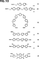
−図10は、n型エレクトロクロミック分子の化学式の例を示す。
−図11は、p型エレクトロクロミック分子の化学式の例を示す。
−図12は、結合したp型エレクトロクロミック基を持つ感光性試薬の分子式の例を示す。
以下でのアノードおよびカソードとしての電極の指定は、系の発色の過程におけるそれらの機能に関係する。説明される発色過程で適用する電圧は、カソードが負にアノードが正に分極するような電圧である。
1.エレクトロクロミック系(図1〜5)
1.1 外部電流−電圧源で光透過率を制御する透明エレクトロクロミック系(図1〜3)(I−aタイプ)。
このような系は平行で透明な2つの電極を含み、上記電極の各々の支持体1および8はそれぞれ導電性のプラスチックもしくはガラスのプレート、例えば、好ましくはドープされた、スズ酸化物2および7、またはインジウムおよびスズの酸化物で覆われた、ガラスプレートで作られて、接点9によって外部電気回路に接続される(図1〜3)。
電極の1つ(カソード)はナノ結晶質半導体、例えば厚さが0.3〜10μm、一例としては7μmの二酸化チタンの透明な層で構成される(図1〜3の参照符号3)。その表面は、図10(分子(1)〜(7))で定義され図1〜3(詳細図3a)の三角形の記号で示されるタイプの、吸着したエレクトロクロモフォリック分子の単分子層を含む。これらの分子は、第1に結合基、第2に酸化した状態(白い三角形)で可視光を吸収しないが還元した状態(黒い三角形)で可視光を吸収するエレクトロクロモフォリック基(n型エレクトロクロミック基)、並びに第3に場合によって1以上の重合性基または縮合性基を含む。2つの酸化状態の間のエレクトロクロミック基の酸化物還元電位は、半導体の導電バンドのレベルに近いもしくはそのレベルより負の電位、例えば二酸化チタンについては0〜−0.8Vでなければならない。結合基は、上記分子の半導体への吸着を可能にしなければならない。二酸化チタンの場合はエレクトロクロミック基として、例えば1以上のビオロゲン(4,4’−ジアルキル−ビピリジニウム)もしくはナフタレン−1,4,5,8−テトラカルボン酸基のジイミド、並びに結合基として、例えばカルボキシレート、サリチレート、カテコレート、またはホスホネートが使用できる。吸着が起こるとすぐに、重合性基、例えばビニルもしくはピロール基、または縮合性基、例えばアミンもしくはアルコール基は、上記分子が互いに結合して層が脱着しないようにできなければならない。
図1および2で示されるように他方の電極(アノード)は、ポリマー型で可逆的に酸化でき、還元した状態で無色であって酸化した状態でそれぞれ無色(図1)もしくは有色(図2)である透明材料の密な層6(および詳細6a)で作る。この材料の量は、少なくともカソードに吸着している全てのエレクトロクロミック基を還元するのに少なくとも必要な数の電子を取り出せるような量でなければならない。この材料は、例えば、酸化した状態で「プルシアンブルー」を作るポリ−フェロシアン化鉄(II)(「プルシアンホワイト」)であって、Itaya、AtakaおよびToshimaがJ.Am.Chem.Soc.1982,104,4767で説明する方法で電着させる。
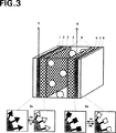
あるいは(図3)、アノードはナノ結晶質半導体の透明な層6から作られ、カソードに相似であり、およびその表面に吸着した分子(図3の詳細6aの正方形)の単分子層を持つ。上記吸着した分子は第1に結合基、第2に還元した状態(白い正方形)では可視光を吸収しないが酸化した状態(黒い正方形)で可視光を吸収するエレクトロクロモフォリック基(図11の分子(8)のようなp型エレクトロクロモフォリック基)、並びに場合によって第3に1以上の重合性基または縮合性基を含む。エレクトロクロミック基のこれらの2つの状態の間の酸化物還元電位は、半導体の導電バンドのレベルに近くなければならない、例えば二酸化チタンについては0〜−0.8Vでなければならない。エレクトロクロモフォリック基は、同様な電気化学的性質を持つが2つの酸化状態で無色の電気的に活性な原子基で置き換えてもよい。両方の電極がナノ結晶質でありエレクトロクロミック基を保持している場合、アノードおよびカソードは、初めにアノードおよびカソードが重合していないp型およびn型のエレクトロクロミック基をそれぞれ含んでいる状態で系を横切る脱着および拡散による任意の方式によって、共に吸着し平衡に達したn型およびp型両方のエレクトロクロミック基を持つことができる。2つのエレクトロクロミック基が共に吸着して2つの電極が同一であるこの系では、p型エレクトロクロミック基はカソードで不活性であってn型エレクトロクロミック基はアノードで不活性である。しかしながら分極に依存して、それぞれの電極はアノードまたはカソードのどちらとしても使用できる。
p型エレクトロクロモフォリック分子がアノードに存在する一般的な状態では、カソードにn型エレクトロクロモフォリック分子が無くてもよい。その場合その電気的な活性は、ナノ結晶質半導体への小さいカチオン、例えば二酸化チタンの場合はリチウム、の可逆的な挿入に基づく。
原理的に、全てのp型エレクトロクロミック基の酸化の後または最大量のカチオンの可逆的挿入の後でアノードによって放出される電子の数は、全てのn型エレクトロクロミック基の還元の後にカソードによって消費される電子の数に相当しなければならない。無色の状態のエレクトロクロミック基だけを含んでいなければならない系の初期状態を調節するために、またはこの無色の状態を回復させない続いて起こる系の偏りを修正するために、小さい補助電極を系に設けてもよい。溶媒または電解質の不可逆的な還元または酸化によって、この偏りを修正するような方法で電子をエレクトロクロミック電極に供給またはこの電極から引き出すことができる。
2つの電極の間の10〜100μm、例えば30μmの空間4(図1〜3)は、電気化学的に不活性な液体塩、または電気化学的に不活性で溶媒中に溶解している塩のいずれかで作る溶液で満たされており、場合により電極が間をあけるのを確実にするためにガラスビーズ5が加えられる。液体塩は例えばN,N’−ジアルキル−イミダゾリウム−、N,N’−ジアルキル−トリアゾリウム−、またはN−アルキル−チアゾリウムトリフルオロメタン−スルホネート(トリフラート(triflate))または−ビス(トリフルオロメチル)スルホニルアミド(ビス−トリフライルアミド(bis−triflylamide))型の塩でよく、他のアルキル基を保持することも保持しないこともある。溶媒中に溶解している電気化学的に不活性な塩は、上記液体塩の1つ、または固体塩、例えばリチウム−、テトラアルキルアンモニウム−、または1,3−ジアルキルイミダゾリウムビストリフライルアミド、−トリフラート、−ペルクロレート、または−ヘキサフルオロホスフェートでよい。溶媒は系の成分に対して安定な液、例えばアセトニトリル、ブチロニトリル、メトキシプロキオニトリル、グルタロニトリル、ジメチルスルホキシド、スルホラン、ジメチルホルムアミド、ジメチルアセトアミド、N−メチルオキサゾリジノン、ジメチル−テトラヒドロピリミジノン(DMPU)である。
従って本発明の1つの態様ではエレクトロクロミック系を、説明した構造で、SnO2の導電性ガラス上に7μmの厚さのナノ結晶質の二酸化チタンで作られたカソード、N−メチル−N’−(3−プロピルホスホネート)−ビピリジニウムブロマイド(図10の分子(1))から導かれたもの、無色の電気化学的に被覆したアノードをポリ−フェロシアン化鉄(II)のアノード、および電極の間の溶液としてグルタロニトリル中の0.3Mの濃度のリチウムビス−トリフライルアミドを使用して作製した。セルは接着性結合剤または加熱融解性ポリマーでシールする。電極の間に1Vの電圧を適用する場合、600nmでの系の吸光度は2秒間で0から1.5に変化し、見た目には無色透明から濃い青に変化する。この工程は、同じ時間間隔で可逆的である。
他の態様において、カソードに吸着する他の分子、すなわち最大吸光域での吸光度がビオロゲン1の2倍であるプロピルホスホネート基を備えた二量体のビオロゲン(図10の分子(2))を用いて同じ系を作製した。このような系では同じ条件において、550nmでの吸光度は2秒間で0から3に変化し、見た目には無色透明から濃い青に変化する。この工程は同じ時間間隔で可逆的である。
他の態様において、カソードに吸着する他の分子、すなわちビス−N,N’−[(3−カルボキシ−4−ヒドロキシフェニル)−4,4’]ビピリジニウムブロマイド6(図10の分子(3))を用いて同じ系を作製した。このような系では同じ条件において、同様に黄色ががかった透明から濃い緑に変化する。
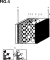
1.2 外部電流−電圧源で光の反射を制御する不透明エレクトロクロミック系(I−bタイプ、図4)
系の構造は1.1で説明した透明エレクトロクロミック系の構造と同様である(構成要素2および5、並びに詳細3aは図1〜3のそれらと同一である)。
カソードは、ナノ結晶質半導体の不透明層またはこの材料の透明層3で作られ、エレクトロクロミック基が無色の状態ならばどちらの場合にも拡散性反射体として機能するミクロ結晶質半導体の不透明層3’で内側の面を覆われる。
アノード8は電気化学的に酸化できる金属のプレート例えば亜鉛でできていて、上記金属は使用される溶媒に対して酸化した形で可溶であり、半導体の導電バンドの電位に近い電位で酸化できる。電極の間の溶液4は、高い濃度でアノードを構成する金属カチオンの塩を含有している。
あるいは1.1で説明したようにアノードは、導電性のプラスチックもしくはガラス上のプルシアンホワイトの付着物で作られる。
1つの態様において、カソードが厚さ7μmのナノ結晶質二酸化チタンでできている系を作製した。上記カソードはエレクトロクロミックセルの中に配置された面を、不透明の白いルチル形ミクロ結晶質二酸化チタンの層で覆われていた。アノードは亜鉛プレートでできている。電極の間の溶液は、1−エチル−3−メチル−イミダゾリウムビス−トリフライルアミド中に0.2Mの濃度の塩化亜鉛を含有している。装置の残部は、図10の吸収した分子(1)または(2)を用いる1.1で説明した態様と同一である。この系は、電極間に適用される電圧を0から1Vに上げたとき、反射による白い外見から反射による青い外見に2秒間で変化する。この過程は同じ時間間隔で可逆的である。電極を短絡して接続すると、これらの条件での亜鉛の酸化還元電位がビオロゲンエレクトロクロモフォリック基の酸化還元電位よりも低いために、系は青い熱力学的に最も安定な状態になる。系が有色の状態でも無色の状態でも、回路を開くと状態は数時間持続する。
2つの態様1.1または1.2のうちの1つにおいて、電極(導電性ガラスおよび半導体層)は、絶縁ストリップによって分断された導電性セグメントを確定するように彫り込んでもよい。側面の電気的な接続は、それぞれのセグメントを独立に制御することを可能にする。従って、記号、数字または文字の表示ができる装置の作製を可能にする。
2.フォトエレクトロクロミック系(図6〜9)
この装置は光の作用下でその色を変える特性を特徴とする。
系は2つの平行透明電極を含み、上記電極の支持体は導電性のプラスチックもしくはガラスのプレート、例えばインジウムおよびスズの酸化物またはドープされたスズ酸化物で被覆されたガラスプレートで構成される。
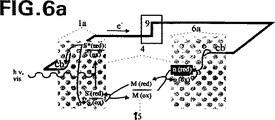
そのような系は内部電流−電圧源として、光−電流電極(図6〜8の参照符号1aおよび1b、および図9の参照符号1、2、3)(光アノード)を含む。1.1で説明したアノードに取って代わるこの電極は、カソードに関しては導電性のプラスチックもしくはガラスの層にナノ結晶質半導体層を被覆することによって作製する。光が当たると、光アノードは半導体の導電バンドcb(図6〜8)の電位で電子を生じる。これらの電子は、追加の電圧を提供しまたは提供せずに外部電気回路9によってカソード(図6〜8の参照符号6aおよび6b、図9の参照符号6、7、8)まで導電され、そこにおいてそれらは、半導体の導電バンドcbにより、吸着したn型エレクトロクロミック分子を還元する。電子は可逆的酸化性分子(図6および7のドナー15)、場合によってp型エレクトロクロミック基の酸化によって、光アノードに戻る。
一方、光の作用で発色を行う2つのタイプの系に異差をつけてもよい。
D.動的状態(図6および7):2つの酸化還元系、すなわち吸着したn型エレクトロクロミック基とドナーは直接または間接的に電気化学接触をしている。直接接触の場合、溶液中のドナーは非エレクトロクロミック電気化学媒体またはp型エレクトロクロミック基のどちらであってもよい。間接接触の場合、p型エレクトロクロミック基は吸着性基によってアノードに固定され、電気化学的な接触は溶解した非エレクトロクロモフォリック媒体か導電性ポリマーのいずれかで提供される。直接または間接の電子移動はn型エレクトロクロミック基を酸化させ可能なp型エレクトロクロミック基を還元させて、光によって起こったのと反対の過程である。2つの過程の競合は、結果として発色した状態のエレクトロクロミック基の所定の割合によって特徴付けられる系の定常的な動的状態をもたらす。このとき全体的な発色は、光の強度に対し自動的に非常に素早く適応する。系の反応性を決定する予備調整は、2つの逆工程の競合を制御するパラメータの調節によって行う。これらのパラメータは媒体または溶解したp型エレクトロクロミック基の濃度、これらの種の拡散(例えば溶媒粘度による)、電極間の距離、光アノードの光発電出力である。使用者は外部電気回路によって応答性を制御することができる。
P.持続状態(図8および9):2つの酸化還元系、すなわち吸着したn型エレクトロクロミック基およびドナーは電気化学的に接触していない。吸着性基によってドナーをカソードに固定すること、またはもしこのドナーが溶解しているならば、電極間の膜によってその拡散を阻止することのいずれがが可能である。このタイプの系は瞬間的な光照射の強度には適応しないが、光照射を始めてから最大量(飽和量)に達するまでに受けた光子の量に応じて変色し、それは光の強度がその後落ちても持続する。系は、エレクトロクロミック基を初期状態に戻す外部電流−電圧源の作用によって、無色の状態(削除)に戻せる。
一方、2つのタイプのアノード光電流活性を定義することができる。
UV:アノードの半導体は、紫外線(図7および8bのhνUV)によって直接励起される(バンドギャップの励起)。この場合ドナーは、半導体の価電子バンドでのホールの発生によって酸化する。
VIS原理:半導体は染料の吸着によって可視光(図6および8aのhνVIS)に対して感光性である。光電流アノードが露光すると、アノードに保持される染料は電子を半導体の導電バンドに送り込む。染料は可視光によって励起された状態で、電子をこの導電バンドに送り込めるように選択しなければならない。吸着を可能にする結合基、例えばホスホネート、カルボキシレート、サリチレート、またはカテコレートを備えたピリジンまたはポリピリジン型の芳香族配位子を含むルテニウム錯体が例えば使用できる。
更に、光アノードからカソードに向かう電子の流れを確実にするためおよび系を最適化するために、電流−電圧原またはダイオードを外部電気回路に備え付けることが必要なことがある。
従って本発明は、UVおよびVIS原理とDおよびP原理とを全ての可能なやり方で組み合わせることによって現実化される全てのフォトエレクトロクロミック系に関する。
2.1 自己適応フィルターまたは「インテリジェント」グレージング用の動的フォトエレクトロクロミック系(II−B)。
2.1.1 可視光に反応する系
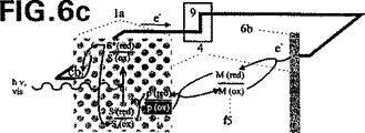
2.1.1.1 染料を伴うアノード、エレクトロクロミック基を伴うカソード(D−VIS、溶解したドナー、図6aおよび6b)
カソードは1.1で説明したように作製する。アノードは同様にナノ結晶質二酸化チタンの層を含むが、その色が簡単に知覚できず、それにより系の永続的な発色がないようにあらさ係数をカソードよりも10〜30倍小さくする。例えば、カソードのあらさ係数が1000である場合、あらさ係数が30〜100になるアノードを作製する。もしあらさ係数が厚さに対して線形に変化するなら、例えば10μmの厚さのカソードに対してアノードは0.3〜1μmの厚さに相当する。
アノードの染料Sの量はカソードのn型エレクトロクロミック基の量よりもはるかに少ないので、カソードのエレクトロクロミック基の全部を還元するためにそれぞれの染料分子は数回の電子注入サイクルを行わなければならない。それそれの電子注入の後で酸化された染料S+を還元できるように、溶解した電気化学媒体15が存在しなければならない。従って、その酸化還元電位は染料のそれよりも小さくなければならない。露光が終わったときに系が無色の初期状態に戻るためには、酸化した形の電気化学媒体は還元されたエレクトロクロミック基を酸化させることができなければならない。しかしながらこの工程は、露光しているときに系の達成する定常状態が高い割合の還元されたエレクトロクロミック基を特徴とするように十分にゆっくりであるべきである。工程の速度論を調整する一つの実際の方法は、溶液4の粘度を変化させることである。液体塩は、これを行うために大変ふさわしい溶媒である。
様々な態様において、電気化学媒体としてp型エレクトロクロミック基を使用することができる(図6d)。
現実化の例では、0.3μmのナノ結晶質二酸化チタン層で作る光電流アノードは、吸着した染料としてルテニウム錯体、例えばシス−ジチシアナト−ビス−(2,2’−ビピリジル−4,4’−ジカルボキシラト)−ルテニウム(II)または4,4’,4’’−トリメチル−テルピリジン−ホスホナトテルピリジンルテニウム(II)を保持する。カソードは7μmのナノ結晶質二酸化チタン層で作り、図10の分子(1)のような吸着したエレクトロクロミック分子を保持する。電極間の溶液は、1.1で説明した液体塩、例えば1−エチル−2−メチル−イミダゾリウムビス−トリフライルアミド中の、コバルト錯体の塩、例えばトリス−フェナントロリン−コバルト(II)トリフルオロメタンスルホネート、およびリチウム塩、例えばビスフライルアミドを含む。模擬的な太陽光(AM1.5)で、この系は青色になり、600nmの光を90%より多く吸収する。露光をやめると、系は無色に戻る。
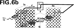
2.1.1.2 染料に結合したp型エレクトロクロモフォリックドナーを伴うアノード、n型エレクトロクロミック基を伴うカソード(D−VIS、図6b)。
このような系は、2つの電極1aおよび6aのあらさ係数が100〜1500例えば700で原則的に同一であること、およびカソードに吸着している染料Sが共有結合によってこの染料に結合しているp型エレクトロクロミック基を保持することを除いて、2.1.1.1のように構成する。
光アノードを可視光(hνVIS)で露光する場合、アノードに保持される染料は半導体の導電バンドに電子を注入して、直接的にp型エレクトロクロモフォリック基を酸化して発色させる。電子は、半導体の導電バンドによって吸着したエレクトロクロミック分子を還元するカソードまで電気回路によって導電される。
原理的に、全てのp型エレクトロクロミック基の酸化後にアノードによって送り出される電子の数は、全てのn型エレクトロクロミック基の還元後はカソードによって消費される電子の数に匹敵しなければならない。
このような系は、露光している状態および露光していない状態の両方で自然に発色している。露光しない場合の発色は染料による吸光に起因し、露光している場合は酸化したp型エレクトロクロミック基および還元したn型エレクトロクロミック基の吸収が加わる。
電極間の液は、酸化還元電位がp型エレクトロクロミック基とn型エレクトロクロミック基の間にある電気化学媒体で作る。その濃度、および原則的に等しい酸化した形のものと還元した形のものの割合は、露光をやめたときに系が初期の無色の状態に戻るように調節する。しかしながらこの工程は、露光しているとき系によって達成される定常状態が高い割合の還元したn型エレクトロクロミック基と酸化したp型エレクトロクロミック基によって特徴付けられるように十分ゆっくりでなければならない。工程の速度論を調整する一つの実際の方法は、液の粘度を変えることからなる。液体塩はこれを行うのに非常にふさわしい溶媒である。
1つの態様において、吸着した分子(図12の分子(9)または(10))として、ルテニウム錯体例えばビス−テルピリジンルテニウムを保持する光電流アノードを7μmのナノ結晶質二酸化チタン層で作る。上記分子は結合基、例えばホスホネート基を持ち、並びにp型エレクトロクロモフォリック基、例えば(ビス(4’,4’’−メトキシフェニル)アミノ−4−フェニル(分子(9)について)または(ビス(4’,4’’−メトキシフェニル)アミノ−4−フェノキシメチル(分子(10)について))に結合している。7μmのナノ結晶質二酸化チタン層から作るカソードは吸着したn型エレクトロクロモフォリック分子、例えば図10の分子(1)の単分子層を保持している。電極間の液は、1.1で説明した液体塩、例えば1−エチル−2−メチル−イミダゾリウムビス−トリフライルアミド中の、コバルト(II)およびコバルト(III)の形のコバルト錯体塩、例えばトリス−フェナントロリン−コバルトトリフルオロメタンスルホネート、およびリチウム塩、例えばビス−トリフライルアミドを含む。模擬的な太陽光(AM1.5)で露光すると、この系はオレンジ色から緑色に変化し、600〜750nmの光を90%より多く吸収する。露光をやめると系はオレンジ色に戻り、600〜750nmでの吸光率は10%より小さい値に戻る。
2.1.1.3 共に吸着したエレクトロクロモフォリック基を伴うアノード(D−VIS、図6b)。
この様な系は、p型エレクトロクロモフォリック基が共役結合によって染料に結合しておらず、染料を共に光アノードに吸着し同様に結合基を持つ別の分子を構成することを除いて、2.1.1.2のように作る。染料によるp型エレクトロクロミック基の酸化工程は、2.1.1.2のように分子内ではなく、分子間である。染料がいくつかの共に吸着したp型エレクトロクロミック分子を連続して酸化することが可能ならば、露光されない系の発色を制限するように染料よりも多くのエレクトロクロモフォリック分子を吸着させることができる。
電極間の溶液は、2.1.1.1で説明したものと同一である。
1つの態様において光電流アノードは、吸着した分子として第一に、結合基、例えばホスホネートを持つルテニウム錯体、例えばビス−テルピリジンルテニウム、および第二にp型エレクトロクロモフォリック分子、例えば図11の分子(8)を保持する7μmのナノ結晶質二酸化チタン層で作る。エレクトロクロモフォリック分子の表面濃度は染料のそれの2倍ほどであり、染料1に対してエレクトロクロモフォリック基2である濃度比率の2つの分子の溶液に浸漬することによって電極を感受性にすることで得られる比率である。7μmのナノ結晶質二酸化チタン層で作られたカソードは、吸着したn型エレクトロクロモフォリック分子、例えば図10の分子(1)の単分子層を保持する。電極間の溶液は2.1.1.2で説明したものと同一である。模擬的な太陽光(AM1.5)で露光すると、この系は非常に明るいオレンジ色から濃い青色に変化し、600〜750nmの光を90%より多く吸収する。露光をやめると系は初期の状態に戻り、600〜750nmでの吸光率は10%より小さい値に戻る。
2.1.1.4 染料に結合したp型エレクトロクロモフォリックドナーを伴うアノード、エレクトロクロミック基を伴わないカソード(D−VIS、図6c)。
2.1.1.2および2.1.1.3で説明した装置は、半導体の層も吸着した分子も保持しない導電性のプラスチックもしくはガラス(透明な態様)、または金属(不透明な態様)のカソード6bで現実化することもできる。従って系は、電気化学媒体として溶解したp型エレクトロクロミック基を含むことができる。
2.1.2 紫外線に反応する系
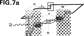
2.1.2.1 アノードに吸着したp型エレクトロクロミック基、カソードに吸着したn型エレクトロクロミック基(D−UV、図7a)
紫外線に反応する系を得るためには、光アノード1bに還元した状態で無色であり酸化した状態で有色(p型エレクトロクロミック基)のエレクトロクロモフォリック分子の単分子層を吸着させ、カソード6aにn型エレクトロクロモフォリック分子の単分子層を吸着させることがふさわしい。2つの電極のあらさ係数は100〜1500例えば700で原則的に同一である。原理的に、全てのp型エレクトロクロミック基の酸化の後でアノードによって送り出される電子の数は、全てのn型エレクトロクロミック基の還元の後にカソードによって消費される電子の数に相当すべきである。
光アノードに近紫外線(hνUV)(350〜420nm)を照射する場合、半導体の価電子バンド電子の導電バンドへの励起は、約3Vの電位のいくらかの「正孔」をこの価電子バンドに発生させ、これがp型エレクトロクロミック基を酸化して発色させる。電子は、半導体の導電バンドを経由して吸着したエレクトロクロミック分子を還元するカソードまで電気回路9によって導かれる。
電極間の溶液は電気化学媒体15から作られ、その酸化還元電位はp型エレクトロクロミック基のそれとn型エレクトロクロミック基のそれの中間である。その濃度並びに原則的に等しい酸化したものと還元したものの割合は、露光をやめるときに系が初期状態、つまり無色に戻るように調整する。しかしながらこの工程は、露光している場合には十分に遅く、系によって達成される定常状態が還元したn型エレクトロクロミック基と酸化したp型エレクトロクロミック基の大きい割合によって特徴付けられるように十分遅くなければならない。工程の速度論を調整する1つの現実的な方法は、溶液の粘度を変えることである。液体塩はこれを行うのに非常にふさわしい溶媒である。
1つの態様において、光電流アノードは7μmのナノ結晶質二酸化チタン層で作られ、これ吸着したp型エレクトロクロモフォリック分子として結合基を持ったトリアリールアミン、例えばナトリウム(ビス(4’,4’’−メトキシフェニル)アミノ−4−フェノキシ)−3−プロピルホスホネート(図11の分子(8))を保持する。7μmのナノ結晶質二酸化チタン層で作られたカソードは、吸着したn型エレクトロクロミック基、例えば図10の分子(1)を保持する。電極間の溶液は、2.1.1.2で説明したものと同一である。
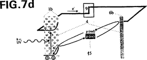
2.1.2.2 p型エレクトロクロモフォリックドナーを伴うアノード、エレクトロクロミック基を伴わないカソード(D−UV、図7b)
2.1.2.1で説明した装置は、半導体の層も吸着した分子も保持しない導電性のプラスチックもしくはガラス(透明な態様)、または金属(不透明な態様)のカソード6bで現実化することもできる。従って系は、電気化学媒体15として溶解したn型エレクトロクロミック基を含むことができる。
2.1.2.3 エレクトロクロモフォリックドナーを伴わないアノード、n型エレクトロクロミック基を伴うカソード(D−UV、図7c)
2.1.2.1で説明した装置は、半導体が吸着したエレクトロクロモフォリック分子の層を全く保持しないアノード1bで現実化することもできる。従って半導体の価電子バンドの正孔は溶解した電気化学媒体15を直接酸化し、上記電気化学媒体がカソード6aの還元したn型エレクトロクロミック化合物を酸化する。
2.1.2.4 エレクトロクロモフォリックドナーを伴わないアノード、エレクトロクロミック基を伴わないカソード、溶解した電気化学媒体p型エレクトロクロミック基(D−UV、図7d)
2.1.2.3で説明した装置は、半導体の層も吸着した分子も保持しない導電性のプラスチックもしくはガラス(透明な態様)、または金属(不透明な態様)のカソード1bで現実化することもできる。従って電気化学媒体15はp型エレクトロクロミック基である。
2.2 可逆性データ記憶用の持続性フォトエレクトロクロミック系(III−A)(図8および9)
2.2.1 可視光に反応する系(P−VIS、図8aおよび9)
装置は電圧を加えたときに、光の影響下でその色を変える性質を特徴とする。露光に関わらず、電圧を逆にするとそれは初期状態に戻る。
系は、電流−電圧源9を持つ電気回路によって接続された2.1で説明されたような2つの透明または不透明な平行電極を含む。
2.2.1.1 透明系
吸着した分子を伴うアノード1a(図8a)または1、2、3(図9)は、2.1.1.2で説明したもの(図12の(9)および(10)タイプの吸着した分子で長方形(発色基)および正方形(p型エレクトロクロミック基)によって図9の詳細3aに示される)、または2.1.1.3で説明したようなもの(図11の(8)タイプの吸着した分子、と結合基を備えたルテニウム錯体の両方の吸着)と類似の方法で作る。これらの分子に加えて、吸着したp型エレクトロクロミック基を互いに絶縁する電気化学的に不活性な分子を、情報の局所的な閉じ込めを妨げるこれらのエレクトロクロミック基の間の電子の移動を避けるように、共に吸着させることが必要なことがある。
カソードは単分子層で覆わないことを除いて1.1で説明したように作る。電極4の間の溶液は、1.1で説明したように溶媒に溶解し可逆的に半導体に入り込むことができるイオンの塩を含む。光ビーム10(図9)、例えばレーザーがアノードのある領域に達すると、その部位の染料は電子を半導体の導電バンドに入れ、酸化された染料はそれに結合したp型エレクトロクロミック基をすぐに酸化する。適用した電圧の作用下で、電子はアノードから引き抜かれてカソードに伝導され、そこでカチオンの挿入を可能にする。
1つの別態様においてはでカソードを、n型エレクトロクロミック基(図8a)または2つの酸化状態が無色の(n型エレクトロクロモフォリック要素がない)電気的に活性な吸着性分子の単分子層で覆うことを除いて、1.1で説明したように作製する。この場合、アノードから引き抜かれてカソードに伝導される電子は、エレクトロクロモフォリック分子であってもそうでなくても電気的に活性な分子を還元することができる。
もう1つの他の態様(図9)においてカソードは、可逆的に酸化できるタイプであり両方の酸化状態において無色であるポリマーの透明材料6の密な層から作る。この場合、アノードから引き抜かれてカソードに伝導される電子は、ポリマーを還元することができる。
露光した場所のエレクトロクロモフォリック分子の酸化によって発生する局所の発色は、電極間の電圧を消去して短絡を起こすことによってなくし、逆の電圧を適用することによってもなくすことができる。
1つの態様において、結合基、例えばホスホネートを持ち、p型エレクトロクロモフォリック基、例えば(ビス(4’,4’’−メトキシフェニル)アミノ−4−フェニル(分子(9)について))または(ビス(4’,4’’−メトキシフェニル)アミノ−4−フェノキシメチル(分子(10)について)と結合したルテニウム錯体、例えばビス−テルピリジンルテニウムを、吸着した分子(図12の分子(9)または(10))として保持する7μmのナノ結晶質二酸化チタン層でアノードを作る。カソードは7μmのナノ結晶質二酸化チタン層で作る。電極間の溶液はリチウム塩、例えばビス−トリフライルアミドを、1.1で説明したような液体塩、例えば1−エチル−2−メチル−イミダゾリウムビストリフライルアミドで含む。アノードが正でカソードが負に帯電するように系に0.5Vの電圧をかけると、1サン(AM1.5)の強度の白色光による一分間の局所的な露光は、露光された一部の領域でのみオレンジ色から緑色への変色をもたらす。系は回路を開いてこの状態を数時間維持することができる。−0.5Vの電圧を適用することによって初期状態に戻すことができる。
2.2.1.2 不透明系
系は、アノードに関することを除いて2.2.1で説明するような透明フォトエレクトロクロミック系と同一である。これはナノ結晶質半導体の不透明層から作る。
1つの態様においてはアノードを、7μmのナノ結晶質二酸化チタンで作り、吸着する分子(図12の分子(9)および(10))を保持させるのに並んで、セルの内側に配置された面を不透明で白色のルチル型のミクロ結晶質二酸化チタン層で覆う。装置の残部は2.2.1で説明した態様と同一である。不透明アノードによって全体が被覆され、起こりうる発色がアノードで行うデータの書き込みおよび記憶の工程を妨げないので、この系はカソードにn型エレクトロクロミック基が存在することよりよく適合する。
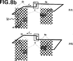
2.2.2 紫外光に反応する系(P−UV、図8b)
カソードが吸着した染料ではなくp型エレクトロクロモフォリック化合物を保持する状態で、この系は可視光に反応する2.2.1で説明した系と同じような様式で紫外光に反応する。The present invention relates to an electrochromic or photoelectrochromic device, which is particularly suitable for reversible storage and display of data and control of light transmission, and uses one or two electrodes made of a semiconductor with a large specific surface area. .
Foreword
In order to make electrochromic devices where the change in visible light absorption is greater than 90% (
-The electrochromic compound is present in the solution in contact with the electrode. The requirements are fully met with a concentration of 0.25 M and a layer thickness of 2 μm solution.
Electrochemically depositing the electrochromic compound on the electrode in a thin layer.
Polymerizing the electrochromic compound or impregnating the surface of the polymer or composite membrane;
In the following, a new type of electrochromic and photoelectrochromic device will be described. These devices use electrodes made of nanocrystalline semiconductors with a very large specific surface area on which electrochromic molecules are adsorbed to achieve the performance characteristics shown above To do. These devices can obtain vivid colors quickly, such as switching times shorter than 3 seconds for changes in absorbance of at least 90%.
Description of the invention
The present invention relates to an electrochemical system comprising at least two electrodes, each of which may be transparent or opaque, at least one of which changes color depending on the following I-III.
I. A voltage applied between two electrodes by a current-voltage source.
II. The intensity of light at which the system is exposed.
III. Action of the combination of I and II.
Furthermore, the following color changes A and B may be caused by light.
A. The color changes locally, that is, only at the exposed location.
B. The color changes throughout the system, i.e. regardless of where it is exposed.
Furthermore, the following a and b may be used as the color change caused by the external voltage.
a. The overall color, ie the color of the entire system, changes.
b. The color changes only locally, i.e. where it is electrically involved (organized surface of the electrode).
This results in the following applications:
Ia: A reversible electrochromic system for managing light transmittance, controlled by an external voltage-current source.
Ib: Electrochromic system displaying reversible data, controlled by external voltage-current source.
III-A: Reversible photoelectrochromic system with optical writing and reversible data storage, limited by light (writing) and external voltage-current source (storage and deletion).
II-B: A system that automatically adapts to the intensity of light received by the transmittance (filter, transparent plate glass).
All these color changes are readily observable with the naked eye, except in the case of III-A, where data storage is performed in submicron sizes, and are well defined chemical reactions at the molecular level, ie electrochromic compounds This corresponds to the oxidation or reduction of an electrochromic compound that is usually fused to the entire surface of an electrode made of a nanocrystalline semiconductor to which molecules such as are accessible. Such electrodes do not vary by more than 5% while maintaining the relative humidity of the ambient air at 50-80% during the hydrolysis of the metal alcoholate of the metal from which the oxide is prepared. Electrochem. Soc. Prepared by a sol-gel method as described in detail in 1979, 126, 2007. The thickness of the nanocrystalline layer is 0.1 to 10 μm or thicker so that the roughness coefficient is about 10 to 1000, for example 700. This roughness coefficient means that the electrode surface area accessible to molecules having a major diameter of 1 nm is 10 to 1000 times, for example 700 times, the value of the projection layer surface. As a result, all changes in the optical properties of the molecular layer adsorbed on the semiconductor surface generate a macroscopic effect that is amplified by the roughness coefficient. Thus, light absorption by the monolayer of colored molecules is enhanced over a flat surface at a rate equal to the roughness coefficient of the nanocrystalline electrode.
A semiconductor that is particularly suitable for the preparation of nanocrystalline electrodes must have a large band gap. They are group IV elements of the periodic table, such as titanium, zirconium or hafnium, group V elements such as vanadium, niobium or tantalum, group VI elements such as chromium, molybdenum or tungsten, or other groups. It may be selected from oxides of elements such as silver, zinc, strontium, iron or nickel. Similarly, SrTiO Three Or CaTiO Three Perovskite type may be used.
In particular, the present invention relates to an electrochromic or photoelectrochromic device having the property of changing color due to the effect of voltage and / or light intensity changes. The apparatus comprises at least one cathode and one anode, wherein at least one of these electrodes comprises a conductive or at least partly transparent or translucent substrate, and these An electrolyte disposed between the electrodes, and an electrical circuit connecting the cathode and anode. The device includes a coating comprising at least one nanocrystalline layer of at least one semiconductor material having at least one roughness coefficient of at least 20 and an electrically active molecule or electrically active A monolayer of a polymer that retains the monolayer adsorbed on the surface of the coating and that the device is optionally at least one auxiliary electrically active that dissolves in the electrolyte. It is a compound, Comprising: The compound which has the characteristic which can be reversibly oxidized or reduced is characterized by the above-mentioned.
In particular, it is possible to envision embodiments that provide one or more of the following specific features.
a. The semiconductor is titanium, zirconium, hafnium, vanadium, niobium, tantalum, molybdenum, tungsten, zinc, strontium, iron, nickel, silver oxide, or a perovskite of the above metal.
b. The electrical circuit includes a current-voltage source.
c. The device includes a small auxiliary electrode in addition to the anode and cathode.
It is particularly possible to achieve several alternative embodiments of the electrochromic device of the present invention, each of these alternative embodiments providing specific features described in one of the following points.
1. The cathode carries an adsorbed monolayer of at least one type of electrochromophoric molecule, and the molecule is at least one adsorptive linking group, possibly a polymerizable or condensable group, and colorless in an oxidized state. Containing at least one n-type electrochromophoric group colored in a reduced state, with an auxiliary electrically active compound fixed to the anode in the form of an electrically active film, between the electrodes In another embodiment, the electrolyte solution of (1) contains at least one electrochemically inert salt dissolved in a solvent.
2. The other aspect of the
3. The electrochromophoric molecule contains a carboxylate, salicylate, catecholate or phosphonate group as an attachment group and, if applicable, a vinyl or pyrrole group as a polymerizable group, or an alcohol or amine group as a condensable group Another aspect described in
4). The other aspect according to
5). The alternative embodiment of
6). 6. Another embodiment according to
7). 7. Another embodiment according to
8). 8. Another aspect according to
9. The other aspect according to
10. 10. An alternative embodiment according to
11. 10. Another embodiment according to
12 10. Another aspect of
13. The electrically active film is composed of a nanocrystalline semiconductor layer having a roughness coefficient greater than 20, and an electrically active molecule or an electrically active polymer monomolecular layer is adsorbed on the surface of the semiconductor. Another aspect described in
14 The electrically active molecule contains an adsorptive linking group, optionally a polymerizable or condensable group, and a p-type electrochromophoric group that is colorless in the reduced state and colored in the oxidized state. 14. Another embodiment according to point 13, which is an electrochromophoric molecule.
15. 15. The other aspect according to point 14, wherein the electrochromophoric molecule includes the bonding group and the polymerizable group according to
16. The other aspect of the
17. The other aspect according to
18. 18. The point 17 according to point 17, wherein the liquid salt is a liquid salt of 1-ethyl-3-methylimidazolium- or 1-propyl-2,3-dimethylimidazolium trifluoromethanesulfonate or -bis (trifluoromethylsulfonyl) amide. Another aspect.
19. The other aspect according to
20. The electrochemically inert salt is tetraalkylammonium-, 1,3-dialkylimidazolium-, or lithium hexafluorophosphate, -trifluoromethanesulfonate, -bis (trifluoromethylsulfonyl) amide, or -perchlorate. Another aspect of
Similarly, it is particularly possible to achieve several alternative embodiments of the photoelectrochromic device of the present invention, each of these alternative embodiments providing specific features described in one of the following points.
21. Another aspect in which the color of the device automatically adapts to the light intensity.
22. The anode holds a nanocrystalline semiconductor layer having a roughness coefficient greater than 20, the semiconductor is due to the above point a, and a monomolecular layer of a photosensitive reagent is adsorbed on the semiconductor surface. 22. Another embodiment of point 21, wherein said comprises a chromophoric group, an adsorptive binding group, and optionally a polymerizable or condensable group.
23. The anode holds a nanocrystalline semiconductor layer having a roughness coefficient greater than 20, which is due to the point a described above, and a monolayer of electrochromophoric molecules is adsorbed on the semiconductor surface, and the molecule 23. The alternative embodiment of point 21, wherein the compound comprises an adsorptive binding group, a reduced, colorless and oxidized p-type electrochromophoric group, and optionally a polymerizable or condensable group.
24. The alternative embodiment according to point 21, wherein the anode has a nanocrystalline semiconductor layer with a roughness coefficient greater than 20, the semiconductor being due to point a and having no adsorbed molecules.
25. 23. Another embodiment according to point 22, wherein the photosensitive reagent contains a p-type electrochromophoric group bonded to a chromophoric group that is colorless and oxidized in a reduced state and has a colored property.
26. 23. Another embodiment according to point 22, wherein the photosensitive reagent and the electrochromophoric molecule are both adsorbed to the anode in a ratio of 1: 1, 1: 2, or 1: 5 or greater.
27. The cathode holds a nanocrystalline semiconductor layer having a roughness coefficient greater than 20, which is due to the point a described above, and a monolayer of at least one type of electrochromophoric molecule is present on the semiconductor surface. Adsorbed and the molecule has at least one adsorptive linking group, at least one n-type electrochromophoric group that is colorless and reduced in color in an oxidized state, and optionally a polymerizable or condensable group. Another aspect of point 21 including.
28. 22. Another embodiment according to point 21, wherein the cathode does not hold any nanocrystalline semiconductor layer.
29. 22. Another embodiment according to point 21, wherein the electrically active auxiliary compound is an electrochemically active salt dissolved in the solution capable of transporting electrons between the anode and cathode.
30. The electroactive auxiliary compound is a p-type electrochromophoric group bonded to the chromophoric group described in point 25, and the solution contains only an electrochemically inactive salt. Aspect.
31. 30. Another embodiment according to point 29, wherein the electrochemically active salt is a dissolved p-type or n-type electrochromic group.
32. 28. Another embodiment according to points 22, 23, and 27, wherein the electrochromophoric molecule comprises a linking group and a polymerizable group as described in
33. 23. Another embodiment according to point 21, which advantageously accommodates visible light in which the cathode is made according to point 27 and the anode is made according to point 22.
34. 40. Another embodiment according to
35. 34. Another embodiment according to
36. 22. Another embodiment according to point 21, wherein the cathode is made according to point 27 and the solution is advantageously adapted for visible light made according to point 29.
37. 37. Another embodiment according to point 36, wherein the anode is advantageously adapted to visible light made according to point 25.
38. 37. Another embodiment according to point 36, wherein the anode is advantageously adapted to visible light made according to point 26.
39. 26. An alternative embodiment according to point 21, advantageously adapted for ultraviolet light, wherein the cathode is made according to point 27, the anode is made according to point 23, and the solution is made according to point 29.
40. An alternative embodiment according to point 21, wherein the cathode is made according to point 27 and the solution is advantageously adapted to ultraviolet light made according to point 29.
41. 26. Alternative embodiment according to point 21, wherein the cathode is made according to point 28, the anode is made according to point 23, and the solution in which the dissolved electrochromic group is p-type is advantageously adapted to ultraviolet light made according to point 31 .
42. 22. Another embodiment according to point 21, wherein the cathode is advantageously made according to point 28, and the solution in which the dissolved electrochromic group is p-type is advantageously adapted to ultraviolet light made according to point 31.
43. 22. Another embodiment according to point 21, which can be used advantageously for reversible data storage in which the cathode is made according to point 27 and the solution is made according to point 30.
44. 22. Another embodiment according to point 21, which can be used advantageously for reversible data storage, wherein the solution is made according to point 30 and a reflective screen is arranged behind the anode.
45. 45. An alternative embodiment as set forth in point 44, wherein the reflective screen is made of a microcrystalline semiconductor layer, the semiconductor being from point a above and attached to the surface of the anode located inside the system.
46. The solution is made according to point 30, the cathode is made of a dense layer of electrically active material that can be reversibly reduced, and the dense layer is attached to a layer of conductive plastic or glass 22. Another aspect according to point 21, which can be used advantageously for data storage.
47. 47. Another embodiment according to point 46, wherein the dense layer can be advantageously used for reversible data storage, which is an electrically active organic polymer or a composite material comprising an electrically active material.
48. 48. Another embodiment according to points 43 to 47, wherein the anode can advantageously be used for reversible data storage responsive to visible light made according to point 22.
49. 48. Another embodiment according to points 43 to 47, wherein the anode can advantageously be used for data storage responsive to visible light made according to point 25.
50. 48. Another embodiment according to points 43 to 47, wherein the anode can be advantageously used for data storage responsive to visible light made according to point 26.
51. 48. Another embodiment according to any of points 43 to 47, wherein the anode can advantageously be used for data storage responsive to ultraviolet light made according to point 23.
52. An alternative embodiment according to point 21, wherein the solvent is an electrochemically inert liquid salt according to point 18, or another liquid according to point 19.
53. 22. Another embodiment according to point 21, wherein one of the electrochemically inert electrolytes is selected according to
Similarly, the present invention particularly relates to electrochromophoric compounds and photosensitive reagents described in the following points.
54.1 Made of one or more viologen groups (4,4'-dialkyl-bipyridinium) linked by one or more alkyl chains, which may contain one or more phenylene groups, terminated by a phosphonate, salicylate, or catecholate group The n-type electrochromophoric compound according to
55. 55. The n-type electrochromophoric compound according to point 54, further comprising a pyrrole, thiophene, vinyl, alcohol, or amine group.
56.1 Made of one or more diimides of naphthalene-1,4,5,8-tetracarboxylic acid groups linked by one or more alkyl chains that may contain one or more phenylene groups, and phosphonate, salicylate, or catecholate groups The n-type electrochromophoric compound according to
57. 57. The n-type electrochromophoric compound according to point 56, further comprising a pyrrole, thiophene, vinyl, alcohol, or amine group.
58. 58. The n-type electrochromophoric compound according to points 54 to 57, which represents the structure below.
The p-type electro of point 14 made of one or more triarylamine groups joined by one or more alkyl chains, which may contain 59.1 or more phenylene groups, and terminated with a phosphonate, salicylate or catecholate group Chromophoric compound.
60. 60. The p-type electrochromophoric compound according to point 59, further comprising a pyrrole, thiophene, vinyl, alcohol, or amine group.
61. 61. A p-type electrochromophoric compound according to points 59 and 60 as represented by molecule (8) in FIG.
62. 26. A photosensitive reagent compound which binds to one or more p-type electrochromophoric groups according to point 25, wherein the compound is a ruthenium complex containing a polypyridine ligand, and at least one of the polypyridine ligands is one or more phosphonates. A photosensitive reagent compound having a carboxylate, salicylate or catecholate group, and at least one triarylamine group.
63. 65. A photosensitive reagent compound bound to one or more p-type electrochromophoric groups according to
64. 64. A photosensitive reagent compound bound to one or more p-type electrochromophoric groups at
Example description
The following description given by way of example relates to the figure, in which:
FIG. 1 shows a first embodiment of the transparent electrochromic device of the invention.
FIG. 2 shows a second embodiment of the transparent electrochromic device of the invention.
FIG. 3 shows a third embodiment of the transparent electrochromic device of the present invention.
FIG. 4 shows an example of an opaque electrochromic device.
FIG. 5 shows the feasibility of fabricating an opaque electrochromic device in which a cathode for reversible data display is constructed.
-Figures 6a-6d show different aspects of the dynamic type photoelectrochromic device (D-VIS) of the present invention responsive to visible light.
-Figures 7a-7d show different aspects of the dynamic type photoelectrochromic device (D-UV) of the present invention that is sensitive to ultraviolet light.
-Figures 8a and 8d show different aspects of the persistent type (D-VIS) responsive to visible light (D-VIS) (Figure 8a) and the persistent type responsive to ultraviolet light (D-UV) (Figure 8b) photoelectrochromic devices. .
FIG. 9 shows a photoelectrochromic device of the present invention for reversible data storage and writing.
FIG. 10 shows an example of the chemical formula of an n-type electrochromic molecule.
FIG. 11 shows examples of chemical formulas for p-type electrochromic molecules.
FIG. 12 shows an example of the molecular formula of a photosensitive reagent having a p-type electrochromic group attached.
The designation of the electrodes as anode and cathode below relates to their function in the process of color development of the system. The voltage applied in the described color development process is such that the cathode is negatively polarized and the anode is positively polarized.
1. Electrochromic system (Figures 1-5)
1.1 Transparent electrochromic system (FIGS. 1 to 3) (Ia type) for controlling light transmittance with an external current-voltage source.
Such a system comprises two parallel and transparent electrodes, each
One of the electrodes (cathode) is composed of a nanocrystalline semiconductor, for example, a transparent layer of titanium dioxide having a thickness of 0.3 to 10 μm, for example 7 μm (
As shown in FIGS. 1 and 2, the other electrode (anode) can be oxidized reversibly in a polymer form, colorless in the reduced state and colorless (FIG. 1) or colored (FIG. 2) in the oxidized state, respectively. Made of a dense layer 6 (and details 6a) of transparent material. The amount of this material must be such that at least the number of electrons necessary to reduce all the electrochromic groups adsorbed on the cathode can be removed. This material is, for example, poly-ferrocyanide (II) ("Prussian white") that forms "Prussian blue" in the oxidized state, and Itaya, Ataka and Toshima are described in J. Am. Am. Chem. Soc. Electrodeposition is performed by the method described in 1982, 104, 4767.
Alternatively (FIG. 3), the anode is made from a
In the general state where p-type electrochromophoric molecules are present at the anode, the cathode may be free of n-type electrochromophoric molecules. In that case, the electrical activity is based on the reversible insertion of small cations into the nanocrystalline semiconductor, for example lithium in the case of titanium dioxide.
In principle, the number of electrons released by the anode after oxidation of all p-type electrochromic groups or after reversible insertion of the maximum amount of cations is determined by the cathode after reduction of all n-type electrochromic groups. It must correspond to the number of electrons consumed. To adjust the initial state of the system, which must contain only the colorless electrochromic group, or to correct the subsequent system bias that does not restore this colorless state, a small auxiliary electrode is used in the system. May be provided. By irreversible reduction or oxidation of the solvent or electrolyte, electrons can be supplied to or extracted from the electrochromic electrode in a manner that corrects this bias.
A space 4 (FIGS. 1 to 3) of 10-100 μm, for example 30 μm, between the two electrodes is used for the electrochemically inert liquid salt or the salt that is electrochemically inert and dissolved in the solvent.
Accordingly, in one embodiment of the present invention, an electrochromic system has the structure described, SnO 2 N-methyl-N ′-(3-propylphosphonate) -bipyridinium bromide (molecule (1) in FIG. 10), cathode made of 7 μm thick nanocrystalline titanium dioxide on a glass of conductive glass A colorless electrochemically coated anode as a solution between poly-iron (II) ferrocyanide anode, and an electrode at a concentration of 0.3M lithium bis-trifylamide in glutaronitrile It was prepared using. The cell is sealed with an adhesive binder or a heat-meltable polymer. When a voltage of 1V is applied between the electrodes, the absorbance of the system at 600 nm changes from 0 to 1.5 in 2 seconds and changes from colorless and transparent to dark blue. This process is reversible at the same time interval.
In another embodiment, another molecule adsorbed on the cathode, ie, a dimeric viologen having a propylphosphonate group having an absorbance at the maximum absorption region twice that of viologen 1 (molecule (2) in FIG. 10) is used. The same system was made. In such a system, under the same conditions, the absorbance at 550 nm changes from 0 to 3 in 2 seconds, and visually changes from colorless and transparent to dark blue. This process is reversible at the same time interval.
In another embodiment, other molecules adsorbed on the cathode, ie bis-N, N ′-[(3-carboxy-4-hydroxyphenyl) -4,4 ′] bipyridinium bromide 6 (molecule (3) in FIG. 10) The same system was made using In such a system, under the same conditions, the color changes from yellowish transparent to dark green.
1.2 Opaque electrochromic system that controls reflection of light with external current-voltage source (Ib type, Fig. 4)
The structure of the system is the same as that of the transparent electrochromic system described in 1.1 (
The cathode is made of an opaque layer of nanocrystalline semiconductor or a
The
Alternatively, as described in 1.1, the anode is made of a Prussian white deposit on a conductive plastic or glass.
In one embodiment, a system was made in which the cathode was made of nanocrystalline titanium dioxide with a thickness of 7 μm. The cathode was covered with an opaque white rutile-type microcrystalline titanium dioxide layer on the surface disposed in the electrochromic cell. The anode is made of a zinc plate. The solution between the electrodes contains zinc chloride at a concentration of 0.2M in 1-ethyl-3-methyl-imidazolium bis-triflylamide. The rest of the apparatus is identical to the embodiment described in 1.1 using absorbed molecules (1) or (2) in FIG. This system changes in 2 seconds from a white appearance due to reflection to a blue appearance due to reflection when the voltage applied between the electrodes is increased from 0 to 1V. This process is reversible at the same time interval. When the electrodes are shorted and connected, the system is in the blue thermodynamically most stable state because the redox potential of zinc under these conditions is lower than the redox potential of the viologen electrochromophoric group. Whether the system is colored or colorless, the state lasts for several hours when the circuit is opened.
In one of the two aspects 1.1 or 1.2, the electrodes (conductive glass and semiconductor layer) may be engraved to define conductive segments separated by insulating strips. Side electrical connections allow each segment to be controlled independently. Accordingly, a device capable of displaying symbols, numbers, or characters can be manufactured.
2. Photoelectrochromic system (Figs. 6-9)
This device is characterized by the property of changing its color under the action of light.
The system comprises two parallel transparent electrodes, the electrode support comprising a conductive plastic or glass plate, for example a glass plate coated with indium and tin oxide or doped tin oxide.
Such a system includes photo-current electrodes (reference numerals 1a and 1b in FIGS. 6-8 and
On the other hand, a difference may be made between two types of systems that develop color by the action of light.
D. Dynamic state (FIGS. 6 and 7): The two redox systems, namely the adsorbed n-type electrochromic group and the donor are in direct or indirect electrochemical contact. In the case of direct contact, the donor in solution can be either a non-electrochromic electrochemical medium or a p-type electrochromic group. In the case of indirect contact, the p-type electrochromic group is immobilized on the anode by an adsorptive group and the electrochemical contact is provided either in a dissolved non-electrochromophoric medium or a conductive polymer. Direct or indirect electron transfer is the process opposite to that caused by light by oxidizing an n-type electrochromic group and reducing a p-type electrochromic group. The competition between the two processes results in a steady dynamic state of the system that is characterized by a certain proportion of electrochromic groups in the colored state. The overall color development then automatically adapts very quickly to the light intensity. Preconditioning to determine the reactivity of the system is done by adjusting parameters that control the competition between the two reverse steps. These parameters are the concentration of the medium or dissolved p-type electrochromic groups, the diffusion of these species (eg due to solvent viscosity), the distance between the electrodes, the photovoltaic output of the photoanode. The user can control the responsiveness by an external electric circuit.
P. Persistent state (FIGS. 8 and 9): The two redox systems, namely the adsorbed n-type electrochromic group and the donor are not in electrochemical contact. Either the donor can be fixed to the cathode by an adsorbing group, or if the donor is dissolved, its diffusion can be prevented by a membrane between the electrodes. This type of system does not adapt to the intensity of instantaneous light irradiation, but changes color depending on the amount of photons received from the start of light irradiation until the maximum amount (saturation amount) is reached, and the intensity of the light then increases. It persists even if it falls. The system can be returned to the colorless state (deleted) by the action of an external current-voltage source that returns the electrochromic group to its initial state.
On the other hand, two types of anode photocurrent activity can be defined.
UV: The semiconductor of the anode is directly excited (bandgap excitation) by ultraviolet light (hvUV in FIGS. 7 and 8b). In this case, the donor is oxidized by the generation of holes in the valence band of the semiconductor.
VIS principle: The semiconductor is sensitive to visible light (hvVIS in FIGS. 6 and 8a) by dye adsorption. When the photocurrent anode is exposed, the dye retained on the anode sends electrons into the conductive band of the semiconductor. The dye must be selected so that it is excited by visible light and can send electrons into this conductive band. For example, ruthenium complexes containing aromatic ligands of the pyridine or polypyridine type with linking groups allowing adsorption, such as phosphonates, carboxylates, salicylates or catecholates can be used, for example.
Furthermore, it may be necessary to provide a current-voltage source or diode in the external electrical circuit to ensure the flow of electrons from the photoanode to the cathode and to optimize the system.
The invention therefore relates to all photoelectrochromic systems that are realized by combining the UV and VIS principle with the D and P principle in all possible ways.
2.1 Dynamic photoelectrochromic system (II-B) for self-adaptive filters or “intelligent” glazing.
2.1.1 System that reacts to visible light
2.1.1.1 Anode with dye, cathode with electrochromic group (D-VIS, dissolved donor, FIGS. 6a and 6b)
The cathode is made as described in 1.1. The anode also includes a layer of nanocrystalline titanium dioxide, but its color coefficient is 10-30 times smaller than that of the cathode so that its color is not easily perceivable, thereby eliminating the permanent color development of the system. For example, when the roughness coefficient of the cathode is 1000, an anode having a roughness coefficient of 30 to 100 is manufactured. If the roughness coefficient varies linearly with thickness, for example, for a 10 μm thick cathode, the anode corresponds to a thickness of 0.3-1 μm.
Since the amount of anode dye S is much less than the amount of n-type electrochromic groups on the cathode, each dye molecule must undergo several electron injection cycles to reduce all of the cathode electrochromic groups. Don't be. Oxidized dye S after its electron injection + The dissolved electrochemical medium 15 must be present so that can be reduced. Therefore, its redox potential must be smaller than that of the dye. In order for the system to return to a colorless initial state when the exposure is complete, the oxidized form of the electrochemical medium must be able to oxidize the reduced electrochromic groups. However, this process should be slow enough so that the steady state achieved by the system when exposed is characterized by a high proportion of reduced electrochromic groups. One practical way to adjust the process kinetics is to change the viscosity of the
In various embodiments, p-type electrochromic groups can be used as the electrochemical medium (FIG. 6d).
In an example of realization, a photocurrent anode made of a 0.3 μm nanocrystalline titanium dioxide layer is a ruthenium complex such as cis-dithiocyanato-bis- (2,2′-bipyridyl-4,4′- Retain dicarboxylato) -ruthenium (II) or 4,4 ′, 4 ″ -trimethyl-terpyridine-phosphonatoterpyridine ruthenium (II). The cathode is made of a 7 μm nanocrystalline titanium dioxide layer and holds adsorbed electrochromic molecules such as molecule (1) in FIG. The solution between the electrodes is a salt of a cobalt complex, such as tris-phenanthroline-cobalt (II) trifluoromethane, in a liquid salt as described in 1.1, such as 1-ethyl-2-methyl-imidazolium bis-triflylamide. Sulfonate, and lithium salts, such as bisfyramide. With simulated sunlight (AM1.5), the system turns blue and absorbs more than 90% of 600 nm light. When the exposure is stopped, the system returns to colorless.
2.1.1.2 Anode with p-type electrochromophoric donor bound to dye, cathode with n-type electrochromic group (D-VIS, FIG. 6b).
In such a system, the roughness coefficients of the two
When the photoanode is exposed with visible light (hνVIS), the dye retained on the anode injects electrons into the conductive band of the semiconductor and directly oxidizes the p-type electrochromophoric group to cause color development. Electrons are conducted by an electrical circuit to the cathode that reduces the electrochromic molecules adsorbed by the conductive band of the semiconductor.
In principle, the number of electrons delivered by the anode after oxidation of all p-type electrochromic groups must be comparable to the number of electrons consumed by the cathode after reduction of all n-type electrochromic groups.
Such a system is naturally colored both in the exposed and unexposed states. Color development when not exposed to light is caused by light absorption by the dye, and when exposed, absorption of oxidized p-type electrochromic groups and reduced n-type electrochromic groups is added.
The liquid between the electrodes is made of an electrochemical medium having a redox potential between the p-type electrochromic group and the n-type electrochromic group. The concentration and, in principle, the proportion of oxidized and reduced forms, which are equal, are adjusted so that the system returns to its initial colorless state when exposure is stopped. However, this process must be slow enough so that the steady state achieved by the system when exposed is characterized by a high proportion of reduced n-type electrochromic groups and oxidized p-type electrochromic groups. One practical way to adjust the process kinetics consists of changing the viscosity of the liquid. Liquid salts are very suitable solvents for doing this.
In one embodiment, a photocurrent anode holding a ruthenium complex such as bis-terpyridine ruthenium as the adsorbed molecule (molecule (9) or (10) in FIG. 12) is made with a 7 μm nanocrystalline titanium dioxide layer. The molecule has a linking group, eg a phosphonate group, and a p-type electrochromophoric group, eg (for bis (4 ′, 4 ″ -methoxyphenyl) amino-4-phenyl (for molecule (9)) or (bis (4 ′, 4 ″ -methoxyphenyl) amino-4-phenoxymethyl (for molecule (10))) The cathode made from a 7 μm nanocrystalline titanium dioxide layer is adsorbed n-type electrochromophore. The liquid between the electrodes is a liquid salt such as 1-ethyl-2-methyl-imidazolium bis-trif as described in 1.1. Cobalt complex salts in the form of cobalt (II) and cobalt (III), such as tris-phenanthroline-cobalt trifluoromethanesulfonate, in ryleamide And a lithium salt, such as bis-trifylamide, when exposed to simulated sunlight (AM1.5), the system changes from orange to green, and more than 90% of the light at 600-750 nm When the exposure is stopped, the system returns to orange and the absorbance at 600-750 nm returns to a value less than 10%.
2.1.1.3 Anode with electrochromophoric groups adsorbed together (D-VIS, FIG. 6b).
Such a system, except that the p-type electrochromophoric group is not conjugated to the dye by a conjugated bond, and together with the dye adsorbs to the photoanode to form another molecule with a linking group, Make it like 2.1.1.2. The oxidation process of the p-type electrochromic group by the dye is not in the molecule as in 2.1.1.2 but in the molecule. If the dye can sequentially oxidize several co-adsorbed p-type electrochromic molecules, it can adsorb more electrochromophoric molecules than the dye so as to limit the color development of the unexposed system. it can.
The solution between the electrodes is the same as described in 2.1.1.1.
In one embodiment, the photocurrent anode has first as adsorbed molecules a ruthenium complex with a binding group, such as a phosphonate, such as bis-terpyridine ruthenium, and secondly a p-type electrochromophoric molecule, such as that of FIG. Made with a 7 μm nanocrystalline titanium dioxide layer holding molecules (8). The surface concentration of the electrochromophoric molecule is about twice that of the dye, making the electrode sensitive by immersing it in a solution of two molecules in a concentration ratio that is
2.1.1.4 Anode with p-type electrochromophoric donor bound to dye, cathode without electrochromic group (D-VIS, FIG. 6c).
The device described in 2.1.1.2 and 2.1.1.3 is a conductive plastic or glass that does not retain a semiconductor layer or adsorbed molecules (transparent embodiment), or metal (opaque embodiment). This can be realized with the
2.1.2 System that reacts to ultraviolet rays
2.1.2.1 p-type electrochromic group adsorbed on the anode, n-type electrochromic group adsorbed on the cathode (D-UV, FIG. 7a)
In order to obtain a system that reacts with ultraviolet light, a monomolecular layer of colored (p-type electrochromic group) electrochromophoric molecules is adsorbed to the photoanode 1b in a reduced and colorless state and in an oxidized state. It is suitable to adsorb a monolayer of n-type electrochromophoric molecules. The roughness coefficients of the two electrodes are in principle 100 to 1500, for example 700. In principle, the number of electrons delivered by the anode after oxidation of all p-type electrochromic groups should correspond to the number of electrons consumed by the cathode after reduction of all n-type electrochromic groups. .
When the photoanode is irradiated with near ultraviolet (hνUV) (350-420 nm), the excitation of the valence band electrons of the semiconductor to the conductive band generates some “holes” with a potential of about 3 V in this valence band. This oxidizes the p-type electrochromic group to cause color development. The electrons are guided by the
The solution between the electrodes is made from the
In one embodiment, the photocurrent anode is made of a 7 μm nanocrystalline titanium dioxide layer, which has a triarylamine, such as sodium (bis (4 ′, 4), attached as a p-type electrochromophoric molecule. '' -Methoxyphenyl) amino-4-phenoxy) -3-propylphosphonate (molecule (8) in FIG. 11) is retained. A cathode made of a 7 μm nanocrystalline titanium dioxide layer carries an adsorbed n-type electrochromic group, eg molecule (1) in FIG. The solution between the electrodes is the same as described in 2.1.1.2.
2.1.2.2 Anode with p-type electrochromophoric donor, cathode without electrochromic group (D-UV, FIG. 7b)
The device described in 2.1.2.1 is realized with a
2.1.2.3 Anode without electrochromophoric donor, cathode with n-type electrochromic group (D-UV, FIG. 7c)
The device described in 2.1.2.1 can also be realized with an anode 1b that does not hold any layer of electrochromophoric molecules adsorbed by the semiconductor. Therefore, the holes in the valence band of the semiconductor directly oxidize the dissolved
2.1.2.4 Anode without electrochromophoric donor, cathode without electrochromic group, dissolved electrochemical medium p-type electrochromic group (D-UV, FIG. 7d)
The device described in 2.1.2.3 should be realized with a cathode 1b of conductive plastic or glass (transparent embodiment) or metal (opaque embodiment) that does not retain the semiconductor layer or adsorbed molecules. You can also. Thus, the
2.2 Persistent photoelectrochromic system (III-A) for reversible data storage (FIGS. 8 and 9)
2.2.1 System that reacts to visible light (P-VIS, FIGS. 8a and 9)
The device is characterized by its ability to change its color under the influence of light when a voltage is applied. Regardless of the exposure, reversing the voltage returns it to its initial state.
The system includes two transparent or opaque parallel electrodes as described in 2.1 connected by an electrical circuit with a current-
2.2.1.1 Transparent system
Anode 1a (FIG. 8a) or 1, 2, 3 (FIG. 9) with adsorbed molecules is the same as described in 2.1.1.2 (adsorbed molecules of type (9) and (10) in FIG. In rectangular (chromophoric group) and square (p-type electrochromic group) as shown in
The cathode is made as described in 1.1 except that it is not covered with a monolayer. The solution between the
In one alternative embodiment, the cathode is an n-type electrochromic group (FIG. 8a) or a monolayer of electrically active adsorptive molecules that are colorless in the two oxidation states (no n-type electrochromophoric element). It is produced as described in 1.1 except for covering with. In this case, electrons withdrawn from the anode and conducted to the cathode can reduce electrically active molecules whether or not they are electrochromophoric molecules.
In another alternative embodiment (FIG. 9), the cathode is made of a dense layer of
Local color development caused by oxidation of electrochromophoric molecules at the exposed location can be eliminated by erasing the voltage between the electrodes and causing a short circuit, and by applying the opposite voltage.
In one embodiment, it has a linking group, such as a phosphonate, and a p-type electrochromophoric group, such as (bis (4 ′, 4 ″ -methoxyphenyl) amino-4-phenyl (for molecule (9))) or ( A molecule that adsorbs a ruthenium complex bound to bis (4 ′, 4 ″ -methoxyphenyl) amino-4-phenoxymethyl (for molecule (10)), for example, bis-terpyridine ruthenium (molecule (9) in FIG. 12). Or the anode is made with a 7 μm nanocrystalline titanium dioxide layer, held as (10)), the cathode is made with a 7 μm nanocrystalline titanium dioxide layer, the solution between the electrodes is a lithium salt, for example bis-triflyamide. A liquid salt as described in 1.1, for example 1-ethyl-2-methyl-imidazolium bistrifylamide. When a voltage of 0.5 V is applied to the system so that the cathode is negatively charged positively, local exposure for 1 minute with white light with an intensity of 1 sun (AM1.5) will result in partial areas exposed. The system changes color from orange to green only when the system is open and can maintain this state for several hours, and can be restored to its initial state by applying a voltage of -0.5V.
2.2.1.2 Opaque system
The system is identical to the transparent photoelectrochromic system as described in 2.2.1 except for the anode. This is made from an opaque layer of nanocrystalline semiconductor.
In one embodiment, the anode is made of 7 μm nanocrystalline titanium dioxide and is placed on the inside surface of the cell side by side to hold the adsorbing molecules (molecules (9) and (10) in FIG. 12). Is covered with an opaque white rutile microcrystalline titanium dioxide layer. The rest of the device is the same as described in 2.2.1. This system is better suited to the presence of an n-type electrochromic group at the cathode, since it is entirely covered by an opaque anode and the possible color development does not interfere with the data writing and storage process performed at the anode.
2.2.2 System reacting to ultraviolet light (P-UV, FIG. 8b)
With the cathode holding the p-type electrochromophoric compound rather than the adsorbed dye, the system reacts to ultraviolet light in a manner similar to the system described in 2.2.1, which reacts to visible light.
Claims (8)
Applications Claiming Priority (3)
| Application Number | Priority Date | Filing Date | Title |
|---|---|---|---|
| CH71296 | 1996-03-15 | ||
| CH712/96 | 1996-03-15 | ||
| PCT/CH1997/000104 WO1997035227A2 (en) | 1996-03-15 | 1997-03-13 | Electrochromic or photoelectrochromic device |
Related Child Applications (1)
| Application Number | Title | Priority Date | Filing Date |
|---|---|---|---|
| JP2006262862A Division JP4299328B2 (en) | 1996-03-15 | 2006-09-27 | Electrochromic or photoelectrochromic equipment |
Publications (3)
| Publication Number | Publication Date |
|---|---|
| JP2000506629A JP2000506629A (en) | 2000-05-30 |
| JP2000506629A5 JP2000506629A5 (en) | 2004-12-02 |
| JP4024858B2 true JP4024858B2 (en) | 2007-12-19 |
Family
ID=4193409
Family Applications (2)
| Application Number | Title | Priority Date | Filing Date |
|---|---|---|---|
| JP53300597A Expired - Fee Related JP4024858B2 (en) | 1996-03-15 | 1997-03-13 | Electrochromophoric compounds and photosensitive compounds |
| JP2006262862A Expired - Fee Related JP4299328B2 (en) | 1996-03-15 | 2006-09-27 | Electrochromic or photoelectrochromic equipment |
Family Applications After (1)
| Application Number | Title | Priority Date | Filing Date |
|---|---|---|---|
| JP2006262862A Expired - Fee Related JP4299328B2 (en) | 1996-03-15 | 2006-09-27 | Electrochromic or photoelectrochromic equipment |
Country Status (6)
| Country | Link |
|---|---|
| US (3) | US6067184A (en) |
| EP (1) | EP0886804B1 (en) |
| JP (2) | JP4024858B2 (en) |
| AT (1) | ATE209366T1 (en) |
| DE (1) | DE69709710T2 (en) |
| WO (1) | WO1997035227A2 (en) |
Families Citing this family (149)
| Publication number | Priority date | Publication date | Assignee | Title |
|---|---|---|---|---|
| JP4024858B2 (en) * | 1996-03-15 | 2007-12-19 | エコール ポリテクニーク フェデラル ドゥ ローザンヌ | Electrochromophoric compounds and photosensitive compounds |
| WO1998035267A1 (en) * | 1997-02-06 | 1998-08-13 | University College Dublin | Electrochromic system |
| US6141137A (en) * | 1998-08-26 | 2000-10-31 | Gentex Corporation | Electrochromic media for producing a preselected color |
| DE19756740A1 (en) * | 1997-12-19 | 1999-06-24 | Bayer Ag | Electrochromic device is protected against UV light by nano particles |
| DE19816675A1 (en) | 1998-04-15 | 1999-10-28 | Fraunhofer Ges Forschung | Optical component |
| DE19824215A1 (en) * | 1998-05-29 | 1999-12-02 | Bayer Ag | Electrochromic arrangement based on poly (3,4-ethylenedioxy-thiophene) derivatives in the electrochromic and ion-storing functional layers |
| DE19824185A1 (en) * | 1998-05-29 | 1999-12-02 | Bayer Ag | Electrochromic arrangement based on poly (3,4-ethylenedioxy-thiophene) derivatives in combination with a lithium niobate counter electrode |
| DE19851717A1 (en) * | 1998-11-10 | 2000-06-15 | Magna Reflex Holding Gmbh | Electrochromic glass assembly |
| US6580026B1 (en) * | 1999-06-30 | 2003-06-17 | Catalysts & Chemicals Industries Co., Ltd. | Photovoltaic cell |
| JP3934420B2 (en) | 1999-10-11 | 2007-06-20 | ユニバーシティ・カレッジ・ダブリン | Electrochromic element |
| DE19952447C1 (en) * | 1999-10-30 | 2001-01-18 | Karlsruhe Forschzent | Electrode and electrolyte device providing optical or mechanical effect uses electrode covered by spongy electrically conductive layer impregnated with electrolyte with voltage applied between electrode and electrolyte |
| US6262832B1 (en) * | 1999-12-03 | 2001-07-17 | Gentex Corporation | Anodic electrochromic materials having a solublizing moiety |
| US7186911B2 (en) * | 2002-01-25 | 2007-03-06 | Konarka Technologies, Inc. | Methods of scoring for fabricating interconnected photovoltaic cells |
| US20030192585A1 (en) * | 2002-01-25 | 2003-10-16 | Konarka Technologies, Inc. | Photovoltaic cells incorporating rigid substrates |
| US7205473B2 (en) * | 2002-01-25 | 2007-04-17 | Konarka Technologies, Inc. | Photovoltaic powered multimedia greeting cards and smart cards |
| US6900382B2 (en) * | 2002-01-25 | 2005-05-31 | Konarka Technologies, Inc. | Gel electrolytes for dye sensitized solar cells |
| US20030192584A1 (en) * | 2002-01-25 | 2003-10-16 | Konarka Technologies, Inc. | Flexible photovoltaic cells and modules formed using foils |
| US20050284513A1 (en) * | 2002-08-08 | 2005-12-29 | Christoph Brabec | Chip card comprising an integrated energy converter |
| US6949400B2 (en) | 2002-01-25 | 2005-09-27 | Konarka Technologies, Inc. | Ultrasonic slitting of photovoltaic cells and modules |
| US7414188B2 (en) * | 2002-01-25 | 2008-08-19 | Konarka Technologies, Inc. | Co-sensitizers for dye sensitized solar cells |
| US6913713B2 (en) | 2002-01-25 | 2005-07-05 | Konarka Technologies, Inc. | Photovoltaic fibers |
| US6706963B2 (en) | 2002-01-25 | 2004-03-16 | Konarka Technologies, Inc. | Photovoltaic cell interconnection |
| US6919119B2 (en) * | 2000-05-30 | 2005-07-19 | The Penn State Research Foundation | Electronic and opto-electronic devices fabricated from nanostructured high surface to volume ratio thin films |
| ES2164029B1 (en) * | 2000-07-07 | 2003-05-16 | Fico Mirrors Sa | ELECTROCHROMICAL DEVICE AND CORRESPONDING APPLICATIONS. |
| SE518964C2 (en) * | 2000-08-03 | 2002-12-10 | Gerrit Boschloo | Container device for storing hazardous material and methods for its preparation |
| US6647166B2 (en) | 2000-08-17 | 2003-11-11 | The Regents Of The University Of California | Electrochromic materials, devices and process of making |
| US6580545B2 (en) * | 2001-04-19 | 2003-06-17 | E Ink Corporation | Electrochromic-nanoparticle displays |
| SE522614C2 (en) * | 2001-06-05 | 2004-02-24 | Ivf Industriforskning Och Utve | Electrochrome display with a porous nanostructured electrode and method for manufacturing electrochrome display |
| EP1271227A1 (en) * | 2001-06-26 | 2003-01-02 | Nanomat Limited | Electrochromic display for high resolution and method of producing the same |
| US6778165B2 (en) * | 2001-10-15 | 2004-08-17 | Hewlett-Packard Development Company, L.P. | Particle display device using bistable molecular monolayers |
| AU2002357682A1 (en) * | 2001-10-30 | 2003-05-12 | Colorado State University Research Foundation | Metal complex-based electron-transfer mediators in dye-sensitized solar cells |
| JP4979878B2 (en) * | 2002-01-25 | 2012-07-18 | コナルカ テクノロジーズ インコーポレイテッド | Structure and material of dye-sensitized solar cell |
| WO2003065394A2 (en) * | 2002-01-25 | 2003-08-07 | Konarka Technologies, Inc. | Photovoltaic cell components and materials |
| WO2003065393A2 (en) * | 2002-01-25 | 2003-08-07 | Konarka Technologies, Inc. | Displays with integrated photovoltaic cells |
| US6950220B2 (en) * | 2002-03-18 | 2005-09-27 | E Ink Corporation | Electro-optic displays, and methods for driving same |
| US7204895B2 (en) * | 2002-04-15 | 2007-04-17 | Lg Chem, Ltd. | Electropolymerization method for preparing nano-tube type conducting polymer using porous template, method for preparing electrochromic device, and electrochromic device prepared therefrom |
| US7042615B2 (en) | 2002-05-17 | 2006-05-09 | The Regents Of The University Of California | Electrochromic devices based on lithium insertion |
| US6961168B2 (en) * | 2002-06-21 | 2005-11-01 | The Regents Of The University Of California | Durable electrooptic devices comprising ionic liquids |
| US7450292B1 (en) | 2003-06-20 | 2008-11-11 | Los Alamos National Security, Llc | Durable electrooptic devices comprising ionic liquids |
| AU2003244954A1 (en) * | 2002-07-26 | 2004-02-25 | Koninklijke Philips Electronics N.V. | Electrochromic color display having different electrochromic materials |
| EP1443091A1 (en) * | 2003-01-31 | 2004-08-04 | Ntera Limited | Electrochromic compounds |
| EP1593000B1 (en) * | 2003-01-31 | 2006-07-12 | Ntera Limited | Electrochromic display device |
| EP1605302A4 (en) * | 2003-03-14 | 2008-10-15 | Sharp Kk | Dimmer element and display element using the same |
| US7623284B2 (en) * | 2003-04-15 | 2009-11-24 | Lg Chem, Ltd. | Electropolymerization method for preparing nano-tube type conducting polymer using porous template, method for preparing electrochromic device, and electrochromic device prepared therefrom |
| US7213984B2 (en) * | 2003-09-16 | 2007-05-08 | Fujifilm Corporation | Optical density-changing element, optical element and photographic unit |
| JP4060779B2 (en) * | 2003-10-21 | 2008-03-12 | 株式会社東芝 | Display device |
| KR101001547B1 (en) | 2004-01-28 | 2010-12-17 | 삼성에스디아이 주식회사 | A fabric solar cell and a method for preparing the same |
| JP2005250210A (en) * | 2004-03-05 | 2005-09-15 | Fuji Photo Film Co Ltd | Optical element varying optical density in response to electromagnetic wave |
| US7342706B2 (en) * | 2004-03-09 | 2008-03-11 | Fujifilm Corporation | Electrochromic element, optical density changing element, optical element and photographing unit |
| US7471437B2 (en) | 2004-03-31 | 2008-12-30 | Eastman Kodak Company | Electrochromic materials and devices |
| JP4861638B2 (en) * | 2004-05-19 | 2012-01-25 | 富士フイルム株式会社 | Optical density changing element, optical element, and photographing unit |
| US7419314B2 (en) * | 2004-05-19 | 2008-09-02 | Fujifilm Corporation | Optical density changing element, optical element and photographing unit |
| JP4384005B2 (en) * | 2004-10-15 | 2009-12-16 | 株式会社東芝 | Display device |
| TW200619737A (en) * | 2004-12-03 | 2006-06-16 | Hon Hai Prec Ind Co Ltd | Display device |
| EP3228624A3 (en) * | 2005-02-10 | 2017-11-01 | Yeda Research And Development Co., Ltd. | Redox-active chromophore molecules and devices utilizing the same |
| JP4740613B2 (en) * | 2005-03-03 | 2011-08-03 | 富士フイルム株式会社 | Semiconductor, functional element, electrochromic element, optical device and photographing unit |
| US7489432B2 (en) | 2005-03-25 | 2009-02-10 | Ricoh Company, Ltd. | Electrochromic display device and display apparatus |
| JP2006301268A (en) * | 2005-04-20 | 2006-11-02 | Fuji Photo Film Co Ltd | Image display device and image forming method |
| EP1889314A2 (en) * | 2005-06-06 | 2008-02-20 | High Power Lithium S.A. | Lithium rechargeable electrochemical cell |
| JP4715321B2 (en) * | 2005-06-15 | 2011-07-06 | 富士ゼロックス株式会社 | OPTICAL COMPOSITION FOR MULTICOLOR DISPLAY AND MANUFACTURING METHOD THEREOF |
| CN101375205B (en) * | 2005-08-22 | 2012-03-28 | 科纳卡技术股份有限公司 | Displays with integrated photovoltaic cells |
| US20070079867A1 (en) * | 2005-10-12 | 2007-04-12 | Kethinni Chittibabu | Photovoltaic fibers |
| US7333258B2 (en) * | 2005-10-31 | 2008-02-19 | National Research Council Of Canada | Electrochromic material |
| KR101109253B1 (en) * | 2005-12-29 | 2012-01-30 | 삼성전자주식회사 | Flexible electro chromic device and manufacturing method thereof |
| US7420727B2 (en) * | 2006-01-13 | 2008-09-02 | Ntera Limited | Active matrix electrochromic display |
| DE102006002948A1 (en) | 2006-01-21 | 2007-08-02 | Alexander Von Gencsy | Visual system with stroboscopic effect |
| JP4929995B2 (en) * | 2006-02-09 | 2012-05-09 | ソニー株式会社 | Electrochromic device |
| EP1819005A1 (en) | 2006-02-13 | 2007-08-15 | Ecole Polytechnique Fédérale de Lausanne (EPFL) | Ionic liquid electrolyte |
| JP2007212978A (en) * | 2006-02-13 | 2007-08-23 | Fuji Xerox Co Ltd | Electrochromic display element |
| WO2007093856A1 (en) * | 2006-02-14 | 2007-08-23 | High Power Lithium S.A. | Lithium manganese phosphate positive material for lithium secondary battery |
| JP4894289B2 (en) * | 2006-02-17 | 2012-03-14 | ソニー株式会社 | Electrochromic device |
| JP4857804B2 (en) * | 2006-02-17 | 2012-01-18 | ソニー株式会社 | Electrochromic device |
| EP1901388A1 (en) * | 2006-09-14 | 2008-03-19 | High Power Lithium S.A. | Overcharge and overdischarge protection in lithium-ion batteries |
| CN101535885B (en) * | 2006-11-02 | 2012-03-28 | 刮拉技术有限公司 | Electric field sensing element and its manufacture method, and display device making use of the same |
| US9112447B2 (en) * | 2006-11-03 | 2015-08-18 | Solera Laboratories, Inc. | Nano power cell and method of use |
| US8319092B1 (en) | 2006-11-03 | 2012-11-27 | Solera Laboratories, Inc. | Nano power cell and method of use |
| JP4873146B2 (en) * | 2006-11-06 | 2012-02-08 | ソニー株式会社 | Electrochromic device |
| JP2008122578A (en) | 2006-11-10 | 2008-05-29 | Ricoh Co Ltd | Reversible recording material and displaying element |
| US7940447B2 (en) * | 2006-12-04 | 2011-05-10 | 3M Innovative Properties Company | Electrochromic device |
| US20080128665A1 (en) * | 2006-12-04 | 2008-06-05 | 3M Innovative Properties Company | Nanoparticle based thin films |
| US7764416B2 (en) | 2006-12-04 | 2010-07-27 | 3M Innovative Properties Company | Electrochromic device based on layer by layer deposition |
| WO2008081541A1 (en) | 2006-12-28 | 2008-07-10 | Ricoh Company, Ltd. | Organic inorganic composite material, process for producing the same, and functional electrode and functional device |
| KR100872727B1 (en) * | 2007-02-02 | 2008-12-08 | 삼성전자주식회사 | Electro-chromic display device and method of manufacturing the same |
| US20080224951A1 (en) * | 2007-03-16 | 2008-09-18 | Motorola, Inc. | Visual interface with configurable viewing area for electronic device |
| US8253654B2 (en) * | 2007-03-16 | 2012-08-28 | Motorola Mobility Llc | Visual interface control based on viewing display area configuration |
| EP2137456A4 (en) * | 2007-03-21 | 2011-03-16 | Ntera Inc | Thin printed color display |
| KR101377770B1 (en) * | 2007-06-20 | 2014-03-26 | 삼성전자주식회사 | Method of Manufacturing electrode of Electrochromic display |
| KR101435196B1 (en) | 2007-10-11 | 2014-08-28 | 삼성전자주식회사 | Electrochromic Device using Polyphthalates and Preparing Method thereof |
| JP2009139799A (en) * | 2007-12-10 | 2009-06-25 | Konica Minolta Business Technologies Inc | Indication member |
| US8049747B2 (en) * | 2007-12-14 | 2011-11-01 | Motorola Mobility, Inc. | Light diffuser for a stretchable display |
| ES2324807B1 (en) * | 2008-01-31 | 2010-05-31 | Fundacion Cidetec | ELECTROCHROMIC COMPOSITIONS BASED ON VIOLOGENS FORMULABLE AND APPLICABLE AT ROOM TEMPERATURE. |
| US8970937B2 (en) | 2008-04-02 | 2015-03-03 | Samsung Electronics Co., Ltd. | Electrochromic materials and electrochromic devices using the same |
| US9782949B2 (en) | 2008-05-30 | 2017-10-10 | Corning Incorporated | Glass laminated articles and layered articles |
| US7715082B2 (en) * | 2008-06-30 | 2010-05-11 | Soladigm, Inc. | Electrochromic devices based on lithium insertion |
| US8274213B2 (en) | 2008-08-12 | 2012-09-25 | Samsung Electronics Co., Ltd. | Electrochromic materials and electrochromic devices using the same |
| JP2010085569A (en) * | 2008-09-30 | 2010-04-15 | Konica Minolta Holdings Inc | Electrochemical device and polymeric material |
| JP2010085568A (en) * | 2008-09-30 | 2010-04-15 | Konica Minolta Holdings Inc | Electrochemical device and polymeric material |
| JP2010085570A (en) * | 2008-09-30 | 2010-04-15 | Konica Minolta Holdings Inc | Electrochemical device and polymeric material |
| DE102008049543A1 (en) * | 2008-09-30 | 2010-04-01 | Siemens Aktiengesellschaft | Electrochromic formulation and electrochromic organic device |
| US8432603B2 (en) * | 2009-03-31 | 2013-04-30 | View, Inc. | Electrochromic devices |
| JP5381428B2 (en) * | 2009-07-08 | 2014-01-08 | 株式会社リコー | Electrochromic display device and driving method thereof |
| KR101682575B1 (en) | 2009-08-24 | 2016-12-06 | 삼성전자주식회사 | Electrochromic device and method of manufacturing the same |
| US10303035B2 (en) | 2009-12-22 | 2019-05-28 | View, Inc. | Self-contained EC IGU |
| KR101720586B1 (en) | 2010-03-16 | 2017-03-30 | 삼성전자주식회사 | Active matrix electrochromic device and method of manufacturing the same |
| KR101655245B1 (en) | 2010-03-23 | 2016-09-07 | 삼성전자 주식회사 | Electrochromic material and electrochromic device including the same |
| EP2553723A2 (en) * | 2010-03-31 | 2013-02-06 | Pilkington Group Limited | Photovoltaic window assembly with solar control properties |
| US20110298760A1 (en) | 2010-06-02 | 2011-12-08 | Omer Gila | Systems and methods for writing on and using electronic paper |
| US9104082B2 (en) | 2011-06-29 | 2015-08-11 | Hewlett-Packard Development Company, L.P. | Electronic paper with porous standoff layer |
| TWI456774B (en) | 2010-12-01 | 2014-10-11 | Ind Tech Res Inst | Printable photovoltaic electrochromic device and module |
| KR101754329B1 (en) | 2010-12-09 | 2017-07-06 | 삼성전자주식회사 | Electrochromic device and method of manufacturing the same |
| DE102010054525A1 (en) * | 2010-12-15 | 2012-04-26 | Merck Patent Gmbh | Organic electroluminescent device |
| KR101841618B1 (en) | 2010-12-16 | 2018-03-23 | 삼성전자주식회사 | Ink for electrochromic device and electrochromic device and method of manufacturing the same |
| US9164347B2 (en) * | 2010-12-20 | 2015-10-20 | Sharp Kabushiki Kaisha | Display device including electrochromic layer |
| CN103492402B (en) | 2011-02-25 | 2017-04-12 | 洛桑联邦理工学院 | Improved redox couple for electrochemical and optoelectronic devices |
| EP2511924A1 (en) | 2011-04-11 | 2012-10-17 | Ecole Polytechnique Fédérale de Lausanne (EPFL) | Transition metal complexes as redox couples for electrochemical and optoelectronic devices |
| WO2013058757A1 (en) | 2011-10-20 | 2013-04-25 | Hewlett-Packard Development Company, L.P. | Writing to an electronic imaging substrate |
| RU2017140197A (en) | 2011-12-12 | 2019-02-12 | Вью, Инк. | THIN FILM DEVICES AND THEIR MANUFACTURE |
| CN103426361B (en) * | 2012-05-21 | 2016-03-30 | 联想(北京)有限公司 | Display device |
| CA2882878C (en) | 2012-08-23 | 2020-04-07 | View, Inc. | Photonic-powered ec devices |
| JP6213080B2 (en) * | 2013-09-09 | 2017-10-18 | 株式会社リコー | Electrochromic material, electrochromic composition, and electrochromic display element |
| IL229525A0 (en) | 2013-11-20 | 2014-01-30 | Yeda Res & Dev | Metal-based tris-bipyridyl complexes and uses thereof in electrochromic applications |
| EP3100111B1 (en) | 2014-01-31 | 2020-01-22 | Hewlett-Packard Development Company, L.P. | Display device |
| EP3100107B1 (en) | 2014-01-31 | 2019-10-23 | Hewlett-Packard Development Company, L.P. | Display device |
| US10344208B2 (en) | 2014-06-09 | 2019-07-09 | iGlass Technology, Inc. | Electrochromic device and method for manufacturing electrochromic device |
| US11209713B2 (en) | 2014-08-08 | 2021-12-28 | Ricoh Company, Ltd. | Electrochromic element and electrochromic dimming element |
| CN106662789B (en) * | 2014-08-08 | 2020-05-12 | 株式会社理光 | Electrochromic element and electrochromic dimming element |
| DE102014014803A1 (en) * | 2014-10-06 | 2016-04-07 | Arne Kentner | Irritating weapon with protective function for users |
| JP6758814B2 (en) * | 2014-11-06 | 2020-09-23 | キヤノン株式会社 | Organic electrochromic element, optical filter, lens unit, imaging device |
| EP3360008A4 (en) * | 2015-10-07 | 2019-05-08 | Iglass Technology, Inc. | Electrochromic device and method for manufacturing electrochromic device |
| WO2017075472A1 (en) * | 2015-10-28 | 2017-05-04 | View, Inc. | Photovoltaic-electrochromic windows |
| CN108699431B (en) * | 2015-11-20 | 2021-04-27 | 金泰克斯公司 | Proton-soluble organic electrochromic compounds |
| JP6870288B2 (en) * | 2015-12-15 | 2021-05-12 | 株式会社リコー | Electrochromic element |
| EP3182197B1 (en) | 2015-12-15 | 2018-05-23 | Ricoh Company, Ltd. | Electrochromic element |
| JP6957155B2 (en) * | 2016-02-17 | 2021-11-02 | キヤノン株式会社 | Electrochromic elements and their driving methods, optical filters, lens units and imaging devices |
| US11320713B2 (en) | 2017-02-16 | 2022-05-03 | View, Inc. | Solar power dynamic glass for heating and cooling buildings |
| JP2018136468A (en) | 2017-02-23 | 2018-08-30 | 株式会社リコー | Electrochromic display and method for manufacturing the same |
| JP7273411B2 (en) * | 2017-12-20 | 2023-05-15 | 国立大学法人千葉大学 | Electrochromic display element |
| CN108017789B (en) * | 2017-12-21 | 2020-05-29 | 东华大学 | Preparation method of self-assembled Ni-MOFs electrochromic two-dimensional code device |
| DE202018000981U1 (en) | 2018-02-23 | 2018-04-26 | Adrien Jathe | Direction-dependent darkening technique to effect a lightning-fast automatic brightness-controlled progressive sectoral stepless reduction of light (sectoral means the division of the field of view into many small sectors); applicable to eyewear, (helmet) visors and optical devices |
| US11905307B2 (en) | 2018-03-26 | 2024-02-20 | Thomas Baumgartner | Phosphaviologen derivatives, methods of making the same, and uses thereof |
| WO2020107126A1 (en) | 2018-11-30 | 2020-06-04 | Ma Joseph J K | Electrochromatic optical devices, systems, and methods |
| US20220341901A1 (en) * | 2019-07-03 | 2022-10-27 | University Of Cincinnati | Electrodes Employing Aptamer-Based Recognition for Colorimetric Visualization |
| JP7194255B2 (en) | 2020-01-06 | 2022-12-21 | ヴィトロ フラット グラス リミテッド ライアビリティ カンパニー | Electrochromic device and method of manufacturing electrochromic device |
| JP6997812B2 (en) | 2020-01-06 | 2022-02-10 | ヴィトロ フラット グラス リミテッド ライアビリティ カンパニー | Electrochromic devices and methods for manufacturing electrochromic devices |
| US11709407B2 (en) * | 2020-02-14 | 2023-07-25 | Gentex Corporation | Immobilized buffers in electroactive devices |
| KR102305818B1 (en) * | 2020-08-13 | 2021-09-30 | (주)오리온엔이에스 | Method and apparatus for activating electrochromic device |
| TWI747602B (en) * | 2020-11-11 | 2021-11-21 | 國立臺灣科技大學 | Photoelectrode with independent separation structures of electrochromic layer and the sensitized light-absorbing layer, and photoelectrochromic device |
| CN112965311B (en) * | 2021-02-03 | 2022-07-19 | 畅的新材料科技(上海)有限公司 | Electrochromic film and preparation method thereof |
| CN114409648B (en) * | 2022-01-18 | 2023-04-18 | 南方科技大学 | II conjugated ionic compound and application thereof, perovskite thin film and preparation method thereof, and perovskite solar cell |
Family Cites Families (30)
| Publication number | Priority date | Publication date | Assignee | Title |
|---|---|---|---|---|
| US4118387A (en) * | 1972-09-20 | 1978-10-03 | Hoechst Aktiengesellschaft | Naphthalimide-4,5-dicarboxylic acids |
| GB2051393A (en) * | 1979-05-23 | 1981-01-14 | Ibm | Electrochromic electrolyte |
| US4365010A (en) * | 1981-02-02 | 1982-12-21 | The United States Of America As Represented By The Secretary Of The Navy | Photoelectrochromic generator and display device |
| US4439302A (en) * | 1981-11-24 | 1984-03-27 | Massachusetts Institute Of Technology | Redox mediation and hydrogen-generation with bipyridinium reagents |
| US4473695A (en) * | 1982-01-15 | 1984-09-25 | Massachusetts Institute Of Technology | Synthesis of N,N'-dialkyl-4'bipyridinium reagents |
| JPS59182490A (en) * | 1983-04-01 | 1984-10-17 | 日本電気株式会社 | Matrix type elctrochromic display |
| US4599614A (en) * | 1983-09-13 | 1986-07-08 | Sumx Corporation | Photoelectrochromic display |
| JPS60224136A (en) * | 1984-04-23 | 1985-11-08 | Matsushita Electric Ind Co Ltd | Optical recording material and recording method |
| US5034192A (en) * | 1984-11-23 | 1991-07-23 | Massachusetts Institute Of Technology | Molecule-based microelectronic devices |
| JPS61241733A (en) * | 1985-04-18 | 1986-10-28 | Nippon Kogaku Kk <Nikon> | Oxidative coloring type electrochromic element |
| JPS61255327A (en) * | 1985-05-08 | 1986-11-13 | Rikagaku Kenkyusho | Complete solid type electrochromic display element |
| US4902108A (en) * | 1986-03-31 | 1990-02-20 | Gentex Corporation | Single-compartment, self-erasing, solution-phase electrochromic devices, solutions for use therein, and uses thereof |
| US4828369A (en) * | 1986-05-28 | 1989-05-09 | Minolta Camera Kabushiki Kaisha | Electrochromic device |
| JPS6313022A (en) * | 1986-07-04 | 1988-01-20 | Nissan Motor Co Ltd | Antidazzle mirror |
| US5355245A (en) * | 1988-02-12 | 1994-10-11 | Donnelly Corporation | Ultraviolet protected electrochemichromic rearview mirror |
| JPH01233283A (en) * | 1988-03-15 | 1989-09-19 | Japan Carlit Co Ltd:The | Electrochromic display element |
| JPH02106725A (en) * | 1988-10-14 | 1990-04-18 | Sanyo Electric Co Ltd | Electrochromic display |
| US5818636A (en) * | 1990-02-26 | 1998-10-06 | Molecular Displays, Inc. | Complementary surface confined polmer electrochromic materials, systems, and methods of fabrication therefor |
| JPH0433918A (en) * | 1990-05-29 | 1992-02-05 | Nissan Motor Co Ltd | Electrochromic material produced by electrolytic polymenrization |
| KR920002741A (en) * | 1990-07-20 | 1992-02-28 | 베르너 발데크 | Electrochromic composition based on diketopyrrolopyrrole |
| US5294376A (en) * | 1991-06-25 | 1994-03-15 | Gentex Corporation | Bipyridinium salt solutions |
| US5336448A (en) * | 1991-06-25 | 1994-08-09 | Gentex Corporation | Electrochromic devices with bipyridinium salt solutions |
| JP2853902B2 (en) * | 1993-02-03 | 1999-02-03 | 帝人株式会社 | Topical skin blood flow enhancer containing prostacyclin as active ingredient |
| DK68593D0 (en) * | 1993-06-11 | 1993-06-11 | Nkt Res Center As | ELECTROACTIVE MATERIALS, PROCEDURES FOR THEIR MANUFACTURING AND USE THEREOF |
| JPH07122255A (en) * | 1993-10-27 | 1995-05-12 | Advance Co Ltd | Transmitting system for ion |
| DE69416428T2 (en) * | 1993-12-29 | 1999-09-16 | Ecole Polytech | PHOTOELECTROCHEMICAL CELL AND ELECTROLYTE FOR THIS CELL |
| US5668663A (en) * | 1994-05-05 | 1997-09-16 | Donnelly Corporation | Electrochromic mirrors and devices |
| US5604626A (en) * | 1995-02-10 | 1997-02-18 | Donnelly Corporation | Photochromic devices |
| JP4024858B2 (en) * | 1996-03-15 | 2007-12-19 | エコール ポリテクニーク フェデラル ドゥ ローザンヌ | Electrochromophoric compounds and photosensitive compounds |
| US6118572A (en) * | 1998-07-01 | 2000-09-12 | The Regents Of The University Of California | Photochromic, electrochromic, photoelectrochromic and photovoltaic devices |
-
1997
- 1997-03-13 JP JP53300597A patent/JP4024858B2/en not_active Expired - Fee Related
- 1997-03-13 WO PCT/CH1997/000104 patent/WO1997035227A2/en active IP Right Grant
- 1997-03-13 DE DE69709710T patent/DE69709710T2/en not_active Expired - Lifetime
- 1997-03-13 EP EP97906069A patent/EP0886804B1/en not_active Expired - Lifetime
- 1997-03-13 US US09/142,733 patent/US6067184A/en not_active Expired - Lifetime
- 1997-03-13 AT AT97906069T patent/ATE209366T1/en not_active IP Right Cessation
-
2000
- 2000-04-14 US US09/549,443 patent/US6426827B1/en not_active Expired - Lifetime
-
2002
- 2002-06-07 US US10/165,318 patent/US6734305B2/en not_active Expired - Fee Related
-
2006
- 2006-09-27 JP JP2006262862A patent/JP4299328B2/en not_active Expired - Fee Related
Also Published As
| Publication number | Publication date |
|---|---|
| JP2007072473A (en) | 2007-03-22 |
| JP2000506629A (en) | 2000-05-30 |
| DE69709710T2 (en) | 2002-08-08 |
| US20020181068A1 (en) | 2002-12-05 |
| JP4299328B2 (en) | 2009-07-22 |
| DE69709710D1 (en) | 2002-02-21 |
| EP0886804B1 (en) | 2001-11-21 |
| WO1997035227A3 (en) | 1997-10-23 |
| US6067184A (en) | 2000-05-23 |
| WO1997035227A2 (en) | 1997-09-25 |
| EP0886804A2 (en) | 1998-12-30 |
| ATE209366T1 (en) | 2001-12-15 |
| US6426827B1 (en) | 2002-07-30 |
| US6734305B2 (en) | 2004-05-11 |
Similar Documents
| Publication | Publication Date | Title |
|---|---|---|
| JP4024858B2 (en) | Electrochromophoric compounds and photosensitive compounds | |
| Bonhote et al. | Nanocrystalline electrochromic displays | |
| Kalyanasundaram et al. | Applications of functionalized transition metal complexes in photonic and optoelectronic devices | |
| US6369934B1 (en) | Self bleaching photoelectrochemical-electrochromic device | |
| Lampert | Electrochromic materials and devices for energy efficient windows | |
| Mortimer | Electrochromic materials | |
| US6118572A (en) | Photochromic, electrochromic, photoelectrochromic and photovoltaic devices | |
| Donnadieu | Electrochromic materials | |
| Imahori et al. | Concentration effects of porphyrin monolayers on the structure and photoelectrochemical properties of mixed self-assembled monolayers of porphyrin and alkanethiol on gold electrodes | |
| KR101945434B1 (en) | Self-powering electrochromic devices containing small molecule organic ligand-metal oxide layer | |
| Bogati et al. | Development of photochromic device with magnetron sputtered titanium dioxide and tungsten trioxide films | |
| TW494705B (en) | Photochromic and electrochromic device, solutions for uses therein and use thereof | |
| Jiao et al. | A fast-switching light-writable and electric-erasable negative photoelectrochromic cell based on Prussian blue films | |
| Chang | Electrochromic and electrochemichromic materials and phenomena | |
| JPS62108245A (en) | Photochromic material, photochromic element, and process for recording and erasing information | |
| Ramamurthy et al. | Molecular and supramolecular photochemistry | |
| WO1997045767A1 (en) | Photoelectrochemical-electrochromic device | |
| JPS5852566B2 (en) | Sanka Kangen Niyoru | |
| Westermark et al. | Triarylamine on nanocrystalline TiO2 studied in its reduced and oxidized state by photoelectron spectroscopy | |
| JPS5937804B2 (en) | display device | |
| CN213211971U (en) | Electrochemical device with dye-sensitized solar cell and electrochromic function | |
| Lampert | Thin film electrochromic materials for energy efficient windows | |
| JPH0286487A (en) | Optical recording medium | |
| Edwards et al. | A bistable viologen‐TiO2 color switch | |
| Sanehira et al. | A distinguished retentive memory using polyethylene glycol electrolyte solvent for viologen modified titania electrochromic device |
Legal Events
| Date | Code | Title | Description |
|---|---|---|---|
| A521 | Request for written amendment filed |
Free format text: JAPANESE INTERMEDIATE CODE: A523 Effective date: 20040315 |
|
| A621 | Written request for application examination |
Free format text: JAPANESE INTERMEDIATE CODE: A621 Effective date: 20040315 |
|
| A131 | Notification of reasons for refusal |
Free format text: JAPANESE INTERMEDIATE CODE: A131 Effective date: 20060328 |
|
| A601 | Written request for extension of time |
Free format text: JAPANESE INTERMEDIATE CODE: A601 Effective date: 20060627 |
|
| A602 | Written permission of extension of time |
Free format text: JAPANESE INTERMEDIATE CODE: A602 Effective date: 20060814 |
|
| A521 | Request for written amendment filed |
Free format text: JAPANESE INTERMEDIATE CODE: A523 Effective date: 20060927 |
|
| A131 | Notification of reasons for refusal |
Free format text: JAPANESE INTERMEDIATE CODE: A131 Effective date: 20070116 |
|
| A601 | Written request for extension of time |
Free format text: JAPANESE INTERMEDIATE CODE: A601 Effective date: 20070413 |
|
| A601 | Written request for extension of time |
Free format text: JAPANESE INTERMEDIATE CODE: A601 Effective date: 20070516 |
|
| A601 | Written request for extension of time |
Free format text: JAPANESE INTERMEDIATE CODE: A601 Effective date: 20070615 |
|
| A602 | Written permission of extension of time |
Free format text: JAPANESE INTERMEDIATE CODE: A602 Effective date: 20070730 |
|
| A521 | Request for written amendment filed |
Free format text: JAPANESE INTERMEDIATE CODE: A523 Effective date: 20070713 |
|
| TRDD | Decision of grant or rejection written | ||
| A01 | Written decision to grant a patent or to grant a registration (utility model) |
Free format text: JAPANESE INTERMEDIATE CODE: A01 Effective date: 20070904 |
|
| A61 | First payment of annual fees (during grant procedure) |
Free format text: JAPANESE INTERMEDIATE CODE: A61 Effective date: 20071004 |
|
| R150 | Certificate of patent or registration of utility model |
Free format text: JAPANESE INTERMEDIATE CODE: R150 |
|
| FPAY | Renewal fee payment (event date is renewal date of database) |
Free format text: PAYMENT UNTIL: 20101012 Year of fee payment: 3 |
|
| FPAY | Renewal fee payment (event date is renewal date of database) |
Free format text: PAYMENT UNTIL: 20111012 Year of fee payment: 4 |
|
| FPAY | Renewal fee payment (event date is renewal date of database) |
Free format text: PAYMENT UNTIL: 20111012 Year of fee payment: 4 |
|
| FPAY | Renewal fee payment (event date is renewal date of database) |
Free format text: PAYMENT UNTIL: 20111012 Year of fee payment: 4 |
|
| FPAY | Renewal fee payment (event date is renewal date of database) |
Free format text: PAYMENT UNTIL: 20111012 Year of fee payment: 4 |
|
| FPAY | Renewal fee payment (event date is renewal date of database) |
Free format text: PAYMENT UNTIL: 20111012 Year of fee payment: 4 |
|
| FPAY | Renewal fee payment (event date is renewal date of database) |
Free format text: PAYMENT UNTIL: 20111012 Year of fee payment: 4 |
|
| FPAY | Renewal fee payment (event date is renewal date of database) |
Free format text: PAYMENT UNTIL: 20121012 Year of fee payment: 5 |
|
| FPAY | Renewal fee payment (event date is renewal date of database) |
Free format text: PAYMENT UNTIL: 20121012 Year of fee payment: 5 |
|
| FPAY | Renewal fee payment (event date is renewal date of database) |
Free format text: PAYMENT UNTIL: 20131012 Year of fee payment: 6 |
|
| R250 | Receipt of annual fees |
Free format text: JAPANESE INTERMEDIATE CODE: R250 |
|
| R250 | Receipt of annual fees |
Free format text: JAPANESE INTERMEDIATE CODE: R250 |
|
| LAPS | Cancellation because of no payment of annual fees |