JP4014054B2 - Flat scanning stage for scanning probe microscopes - Google Patents
Flat scanning stage for scanning probe microscopes Download PDFInfo
- Publication number
- JP4014054B2 JP4014054B2 JP52054597A JP52054597A JP4014054B2 JP 4014054 B2 JP4014054 B2 JP 4014054B2 JP 52054597 A JP52054597 A JP 52054597A JP 52054597 A JP52054597 A JP 52054597A JP 4014054 B2 JP4014054 B2 JP 4014054B2
- Authority
- JP
- Japan
- Prior art keywords
- scan
- frame
- scanning
- scan frame
- piezo
- Prior art date
- Legal status (The legal status is an assumption and is not a legal conclusion. Google has not performed a legal analysis and makes no representation as to the accuracy of the status listed.)
- Expired - Lifetime
Links
- 239000000523 sample Substances 0.000 title claims description 43
- 230000003287 optical effect Effects 0.000 claims description 21
- 238000005452 bending Methods 0.000 claims description 5
- NJPPVKZQTLUDBO-UHFFFAOYSA-N novaluron Chemical compound C1=C(Cl)C(OC(F)(F)C(OC(F)(F)F)F)=CC=C1NC(=O)NC(=O)C1=C(F)C=CC=C1F NJPPVKZQTLUDBO-UHFFFAOYSA-N 0.000 claims description 5
- 230000007246 mechanism Effects 0.000 description 8
- 238000000034 method Methods 0.000 description 8
- 230000008901 benefit Effects 0.000 description 4
- 239000000463 material Substances 0.000 description 4
- 238000004630 atomic force microscopy Methods 0.000 description 3
- 230000008878 coupling Effects 0.000 description 3
- 238000010168 coupling process Methods 0.000 description 3
- 238000005859 coupling reaction Methods 0.000 description 3
- 230000008859 change Effects 0.000 description 2
- 238000005516 engineering process Methods 0.000 description 2
- 230000008602 contraction Effects 0.000 description 1
- 238000006073 displacement reaction Methods 0.000 description 1
- 230000005684 electric field Effects 0.000 description 1
- 238000007689 inspection Methods 0.000 description 1
- 230000003993 interaction Effects 0.000 description 1
- 230000031700 light absorption Effects 0.000 description 1
- 238000000386 microscopy Methods 0.000 description 1
- 238000012986 modification Methods 0.000 description 1
- 230000004048 modification Effects 0.000 description 1
- 230000007935 neutral effect Effects 0.000 description 1
- 230000000284 resting effect Effects 0.000 description 1
- 230000005641 tunneling Effects 0.000 description 1
Images


Classifications
-
- G—PHYSICS
- G01—MEASURING; TESTING
- G01Q—SCANNING-PROBE TECHNIQUES OR APPARATUS; APPLICATIONS OF SCANNING-PROBE TECHNIQUES, e.g. SCANNING PROBE MICROSCOPY [SPM]
- G01Q10/00—Scanning or positioning arrangements, i.e. arrangements for actively controlling the movement or position of the probe
- G01Q10/04—Fine scanning or positioning
-
- H—ELECTRICITY
- H02—GENERATION; CONVERSION OR DISTRIBUTION OF ELECTRIC POWER
- H02N—ELECTRIC MACHINES NOT OTHERWISE PROVIDED FOR
- H02N2/00—Electric machines in general using piezoelectric effect, electrostriction or magnetostriction
- H02N2/02—Electric machines in general using piezoelectric effect, electrostriction or magnetostriction producing linear motion, e.g. actuators; Linear positioners ; Linear motors
- H02N2/028—Electric machines in general using piezoelectric effect, electrostriction or magnetostriction producing linear motion, e.g. actuators; Linear positioners ; Linear motors along multiple or arbitrary translation directions, e.g. XYZ stages
-
- Y—GENERAL TAGGING OF NEW TECHNOLOGICAL DEVELOPMENTS; GENERAL TAGGING OF CROSS-SECTIONAL TECHNOLOGIES SPANNING OVER SEVERAL SECTIONS OF THE IPC; TECHNICAL SUBJECTS COVERED BY FORMER USPC CROSS-REFERENCE ART COLLECTIONS [XRACs] AND DIGESTS
- Y10—TECHNICAL SUBJECTS COVERED BY FORMER USPC
- Y10S—TECHNICAL SUBJECTS COVERED BY FORMER USPC CROSS-REFERENCE ART COLLECTIONS [XRACs] AND DIGESTS
- Y10S977/00—Nanotechnology
- Y10S977/84—Manufacture, treatment, or detection of nanostructure
- Y10S977/849—Manufacture, treatment, or detection of nanostructure with scanning probe
- Y10S977/86—Scanning probe structure
- Y10S977/872—Positioner
Description
本発明の技術分野
新規のピエゾスキャナの設計には、高さ7mm以下のフラットステージ内にX、Y及びZ方向の走査が組み込まれている。本装置によって、30ミクロンの軸方向の位置決め許容量に加え、30ミクロン以上のスキャンレンジを得ることができる。また、このスキャンステージは、数ミリメートル以上のサンプルの慣性移動を提供する。特に、フラットな設計は、特に近視野走査型光学顕微鏡用や、共焦点光学顕微鏡のような別の光学顕微鏡技術用と連動して動作するのに、好適である。
背景技術
スキャンステージは、全ての走査型プローブ顕微鏡(SPM)の心臓部に位置している(ディ・サリッド、「スキャニング フォース マイクロスコピー」オックスフォード大学出版、ニューヨーク)。サンプルを移動させるために又は画像素子として機能する特殊チップを移動させるためにSPM装置に必要とされる正確な移動では、数ミクロンにわたってオングストロームの精度が要求され、そして圧電材料の利用が決定づけられている。これらの圧電材料は、圧電材料を横切るように電界が印加されると膨張又は収縮するので、一般的に小さい部品の微小な位置づけに利用される。
既知の圧電材料を用いた様々な走査技術が開発されているが、以下に記載する全ての技術において、サンプルを観察するために、そして、発光又は光吸収の研究の場合であればチップ/サンプル相互作用領域からの光を収集するために、サンプルの真下又は真上に高倍率の顕微鏡の対物レンズを配置するることが、特に問題となっていた。
先行技術の状況
初めの走査型トンネル顕微鏡(STM)では、X、Y及びZ方向の移動は、直交する3つの独立したピエゾ位置決め装置に頼っていた(ディ・サリッド、「スキャニング フォース マイクロスコピー」オックスフォード大学出版、ニューヨーク)。このピエゾ位置決め装置は、ビンニングとスミスによって開発された、単一素子によってX−Y方向の走査とZ方向の位置決めとを提供する単一チューブスキャナにすぐ引き継がれた(ディ・サリッド、「スキャニング フォース マイクロスコピー」オックスフォード大学出版、ニューヨーク)。この素子は、単一のピエゾチューブから構成されており、図1で示すように、このピエゾチューブでは外部電極が4つの等しい4分割体に分割されている。1つの4分割体に印加された正電圧によって、片側でチューブ長さの伸びが起こり、そして対向する4分割に印加された大きさの等しい負電圧によって、それに対応する4分割体の収縮が引き起こされ、最終的な結果としてチューブの屈曲となる。この屈曲は、チューブの軸方向の伸びよりも著しく大きい。全ての走査型プローブ顕微鏡において、このようなチューブスキャナは、どのような形態にせよ残存している。短いチューブによって数ミクロンの走査を可能にする一方、長いチューブによって75〜100ミクロン以上の走査範囲を提供することが可能である。
一層の進歩は、ベソックによる三脚型スキャナの導入であった(ケイ・ベソック、表面科学 181、145 (1987))。このスキャナの設計では、3つの同じ4分割チューブスキャナを一体として利用し、サンプルはそれらのチューブの頂部に載っている。このスキャナにより、だれにでも普通の方法でサンプルをスキャンすることを可能にし、また慣性移動技術によって非常に広い範囲にわたってサンプルを大まかに位置決めできるという付随的な特徴を有する。この水平慣性移動は、1回の動作の中で、3つのチューブを片側にゆっくりと曲げ、続いて急速にそのチューブを真っ直ぐにして最初の位置に戻すことによって達成される。チューブが戻り動作をするときに、サンプルは慣性によってその位置にとどまるので、最終的な結果としては、サンプルが横方向に移動する。この移動はX方向及びY方向のどちらにも可能であり、サンプル自身の大きさによってのみ制限される。実際のチューブの屈曲は、単にピエゾ素子に鋸歯状電圧を印加するだけで達成される。移動に加えて、軸方向の大まかな位置決めもまた、適切なマウントサンプルを配置し、慣性回転を利用することによって達成できる。
これらの単一チューブ及び三脚型チューブの設計における最大の短所は、スキャナの軸方向に長く伸びていることである。現在、商業的なSTM及びAFMシステムで利用されている広範囲走査用のチューブは、数インチの長さに伸ばすことができる(ディ・サリッド、「スキャニング フォース マイクロスコピー」オックスフォード大学出版、ニューヨーク)。この制約は、全ての検査用光学機器がサンプルの片側に配置され、反対側の領域がスキャン機構の単独領域になることを意味している。近視野走査型光学顕微鏡では、試料の観察及び近視野発光の収集のためにサンプルの直下又は直上に高倍率の顕微鏡の対物レンズを配置させることが望まれる場合、このような制約が特に問題になっていた(「近視野走査型光学顕微鏡」、1990年4月17日発行された米国特許公報第4,917,462号)。この問題を克服するために、多くの工夫された解決策が考案された。1つの選択肢は、サンプルではなくチップを走査するものであった(エイ・ルイスとケイ・リベルマンの「ネイチャー」354、214(1991年))。これは、画像アーチファクトを生じるかもしれず、光学システムの軸対称性を破壊するので望ましくない。別の選択肢は、大口径の単一チューブの完全な内部に又は三脚スキャナの中心に、対物レンズを配置することを含んでいる。これらの方法はいずれも、対物レンズの交換が困難又は不可能になる。最後の可能性は、対物レンズの近くに配置されたチューブスキャナの端部にサンプルを片持ちすることであるが、この方法では機械的に不安定であるという深刻な問題を生じる可能性がある。
発明の要約
本明細書に記載された装置は、高さ数ミリメートル程度の小型化が可能な薄くて平坦なパッケージ内に、直交する3方向への走査を備えることによって、上記の問題に対する理想的な解決手段を提供する。本装置は、ステージ走査型の共焦点光学顕微鏡にも理想的に適合する。軸方向における本装置固有の位置決め能力は、共焦点を通してサンプルを走査しながら、サンプルをZ方向に光学的にスライスする機構を提供する。
このように、本発明は、高さ数ミリメートル程度の小型化が可能な平坦な構造内において、3次元の広範囲な走査をするための方法と装置である。
【図面の簡単な説明】
本発明の前述した及びさらなる目的、特徴、そして利点は、添付の図面とともに、以下の好ましい実施形態の詳細な説明から明確となるだろう。添付の図面おいて、
図1は、単一チューブのピエゾスキャナを示す。
図2は、本発明にかかるフラットステージのピエゾスキャナの概略上面図である。
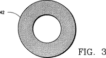
図3は、図2のスキャナで利用されているサンプル位置決め用の作用物の拡大図である。
図4は、図2のスキャナのピエゾチューブとスキャンフレームとの間に用いられるフレキシブル接続コネクタの略斜視図である。
好ましい実施形態の説明
本発明によれば、上記に概説した従来のピエゾスキャナにおける問題に対する解決策は、図1で示すようなピエゾチューブスキャナ10の能力を、平坦な結合構造内で利用することである。本発明にかかるフラットスキャナは、図2の符号12で概略的に示される。4つの同じ4分割スキャナ14、15、16及び17は、中央のステージのサンプル又はサンプルマウント20を支持するのに用いられ、そして走査を提供するのに利用される。各チューブ14〜17は、その一端が、対応する剛性コネクタ22〜25によって台座28に固定されていて、そして他端は、薄く、平坦で可撓性の4つのコネクタ32〜35の各々を介してスキャンフレーム30に取り付けられている。コネクタの平面を形成する二つの方向(X、Y)に応力がかかる場合にはコネクタは剛直であるが、それらの上面に対して垂線の方向(Z)には容易にたわむ。3つの小球38〜40が、スキャンフレーム30の上面に埋め込まれていて、さらに小球上に配置されるサンプルマウント20用のベースを提供する。選択的な付加物は、サンプルマウントを所定の位置に保持するためにスキャンフレーム上に配置された3つの小さなマグネット42である。
上記スキャナの重要な部品は、ピエゾチューブスキャナ14〜17をスキャンフレーム30に取り付けるフレキシブルコネクタ32〜34である。それらのコネクタの一つを、図2と同じ部品番号を付して図4に拡大している。
フレーム30の横方向(X−Y)の走査は、一対のピエゾチューブを用いて実行され、そしてXY面に垂直な方向(Z)における軸方向の位置決めは、4つのチューブ全てを同時に用いることで提供される。例えば、スキャンフレームを左に移動させる(図2を参照すると、X軸の負方向)ためには、チューブの左側及び右側の外側電極に適切な電圧を印加して、チューブ15、17を左に曲げる(図1参照)。チューブが曲がることで、コネクタ33は押され、コネクタ35は引かれることとなり、スキャンフレームに応力がかかる。コネクタ32、34は、応力のかかる方向に垂直になっていて、容易にたわむので、スキャンフレームは左に移動することができる。右への移動(X軸の正方向)は、チューブに印加する電圧を反対にして行う。Y方向への移動は、チューブ14、16に電圧を印加して、コネクタ33、35をわためることにより、独立して達成できる。
スキャンフレーム30の軸方向(Z方向)の移動は、4つ全てのチューブの上側電極と下側電極に同時に電圧を印加することで達成される。軸方向の移動範囲は横方向の移動範囲に等しく、かつ横方向の移動範囲とは完全に独立している。
装置の実際の走査範囲はピエゾチューブの固有の特性、チューブの寸法及び印加電圧に依存する。装置には8つの電気コネクタがあり、+X、−X、+Y、−Y、+Z、−Z、ピエゾ素子接地(ピエゾチューブの中心)、及びシャーシ接地から成っている。通常の走査電圧である+/−125Vで、商業的に入手できる直径0.125インチ、長さ1.25インチのチューブを用いて、走査範囲35μmのXYZスキャンを達成することができる。
サンプルの慣性移動は、前述の三脚型スキャナと同様に実行される。サンプルマウント20は、スキャンフレームに埋め込まれている3つの小球38、39及び40上に置かれる。サンプルマウントとフレームとの間の結合を強めて、逆さまの向きで操作を可能にすることが望まれる場合には、小さいマグネット42を含むことができる。サンプルを移動させるには、スキャンフレーム30を所望の方向に移動し、そして、サンプルマウントの慣性力によってサンプルマウントを所定の位置に維持し結果的にサンプルマウントの正味の変位を生じさせるのに十分な早さで、スキャンフレーム30を中立位置に戻す動作をする。
従来の結合構造と比較した本発明のスキャナの本質的な利点は、高倍率の顕微鏡の対物レンズの近くに容易に配置することができる平坦な薄いプレート内で、3次元走査が達成されることである。スキャナは、プレートの平面より下側に拡張されることがないので、対物レンズは、全ての光学顕微鏡で見られる簡単な回転機構によって、全く自由に交換できる。さらに、チューブ状ピエゾ素子を用い、軸方向の動きが横方向の領域の一部に制限される従来の3次元スキャナの構造とは違って、本発明の設計においては、軸方向の動きは横方向の動きと全く等しい。軸方向即ちZ方向の走査機構がチップを表面に容易に接触させることができるように、チップを表面に十分接近して従来の光学機器に配置するのが容易であるので、接近機構が非常に簡素になる。
もちろん、この走査技術は、それ自体が全ての走査用途において大いに役立つ。しかしながら、特に走査型プローブ顕微鏡が、この走査機構を装置に導入することによる利益を享受するであろう。これらの顕微鏡の全てにおいて、チップとサンプルとを同時に観察することは常に困難であったが、本発明の構造によってその制限は除かれる。このような顕微鏡では、プローブ及びその関連機構部を保持している第2のプレート50(透視状態で示されている)と、光学機器と、電子機器とがスキャンステージ30上に配置されて、共焦点スキャン光学顕微鏡を含む従来の光学顕微鏡の全種類と完全に互換性のある組込型の走査型プローブ顕微鏡システムを提供する。走査型プローブ顕微鏡の中でも、近視野の光学顕微鏡がこの設計による利益を最も享受するであろう。このような光学技術においては、従来の光学顕微鏡に優秀な3次元スキャナを完全に組み込むことは、光の観測及び光の収集のどちらにおいても絶対不可欠である。このことが、従来の光学顕微鏡と超解像度の近視野光学技術との間の視野を重ねることを可能にしている。このスキャナは、光学切片を得るために、現行では複雑な機構のレンズスキャンを用いてレンズの焦点面を変えている共焦点顕微鏡にも役立つであろう。
本発明は、好ましい実施形態に関して記載してきたが、以下の請求の範囲に記載された本発明の真の趣旨及び範囲から逸脱することなく変更が可能なことは、当業者にとっては明瞭である。TECHNICAL FIELD OF THE INVENTION A new piezo scanner design incorporates scanning in the X, Y, and Z directions within a flat stage that is 7 mm or less in height. With this apparatus, in addition to an axial positioning allowance of 30 microns, a scan range of 30 microns or more can be obtained. The scan stage also provides inertial movement of the sample over a few millimeters. In particular, the flat design is particularly suitable for operation in conjunction with near-field scanning optical microscopes and other optical microscope technologies such as confocal optical microscopes.
Background Art The scanning stage is located at the heart of all scanning probe microscopes (SPMs) (Di Salid, “Scanning Force Microscopy”, Oxford University Press, New York). The precise movement required for an SPM device to move a sample or to move a special chip that functions as an image element requires angstrom accuracy over a few microns, and the use of piezoelectric material is critical. Yes. Since these piezoelectric materials expand or contract when an electric field is applied across the piezoelectric material, they are generally used for minute positioning of small parts.
Various scanning techniques using known piezoelectric materials have been developed, but in all the techniques described below, a chip / sample for observing the sample and in the case of light emission or light absorption studies In order to collect light from the interaction area, it has been particularly problematic to place a high magnification microscope objective lens directly below or above the sample.
Prior Art Situation In the first Scanning Tunneling Microscope (STM), movement in the X, Y and Z directions relied on three orthogonal piezo positioning devices (Di Salid, “Scanning Force Microscopy” Oxford) University Press, New York). This piezo positioning device was immediately replaced by a single tube scanner developed by Binning and Smith that provides XY scanning and Z positioning by a single element (Di Salid, “Scanning Force”). Microscopy, Oxford University Press, New York). This element is composed of a single piezo tube, and as shown in FIG. 1, the external electrode is divided into four equal quadrants in this piezo tube. A positive voltage applied to one quadrant causes tube length elongation on one side, and a negative voltage of equal magnitude applied to the opposing quadrant causes a corresponding quadrant contraction. The final result is a tube bend. This bend is significantly greater than the axial elongation of the tube. In all scanning probe microscopes, such tube scanners remain in any form. While it is possible to scan several microns with a short tube, it is possible to provide a scanning range of 75-100 microns or more with a long tube.
A further advance was the introduction of a tripod scanner by Bessock (Kay Bessok, Surface Science 181, 145 (1987)). This scanner design utilizes three identical quadrant tube scanners together, with the sample resting on top of those tubes. This scanner allows anyone to scan the sample in the usual way and has the attendant features that the inertial transfer technique can roughly position the sample over a very wide range. This horizontal inertial movement is accomplished by slowly bending the three tubes to one side in a single motion, followed by rapidly straightening the tubes back to their initial positions. As the tube moves back, the sample remains in its position due to inertia, so the net result is that the sample moves laterally. This movement is possible in both the X and Y directions and is limited only by the size of the sample itself. Actual bending of the tube is achieved simply by applying a sawtooth voltage to the piezo element. In addition to movement, rough axial positioning can also be achieved by placing an appropriate mount sample and utilizing inertial rotation.
The biggest disadvantage of these single tube and tripod tube designs is that they extend long in the axial direction of the scanner. The wide-scan tubes currently used in commercial STM and AFM systems can be extended to a few inches in length (Di Thalid, “Scanning Force Microscopy”, Oxford University Press, New York). This restriction means that all the inspection optical instruments are arranged on one side of the sample, and the opposite area is a single area of the scanning mechanism. In near-field scanning optical microscopes, this limitation is especially problematic when it is desired to place a high magnification microscope objective directly below or directly above the sample for sample observation and near-field emission collection. ("Near-field Scanning Optical Microscope", U.S. Pat. No. 4,917,462 issued April 17, 1990). A number of devised solutions have been devised to overcome this problem. One option was to scan the chip rather than the sample (A Lewis and Kay Liberman “Nature” 354, 214 (1991)). This is undesirable because it may cause image artifacts and destroys the axial symmetry of the optical system. Another option involves placing the objective lens entirely within a large diameter single tube or in the center of a tripod scanner. In any of these methods, it is difficult or impossible to change the objective lens. The last possibility is to cantilever the sample at the end of a tube scanner located near the objective lens, but this method can cause serious problems that are mechanically unstable. .
SUMMARY OF THE INVENTION The device described herein is ideal for the above problem by providing scanning in three orthogonal directions in a thin and flat package that can be miniaturized on the order of several millimeters in height. Provide a simple solution. The apparatus is also ideally suited for stage scanning confocal optical microscopes. The device's inherent positioning capability in the axial direction provides a mechanism for optically slicing the sample in the Z direction while scanning the sample through confocal.
As described above, the present invention is a method and apparatus for performing three-dimensional wide-range scanning in a flat structure that can be reduced in size by several millimeters in height.
[Brief description of the drawings]
The foregoing and further objects, features, and advantages of the invention will become apparent from the following detailed description of the preferred embodiments, taken in conjunction with the accompanying drawings. In the attached drawings,
FIG. 1 shows a single tube piezo scanner.
FIG. 2 is a schematic top view of a flat stage piezo scanner according to the present invention.
FIG. 3 is an enlarged view of a sample positioning agent used in the scanner of FIG.
4 is a schematic perspective view of a flexible connector used between the piezo tube and the scan frame of the scanner of FIG.
DESCRIPTION OF THE PREFERRED EMBODIMENTS According to the present invention, the solution to the problems in the conventional piezo scanner outlined above is to utilize the capabilities of the
The important parts of the scanner are
The lateral (XY) scan of the
Movement of the
The actual scan range of the device depends on the inherent characteristics of the piezotube, the dimensions of the tube and the applied voltage. There are eight electrical connectors in the device, consisting of + X, -X, + Y, -Y, + Z, -Z, piezo element ground (piezotube center), and chassis ground. An XYZ scan with a scan range of 35 μm can be achieved using commercially available tubes with a diameter of 0.125 inches and a length of 1.25 inches at a normal scan voltage of +/− 125V.
The inertial movement of the sample is performed in the same manner as the above tripod scanner. The
The essential advantage of the scanner of the present invention compared to a conventional coupling structure is that three-dimensional scanning is achieved in a flat thin plate that can be easily placed near the objective lens of a high magnification microscope. It is. Since the scanner is not extended below the plane of the plate, the objective lens can be replaced quite freely by a simple rotation mechanism found in all optical microscopes. Furthermore, unlike conventional 3D scanner structures that use a tubular piezo element and the axial movement is limited to a portion of the lateral region, in the design of the present invention, the axial movement is lateral. It is exactly the same as the direction movement. Since the scanning mechanism in the axial or Z-direction can easily bring the chip into contact with the surface, it is easy to place the chip sufficiently close to the surface on a conventional optical instrument, so the access mechanism is very Be simple.
Of course, this scanning technique itself is very useful in all scanning applications. However, scanning probe microscopes in particular will benefit from the introduction of this scanning mechanism into the apparatus. In all of these microscopes, it has always been difficult to observe the tip and the sample at the same time, but the structure of the present invention removes that limitation. In such a microscope, a second plate 50 (shown in a transparent state) holding a probe and its related mechanism part, an optical instrument, and an electronic instrument are arranged on the
While the invention has been described in terms of a preferred embodiment, it will be apparent to those skilled in the art that modifications may be made without departing from the true spirit and scope of the invention as set forth in the claims below.
Claims (15)
スキャンフレームと、
4つの四分割筒状ピエゾ素子と、
複数の接続ジョイントと、を含むスキャンステージであって、
上記ピエゾ素子は、上記スキャンフレームと同一平面にあって、上記フレームを支持するために上記台座に接続されており、
ピエゾ素子は、上記スキャンフレームと間隔を隔てており、
各ピエゾ素子が隣接する素子に対して垂直であり、
各ピエゾ素子が第1の端部と第2の端部とを有しており、
各ピエゾ素子の上記第1の端部が上記台座に固定されており、
上記接続ジョイントが、上記ピエゾ素子の動作中において上記スキャンフレームの面内では軸方向に剛体で且つ横方向に可撓性であり、
上記接続ジョイントは、各ピエゾ素子の上記第2の端部と上記スキャンフレームとの間に接続されており、それによって上記ピエゾ素子の屈曲が、上記スキャンフレームに上記台座に対して直交方向の走査を提供するスキャンステージ。A pedestal,
A scan frame;
Four quadrant cylindrical piezo elements;
A scanning stage including a plurality of connecting joints,
The piezo element is flush with the scan frame and connected to the pedestal to support the frame;
The piezo element is spaced from the scan frame,
Each piezo element is perpendicular to the adjacent element;
Each piezo element has a first end and a second end;
The first end of each piezo element is fixed to the pedestal;
The connection joint is rigid in the axial direction and flexible in the lateral direction in the plane of the scan frame during operation of the piezo element;
The connection joint is connected between the second end of each piezo element and the scan frame, so that the bending of the piezo element causes the scan frame to scan in a direction perpendicular to the pedestal. Provide scanning stage.
Applications Claiming Priority (3)
| Application Number | Priority Date | Filing Date | Title |
|---|---|---|---|
| US08/564,018 US5705878A (en) | 1995-11-29 | 1995-11-29 | Flat scanning stage for scanned probe microscopy |
| US08/564,018 | 1995-11-29 | ||
| PCT/US1996/018553 WO1997020354A1 (en) | 1995-11-29 | 1996-11-27 | Flat scanning stage for scanned probe microscopy |
Publications (3)
| Publication Number | Publication Date |
|---|---|
| JP2000501500A JP2000501500A (en) | 2000-02-08 |
| JP2000501500A5 JP2000501500A5 (en) | 2004-10-21 |
| JP4014054B2 true JP4014054B2 (en) | 2007-11-28 |
Family
ID=24252839
Family Applications (1)
| Application Number | Title | Priority Date | Filing Date |
|---|---|---|---|
| JP52054597A Expired - Lifetime JP4014054B2 (en) | 1995-11-29 | 1996-11-27 | Flat scanning stage for scanning probe microscopes |
Country Status (5)
| Country | Link |
|---|---|
| US (1) | US5705878A (en) |
| EP (1) | EP0864181B1 (en) |
| JP (1) | JP4014054B2 (en) |
| DE (1) | DE69632691T2 (en) |
| WO (1) | WO1997020354A1 (en) |
Families Citing this family (35)
| Publication number | Priority date | Publication date | Assignee | Title |
|---|---|---|---|---|
| US6359370B1 (en) * | 1995-02-28 | 2002-03-19 | New Jersey Institute Of Technology | Piezoelectric multiple degree of freedom actuator |
| JPH10105243A (en) * | 1996-09-10 | 1998-04-24 | Hewlett Packard Co <Hp> | Positioning feature, positioning device and information recorder |
| AT410718B (en) * | 1998-10-28 | 2003-07-25 | Schindler Hansgeorg Dr | DEVICE FOR VISUALIZING MOLECULES |
| EP1316055A4 (en) | 2000-05-29 | 2006-10-04 | Vkb Inc | Virtual data entry device and method for input of alphanumeric and other data |
| US6787773B1 (en) | 2000-06-07 | 2004-09-07 | Kla-Tencor Corporation | Film thickness measurement using electron-beam induced x-ray microanalysis |
| GB2369489B (en) * | 2000-11-23 | 2004-03-10 | Khaled Karrai | Inertial rotation device |
| US6801596B2 (en) * | 2001-10-01 | 2004-10-05 | Kla-Tencor Technologies Corporation | Methods and apparatus for void characterization |
| EP1438754B1 (en) * | 2001-10-22 | 2005-12-28 | miniswys SA | Piezoelectric motor |
| US6798120B1 (en) * | 2001-10-31 | 2004-09-28 | The Regents Of The University Of California | Apparatus and method for manipulation of an object |
| US6810105B2 (en) * | 2002-01-25 | 2004-10-26 | Kla-Tencor Technologies Corporation | Methods and apparatus for dishing and erosion characterization |
| GB2385196B (en) * | 2002-02-11 | 2005-08-17 | 1 Ltd | Amplified actuator |
| US6888289B2 (en) * | 2002-07-16 | 2005-05-03 | Baldor Electric Company | Multi-axes, sub-micron positioner |
| US7687767B2 (en) * | 2002-12-20 | 2010-03-30 | Agilent Technologies, Inc. | Fast scanning stage for a scanning probe microscope |
| US7180662B2 (en) * | 2004-04-12 | 2007-02-20 | Applied Scientific Instrumentation Inc. | Stage assembly and method for optical microscope including Z-axis stage and piezoelectric actuator for rectilinear translation of Z stage |
| WO2006090386A2 (en) * | 2005-02-24 | 2006-08-31 | Vkb Inc. | A virtual keyboard device |
| WO2006119792A1 (en) * | 2005-05-12 | 2006-11-16 | Physik Instrumente (Pi) Gmbh & Co. Kg | Miniaturized biaxial piezo actuating device |
| JP2008546315A (en) * | 2005-05-31 | 2008-12-18 | ユニゾン・プロダクツ・インコーポレーテッド | Optimized piezoelectric design for mechanical-acoustic transducers |
| CN101288014A (en) * | 2005-10-17 | 2008-10-15 | 皇家飞利浦电子股份有限公司 | In-plane manipulator |
| JP2007158276A (en) * | 2005-12-08 | 2007-06-21 | Ngk Insulators Ltd | Piezo/electrostriction device, and method for driving same |
| JP2007228782A (en) * | 2006-01-24 | 2007-09-06 | Ngk Insulators Ltd | Piezoelectric/electrostrictive device |
| JP4448099B2 (en) * | 2006-02-01 | 2010-04-07 | キヤノン株式会社 | Scanning probe device |
| WO2008126236A1 (en) * | 2007-03-30 | 2008-10-23 | Pioneer Corporation | Driver |
| DE102007023217B4 (en) * | 2007-05-18 | 2011-07-21 | Continental Automotive GmbH, 30165 | Electromechanical motor, in particular piezoelectric micro-stepper drive |
| US20100322455A1 (en) * | 2007-11-21 | 2010-12-23 | Emo Labs, Inc. | Wireless loudspeaker |
| JP5197101B2 (en) * | 2008-03-31 | 2013-05-15 | 日本トムソン株式会社 | Movable table device |
| JP5722231B2 (en) * | 2008-12-18 | 2015-05-20 | ディスカバリー テクノロジー インターナショナル,インク. | Piezoelectric quasi-resonant motor based on acoustic standing wave with combined resonator |
| US8189851B2 (en) | 2009-03-06 | 2012-05-29 | Emo Labs, Inc. | Optically clear diaphragm for an acoustic transducer and method for making same |
| US20110044476A1 (en) * | 2009-08-14 | 2011-02-24 | Emo Labs, Inc. | System to generate electrical signals for a loudspeaker |
| CN103293339A (en) * | 2012-02-28 | 2013-09-11 | 中国科学院合肥物质科学研究院 | Combined piezoelectric tube scanner formed by double nested piezoelectric tube scanners for scanning together |
| EP2969264A4 (en) | 2013-03-15 | 2016-11-23 | Emo Labs Inc | Acoustic transducers with bend limiting member |
| USD741835S1 (en) | 2013-12-27 | 2015-10-27 | Emo Labs, Inc. | Speaker |
| USD733678S1 (en) | 2013-12-27 | 2015-07-07 | Emo Labs, Inc. | Audio speaker |
| USD748072S1 (en) | 2014-03-14 | 2016-01-26 | Emo Labs, Inc. | Sound bar audio speaker |
| CN103990998B (en) * | 2014-05-20 | 2017-01-25 | 广东工业大学 | Stiffness frequency adjustable two-dimensional micro-motion platform based on stress stiffening principle |
| US10263173B2 (en) * | 2015-01-16 | 2019-04-16 | The Regents Of The University Of Michigan | Multi-axis piezoelectric transducer |
Family Cites Families (18)
| Publication number | Priority date | Publication date | Assignee | Title |
|---|---|---|---|---|
| SU497551A1 (en) * | 1973-06-26 | 1975-12-30 | Московский институт электронной техники | Device for orientation |
| US4087715A (en) * | 1976-11-18 | 1978-05-02 | Hughes Aircraft Company | Piezoelectric electromechanical micropositioner |
| US4525852A (en) * | 1983-03-15 | 1985-06-25 | Micronix Partners | Alignment apparatus |
| US4523120A (en) * | 1984-06-04 | 1985-06-11 | The United States Of America As Represented By The Secretary Of The Navy | Precise bearing support ditherer with piezoelectric drive means |
| US4686440A (en) * | 1985-03-11 | 1987-08-11 | Yotaro Hatamura | Fine positioning device |
| DE3610540A1 (en) * | 1986-03-27 | 1987-10-01 | Kernforschungsanlage Juelich | MOTION DEVICE FOR MICROMOVING OBJECTS |
| US4678955A (en) * | 1986-04-18 | 1987-07-07 | Rca Corporation | Piezoelectric positioning device |
| JPS63262066A (en) * | 1987-04-20 | 1988-10-28 | Hitachi Ltd | Finely positioning device |
| US4917462A (en) * | 1988-06-15 | 1990-04-17 | Cornell Research Foundation, Inc. | Near field scanning optical microscopy |
| US5323082A (en) * | 1989-05-03 | 1994-06-21 | Spectra Physics Lasers, Inc. | Piezoelectric actuator for planar alignment |
| US5079471A (en) * | 1990-06-04 | 1992-01-07 | Martin Marietta Corporation | High torque harmonic traction motor |
| JPH04259015A (en) * | 1991-02-13 | 1992-09-14 | Canon Inc | Fine driving device |
| DE69203280T2 (en) * | 1991-04-29 | 1996-03-07 | Philips Electronics Nv | Displacement device. |
| US5173605A (en) * | 1991-05-02 | 1992-12-22 | Wyko Corporation | Compact temperature-compensated tube-type scanning probe with large scan range and independent x, y, and z control |
| US5281884A (en) * | 1992-06-03 | 1994-01-25 | At&T Bell Laboratories | Adjustable X-Y stage |
| US5306919A (en) * | 1992-09-21 | 1994-04-26 | Digital Instruments, Inc. | Positioning device for scanning probe microscopes |
| US5332942A (en) * | 1993-06-07 | 1994-07-26 | Rennex Brian G | Inchworm actuator |
| JPH07111143A (en) * | 1993-08-18 | 1995-04-25 | Jeol Ltd | Slit device |
-
1995
- 1995-11-29 US US08/564,018 patent/US5705878A/en not_active Expired - Lifetime
-
1996
- 1996-11-27 DE DE69632691T patent/DE69632691T2/en not_active Expired - Lifetime
- 1996-11-27 WO PCT/US1996/018553 patent/WO1997020354A1/en active IP Right Grant
- 1996-11-27 JP JP52054597A patent/JP4014054B2/en not_active Expired - Lifetime
- 1996-11-27 EP EP96940813A patent/EP0864181B1/en not_active Expired - Lifetime
Also Published As
| Publication number | Publication date |
|---|---|
| EP0864181A4 (en) | 2000-08-02 |
| US5705878A (en) | 1998-01-06 |
| EP0864181B1 (en) | 2004-06-09 |
| EP0864181A1 (en) | 1998-09-16 |
| DE69632691D1 (en) | 2004-07-15 |
| JP2000501500A (en) | 2000-02-08 |
| WO1997020354A1 (en) | 1997-06-05 |
| DE69632691T2 (en) | 2005-06-09 |
Similar Documents
| Publication | Publication Date | Title |
|---|---|---|
| JP4014054B2 (en) | Flat scanning stage for scanning probe microscopes | |
| JP4797150B2 (en) | Scanning mechanism and mechanical scanning microscope using the same | |
| US6861649B2 (en) | Balanced momentum probe holder | |
| WO1994025888A1 (en) | Optically guided macroscopic-scan-range/nanometer resolution probing system | |
| CN108780222B (en) | 3D MEMS scanner for real-time cross-section endomicroscopy | |
| JP3577141B2 (en) | Probe scanning mechanism and scanning probe microscope using the same | |
| Tsunemi et al. | Development of multi-environment dual-probe atomic force microscopy system using optical beam deflection sensors with vertically incident laser beams | |
| JP2003315239A (en) | Scanner for spm | |
| JPH1123584A (en) | Three-dimensional microscanning device | |
| CN101221116B (en) | Plate type three-dimensional locating/scanning device | |
| Cao et al. | Real-time vertical/horizontal section imaging and 3D image construction using a 3-axis electromagnetic confocal microscanner | |
| JPH0244787A (en) | Mechanism for aligning minute position of piezoelectric element | |
| JPH07181030A (en) | Interatomic force microscope | |
| Lee et al. | Versatile low-temperature atomic force microscope with in situ piezomotor controls, charge-coupled device vision, and tip-gated transport measurement capability | |
| Cai et al. | An alternative flat scanner and micropositioning method for scanning probe microscope | |
| JP6846056B2 (en) | Scanner and scanning probe microscope | |
| JPH0835972A (en) | Simplified spm apparatus | |
| JPH02147804A (en) | Scanning tunnel electron microscope | |
| Li et al. | Aerosol jet printed PZT actuated MEMS resonating cantilever scanner | |
| Marchman et al. | Optically guided large‐nanostructure probe | |
| JPH0868799A (en) | Scanning type probe microscope | |
| JPH10339735A (en) | Scanning type probe microscope | |
| JPH0743604Y2 (en) | Piezoelectric element micro positioning mechanism | |
| JPH05264212A (en) | Scanning tunneling microscope | |
| JPH0544723Y2 (en) |
Legal Events
| Date | Code | Title | Description |
|---|---|---|---|
| A521 | Request for written amendment filed |
Free format text: JAPANESE INTERMEDIATE CODE: A523 Effective date: 20031127 |
|
| A621 | Written request for application examination |
Free format text: JAPANESE INTERMEDIATE CODE: A621 Effective date: 20031127 |
|
| A131 | Notification of reasons for refusal |
Free format text: JAPANESE INTERMEDIATE CODE: A131 Effective date: 20061114 |
|
| A601 | Written request for extension of time |
Free format text: JAPANESE INTERMEDIATE CODE: A601 Effective date: 20070214 |
|
| A602 | Written permission of extension of time |
Free format text: JAPANESE INTERMEDIATE CODE: A602 Effective date: 20070402 |
|
| A521 | Request for written amendment filed |
Free format text: JAPANESE INTERMEDIATE CODE: A523 Effective date: 20070514 |
|
| A524 | Written submission of copy of amendment under article 19 pct |
Free format text: JAPANESE INTERMEDIATE CODE: A524 Effective date: 20070514 |
|
| TRDD | Decision of grant or rejection written | ||
| A01 | Written decision to grant a patent or to grant a registration (utility model) |
Free format text: JAPANESE INTERMEDIATE CODE: A01 Effective date: 20070807 |
|
| A61 | First payment of annual fees (during grant procedure) |
Free format text: JAPANESE INTERMEDIATE CODE: A61 Effective date: 20070906 |
|
| FPAY | Renewal fee payment (event date is renewal date of database) |
Free format text: PAYMENT UNTIL: 20100921 Year of fee payment: 3 |
|
| R150 | Certificate of patent or registration of utility model |
Free format text: JAPANESE INTERMEDIATE CODE: R150 |
|
| FPAY | Renewal fee payment (event date is renewal date of database) |
Free format text: PAYMENT UNTIL: 20110921 Year of fee payment: 4 |
|
| FPAY | Renewal fee payment (event date is renewal date of database) |
Free format text: PAYMENT UNTIL: 20120921 Year of fee payment: 5 |