JP4004302B2 - Image sensor - Google Patents
Image sensor Download PDFInfo
- Publication number
- JP4004302B2 JP4004302B2 JP2002031320A JP2002031320A JP4004302B2 JP 4004302 B2 JP4004302 B2 JP 4004302B2 JP 2002031320 A JP2002031320 A JP 2002031320A JP 2002031320 A JP2002031320 A JP 2002031320A JP 4004302 B2 JP4004302 B2 JP 4004302B2
- Authority
- JP
- Japan
- Prior art keywords
- pixel region
- light receiving
- light
- receiving element
- peripheral portion
- Prior art date
- Legal status (The legal status is an assumption and is not a legal conclusion. Google has not performed a legal analysis and makes no representation as to the accuracy of the status listed.)
- Expired - Fee Related
Links
Images


Landscapes
- Solid State Image Pick-Up Elements (AREA)
- Transforming Light Signals Into Electric Signals (AREA)
Description
【0001】
【発明の属する技術分野】
本発明は、被写体光を光電的に取り込むことで被写体画像を得る撮像素子に関する。
【0002】
【従来の技術】
近年急速に普及しているデジタルカメラやビデオカメラの本体内には、被写体光を光電信号に変換して画像を記録するCCDイメージセンサ(以下CCDと略記する)などの撮像素子が組み込まれている。このような撮像素子は、被写体光を受光して光電信号に変換する受光素子と、この受光素子上に形成された色フィルタと、受光素子への集光率を向上させるために色フィルタ上に配置されたマイクロレンズとから構成される画素が、マトリクス状に複数配置された画素領域を備えている。
【0003】
上記のような撮像素子には、画素領域の中央部に比べて周辺部の信号出力が減衰するシェーディングという現象が発生する。このシェーディングは、周辺部へ入射光が斜めに入射して光電変換効率が悪化することに起因する。シェーディングが発生すると、画素領域の中央部と周辺部で画像のバランスが悪くなって全体的に不自然な画像となるため、製品の性能を著しく低下させる。
【0004】
この問題を解決する手段として、特開平10−125887号公報や特開2001−160973号公報には、マイクロレンズを受光素子に対して画素領域の中央方向に一定間隔でシフトさせて配置することで、画素領域の周辺部における光電変換効率を改善させてシェーディングを補正する方法が記載されている。
【0005】
【発明が解決しようとする課題】
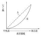
しかしながら、特開平10−125887号公報や特開2001−160973号公報に記載の方法は、マイクロレンズのシフト量が画素領域の中央部から周辺部に向かって線形的に変化するため(図3のA参照)、例えこのシフト量が最適化されたとしても、周辺部近辺での光量の減衰が大となり(図4のC参照)、全体的に均整のとれた画像を得ることができないという欠点があった。
【0006】
本発明は、画素領域の周辺部近辺での光量の減衰によるシェーディングの影響を少なくすることで、全体的に均整のとれた画像を得ることができる撮像素子を提供することを目的とする。
【0007】
【課題を解決するための手段】
上記目的を達成するために、本発明は、被写体光を受光して光電信号に変換する受光素子と、この受光素子上に形成された色フィルタと、前記受光素子への集光率を向上させるために前記色フィルタ上に配置されたマイクロレンズとから構成される画素が、マトリクス状に複数配置された画素領域を備えた撮像素子において、前記マイクロレンズは、前記受光素子に対して前記画素領域の中央方向にシフトして配置され、前記マイクロレンズと前記受光素子とのシフト量は、前記画素領域の中央部から周辺部に向かって非線形的に変化することを特徴とする。なお、前記シフト量は、前記画素領域の中央部では小さく、前記画素領域の周辺部に向かうにつれて大となることが好ましい。
【0008】
【発明の実施の形態】
図1に、本発明を実施した撮像素子の断面図を示す。撮像素子2は、基板3、受光素子4、第1保護膜5、色フィルタ6、第2保護膜7、マイクロレンズ8から構成される。基板3は、シリコンウエハなどの半導体からなり、この基板3上に受光素子4が配置される。各受光素子4上には、第1保護膜5を介して色フィルタ6が配置される。この色フィルタ6は、例えばRGB3色のフィルタが図2に示すように各受光素子4上に配列され、これによりカラー画像を得る。また、集光率を向上させるためにマイクロレンズ8が第2保護膜7上に配置される。これらの受光素子4、色フィルタ6、およびマイクロレンズ8などにより、1つの画素9(図中2点鎖線で囲む部分)が構成され、この画素9がマトリクス状に複数配置されて画素領域10が形成される。
【0009】
マイクロレンズ8は、受光素子4に対して画素領域10の中央方向にシフトして配置される。マイクロレンズ8と受光素子4とのシフト量11は、図3のBで示すように、画素領域10の中央部から周辺部に向かって非線形的に変化する。このシフト量11は、画素領域10の中央部では小さく、画素領域10の周辺部に向かうにつれて指数関数的に大となっている。
【0010】
周辺部におけるシフト量11は、受光素子4に対する被写体光の入射効率が最大となるように設定され、中央部と周辺部との間のシェーディングが補正される。一方、中央部におけるシフト量11は、受光素子4に対する被写体光の入射効率が若干減少するように設定されている。これにより、画素領域10の周辺部近辺での光量の減衰によるシェーディングの影響が少なくなる。
【0011】
上記構成による撮像素子2の画素領域10における光量分布は、図4のDで示すように、周辺部近辺での光量の減衰が小となる。すなわち、画素領域10の中央部から周辺部に向かって光量がなだらかに減衰している。したがって、画素領域の周辺部近辺でのシェーディングの影響を少なくすることができる。
【0012】
以上、図示した実施形態にしたがって説明してきたが、撮像素子としては、CCDを用いたものでも、MOS型デバイスを用いたものでもよい。また、色フィルタの配列は、図2に示すように、RGB3色による原色系の構成でもよいし、シアン、イエロー、マゼンタの補色系による構成でもよく、これらを組み合わせて構成されるものでもよい。
【0013】
なお、上記実施形態では、マイクロレンズのシフト量を、画素領域の周辺部に向かうにつれて指数関数的に大となるように設定したが、画素領域の周辺部近辺でのシェーディングの影響が少なくなればよく、例えば図3のBで示される曲線に沿って階段状に変化させてもよい。また、このシフト量を各色フィルタ毎に設定して色シェーディングを補正してもよい。
【0014】
【発明の効果】
以上のように、本発明の撮像素子によれば、マイクロレンズが受光素子に対して画素領域の中央方向にシフトして配置され、マイクロレンズと受光素子とのシフト量が、画素領域の中央部から周辺部に向かって非線形的に変化するので、全体的に均整のとれた画像を得ることが可能である。
【図面の簡単な説明】
【図1】本発明を実施した撮像素子の断面図である。
【図2】色フィルタの配列の一例を示す図である。
【図3】画素領域におけるマイクロレンズのシフト量の変化を示すグラフである。
【図4】画素領域における光量の変化を示すグラフである。
【符号の説明】
2 撮像素子
4 受光素子
6 色フィルタ
8 マイクロレンズ
9 画素
10 画素領域
11 シフト量[0001]
BACKGROUND OF THE INVENTION
The present invention relates to an imaging element that obtains a subject image by photoelectrically capturing subject light.
[0002]
[Prior art]
An image sensor such as a CCD image sensor (hereinafter abbreviated as CCD) that records an image by converting subject light into a photoelectric signal is incorporated in the body of a digital camera or video camera that has been rapidly spreading in recent years. . Such an image sensor includes a light receiving element that receives subject light and converts it into a photoelectric signal, a color filter formed on the light receiving element, and a color filter to improve a light collection rate on the light receiving element. A plurality of pixels each composed of the arranged microlenses has a pixel region arranged in a matrix.
[0003]
In the imaging device as described above, a phenomenon called shading occurs in which the signal output in the peripheral portion is attenuated as compared with the central portion of the pixel region. This shading is caused by incident light incident on the peripheral portion obliquely and deterioration of photoelectric conversion efficiency. When shading occurs, the balance between images at the central and peripheral portions of the pixel area becomes poor, resulting in an unnatural image as a whole, which significantly degrades the performance of the product.
[0004]
As means for solving this problem, Japanese Patent Application Laid-Open Nos. 10-125877 and 2001-160973 disclose that microlenses are arranged by being shifted at regular intervals in the center direction of the pixel region with respect to the light receiving element. A method for correcting shading by improving the photoelectric conversion efficiency in the peripheral portion of the pixel region is described.
[0005]
[Problems to be solved by the invention]
However, the methods described in Japanese Patent Application Laid-Open Nos. 10-12587 and 2001-160973 linearly change the shift amount of the microlens from the central part to the peripheral part of the pixel region (see FIG. 3). Even if this shift amount is optimized, the attenuation of the amount of light in the vicinity of the peripheral portion becomes large (see C in FIG. 4), and it is impossible to obtain a generally balanced image. was there.
[0006]
It is an object of the present invention to provide an image sensor that can obtain an overall well-balanced image by reducing the influence of shading due to the attenuation of the amount of light near the periphery of a pixel region.
[0007]
[Means for Solving the Problems]
In order to achieve the above object, the present invention improves a light receiving element that receives subject light and converts it into a photoelectric signal, a color filter formed on the light receiving element, and a light collection rate on the light receiving element. Therefore, in the image pickup device including a pixel region in which a plurality of pixels each including a microlens arranged on the color filter are arranged in a matrix, the microlens has the pixel region with respect to the light receiving device. The amount of shift between the microlens and the light receiving element varies nonlinearly from the center to the periphery of the pixel region. The shift amount is preferably small in the central portion of the pixel region and becomes larger toward the peripheral portion of the pixel region.
[0008]
DETAILED DESCRIPTION OF THE INVENTION
FIG. 1 shows a cross-sectional view of an imaging device embodying the present invention. The imaging element 2 includes a
[0009]
The microlens 8 is arranged with a shift in the center direction of the pixel region 10 with respect to the light receiving element 4. The shift amount 11 between the microlens 8 and the light receiving element 4 changes nonlinearly from the central portion of the pixel region 10 toward the peripheral portion, as indicated by B in FIG. This shift amount 11 is small at the center of the pixel region 10 and increases exponentially as it goes to the periphery of the pixel region 10.
[0010]
The shift amount 11 in the peripheral portion is set so that the incident efficiency of the subject light with respect to the light receiving element 4 is maximized, and shading between the central portion and the peripheral portion is corrected. On the other hand, the shift amount 11 at the center is set so that the incident efficiency of the subject light with respect to the light receiving element 4 is slightly reduced. As a result, the influence of shading due to the attenuation of the amount of light near the periphery of the pixel region 10 is reduced.
[0011]
In the light amount distribution in the pixel region 10 of the image pickup device 2 having the above configuration, the attenuation of the light amount in the vicinity of the peripheral portion is small as indicated by D in FIG. That is, the amount of light gradually attenuates from the central portion of the pixel region 10 toward the peripheral portion. Therefore, the influence of shading near the periphery of the pixel region can be reduced.
[0012]
As described above, the description has been given according to the illustrated embodiment. However, the image sensor may be a CCD or a MOS device. Further, as shown in FIG. 2, the arrangement of the color filters may be a primary color system configuration of RGB, a cyan, yellow, and magenta complementary color system, or a combination thereof.
[0013]
In the above embodiment, the shift amount of the microlens is set so as to increase exponentially as it goes to the periphery of the pixel region. However, if the influence of shading near the periphery of the pixel region is reduced, For example, it may be changed stepwise along the curve indicated by B in FIG. Further, the color shading may be corrected by setting this shift amount for each color filter.
[0014]
【The invention's effect】
As described above, according to the imaging element of the present invention, the microlens is arranged to be shifted in the center direction of the pixel area with respect to the light receiving element, and the shift amount between the microlens and the light receiving element is set at the center of the pixel area. Therefore, it is possible to obtain a generally well-balanced image.
[Brief description of the drawings]
FIG. 1 is a cross-sectional view of an image sensor embodying the present invention.
FIG. 2 is a diagram illustrating an example of an arrangement of color filters.
FIG. 3 is a graph showing changes in the shift amount of a microlens in a pixel region.
FIG. 4 is a graph showing a change in light amount in a pixel region.
[Explanation of symbols]
2 Image sensor 4 Light receiving element 6 Color filter 8 Micro lens 9 Pixel 10 Pixel area 11 Shift amount
Claims (2)
前記マイクロレンズは、前記受光素子に対して前記画素領域の中央方向にシフトして配置され、前記周辺部の光量の落ち込みが目立たないように、前記画素領域の周辺部における前記マイクロレンズと前記受光素子とのシフト量は、前記周辺部の入射効率が最大となるように設定され、前記画素領域の中央部と周辺部の間の前記シフト量は、前記中央部と周辺部の間の入射効率が減少するように設定されていることを特徴とする撮像素子。A light receiving element that receives subject light and converts it into a photoelectric signal, a color filter formed on the light receiving element, and a microlens disposed on the color filter to improve a light collection rate on the light receiving element In an imaging device having a pixel region in which a plurality of pixels configured by
The microlens is arranged so as to be shifted in the center direction of the pixel region with respect to the light receiving element, and the light reception of the microlens and the light receiving portion in the peripheral portion of the pixel region is conspicuous so that the amount of light in the peripheral portion is not conspicuous. The shift amount with respect to the element is set so that the incident efficiency of the peripheral portion is maximized, and the shift amount between the central portion and the peripheral portion of the pixel region is the incident efficiency between the central portion and the peripheral portion. An image pickup device that is set so as to decrease.
Priority Applications (1)
| Application Number | Priority Date | Filing Date | Title |
|---|---|---|---|
| JP2002031320A JP4004302B2 (en) | 2002-02-07 | 2002-02-07 | Image sensor |
Applications Claiming Priority (1)
| Application Number | Priority Date | Filing Date | Title |
|---|---|---|---|
| JP2002031320A JP4004302B2 (en) | 2002-02-07 | 2002-02-07 | Image sensor |
Publications (2)
| Publication Number | Publication Date |
|---|---|
| JP2003234965A JP2003234965A (en) | 2003-08-22 |
| JP4004302B2 true JP4004302B2 (en) | 2007-11-07 |
Family
ID=27774762
Family Applications (1)
| Application Number | Title | Priority Date | Filing Date |
|---|---|---|---|
| JP2002031320A Expired - Fee Related JP4004302B2 (en) | 2002-02-07 | 2002-02-07 | Image sensor |
Country Status (1)
| Country | Link |
|---|---|
| JP (1) | JP4004302B2 (en) |
Cited By (1)
| Publication number | Priority date | Publication date | Assignee | Title |
|---|---|---|---|---|
| US9947708B2 (en) | 2015-02-13 | 2018-04-17 | Renesas Electronics Corporation | Semiconductor device and manufacturing method of the same |
Families Citing this family (6)
| Publication number | Priority date | Publication date | Assignee | Title |
|---|---|---|---|---|
| DE102004003013B3 (en) * | 2004-01-20 | 2005-06-02 | Fraunhofer-Gesellschaft zur Förderung der angewandten Forschung e.V. | Optical imaging system for timepiece, portable computer, mobile telephone, spectacles, clothing item, chip card or sticker using array of optical channels with relatively angled optical axes |
| JP4224789B2 (en) | 2004-03-01 | 2009-02-18 | ソニー株式会社 | Imaging device |
| JP4728660B2 (en) * | 2005-02-23 | 2011-07-20 | 株式会社東芝 | Solid-state imaging device and camera device using the same |
| JP4844513B2 (en) * | 2007-09-10 | 2011-12-28 | 大日本印刷株式会社 | Solid-state imaging device and imaging apparatus using the same |
| JP4998227B2 (en) * | 2007-11-22 | 2012-08-15 | 大日本印刷株式会社 | SOLID-STATE IMAGING ELEMENT, MANUFACTURING METHOD THEREOF, AND IMAGING DEVICE USING THIS SOLID-STATE IMAGING ELEMENT |
| JP5272433B2 (en) * | 2008-02-15 | 2013-08-28 | 富士通セミコンダクター株式会社 | Method and apparatus for calculating shift amount of image pickup device, image pickup device, and device incorporating image pickup device |
-
2002
- 2002-02-07 JP JP2002031320A patent/JP4004302B2/en not_active Expired - Fee Related
Cited By (1)
| Publication number | Priority date | Publication date | Assignee | Title |
|---|---|---|---|---|
| US9947708B2 (en) | 2015-02-13 | 2018-04-17 | Renesas Electronics Corporation | Semiconductor device and manufacturing method of the same |
Also Published As
| Publication number | Publication date |
|---|---|
| JP2003234965A (en) | 2003-08-22 |
Similar Documents
| Publication | Publication Date | Title |
|---|---|---|
| JP3981034B2 (en) | Color image acquisition device and color electronic camera | |
| WO2022088311A1 (en) | Image processing method, camera assembly and mobile terminal | |
| US8339489B2 (en) | Image photographing apparatus, method and medium with stack-type image sensor, complementary color filter, and white filter | |
| JP5442571B2 (en) | Solid-state imaging device and imaging device | |
| US7928352B2 (en) | Solid-state image capturing device, image capturing device, and manufacturing method of solid-state image capturing device | |
| JP4536072B2 (en) | Imaging device | |
| US8780253B2 (en) | Solid-state imaging device and signal processing circuit | |
| US8018516B2 (en) | Solid-state image sensor and signal processing method of same | |
| TW200816805A (en) | Solid-state image sensor | |
| JP2007311447A (en) | Photoelectric converter | |
| KR20070115243A (en) | Apparatus for photographing image and operating method for the same | |
| JP2009017544A (en) | Image pickup device | |
| WO2018198766A1 (en) | Solid-state image capturing device and electronic instrument | |
| JP2007288549A (en) | Physical information acquiring method and device thereof | |
| US20220336508A1 (en) | Image sensor, camera assembly and mobile terminal | |
| JP4512504B2 (en) | Microlens mounted single-plate color solid-state imaging device and image input device | |
| JP4579043B2 (en) | Solid-state imaging device and imaging apparatus | |
| JP4004302B2 (en) | Image sensor | |
| JP2001210812A (en) | Solid-state image pickup device and solid-state image pickup system provided with the same | |
| JP3920683B2 (en) | Image sensor | |
| JP2007066962A (en) | Color solid-state imaging device and digital camera | |
| JP4902106B2 (en) | Solid-state imaging device and digital camera | |
| JP2005347475A (en) | Solid state image sensor and solid state imaging system | |
| JP2006202907A (en) | Image pickup element | |
| JP2003243639A (en) | Image pickup element and image pickup device |
Legal Events
| Date | Code | Title | Description |
|---|---|---|---|
| A621 | Written request for application examination |
Free format text: JAPANESE INTERMEDIATE CODE: A621 Effective date: 20040311 |
|
| A977 | Report on retrieval |
Free format text: JAPANESE INTERMEDIATE CODE: A971007 Effective date: 20060928 |
|
| A131 | Notification of reasons for refusal |
Free format text: JAPANESE INTERMEDIATE CODE: A131 Effective date: 20061003 |
|
| A521 | Request for written amendment filed |
Free format text: JAPANESE INTERMEDIATE CODE: A523 Effective date: 20061130 |
|
| A711 | Notification of change in applicant |
Free format text: JAPANESE INTERMEDIATE CODE: A712 Effective date: 20061205 |
|
| A131 | Notification of reasons for refusal |
Free format text: JAPANESE INTERMEDIATE CODE: A131 Effective date: 20070530 |
|
| A521 | Request for written amendment filed |
Free format text: JAPANESE INTERMEDIATE CODE: A523 Effective date: 20070713 |
|
| TRDD | Decision of grant or rejection written | ||
| A01 | Written decision to grant a patent or to grant a registration (utility model) |
Free format text: JAPANESE INTERMEDIATE CODE: A01 Effective date: 20070815 |
|
| A61 | First payment of annual fees (during grant procedure) |
Free format text: JAPANESE INTERMEDIATE CODE: A61 Effective date: 20070821 |
|
| R150 | Certificate of patent or registration of utility model |
Ref document number: 4004302 Country of ref document: JP Free format text: JAPANESE INTERMEDIATE CODE: R150 Free format text: JAPANESE INTERMEDIATE CODE: R150 |
|
| FPAY | Renewal fee payment (event date is renewal date of database) |
Free format text: PAYMENT UNTIL: 20100831 Year of fee payment: 3 |
|
| FPAY | Renewal fee payment (event date is renewal date of database) |
Free format text: PAYMENT UNTIL: 20110831 Year of fee payment: 4 |
|
| R250 | Receipt of annual fees |
Free format text: JAPANESE INTERMEDIATE CODE: R250 |
|
| FPAY | Renewal fee payment (event date is renewal date of database) |
Free format text: PAYMENT UNTIL: 20110831 Year of fee payment: 4 |
|
| FPAY | Renewal fee payment (event date is renewal date of database) |
Free format text: PAYMENT UNTIL: 20120831 Year of fee payment: 5 |
|
| R250 | Receipt of annual fees |
Free format text: JAPANESE INTERMEDIATE CODE: R250 |
|
| FPAY | Renewal fee payment (event date is renewal date of database) |
Free format text: PAYMENT UNTIL: 20120831 Year of fee payment: 5 |
|
| FPAY | Renewal fee payment (event date is renewal date of database) |
Free format text: PAYMENT UNTIL: 20130831 Year of fee payment: 6 |
|
| R250 | Receipt of annual fees |
Free format text: JAPANESE INTERMEDIATE CODE: R250 |
|
| R250 | Receipt of annual fees |
Free format text: JAPANESE INTERMEDIATE CODE: R250 |
|
| R250 | Receipt of annual fees |
Free format text: JAPANESE INTERMEDIATE CODE: R250 |
|
| R250 | Receipt of annual fees |
Free format text: JAPANESE INTERMEDIATE CODE: R250 |
|
| R250 | Receipt of annual fees |
Free format text: JAPANESE INTERMEDIATE CODE: R250 |
|
| R250 | Receipt of annual fees |
Free format text: JAPANESE INTERMEDIATE CODE: R250 |
|
| R250 | Receipt of annual fees |
Free format text: JAPANESE INTERMEDIATE CODE: R250 |
|
| R250 | Receipt of annual fees |
Free format text: JAPANESE INTERMEDIATE CODE: R250 |
|
| R250 | Receipt of annual fees |
Free format text: JAPANESE INTERMEDIATE CODE: R250 |
|
| LAPS | Cancellation because of no payment of annual fees |