JP4001663B2 - Logic selection circuit - Google Patents
Logic selection circuit Download PDFInfo
- Publication number
- JP4001663B2 JP4001663B2 JP22879797A JP22879797A JP4001663B2 JP 4001663 B2 JP4001663 B2 JP 4001663B2 JP 22879797 A JP22879797 A JP 22879797A JP 22879797 A JP22879797 A JP 22879797A JP 4001663 B2 JP4001663 B2 JP 4001663B2
- Authority
- JP
- Japan
- Prior art keywords
- circuit
- interconnect
- selection circuit
- logic selection
- logic
- Prior art date
- Legal status (The legal status is an assumption and is not a legal conclusion. Google has not performed a legal analysis and makes no representation as to the accuracy of the status listed.)
- Expired - Lifetime
Links
Images
Classifications
-
- G—PHYSICS
- G05—CONTROLLING; REGULATING
- G05B—CONTROL OR REGULATING SYSTEMS IN GENERAL; FUNCTIONAL ELEMENTS OF SUCH SYSTEMS; MONITORING OR TESTING ARRANGEMENTS FOR SUCH SYSTEMS OR ELEMENTS
- G05B19/00—Program-control systems
- G05B19/02—Program-control systems electric
- G05B19/04—Program control other than numerical control, i.e. in sequence controllers or logic controllers
- G05B19/042—Program control other than numerical control, i.e. in sequence controllers or logic controllers using digital processors
- G05B19/0423—Input/output
Landscapes
- Physics & Mathematics (AREA)
- General Physics & Mathematics (AREA)
- Engineering & Computer Science (AREA)
- Automation & Control Theory (AREA)
- Electronic Switches (AREA)
- Logic Circuits (AREA)
Description
【0001】
【発明の属する技術分野】
本発明は、全体として、改良に係る論理回路、より具体的には、望ましくない人的介入を必要とせずに、電子回路を相互に接続し得るようにトランジスタ論理型式を自動的に適合させる論理選択回路に関する。一つの好適な適用例において、この論理選択回路は、磁気近接センサの出力端子とプログラム化可能な論理コントローラの対応する入力端子との間にてトランジスタ論理型式を自動的に適合させる。この適用例において、この磁気近接センサは、例えば、ロッドレスシリンダのようなシリンダ内で典型的に見られる可動のピストンと空間的な関係に配置された、例えば、磁石から生ずる磁界を検出する。磁気近接センサの回路と電気的に結合された論理選択回路は、磁気近接センサ及びプログラム化可能な論理コントローラが電気的に互いに適正に連通することを確実にする。
【0002】
【従来の技術】
2つ以上の電子回路間の相互接続部を形成し得る構造とされた各種型式の論理回路がある。当該技術分野にて周知であるように、バイポーラ型トランジスタ技術は、NPNトランジスタ及びPNPトランジスタという2つの基本的なトランジスタ論理型式から成っている。NPNトランジスタは「受信型(sinking)」トランジスタとして公知である一方、PNPトランジスタは「送信型(sourcing)」トランジスタとして公知である。
【0003】
【発明が解決しようとする課題】
電子回路が通信相互接続するためには、そのトランジスタ論理型式が適正に適合することを必要とし、さもなければ、回路は互いに適正に連通し得ない。従来、相互接続する電子回路間にてトランジスタ論理型式を適正に適合させるためには、人的介入が必要とされていた。その典型的な状況において、その相互接続部自体がその両論理型式のトランジスタを有しており、相互接続回路をその適合するトランジスタ論理型式と手操作にて接続することを必要とする。電子システム及び回路網のスケールは不断に増大するため、この人的介入によるコストは著しく多額となっている。更に、意図せずに人的な誤りを犯すならば、故障修理費用も多額となる。
【0004】
従来技術のトランジスタ論理型式を適合させる回路を使用することは、ある適用例においては満足し得る結果が得られるものの、上述した人的介入に伴う時間、誤り、及び費用を避けることはできなかった。
【0005】
本発明は、電子回路を相互接続すべく適合するトランジスタ論理型式を自動的に選択する論理選択回路を提供することにより、従来技術のトランジスタ論理型式の適合回路の上記の欠点及びその他の欠点を解消するものである。
【0006】
本発明の論理選択回路を利用する一つの重要な目的は、トランスデューサの出力端子と、相互接続するデータ取得システムの対応する入力端子との間に適正に適合した相互接続部を形成することである。このトランデューサは、ある種の外的刺激に対して電気的に応答することのできる任意の要素を備えることができる。この要素は、ソレノイド、センサ、リレー、近接スイッチ、押釦、又はキーボードを含むが、これらにのみ限定されるものではない。このトランスデューサは、該トランスデューサの相互接続端子と、データ取得システムとの間に適正に適合した相互接続部が形成されることを確実にすべく、本発明の論理選択回路を更に備えることが可能である。一つの代替的な実施の形態において、この論理選択回路は、トランスデューサ回路の実装体の外部に設けることができるが、これにも拘わらず、この回路が相互接続部として機能することを可能にするような方法にて、トランスデューサ及びデータ取得システムに接続することも可能である。
【0007】
当該出願のデータ取得システムは、殆どの任意の処理装置を備えることができる。かかる処理装置には、トランスデューサにより伝送された信号を受け取り且つその受け取った信号に応答して機械、又はその他の電子回路を制御する、プログラム化可能な論理コントローラ、又はトランスデューサにより伝送された信号を受け取り且つ所定のユーザが設定した命令に従ってその信号を更に処理し、又は記憶する、コンピュータ端子さえも含まれるが、これにのみ限定されるものではない。
【0008】
本発明の論理選択回路の使用について、特定の語及び特定の実施の形態に関して以下に説明する。この特定の語、及び特定の実施の形態は、例えば、ロッドレスシリンダのようなシリンダ内の可動ピストンの動きを制御する装置に関するものである。特に、シリンダの両端に植え込まれた各磁気近接センサ内にこの論理選択回路が組み込まれる。その磁気近接センサの各々は、近傍の磁界が存在するか否かを検出する。上述の説明において、磁界は、ピストンに関して空間的関係に配置された永久磁石から生ずる。こうした永久磁石の1つが磁気近接センサに接近したとき(即ち、ピストンがそのセンサに近接する位置にきたとき)、センサの出口端子には、所定の電圧レベルが存在する。他方、この永久磁石が磁気近接センサに接近する位置にないとき(即ち、可動ピストンがセンサに近接する位置にないとき)、センサの出力端子には、異なる大きさの所定の電圧レベルが存在する。
【0009】
【課題を解決するための手段】
磁気近接センサの各々が永久磁石から生ずる近傍の磁界が存在することを検出したならば、そのセンサは、該センサと電気的に結合されたプログラム化可能な論理コントローラに信号を送る。この論理選択回路の目的は、全ての状況下にて、相互接続する磁気近接センサの入口端子により送られたこの信号をプログラム化可能な論理コントローラの対応する入力端子が的確に識別し得るようにすることである。
【0010】
特に、磁気近接センサの各々に見られる論理選択回路は、その磁気近接センサの各々の出力端子と、相互接続するプログラム化可能な論理コントローラの対応する出力端子との間に適正に適合したトランジスタ論理型式が存在することを確実にする。この結果を得るため、そのコントローラが識別可能である電圧レベルが比較的高電圧レベル又は比較的低電圧レベルであるか否かに対応して、既にプログラム化可能な論理コントローラの対応する入力端子に存在する電圧レベルをこの論理選択回路が「受信」し、又は「発信」する。通常の環境下にて、その端子における電圧信号レベルがその前に比較的高電圧レベルにあったとき、そのプログラム化可能な論理コントローラの対応する入力端子に存在する電圧レベルをその論理選択回路が「受信」する(即ち、接地する)。これと逆に、その端子における電圧信号のレベルがその前に比較的低電圧レベルにあったとき、その論理選択回路は、プログラム化可能な論理コントローラの対応する入力端子に電流を「発信」し、これにより、その入力端子にある電圧信号を比較的高電圧レベルまで励起する。その何れの場合にも、プログラム化可能な論理コントローラの入力端子にある電圧レベルはその前の電圧レベルと反対にされる。従って、このプログラム化可能な論理コントローラは、磁気近接センサの各々が近傍の磁界を検出したことを識別することができる。
【0011】
本明細書は、上記意義の本発明の論理選択回路について説明するが、本発明は、その他の最終用途の環境にて具体化するのにも十分、適している。例えば、本発明の論理選択回路を気象制御システムに利用することも可能である。この適用例において、温度センサが典型的に包み込んだ部屋内の温度を監視し、その温度が所定の値に達したとき、制御装置に対しイネーブル信号を伝送する。次に、この制御装置は、該温度センサから受け取った信号に応答して空調装置、又は暖房装置を制御する。本発明の論理選択回路がないならば、この制御装置の入力端子は温度センサの対応する出力端子から伝送された信号を識別することができず、これら2つの装置の相互接続する端子のトランジスタ論理型式が既に適正に適合された状態とはならない。
【0012】
また、本発明の論理選択回路は、交通監視システムにて具体化することも可能である。特に、この論理選択回路は、自動車の交通を識別する、近接スイッチの出力端子と、通過する自動車に応答して近接スイッチにより伝送された信号を処理する制御装置の対応する入力端子との間の相互接続部として機能する。この制御装置は、例えば、1日当たり特定の時間単位にて識別された交通パターンに関する情報を記憶させることもできる。これとは代替的に、この制御装置は、効率的な交通管制を行うため、交通信号装置の作動を制御することもできる。この場合にも、本発明の論理選択回路を使用しなければ、この制御装置の入力端子は近接スイッチの対応する出力端子から伝送された信号を識別することができず、これらそれぞれの装置の相互接続する端子のトランジスタ論理型式が既に適正に適合している状況とはならない。
【0013】
上記の適用例は、何れの手段によっても、本発明の論理選択回路を利用する可能な適用例の全てを網羅するものではない。こうした適用例は、本発明の論理選択回路の使用が望ましい多数の適用例の幾つかを単に摘出したものに過ぎない。
【0014】
本発明は、従来技術に優る顕著な利点を提供する。本発明以前、技術者は、トランスデューサの出力端子のトランジスタ論理型式がデータ取得システムの対応する入力端子のトランジスタ論理型式と適正に適合させることが必要とされていた。さもなければ、トランスデューサ及びデータ取得システムを互いに適正に連通せず、それらはが組み合わせときに実質的に使用不能である。トランスデューサの出力端子とデータ取得システムの対応する入力端子との間にて適正に適合したトランジスタ論理型式を必要とするこの条件を満足させるため、技術者は、適正に適合した相互接続面を形成する設計とされた対応するトランジスタに対してトランスデューサ及びデータ取得システムの双方を手で接続する必要がある。
【0015】
本発明の論理選択回路によれば、この作業は最早、不要となる。特に、本発明の論理選択回路は、共に周知のトランジスタ論理型式であるトランジスタを含む。この論理選択回路は、相互接続する電子回路間に適正に適合した相互接続面を形成するのに必要とされる、相互接続するトランジスタを自動的に選択する。上記の適用例において、この論理選択回路は、トランスデューサとデータ取得システムとの間の相互接続面を適正に適合させ、これにより、その2つの相互接続回路は、互いに適正に連通することを確実にする。
【0016】
従って、本発明の全体的な目的は、相互接続する電子回路に対しトランジスタ論理型式を適合させる新規な方法を提供することである。
【0017】
本発明のより具体的な目的は、電子回路を相互接続するため、トランジスタ論理型式を適合させるのに従来必要とされた、コスト高で且つ誤りを犯し易い人的介入が不要の論理選択回路を提供することである。
【0018】
本発明のより具体的な目的は、電子回路を相互接続すべく、トランジスタ論理型式を自動的に適合させる論理選択回路を提供することである。
【0019】
本発明の更に具体的な目的は、データ取得システム及びトランスデューサの双方と電気的に結合された論理選択回路であって、その双方の回路間にてトランジスタ論理型式を自動的に適合させ、その回路が電気的に連通する状態にて互いに適正に連通することを確実にする、上記の論理選択回路を提供することである。
【0020】
本発明の更に具体的な目的は、プログラム化可能な論理コントローラ及び磁気近接センサの双方と電気的に結合され、そのセンサが、典型的にシリンダ内に配置される型式の可動ピストンと空間的な関係に配置された永久磁石が存在するか否かに応答し得る設計とされた論理選択回路を提供することである。
【0021】
第一の相互接続回路のトランジスタの論理型式を第二の相互接続回路のトランジスタの論理型式と選択的に適合させ、これにより、その2つの相互接続回路を電気的に互いに適正に連通し得るようにする論理選択回路が提供される。この論理選択回路は、第一の相互接続回路に接続可能である制御相互接続線と、第二の相互接続回路に接続可能である中央相互接続線と、2つの相互接続回路のトランジスタ論理型式に選択的に適合する回路適合化手段と、制御接続線にイネーブル信号が存在する間に、入力側における存在する電圧信号を回路適合化手段にラッチする回路ラッチ手段とから成っている。
【0022】
【発明の実施の形態】
新規であると考えられる本発明の特徴は、具体的に、特許請求の範囲に記載されている。本発明は、同様の構成要素は同様の参照符号で示す、幾つかの添付図面と共に以下の説明を参照することにより、その更なる目的及び利点と共に、最も良く理解することができる。
【0023】
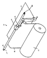
図1を参照すると、全体として、参照符号10で表示した切断装置は、ロッドレスシリンダ12と、キャリッジ14と、切断要素16と、可動ピストン17(図2)と、材料19のロール18と、一連のローラ20とを備える状態で示してある。図面には、ロッドレスシリンダが図示されているが、説明する実施の形態にて、一般的なシリンダ(即ち、ロッドレスでないシリンダ)を使用することが可能であることが理解されよう。しかしながら、一貫性を保つため、シリンダ12は、ロッドレスシリンダとして説明する。
【0024】
作動時、材料19のウェブ21は、図示するような方法にて一連のローラを通じて供給され、その材料ウェブは切断要素16に近接する位置に配置される。キャリッジ14に取り付けられた切断要素16を使用して所望の位置にて材料のウェブを切断する。材料を切断するため、切断要素16は、可動ピストン17の動きにより長手方向に向けて材料のウェブを横断するように引きずる。この可動ピストンは、切断要素と作用可能に関係付けられており、また、ロッドレスシリンダ12内に配置されている。可動ピストン17及び切断要素16は、当該技術分野で周知の任意の方法にて互いに作用可能に関係付けることが可能であることが理解されよう。図1に図示した特定の実施の形態において、キャリッジ14は、例えば、可動ピストン17と磁気に結合させ、ピストンがロッドレスシリンダ12内で何れかの軸方向に動くとき、切断要素が同一方向に動くようにすることができる。この磁気結合部の強度によりキャリッジ14が作用中に支承可能な荷重が決まる。上述した適用例において、キャリッジ14は、ロッドレスシリンダ12の開始端22から開始して材料を切断しつつ、ロッドレスシリンダの仕上げ端24に向けて移動し、所望の切断が完了した後に、その開始端に戻る。
【0025】
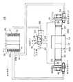
次に、図2を参照すると、キャリッジ14の移動及び復帰は、典型的に、全体として参照符号25で示した、電子制御型の空圧装置により行われる。プログラム化可能な論理コントローラ26は、2位置(4ウェイ)弁27と電気的に連通しており、この2位置弁27は、その内部に、ソレノイド28と、2位置部材29と、ばね部材30とを備えている。この2位置部材29の位置は、プログラム化可能な論理コントローラ26により制御される。
【0026】
特に、プログラム化可能な論理コントローラ26がその出力端子31、32に電圧を付与すると、2位置弁27内のソレノイド28が励起される。このソレノイド28の励起により磁界が生じ、この磁界は、ばね部材30の中立のばね力に打ち勝って、2位置弁をして2位置部材29を図2に図示しない位置に変位させる。この変位位置にて、弁の供給通路33がロッドレスシリンダ12の開始端22と連通しており、また、該弁の放出通路34がロッドレスシリンダ12の仕上げ端24と連通する。
【0027】
他方、プログラム化可能な論理コントローラ26がその出力端31、32に電圧を付与しないとき、ソレノイド28は非励起状態にある。この状況のとき、ばね部材30の中立のばねは、2位置弁27をして2位置部材29を図2に図示した位置に変位させる。この変位位置にて、供給通路33がロッドレスシリンダ12の仕上げ端24と連通し、放出通路34がロッドレスシリンダ12の開始端22と連通する。
【0028】
作動時、このように2位置弁27が2位置部材29を変位させることで、キャリッジ14の移動及び復帰動作が制御される。具体的には、可動ピストン17、従ってキャリッジ14は、最初、ロッドレスシリンダ12の開始端22にて静止している。プログラム化可能な論理コントローラ26が外部の発信源(図示せず)からの命令信号を待つ。この信号は空気圧装置25に命令して、キャリッジ14を開始端22から仕上げ端24まで移動させる。プログラム化可能な論理コントローラ26の入力端子35にてこの命令信号を受け取ったとき、コントローラは、その出力端子31、32に電圧を付与し、これらの出力端子は、上述したように供給通路33及び放出通路34をそれぞれ開始端22及び仕上げ端24と連通させる。その結果、全体として参照符号36で示した円筒状容積内の空気圧力は上昇し始め、全体として参照符号37で示した円筒状容積内の空気圧力は低下し始める。定義として、円筒状容積36は、開始端22と可動ピストン17とによりその境が設定されたロッドレスシリンダ12内の容積である。更に、定義として、円筒状容積37は、仕上げ端24と可動ピストン17とによりその境が設定されたロッドレスシリンダ12内の容積である。
【0029】
円筒状容積36内の空気圧が円筒状容積37内の空気圧を上廻ったならば、可動ピストン17に差圧の力が付与されて、該可動ピストンをロッドレスシリンダ12の仕上げ端24に向けて移動させる。キャリッジ14は、可動ピストン17と磁性的に結合されているため、当該キャリッジも同一方向に移動する。更に、該キャリッジ14に取り付けられた切断要素16(図1参照)も同一方向に移動する。従って、切断装置10は、所望の位置にて材料19のウェブ21を切断することができる(図1参照)。
【0030】
上述した実施の形態において、該仕上げ端24に近接する位置に配置された磁気近接スイッチ38が第一の永久磁石38a(キャリッジ14の一端に取り付けられた磁石)から生じる磁界が存在するか否かを検出する迄、該キャリッジ14は、ロッドレスシリンダ12の仕上げ端24に向けて動く。磁気近接センサ38がこの磁界が存在することを検出したならば、その回路内に本発明の論理選択回路を含むセンサが、プログラム化可能な論理コントローラ26の入力端子40、41に存在する電圧信号のレベルを変化させる。特に、このセンサは、入力端子40、41に存在するトランジスタの論理型式に依存して、その信号のレベルを比較的高電圧レベルから比較的低電圧レベルへと変化させる。
【0031】
プログラム化可能な論理コントローラ26の入力端子40、41における電圧レベルが磁気近接センサ38により変化されると、該コントローラは、その出力端子31、32に予め付与された電圧を除去する。このソレノイド28の励起停止により、上述したように、供給通路33及び放出通路34は、それぞれ仕上げ端24及び開始端22と連通する。その結果、円筒状容積36内の空気圧力が低下し始め、円筒状容積37内の空気圧力は上昇し始める。
【0032】
円筒状容積37内の空気圧力が円筒状容積36内の空気圧力を上廻ったならば、可動ピストン17に差圧力が付与されて、該ピストンは、ロッドレスシリンダ12の開始端22に向けて復帰する。該キャリッジ14は、可動ピストン17と磁気的に結合されているため、そのキャリッジも同一方向に向けて移動する。磁気近接センサ38と同様の設計及び作用を有するようにすることができる磁気近接センサ42が第一の永久磁石38aの反対側のキャリッジ14の端部に取り付けられた第二の永久磁石42aから生じる近傍の磁界が存在するか否かを検出する迄、このキャリッジは、ロッドレスシリンダ12の開始端22に向けて復帰を続ける。この磁界の存在を検出したならば、同様にその回路内に本発明の論理選択回路を含む磁気近接センサ42は、プログラム化可能な論理コントローラ26の入力端子43a、43bに信号を伝送し、空圧装置26が外部の発信源(図示せず)から後続の命令信号を受け取る用意が整っていることを示す。この場合にも、センサ42は、こうした端子に存在するトランジスタの論理型式に依存して、端子43a、43bにおける電圧信号レベルを比較的高電圧レベルから比較的低電圧レベルへと変化させる。
【0033】
本発明は、回路、即ち、磁気近接センサ38の回路と電気的に結合された論理選択回路に関するものである。更に、第一の論理選択回路と設計及び作用の点で同一である第二の論理選択回路を磁気近接センサ42の回路と電気的に結合させることができる。こうした論理選択回路の目的は、磁気近接センサ38、42の出力端子とプログラム化可能な論理コントローラ26の対応する入力端子40、41又は43a、43bとの間にてトランジスタの論理型式を適合させることである。本発明の回路は、図1及び図2の切断装置のキャリッジの制御に利用される磁気近接センサの各々に使用されるものとして説明したが、この回路は、各種の適用例にて利用可能であることが理解されよう。例えば、図1及び図2に図示したシリンダは、作業環境内の異なる位置の間にて材料を搬送し、また、機械内への材料の供給、扉の開放、更にシルクスクリーンとしてさえも使用が可能である。広義において、本発明の回路は、2つ以上の電子回路の任意の相互接続部に対して有利な結果が得られるような設計とされている。このため、本発明の回路は、全体として論理選択回路と称される。
【0034】
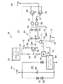
図3に図示した一つの好適な実施の形態に示すように、磁気近接センサ38(図2)は、全体として参照符号44で表示した論理選択回路を備えている。しかしながら、この論理選択回路44は、当該技術分野で周知の任意の方法にて磁気近接センサ38と電気的に結合可能であることが理解されよう。更に、磁気近接センサ42(図2)は、図3に図示した論理選択回路44と設計及び作用の点で同一である論理選択回路を含む。この場合にも、この論理選択回路は、当該技術分野で周知の任意の方法にて磁気近接センサ42と電気的に結合可能であることが理解されよう。簡略化の目的のため、この磁気近接センサ44の回路内の論理選択回路について本明細書では説明しない。しかしながら、この磁気近接センサ42の回路内のこの論理選択回路は、図3に関して以下に説明する論理選択回路44と同様の方法にて作用するものであることが理解されよう。
【0035】
図3に図示するように、論理選択回路44を含む磁気近接センサ38の回路は、本明細書において、プログラム化可能な論理コントローラ26として示したデータ取得システムと電気的に結合されている。該論理選択回路44は、論理選択回路とプログラム化可能な論理コントローラ26との間に完全に二重デジタル通信に対応することのできる通信相互接続部46を備えている。通信相互接続部46は抵抗器48の第一の端子に接続され、該抵抗器は、抵抗器50と組み合わされている間に、電圧分割器の上半体として機能する。抵抗器48、50の値は十分に大きくて、プログラム化可能な論理コントローラ26からの望ましくない漏洩電流を極く最小に保ち得るようにする。抵抗器48の第二の端子は、抵抗器50の第一の端子に、及び入力装置(この実施の形態において、NPNトランジスタ52として図示)の基部電極に接続される。同様に、抵抗器50の第一の端子は、NPNトランジスタ52の基部電極に接続される。しかしながら、この抵抗器の第二の端子は直接、接地接続され、これにより、電圧分割器の回路網を完成させる。抵抗器48、50は、共に作用して、NPNトランジスタ52の基部電極に電圧信号を付与する。この電圧信号は、通信相互接続部46(即ち、プログラム化可能な論理コントローラ26の入力端子)に存在する電圧レベルの所定の一部分を含む電圧レベルを有する。
【0036】
従来の受信又は一般的なエミッタの形態に従い、NPNトランジスタ52の集電電極は、プルアップ抵抗器56を通じて電源54に接続され、その装置のエミッタ電極は直接、接地接続されている。通信相互接続部46(即ち、プログラム化可能な論理コントローラ26の入力端子)に比較的高電圧の電圧信号が存在するとき、抵抗器48、50から成る電圧分割器回路網は、全体として高レベルの電圧信号をNPNトランジスタ52の基部電極に付与する。これに応答して、NPNトランジスタ52は、導電状態となり、その集電電極の電圧は接地レベル(以下、低電圧レベルと称する)まで低下する。他方、通信相互接続部46(即ち、プログラム化可能な論理コントローラ26の入力端子)に比較的低レベルの電圧信号が存在するとき、その電圧分割器回路網は、全体として低レベルの電圧信号をNPNトランジスタ52の基部電極に付与する。これに応答して、NPNトランジスタ52は非導電状態となり、その集電電極は、電源54の電圧レベル(以下、高電圧レベルと称する)に近似した電圧レベルとなる。従って、NPNトランジスタ52の集電電極の電圧は、高及び低として示した2つの略異なる電圧レベルとなることができ、このことは、NPNトランジスタが論理選択回路44に対する入力装置として機能することを可能にする。
【0037】
NPNトランジスタ52の集電電極は、従来通りの設計及び作用とすることのできる否定ゲート58の入力端子に更に接続されている。否定ゲート58の出力端子は、NPNトランジスタ52の集電電極に存在する電圧信号レベルの論理逆数である電圧レベルを有する。この逆の電圧信号は、次に、全体として参照符号62で示したデータラッチ(従来通りの設計及び作用とすることができる)のデータ入力線60に付与される。このため、NPNトランジスタ52の集電電極に存在する電圧信号が高レベルである場合、否定ゲート58はデータラッチ62のデータ入力線に低レベルの電圧信号を付与する。更に、NPNトランジスタ52の集電電極に存在する電圧信号が低レベルである場合、その否定ゲートはデータラッチ62のデータ入力線に高レベルの電圧信号を付与する。データラッチ62のデータ入力線は、通信相互接続部46(即ち、プログラム化可能な論理コントローラ26の入力端子)に存在する信号の電圧レベルが比較的高いとき、高電圧レベルとなることが理解されよう。同様にして、通信相互接続部46(即ち、プログラム化可能な論理コントローラ26の入力端子)に存在する信号の電圧レベルが比較的低いとき、データラッチ62のデータ入力線は、低電圧レベルとなる。このようにして、データラッチ62のデータ入力線60に存在する電圧レベルは、通信相互接続部46(即ち、プログラム化可能な論理コントローラ26の入力端子)に存在する信号の電圧レベルに従う。
【0038】
データ入力線60に加えて、データラッチ62は、クロック線64と、出力線66と、逆出力線68とを含む。クロック線64に存在する電圧信号が電圧レベルの変化を励起して変化させるときに限り、データラッチ62は、その従来のサンプルモードに入る。この電圧レベルの変化は、プラスのエッジ励起ラッチの場合は、低から高への変化であり、また、マイナスのエッジの励起データラッチの場合は、高から低への変化となる。この励起変化が生じると、データラッチ62はその変化を検出し、そのサンプルモードに入り、このサンプルモードにて、データラッチはデータ入力線60に存在する信号の電圧レベルを出力線66に伝送する。更に、該データラッチ62は、そのデータ入力線に存在する信号の電圧レベルを逆にし、この逆信号をその時点にて逆となった出力線68に伝送する。
【0039】
他方、データラッチ62のクロック線64がそのサンプルモードを励起させる変化を行わないとき、該ラッチは、その従来のラッチモードに止まり、このラッチモードにて、該ラッチはその出力線及びその逆出力線に存在する電圧信号をロックする。更に、このラッチは、そのラッチモードにある間に、そのデータ入力線に存在する電圧信号を最早、抽出することはない。
【0040】
データラッチ62のクロック線64は、ANDゲート70の出力端子からその電圧信号を受け取る。ANDゲート70の第一の入力端子71は、クロックパルス発生器72に接続されており、該クロックパルス発生器は、典型的に、当該技術分野で周知の方法にて交流の高電圧及び低電圧列を発生させる。このクロック72は、本発明の全ての回路のタイミング条件を満足させる当該技術分野で周知の型式の遅延機構を含むことができることが理解されよう。ANDゲート70の第二の入力端子73は、プルアップ抵抗器76を通じて電源74に接続され、また、否定ゲート78の入力端子、及び制御相互接続部79に接続される。該制御相互接続部は、論理選択回路44を通信励起回路80に接続する。この通信励起回路は、従来型式の設計の磁気近接スイッチとして図3に図示されている。特に、通信励起回路は、ソリッドステートのセンサ82と、電源84と、ショットキダイオード86と、コンデンサ88と、対向した2つのツェナダイオード90、92とから成る幾つかの回路構成要素を含んでいる。ソリッドステートセンサ82は3つの端子を有する。第一の端子は、ショットキダイオード86を通じて接続された電源84からセンサが必要とする作用電力を受け取る。第二の端子は、直接、接地接続され、第三の端子は、制御相互接続部79により論理選択回路44に接続されている。これにより、センサは、外的刺激を感知したとき、論理選択回路にイネーブル信号を伝送することができる。上述した適用例において、この外的刺激は、可動ピストン17がロッドレスシリンダ12の仕上げ端24にあるとき(図2参照)、永久磁石38aの近接スイッチから生じる近傍の磁界である。
【0041】
ショットキダイオード86、コンデンサ88、対向するツェナダイオード90、92は全て、ソリッドステータセンサ82の保護手段として機能する。特に、ショットキダイオード86は、センサの端子に逆極性が付与されるのを防止し、ショットキダイオード及びセンサの組み合体と並列に接続されたコンデンサ88は、電源84から誤って吸引される可能性のある全ての交流電圧からセンサを隔離し、また、ショットキダイオード及びセンサの組み合体と並列に接続された対向したツェナダイオード90、92は、センサに付与される最大電圧を制限する。
【0042】
通信励起回路80は、論理選択回路44に対する制御機構として機能する。特に、通信励起回路80が論理選択回路44にイネーブル信号を送らないとき(即ち、可動ピストン17がロッドレスシリンダ12の仕上げ端24から十分に離れ、ソリッドステートセンサ82が永久磁石38aから生じる近傍の磁界が存在することを検出しないとき(図2参照))、ANDゲート70の第二の入力端子73は、電源74の電圧レベルに近似した高電圧レベルとなり、このため、ゲートの出力端子は、クロック72から発生された交流のパルス列の電圧レベルに従う。こうした状況のとき、データラッチ62のクロック線64は、クロック72により駆動される。その結果、データラッチ62は、該クロックが交互に変化するときに一致して、そのサンプルモードに入り、データ入力線60に存在する電圧信号を抽出する。このデータ入力線は、上述したように、プログラム化可能な論理コントローラ26の入力端子に存在する電圧信号に従う。
【0043】
通信励起回路80が論理選択回路44にイネーブル信号を送るとき(即ち、可動ピストン17がロッドレスシリンダ12の仕上げ端24に十分に近接し、ソリッドステートセンサ82が、永久磁石38aから生ずる信号の磁界の存在を検出するとき(図2参照))、ANDゲート70の第二の入力端子73は、低電圧レベルとなる。これに応答して、ANDゲート70の出力端子、及び同様に、データラッチ62のクロック線64の双方が低電圧レベルとなる。こうした状況にて、クロック線64の励起は何ら変化しないため、データラッチ62は、そのラッチモードに止まり、最早、データ入力線60から抽出することはない。その代わり、このラッチは、その出力側及び逆出力線66、68に存在するそれぞれの電圧信号を保ち、通信励起回路80が論理選択回路44にイネーブル信号を再度、送ることができなくなるとき(即ち、可動ピストン17はロッドレスシリンダ12の仕上げ端24から十分に離れて、ソリッドステートセンサ82が永久磁石38aから生ずる近傍の磁界が存在することを検出しなくなるとき(図2参照))迄、その状態を保ち、これにより、ラッチを定期的に再度、そのサンプルモードに入れる。
【0044】
ラッチ62は、そのサンプルモードに定期的に入る一方、否定ゲート78への入力は、電源74の電圧に近似した高電圧レベルとなる。これに応答して、ANDゲート94の入力端子に接続された否定ゲート78の出力端子は、低電圧レベルとなる。このため、ANDゲート94の出力端子は、ゲートのその他の入力端子に存在する電圧信号のレベルに関係なく、低電圧レベルとなる。このANDゲート94の出力端子に存在するこの低電圧レベルは、NPNトランジスタ95の基部電極に付与されて、その装置を非導電性にする。
【0045】
ANDゲート94に加えて、否定ゲート78は、ANDゲート96の1つの入力端子に接続される。上述したように、ラッチ62は、定期的にそのサンプルモードに入る一方、否定ゲート78の出力端子、及び同様に、ANDゲート96の入力端子に低電圧レベルの信号が存在する。これに応答して、ANDゲート96の出力端子は、その他方の入力端子に存在する電圧信号のレベルに関係なく、定電圧レベルへと励起される。このANDゲートの出力端子は、否定ゲート97の入力端子に接続される。この場合、否定ゲート97の出力端子は、高電圧レベルとなり、この電圧レベルは、PNPトランジスタ98の基部電極に付与されて、その装置を非導電性にする。
【0046】
従って、通信励起回路80が論理選択回路44にイネーブル信号を送らないとき(即ち、可動ピストン17がロッドレスシリンダ12の仕上げ端24から十分に離れ、ソリッドステートセンサ82が永久磁石38aから生ずる近傍の磁界が存在することを検出しないとき(図2参照))、データラッチ62は、定期的にそのサンプルモードに入る。更に、NPNトランジスタ95及びPNPトランジスタ98の双方が非導電性とされる。
【0047】
データラッチ62がそのラッチモードに止まる、別の状況のとき、否定ゲート78への入力端子は低電圧レベルにあり、このゲートにより高電圧レベルに変換されて、次に、ANDゲート94の1つの入力端子に付与される。ANDゲート94の他方の入力端子は、データラッチ62の出力線66に接続される。このように、こうした状況にてANDゲート94の出力端子は、出力線66に存在する信号の電圧レベルに従い、その電圧レベルの信号をNPNトランジスタ95の基部電極に付与する。同様にして、否定ゲート78の出力端子はANDゲート96の1つの入力端子に接続される。ANDゲート96の他方の入力端子は、データラッチ62の逆の出力線68に接続される。
【0048】
このため、こうした状況下にて、ANDゲート96の出力端子は、逆の出力線68に存在する信号の電圧レベルに従い、その電圧レベルの信号を否定ゲート97の入力端子に付与する。このゲートがその信号の電圧レベルを逆にして、その逆の信号をPNPトランジスタ98の基部電極に伝送する。データラッチ62がそのラッチモードにある間、PNPトランジスタ98の基部電極に存在する電圧レベルは、NPNトランジスタ95の基部電極に存在する電圧信号レベルと等しいことが理解されよう。特に、通信励起回路80が論理選択回路44にイネーブル信号を送る前(即ち、可動ピストン17がロッドレスシリンダ12の仕上げ端24に十分に近接した位置に配置され、ソリッドステートセンサ82が永久磁石38aから生ずる近傍の磁界を検出する直前(図2参照))に、データ入力線60の第一のサンプルが、抽出されるとき、比較的高電圧レベルを有する信号が通信相互接続部46(即ち、プログラム化可能な論理コントローラ26の入力端子)に存在するならば、その双方トランジスタの基部電極は、高電圧レベルに設定される。同様に、データの入力線60の最後のサンプンが抽出されるとき(即ち、可動ピストン17がロッドレスシリンダ12の仕上げ端24に十分に近接した位置に配置され、ソリッドステートセンサ82が永久磁石38aから生ずる近傍の磁界を検出する直前(図2参照))に、比較的低電圧レベルを有する信号が通信相互接続部(即ち、プログラム化可能な論理コントローラ26の入力端子)に存在するならば、その双方トランジスタの基部電極は、低電圧レベルに設定される。
【0049】
従来の受信形態に従い、NPNトランジスタ95のエミッタ電極は、接地接続され、その集電電極は通信相互接続部46(即ち、プログラム化可能な論理コントローラ26の入力端子に)接続される。このため、データラッチ62がそのサンプルモードから出てそのラッチモードに入るとき(即ち、通信励起回路80が論理選択回路44にイネーブル信号を送り、ソリッドステートセンサ82が永久磁石38aから生ずる近傍の磁界を検出するとき(図2参照))、比較的高電圧レベルを有する信号が通信相互接続部(即ち、プログラム化可能な論理コントローラ26の入力端子)に存在するならば、NPNトランジスタ95の基部電極及び集電電極は、最初に、対応する高電圧レベルとなり、その結果、その装置が導電性とされる。次に、NPNトランジスタ95は、通信相互接続部(即ち、プログラム化可能な論理コントローラ26の入力端子)に存在する電圧信号のレベルを低下させ、接地又は低電圧レベルにする。この間、データラッチ62は、通信相互接続部(即ち、プログラム化可能な論理コントローラ26の入力端子)に存在する電圧信号が再度、高電圧レベルとなるのを防止している。他方、データラッチ62がそのサンプルモードから出て、そのラッチモードに入るとき、通信相互接続部(即ち、プログラム化可能な論理コントローラ26の入力端子)に比較的低電圧レベルの信号が存在するならば、そのラッチモードの時間中、対応する低電圧レベルの信号がその基部電極に付与されるから、NPNトランジスタ95は、非導電性とされる。こうした状況下にて、NPNトランジスタ95は、通信相互接続部(即ち、プログラム化可能な論理コントローラ26の入力端子)に存在する電圧信号のレベルに何ら影響を与えない。
【0050】
従来の発信形態に従い、PNPトランジスタ98のエミッタ電極は、電源99に直接、接続され、その集電電極は、通信相互接続部46(即ち、プログラム化可能な論理コントローラ26の入力端子)に接続される。このため、データラッチ62がそのサンプルモードから出て、そのラッチモードに入るとき(即ち、可動ピストン17がロッドレスシリンダ12の仕上げ端24に十分に近接する位置まで移動し、ソリッドステートセンサ82が永久磁石38aから生ずる近傍の磁界の存在を検出するとき(図2参照))、通信相互接続部(即ち、プログラム化可能な論理コントローラ26の入力端子)に比較的高電圧を有する信号が存在するならば、PNPトランジスタ98の基部電極は、そのラッチモード時間の全体に亙って、対応する高電圧レベルとなる。これにより、PNPトランジスタ98は非導電性とされ、このため、その装置は、通信相互接続部(即ち、プログラム化可能な論理コントローラ26の入力端子)に存在する電圧信号のレベルに何ら影響を与えない。しかしながら、データラッチ62がそのサンプルモードから出て、そのラッチモードに入るとき(即ち、可動ピストン17がロッドレスシリンダ12の仕上げ端24に十分に近接する位置まで移動し、ソリッドステートセンサ82が永久磁石38aから生ずる近傍の磁界の存在を検出するとき(図2参照))、通信相互接続部46(即ち、プログラム化可能な論理コントローラ26の入力端子)に比較的低電圧の信号が存在するならば、最初に、その基部電極及び集電電極に、低電圧レベルの対応する信号が付与されるため、PNPトランジスタ98は、導電性とされる。このPNPトランジスタ98の導電性により、電源99は通信相互接続部46に電流を発信し、その結果、該通信相互接続部は、電源99の電圧レベルと近似した高電圧レベルとなる。その結果、プログラム化可能な論理コントローラの入力端子も電源99の電圧レベルに近似した同一の高電圧レベルとなる。こうした状況下にて、データラッチ62は、通信相互接続部(即ち、プログラム化可能な論理コントローラ26の入力端子)が再度、低電圧レベルとなるのを防止する。
【0051】
従って、データラッチ62がそのサンプルモードから出て、そのラッチモードに入るとき(即ち、可動ピストン17がロッドレスシリンダ12の仕上げ端24に十分に近接する位置まで移動し、ソリッドステートセンサ82が永久磁石38aから生ずる近傍の磁界の存在を検出するとき(図2参照))、通信相互接続部46(即ち、プログラム化可能な論理コントローラ26の入力端子)に比較的高電圧を有する信号が存在するならば、ラッチがそのサンプルモードに再度入るとき(即ち、可動ピストン17がロッドレスシリンダ12の仕上げ端24から十分に離れる方向に動いて、ソリッドステートセンサが永久磁石38aから生ずる近傍の磁界の存在を最早、検出しなくなるとき(図2参照))迄、NPNトランジスタ95は、通信相互接続部(即ち、プログラム化可能な論理コントローラ26の入力端子)に存在する電圧信号のレベルを低下させる。他方、データラッチ62がそのサンプルモードから出て、そのラッチモードに入るとき(即ち、可動ピストン17がロッドレスシリンダ12の仕上げ端24に十分に近接するまで移動し、ソリッドステートセンサ82が永久磁石38aから生ずる近傍の磁界の存在を検出するとき(図2参照))、通信相互接続部46(即ち、プログラム化可能な論理コントローラ26の入力端子)に比較的高電圧を有する信号が存在するならば、PNPトランジスタ98は、電源99が通信相互接続部に電流を発信し、これにより、通信相互接続部(即ち、プログラム化可能な論理コントローラ26の入力端子)に存在する電圧信号を励起して、その電源の電圧のレベルに近似した高レベルにする。データラッチ62が再度、そのサンプルモードに入ったとき(即ち、可動ピストン17がロッドレスシリンダ12の仕上げ端24から十分に離れる程度に移動し、ソリッドステートセンサが最早、永久磁石38aから生ずる磁界の存在を検出し得ないとき(図2参照))、NPNトランジスタ95及びPNPトランジスタ98の双方が非導電状態となり、これにより、通信相互接続部46(即ち、プログラム化可能な論理コントローラ26の入力端子)がその通常の作用電圧レベルとなることを可能にする。
【0052】
本発明の一つの特定の実施の形態を図示し且つ説明したが、その広い形態にて本発明から逸脱せずに、その変更及び改変例が具体化可能であることが当業者に明らかであろうし、このため、特許請求の範囲の目的は、本発明の真の精神及び範囲に属するかかる全ての変更及び改変例を包含することである。
【図面の簡単な説明】
【図1】本発明の論理回路を利用することのできる多数の適用例の1つの示す、切断装置の斜視図である。
【図2】図1に図示した切断装置の制御に使用される電子的に制御される空圧装置の概略図である。
【図3】本発明に従って形成された論理選択回路を含む、図2に図示した電子的に制御される空圧装置の磁気近接センサの1つとプログラム化可能な論理コントローラの間の電気的な概略図である。
【符号の説明】
10 切断装置 12 ロッドレスシリンダ
14 キャリッジ 16 切断要素
17 可動ピストン 18 ロール
19 材料 20 ローラ
21 材料のウェブ 22 ロッドレスシリンダの開始端
24 ロッドレスシリンダの仕上げ端
25 電子制御型空圧装置 26 論理コントローラ
27 2位置(4ウェイ)弁 28 ソレノイド
29 2位置部材 30 ばね部材
31、32 出力端子 33 供給通路
34 放出通路 35 入力端子
36、37 円筒状容積 38 磁気近接スイッチ
38a 永久磁石 40、41 入力端子
42 磁気近接センサ 42a 第二の永久磁石
43a、43b 入力端子 44 論理選択回路
46 通信相互接続部 48、50 抵抗器
52 NPNトランジスタ 54 電源
56 プルアップ抵抗器 58 否定ゲート
60 データ入力線 62 データラッチ
64 クロック線 66 出力線
68 逆出力線 70 ANDゲート
71 ANDゲートの第一の入力端子
72 クロックパルス発生器 73 ANDゲートの第二の入力端子
74 電源 76 プルアップ抵抗器
78 否定ゲート 79 制御相互接続部
80 通信励起回路 82 ソリッドステートセンサ
84 電源 86 ショットキダイオード
88 コンデンサ 90、92 ツェナダイオード
94、96 ANDゲート 95 NPNトランジスタ
97 否定ゲート 98 PNPトランジスタ
99 電源[0001]
BACKGROUND OF THE INVENTION
The present invention generally provides improved logic, more specifically, logic that automatically adapts transistor logic types to allow electronic circuits to be interconnected without the need for undesirable human intervention. The present invention relates to a selection circuit. In one preferred application, the logic selection circuit automatically adapts the transistor logic type between the output terminal of the magnetic proximity sensor and the corresponding input terminal of the programmable logic controller. In this application, the magnetic proximity sensor detects a magnetic field, e.g., originating from a magnet, placed in a spatial relationship with a movable piston typically found in a cylinder such as a rodless cylinder. A logic selection circuit electrically coupled to the magnetic proximity sensor circuit ensures that the magnetic proximity sensor and the programmable logic controller are in proper electrical communication with each other.
[0002]
[Prior art]
There are various types of logic circuits that are structured to form interconnections between two or more electronic circuits. As is well known in the art, bipolar transistor technology consists of two basic transistor logic types: an NPN transistor and a PNP transistor. NPN transistors are known as “sinking” transistors, while PNP transistors are known as “sending” transistors.
[0003]
[Problems to be solved by the invention]
In order for an electronic circuit to communicate and interconnect, its transistor logic type needs to be properly matched, otherwise the circuits cannot communicate properly with each other. Traditionally, human intervention has been required to properly match transistor logic types between interconnected electronic circuits. In that typical situation, the interconnect itself has both logic type transistors, requiring manual connection of the interconnect circuit with the appropriate transistor logic type. The scale of electronic systems and networks is constantly increasing, so the costs of this human intervention are significant. Furthermore, if a human error is made unintentionally, the cost of repairing the failure will be large.
[0004]
Using a circuit that adapts the prior art transistor logic type has yielded satisfactory results in some applications, but has not been able to avoid the time, error, and expense associated with human intervention described above. .
[0005]
The present invention eliminates the above and other shortcomings of prior art transistor logic type adaptation circuits by providing a logic selection circuit that automatically selects the appropriate transistor logic type to interconnect the electronic circuits. To do.
[0006]
One important objective of utilizing the logic selection circuit of the present invention is to form a properly adapted interconnect between the output terminal of the transducer and the corresponding input terminal of the interconnected data acquisition system. . The transducer can include any element that can respond electrically to certain external stimuli. This element includes, but is not limited to, solenoids, sensors, relays, proximity switches, push buttons, or keyboards. The transducer may further comprise the logic selection circuit of the present invention to ensure that a properly matched interconnect is formed between the transducer interconnect terminal and the data acquisition system. is there. In one alternative embodiment, the logic selection circuit can be provided external to the transducer circuit implementation, but nevertheless allows the circuit to function as an interconnect. It is also possible to connect to the transducer and data acquisition system in such a way.
[0007]
The data acquisition system of the application can include almost any processing device. Such a processing device may receive a signal transmitted by a programmable logic controller or transducer that receives a signal transmitted by the transducer and controls a machine or other electronic circuit in response to the received signal. And even a computer terminal that further processes or stores the signal according to instructions set by a given user, but is not limited thereto.
[0008]
The use of the logic selection circuit of the present invention is described below with respect to specific words and specific embodiments. This particular term and particular embodiment relates to a device for controlling the movement of a movable piston in a cylinder, for example a rodless cylinder. In particular, this logic selection circuit is incorporated in each magnetic proximity sensor implanted at both ends of the cylinder. Each of the magnetic proximity sensors detects whether a nearby magnetic field is present. In the above description, the magnetic field arises from permanent magnets arranged in a spatial relationship with respect to the piston. When one of these permanent magnets approaches the magnetic proximity sensor (i.e., when the piston is in close proximity to the sensor), a predetermined voltage level is present at the sensor outlet terminal. On the other hand, when the permanent magnet is not in a position close to the magnetic proximity sensor (ie, when the movable piston is not in a position close to the sensor), a predetermined voltage level of a different magnitude exists at the output terminal of the sensor. .
[0009]
[Means for Solving the Problems]
If each of the magnetic proximity sensors detects the presence of a nearby magnetic field arising from a permanent magnet, the sensor sends a signal to a programmable logic controller that is electrically coupled to the sensor. The purpose of this logic selection circuit is to ensure that, under all circumstances, the corresponding input terminal of the programmable logic controller can accurately identify this signal sent by the inlet terminal of the interconnecting magnetic proximity sensor. It is to be.
[0010]
In particular, the logic selection circuit found in each of the magnetic proximity sensors is a transistor logic that is properly matched between the output terminals of each of the magnetic proximity sensors and the corresponding output terminals of the interconnectable programmable logic controller. Ensure that the type exists. To obtain this result, depending on whether the voltage level that the controller can identify is a relatively high voltage level or a relatively low voltage level, the corresponding input terminal of the already programmable logic controller This logic selection circuit “receives” or “transmits” the voltage level present. Under normal circumstances, when the voltage signal level at that terminal was previously at a relatively high voltage level, the logic selection circuit determines the voltage level present at the corresponding input terminal of the programmable logic controller. “Receive” (ie, ground). Conversely, when the voltage signal level at that terminal was previously at a relatively low voltage level, the logic selection circuit “sends” current to the corresponding input terminal of the programmable logic controller. This excites the voltage signal at its input terminal to a relatively high voltage level. In either case, the voltage level at the input terminal of the programmable logic controller is reversed from the previous voltage level. Thus, this programmable logic controller can identify that each of the magnetic proximity sensors has detected a nearby magnetic field.
[0011]
While this specification describes the logic selection circuit of the present invention of the above significance, the present invention is well suited for implementation in other end use environments. For example, the logic selection circuit of the present invention can be used in a weather control system. In this application, a temperature sensor typically monitors the temperature in the enclosed room and transmits an enable signal to the control device when the temperature reaches a predetermined value. Next, the control device controls the air conditioner or the heating device in response to the signal received from the temperature sensor. Without the logic selection circuit of the present invention, the input terminal of this controller cannot distinguish the signal transmitted from the corresponding output terminal of the temperature sensor, and the transistor logic of the interconnecting terminals of these two devices. The model is not already properly adapted.
[0012]
Further, the logic selection circuit of the present invention can be embodied by a traffic monitoring system. In particular, this logic selection circuit is between an output terminal of a proximity switch that identifies vehicle traffic and a corresponding input terminal of a controller that processes a signal transmitted by the proximity switch in response to a passing vehicle. Functions as an interconnect. This control device can also store information relating to traffic patterns identified in specific time units per day, for example. Alternatively, the control device can also control the operation of the traffic signal device for efficient traffic control. Also in this case, if the logic selection circuit of the present invention is not used, the input terminal of this control device cannot distinguish the signal transmitted from the corresponding output terminal of the proximity switch, and the mutual connection between these respective devices. This does not mean that the transistor logic type of the terminal to be connected is already properly matched.
[0013]
The above application examples do not cover all possible application examples using the logic selection circuit of the present invention by any means. These applications are merely abstractions of some of the many applications where it is desirable to use the logic selection circuit of the present invention.
[0014]
The present invention provides significant advantages over the prior art. Prior to the present invention, the engineer was required to properly match the transistor logic type of the output terminal of the transducer with the transistor logic type of the corresponding input terminal of the data acquisition system. Otherwise, the transducer and data acquisition system do not communicate properly with each other and they are substantially unusable when combined. To satisfy this requirement, which requires a properly matched transistor logic type between the output terminal of the transducer and the corresponding input terminal of the data acquisition system, the engineer forms a properly adapted interconnect surface. It is necessary to manually connect both the transducer and the data acquisition system to the corresponding transistor designed.
[0015]
According to the logic selection circuit of the present invention, this operation is no longer necessary. In particular, the logic selection circuit of the present invention includes transistors that are both well known transistor logic types. This logic selection circuit automatically selects the interconnecting transistors needed to form a properly matched interconnect surface between the interconnecting electronic circuits. In the above application, the logic selection circuit properly adapts the interconnection surface between the transducer and the data acquisition system, thereby ensuring that the two interconnection circuits are in proper communication with each other. To do.
[0016]
Accordingly, it is a general object of the present invention to provide a novel method for adapting transistor logic types to interconnecting electronic circuits.
[0017]
A more specific object of the present invention is to provide a logic selection circuit that is conventionally required to adapt transistor logic types to interconnect electronic circuits and that is costly and does not require error-prone human intervention. Is to provide.
[0018]
A more specific object of the present invention is to provide a logic selection circuit that automatically adapts transistor logic types to interconnect electronic circuits.
[0019]
A more specific object of the present invention is a logic selection circuit electrically coupled to both the data acquisition system and the transducer, which automatically adapts the transistor logic type between the two circuits. It is an object of the present invention to provide such a logic selection circuit that ensures proper communication with each other in a state of electrical communication.
[0020]
A more specific object of the present invention is that it is electrically coupled to both a programmable logic controller and a magnetic proximity sensor, the sensor being spatially coupled with a movable piston of the type typically located in a cylinder. It is to provide a logic selection circuit that is designed to be responsive to the presence or absence of permanent magnets arranged in a relationship.
[0021]
Selectively matching the logic type of the transistors of the first interconnect circuit with the logic type of the transistors of the second interconnect circuit so that the two interconnect circuits can be in electrical communication with each other properly. A logic selection circuit is provided. This logic selection circuit is based on the control interconnect line connectable to the first interconnect circuit, the central interconnect line connectable to the second interconnect circuit, and the transistor logic type of the two interconnect circuits. It consists of selectively adapting circuit adapting means and circuit latching means for latching the voltage signal present at the input to the circuit adapting means while an enable signal is present on the control connection.
[0022]
DETAILED DESCRIPTION OF THE INVENTION
The features of the invention believed to be novel are set forth with particularity in the appended claims. The invention can best be understood, along with its further objects and advantages, by referring to the following description, taken in conjunction with the accompanying drawings, wherein like components are indicated with like reference numerals.
[0023]
Referring to FIG. 1 as a whole, the cutting device denoted by
[0024]
In operation, a
[0025]
Referring now to FIG. 2, the
[0026]
In particular, when the
[0027]
On the other hand, when the
[0028]
In operation, the two-
[0029]
If the air pressure in the
[0030]
In the above-described embodiment, whether or not there is a magnetic field generated from the first permanent magnet 38a (the magnet attached to one end of the carriage 14) by the
[0031]
When the voltage level at the
[0032]
If the air pressure in the
[0033]
The present invention relates to a logic selection circuit that is electrically coupled to the circuit, ie, the circuit of the
[0034]
As shown in one preferred embodiment illustrated in FIG. 3, the magnetic proximity sensor 38 (FIG. 2) includes a logic selection circuit indicated generally by the
[0035]
As shown in FIG. 3, the circuitry of the
[0036]
In accordance with conventional receive or common emitter configurations, the collector electrode of
[0037]
The collector electrode of the
[0038]
In addition to the
[0039]
On the other hand, when the
[0040]
The
[0041]
[0042]
The
[0043]
When the
[0044]
While the
[0045]
In addition to AND
[0046]
Therefore, when the
[0047]
In another situation where the data latch 62 remains in its latch mode, the input terminal to the
[0048]
Therefore, under such circumstances, the output terminal of the AND
[0049]
In accordance with conventional receiving configurations, the emitter electrode of
[0050]
In accordance with conventional transmission configurations, the emitter electrode of
[0051]
Thus, when the data latch 62 exits its sample mode and enters its latch mode (ie, the
[0052]
While one particular embodiment of the invention has been illustrated and described, it will be apparent to those skilled in the art that changes and modifications can be made in its broad form without departing from the invention. However, it is therefore the object of the appended claims to cover all such changes and modifications as fall within the true spirit and scope of the present invention.
[Brief description of the drawings]
FIG. 1 is a perspective view of a cutting device, showing one of many applications in which the logic circuit of the present invention can be utilized.
2 is a schematic view of an electronically controlled pneumatic device used to control the cutting device illustrated in FIG.
3 is an electrical schematic between one of the magnetic proximity sensors of the electronically controlled pneumatic device illustrated in FIG. 2 and a programmable logic controller including a logic selection circuit formed in accordance with the present invention. FIG.
[Explanation of symbols]
10
14
17
19 Material 20 Roller
21 Web of
24 Finished end of rodless cylinder
25 Electronically controlled
27 2-position (4-way)
29 2-
31, 32 Output terminal 33 Supply passage
34
36, 37
42 Magnetic proximity sensor 42a Second permanent magnet
43a,
46
52 NPN transistor 54 Power supply
56 Pull-up
60
64
68
71 First input terminal of AND gate
72
74
78 Negated
80
84
88
94, 96 AND
97
99 power supply
Claims (23)
前記第1の相互接続回路に接続可能な制御相互接続線と、
前記第2の相互接続回路に接続可能な通信相互接続線と、
前記第1の相互接続回路の前記第1のトランジスタ論理型式と前記第2の相互接続回路の前記第2のトランジスタ論理型式とを選択的に適合させる回路適合化手段であって、前記第1の相互接続回路と関連するトランスデューサによって外的刺激が検出されると生成され前記制御相互接続線に存在し前記第2の相互接続回路に直接に送られることなく前記第2の相互接続回路における信号の状態を制御するイネーブル信号によって制御される、回路適合化手段と、
前記制御相互接続線にイネーブル信号が存在するとき、前記回路適合化手段の入力に存在する電圧信号の電圧レベルをラッチする回路ラッチ手段と、
を備えていることを特徴とする論理選択回路。Selectively adapting a first transistor logic type of the first interconnect circuit with a second transistor logic type of the second interconnect circuit, thereby providing a first interconnect circuit and a second interconnect; A logic selection circuit that allows the circuit to communicate properly with each other,
A control interconnect line connectable to the first interconnect circuit;
A communication interconnect line connectable to the second interconnect circuit;
Circuit adapting means for selectively adapting the first transistor logic type of the first interconnect circuit and the second transistor logic type of the second interconnect circuit; Generated when an external stimulus is detected by a transducer associated with the interconnect circuit and is present in the control interconnect line and sent directly to the second interconnect circuit without being sent to the second interconnect circuit. Circuit adaptation means controlled by an enable signal to control the state;
Circuit latch means for latching the voltage level of the voltage signal present at the input of the circuit adaptation means when an enable signal is present on the control interconnect line;
A logic selection circuit comprising:
前記第2の相互接続回路に存在する電圧信号のレベルを検出するステップと、
前記第1の相互接続回路と関連するトランスデューサによる外的刺激の検出に応答して前記第1の相互接続回路により伝送されたイネーブル信号を検出するステップと、
前記第1の相互接続回路により伝送された前記イネーブル信号が検出されると、前記第2の相互接続回路に存在する前記電圧信号の前記レベルを逆にして、前記イネーブル信号を前記第2の相互接続回路に直接に送ることなく、前記第2の相互接続回路に前記電圧信号とは逆レベルの電圧信号を発生させるステップと、
前記第1の相互接続回路により伝送された前記イネーブル信号を検出する間、前記第2の相互接続回路に存在する前記逆レベルの電圧信号をラッチするステップと、
を含むことを特徴とする方法。A method of selectively adapting a first transistor logic type of a first interconnect circuit with a second transistor logic type of a second interconnect circuit comprising:
Detecting a level of a voltage signal present in the second interconnect circuit;
Detecting an enable signal transmitted by the first interconnect circuit in response to detection of an external stimulus by a transducer associated with the first interconnect circuit;
When the enable signal transmitted by the first interconnect circuit is detected, the level of the voltage signal present in the second interconnect circuit is reversed and the enable signal is changed to the second interconnect circuit. Generating a voltage signal at a level opposite to the voltage signal in the second interconnect circuit without sending it directly to the connection circuit;
Latching the reverse level voltage signal present in the second interconnect circuit while detecting the enable signal transmitted by the first interconnect circuit;
A method comprising the steps of:
Applications Claiming Priority (2)
| Application Number | Priority Date | Filing Date | Title |
|---|---|---|---|
| US681279 | 1996-07-22 | ||
| US08/681,279 US5739704A (en) | 1996-07-22 | 1996-07-22 | Logic selection circuit |
Publications (2)
| Publication Number | Publication Date |
|---|---|
| JPH10117141A JPH10117141A (en) | 1998-05-06 |
| JP4001663B2 true JP4001663B2 (en) | 2007-10-31 |
Family
ID=24734585
Family Applications (1)
| Application Number | Title | Priority Date | Filing Date |
|---|---|---|---|
| JP22879797A Expired - Lifetime JP4001663B2 (en) | 1996-07-22 | 1997-07-22 | Logic selection circuit |
Country Status (5)
| Country | Link |
|---|---|
| US (1) | US5739704A (en) |
| EP (1) | EP0833236B1 (en) |
| JP (1) | JP4001663B2 (en) |
| CA (1) | CA2211060C (en) |
| DE (1) | DE69711794T2 (en) |
Families Citing this family (29)
| Publication number | Priority date | Publication date | Assignee | Title |
|---|---|---|---|---|
| USRE40351E1 (en) * | 1996-07-24 | 2008-06-03 | Lincoln Global, Inc. | Mechanism for braking the unwinding of a bundle of metallic wire housed in a drum |
| US6914451B2 (en) * | 2001-10-17 | 2005-07-05 | Optillion Operations Ab | Adaptive level binary logic |
| US7220942B2 (en) * | 2004-09-30 | 2007-05-22 | Lincoln Global, Inc. | Feeder for endless welding wire |
| US20060249611A1 (en) * | 2005-05-03 | 2006-11-09 | Lincoln Global, Inc. | Endless wire container and method of using the same |
| US7309038B2 (en) * | 2005-05-27 | 2007-12-18 | Lincoln Global, Inc. | Endless wire container and method of using the same |
| US20070175965A1 (en) * | 2006-02-02 | 2007-08-02 | Lincoln Global, Inc. | System and method of providing endless welding wire |
| KR20090048488A (en) * | 2006-09-05 | 2009-05-13 | 로베르트 보쉬 게엠베하 | How to Monitor Drive Systems and Static Drives |
| EP2288469B1 (en) | 2008-05-27 | 2013-04-10 | AWDS Technologies SRL | Wire guiding system |
| EP2174741B1 (en) * | 2008-10-07 | 2012-06-20 | SIDERGAS SpA | Cover for welding wire container |
| US7938352B2 (en) * | 2009-03-10 | 2011-05-10 | Lincoln Global, Inc. | Wire dispensing apparatus for packaged wire |
| EP2456590B1 (en) | 2009-07-20 | 2015-09-09 | AWDS Technologies SRL | A wire guiding liner, an particular a welding wire liner, with biasing means between articulated guiding bodies |
| US8235211B2 (en) * | 2009-08-21 | 2012-08-07 | Sidergas Spa | Retainer for welding wire container, having fingers and half-moon shaped holding tabs |
| US8393467B2 (en) * | 2009-08-21 | 2013-03-12 | Sidergas Spa | Retainer for welding wire container, having fingers and half-moon shaped holding tabs |
| US8389901B1 (en) | 2010-05-27 | 2013-03-05 | Awds Technologies Srl | Welding wire guiding liner |
| US8358154B2 (en) | 2010-10-29 | 2013-01-22 | Honeywell International Inc. | Magnetic logic gate |
| US8358149B2 (en) | 2010-10-29 | 2013-01-22 | Honeywell International Inc. | Magnetic logic gate |
| US8427199B2 (en) | 2010-10-29 | 2013-04-23 | Honeywell International Inc. | Magnetic logic gate |
| US8374020B2 (en) | 2010-10-29 | 2013-02-12 | Honeywell International Inc. | Reduced switching-energy magnetic elements |
| US8427197B2 (en) | 2011-06-15 | 2013-04-23 | Honeywell International Inc. | Configurable reference circuit for logic gates |
| US8882018B2 (en) | 2011-12-19 | 2014-11-11 | Sidergas Spa | Retainer for welding wire container and welding wire container with retainer |
| US10294065B2 (en) | 2013-06-06 | 2019-05-21 | Sidergas Spa | Retainer for a welding wire container and welding wire container |
| US10343231B2 (en) | 2014-05-28 | 2019-07-09 | Awds Technologies Srl | Wire feeding system |
| US10010962B1 (en) | 2014-09-09 | 2018-07-03 | Awds Technologies Srl | Module and system for controlling and recording welding data, and welding wire feeder |
| US10350696B2 (en) | 2015-04-06 | 2019-07-16 | Awds Technologies Srl | Wire feed system and method of controlling feed of welding wire |
| US9950857B1 (en) | 2016-10-17 | 2018-04-24 | Sidergas Spa | Welding wire container |
| US10578220B2 (en) | 2017-02-27 | 2020-03-03 | Bimba Manufacturing Company | Proportionally controlled pinch valves, systems and methods |
| US11174121B2 (en) | 2020-01-20 | 2021-11-16 | Awds Technologies Srl | Device for imparting a torsional force onto a wire |
| US11278981B2 (en) | 2020-01-20 | 2022-03-22 | Awds Technologies Srl | Device for imparting a torsional force onto a wire |
| CN112152601B (en) * | 2020-08-31 | 2024-06-25 | 宁波拓普集团股份有限公司 | Decoupling device of steering wheel game system |
Family Cites Families (17)
| Publication number | Priority date | Publication date | Assignee | Title |
|---|---|---|---|---|
| US4004279A (en) * | 1970-06-12 | 1977-01-18 | Yokogawa Electric Works, Ltd. | Method and apparatus for controlling data transfer between input and output devices and a direct digital controller |
| JPS52146534A (en) * | 1976-05-31 | 1977-12-06 | Toshiba Corp | Input circuit |
| JPS53149076A (en) * | 1977-06-01 | 1978-12-26 | Sony Corp | Digital frequency detecting circuit |
| US4135103A (en) * | 1977-06-22 | 1979-01-16 | Honeywell Inc. | Logic transition circuits |
| US4339676A (en) * | 1979-08-13 | 1982-07-13 | Texas Instruments Incorporated | Logic circuit having a selectable output mode |
| US4940904A (en) * | 1988-05-23 | 1990-07-10 | Industrial Technology Research Institute | Output circuit for producing positive and negative pulses at a single output terminal |
| JP2566005B2 (en) * | 1989-03-03 | 1996-12-25 | 株式会社東芝 | Input switching device |
| SE469731B (en) * | 1991-04-02 | 1993-08-30 | Asea Brown Boveri | DIGITAL ADAPT UNIT |
| SE469732B (en) * | 1991-04-02 | 1993-08-30 | Asea Brown Boveri | ANALOG ADAPTER UNIT |
| US5231312A (en) * | 1992-03-12 | 1993-07-27 | Atmel Corporation | Integrated logic circuit with functionally flexible input/output macrocells |
| US5428305A (en) * | 1992-04-29 | 1995-06-27 | Hughes Aircraft Company | Differential logic level translator circuit with dual output logic levels selectable by power connector options |
| US5214317A (en) * | 1992-05-04 | 1993-05-25 | National Semiconductor Corporation | CMOS to ECL translator with incorporated latch |
| JP2947494B2 (en) * | 1992-05-13 | 1999-09-13 | 三菱電機株式会社 | ECL circuit |
| DE9206855U1 (en) * | 1992-05-20 | 1993-06-17 | Siemens AG, 8000 München | Peripheral unit for automation systems |
| US5361005A (en) * | 1993-03-31 | 1994-11-01 | Hewlett-Packard Company | Configurable driver circuit and termination for a computer input/output bus |
| DE4344904A1 (en) * | 1993-12-29 | 1995-08-31 | Herion Werke Kg | Connection of activators and sensors to field bus |
| DE4409453A1 (en) * | 1994-03-18 | 1995-09-21 | Thomson Brandt Gmbh | BiCMOS level converter ECL-CMOS |
-
1996
- 1996-07-22 US US08/681,279 patent/US5739704A/en not_active Expired - Lifetime
-
1997
- 1997-07-19 DE DE69711794T patent/DE69711794T2/en not_active Expired - Fee Related
- 1997-07-19 EP EP97112408A patent/EP0833236B1/en not_active Expired - Lifetime
- 1997-07-22 JP JP22879797A patent/JP4001663B2/en not_active Expired - Lifetime
- 1997-07-22 CA CA002211060A patent/CA2211060C/en not_active Expired - Lifetime
Also Published As
| Publication number | Publication date |
|---|---|
| DE69711794T2 (en) | 2002-10-10 |
| US5739704A (en) | 1998-04-14 |
| EP0833236A1 (en) | 1998-04-01 |
| CA2211060A1 (en) | 1998-01-22 |
| DE69711794D1 (en) | 2002-05-16 |
| CA2211060C (en) | 2003-09-23 |
| EP0833236B1 (en) | 2002-04-10 |
| JPH10117141A (en) | 1998-05-06 |
Similar Documents
| Publication | Publication Date | Title |
|---|---|---|
| JP4001663B2 (en) | Logic selection circuit | |
| AU630057B2 (en) | Dual current sensing driver circuit | |
| EP1022494A3 (en) | Fault detection system and method for solenoid controlled actuators of a transmission system | |
| US12088222B2 (en) | Soft start for power tool with momentary switch and mechanical direction selection switch | |
| US20160078990A1 (en) | Configurable Solenoid Actuation Method and Apparatus | |
| KR20040046061A (en) | Apparatus for controlling heater of a dryer | |
| EP1134880A3 (en) | Power supply control device and method, power supply control method, and electronic apparatus | |
| US5118963A (en) | Symmetrical controlled switching circuit | |
| US6404080B1 (en) | Electronic means to sense actuation of AC output control circuitry | |
| US4426615A (en) | Solid state electronic power switch | |
| EP0493504B1 (en) | Input/output module having a combination input/output point | |
| US7112899B2 (en) | Device for controlling an electric load, and a control device | |
| JP2005143002A (en) | Input circuit | |
| JPS5830970Y2 (en) | Pressure fluid control device | |
| JP2000224021A (en) | Transistor output circuit and programmable controller | |
| US5708357A (en) | Power circuit for electronic controller | |
| JPH04275021A (en) | Power supply control circuit | |
| JPS6341480B2 (en) | ||
| JP3026877B2 (en) | Electromagnet control device | |
| CN219938237U (en) | Device and system for controlling rotation direction of direct-current high-voltage motor | |
| JP2002129832A (en) | Power window device | |
| JP2013544026A (en) | Solenoid activation method and apparatus capable of changing settings | |
| JP3453198B2 (en) | Input circuit | |
| JPH071863Y2 (en) | Timer device | |
| JP2599242B2 (en) | Power supply |
Legal Events
| Date | Code | Title | Description |
|---|---|---|---|
| A621 | Written request for application examination |
Free format text: JAPANESE INTERMEDIATE CODE: A621 Effective date: 20040217 |
|
| A977 | Report on retrieval |
Free format text: JAPANESE INTERMEDIATE CODE: A971007 Effective date: 20060614 |
|
| A131 | Notification of reasons for refusal |
Free format text: JAPANESE INTERMEDIATE CODE: A131 Effective date: 20060616 |
|
| A601 | Written request for extension of time |
Free format text: JAPANESE INTERMEDIATE CODE: A601 Effective date: 20060915 |
|
| A602 | Written permission of extension of time |
Free format text: JAPANESE INTERMEDIATE CODE: A602 Effective date: 20060921 |
|
| A521 | Written amendment |
Free format text: JAPANESE INTERMEDIATE CODE: A523 Effective date: 20061218 |
|
| A02 | Decision of refusal |
Free format text: JAPANESE INTERMEDIATE CODE: A02 Effective date: 20070116 |
|
| A521 | Written amendment |
Free format text: JAPANESE INTERMEDIATE CODE: A523 Effective date: 20070516 |
|
| A911 | Transfer to examiner for re-examination before appeal (zenchi) |
Free format text: JAPANESE INTERMEDIATE CODE: A911 Effective date: 20070628 |
|
| TRDD | Decision of grant or rejection written | ||
| A01 | Written decision to grant a patent or to grant a registration (utility model) |
Free format text: JAPANESE INTERMEDIATE CODE: A01 Effective date: 20070717 |
|
| A61 | First payment of annual fees (during grant procedure) |
Free format text: JAPANESE INTERMEDIATE CODE: A61 Effective date: 20070815 |
|
| FPAY | Renewal fee payment (event date is renewal date of database) |
Free format text: PAYMENT UNTIL: 20100824 Year of fee payment: 3 |
|
| R150 | Certificate of patent or registration of utility model |
Free format text: JAPANESE INTERMEDIATE CODE: R150 |
|
| FPAY | Renewal fee payment (event date is renewal date of database) |
Free format text: PAYMENT UNTIL: 20110824 Year of fee payment: 4 |
|
| FPAY | Renewal fee payment (event date is renewal date of database) |
Free format text: PAYMENT UNTIL: 20110824 Year of fee payment: 4 |
|
| FPAY | Renewal fee payment (event date is renewal date of database) |
Free format text: PAYMENT UNTIL: 20120824 Year of fee payment: 5 |
|
| FPAY | Renewal fee payment (event date is renewal date of database) |
Free format text: PAYMENT UNTIL: 20120824 Year of fee payment: 5 |
|
| FPAY | Renewal fee payment (event date is renewal date of database) |
Free format text: PAYMENT UNTIL: 20130824 Year of fee payment: 6 |
|
| R250 | Receipt of annual fees |
Free format text: JAPANESE INTERMEDIATE CODE: R250 |
|
| R250 | Receipt of annual fees |
Free format text: JAPANESE INTERMEDIATE CODE: R250 |
|
| R250 | Receipt of annual fees |
Free format text: JAPANESE INTERMEDIATE CODE: R250 |
|
| R250 | Receipt of annual fees |
Free format text: JAPANESE INTERMEDIATE CODE: R250 |
|
| EXPY | Cancellation because of completion of term |