JP3998317B2 - Manufacturing method of liquid crystal display device - Google Patents
Manufacturing method of liquid crystal display device Download PDFInfo
- Publication number
- JP3998317B2 JP3998317B2 JP06109098A JP6109098A JP3998317B2 JP 3998317 B2 JP3998317 B2 JP 3998317B2 JP 06109098 A JP06109098 A JP 06109098A JP 6109098 A JP6109098 A JP 6109098A JP 3998317 B2 JP3998317 B2 JP 3998317B2
- Authority
- JP
- Japan
- Prior art keywords
- divided
- boundary line
- liquid crystal
- crystal display
- region
- Prior art date
- Legal status (The legal status is an assumption and is not a legal conclusion. Google has not performed a legal analysis and makes no representation as to the accuracy of the status listed.)
- Expired - Fee Related
Links
- 239000004973 liquid crystal related substance Substances 0.000 title claims description 34
- 238000004519 manufacturing process Methods 0.000 title claims description 20
- 239000000758 substrate Substances 0.000 claims description 35
- 239000004020 conductor Substances 0.000 claims description 4
- 238000000059 patterning Methods 0.000 claims description 4
- 239000010408 film Substances 0.000 description 16
- 239000011521 glass Substances 0.000 description 12
- 239000011159 matrix material Substances 0.000 description 9
- 239000004065 semiconductor Substances 0.000 description 6
- 239000011651 chromium Substances 0.000 description 4
- 238000000034 method Methods 0.000 description 4
- 239000010409 thin film Substances 0.000 description 4
- 229910021417 amorphous silicon Inorganic materials 0.000 description 3
- VYZAMTAEIAYCRO-UHFFFAOYSA-N Chromium Chemical compound [Cr] VYZAMTAEIAYCRO-UHFFFAOYSA-N 0.000 description 2
- 229910052581 Si3N4 Inorganic materials 0.000 description 2
- 229910052804 chromium Inorganic materials 0.000 description 2
- 239000000203 mixture Substances 0.000 description 2
- 230000004048 modification Effects 0.000 description 2
- 238000012986 modification Methods 0.000 description 2
- 230000003287 optical effect Effects 0.000 description 2
- 229920002120 photoresistant polymer Polymers 0.000 description 2
- HQVNEWCFYHHQES-UHFFFAOYSA-N silicon nitride Chemical compound N12[Si]34N5[Si]62N3[Si]51N64 HQVNEWCFYHHQES-UHFFFAOYSA-N 0.000 description 2
- 238000002834 transmittance Methods 0.000 description 2
- VYPSYNLAJGMNEJ-UHFFFAOYSA-N Silicium dioxide Chemical compound O=[Si]=O VYPSYNLAJGMNEJ-UHFFFAOYSA-N 0.000 description 1
- 230000005540 biological transmission Effects 0.000 description 1
- 230000015572 biosynthetic process Effects 0.000 description 1
- 230000003247 decreasing effect Effects 0.000 description 1
- 230000000694 effects Effects 0.000 description 1
- 238000005530 etching Methods 0.000 description 1
- 230000002093 peripheral effect Effects 0.000 description 1
- 230000010287 polarization Effects 0.000 description 1
- 230000001681 protective effect Effects 0.000 description 1
- 239000000565 sealant Substances 0.000 description 1
- 229910052814 silicon oxide Inorganic materials 0.000 description 1
Images

Classifications
-
- G—PHYSICS
- G02—OPTICS
- G02F—OPTICAL DEVICES OR ARRANGEMENTS FOR THE CONTROL OF LIGHT BY MODIFICATION OF THE OPTICAL PROPERTIES OF THE MEDIA OF THE ELEMENTS INVOLVED THEREIN; NON-LINEAR OPTICS; FREQUENCY-CHANGING OF LIGHT; OPTICAL LOGIC ELEMENTS; OPTICAL ANALOGUE/DIGITAL CONVERTERS
- G02F1/00—Devices or arrangements for the control of the intensity, colour, phase, polarisation or direction of light arriving from an independent light source, e.g. switching, gating or modulating; Non-linear optics
- G02F1/01—Devices or arrangements for the control of the intensity, colour, phase, polarisation or direction of light arriving from an independent light source, e.g. switching, gating or modulating; Non-linear optics for the control of the intensity, phase, polarisation or colour
- G02F1/13—Devices or arrangements for the control of the intensity, colour, phase, polarisation or direction of light arriving from an independent light source, e.g. switching, gating or modulating; Non-linear optics for the control of the intensity, phase, polarisation or colour based on liquid crystals, e.g. single liquid crystal display cells
- G02F1/133—Constructional arrangements; Operation of liquid crystal cells; Circuit arrangements
- G02F1/1333—Constructional arrangements; Manufacturing methods
- G02F1/1343—Electrodes
- G02F1/13439—Electrodes characterised by their electrical, optical, physical properties; materials therefor; method of making
-
- G—PHYSICS
- G02—OPTICS
- G02F—OPTICAL DEVICES OR ARRANGEMENTS FOR THE CONTROL OF LIGHT BY MODIFICATION OF THE OPTICAL PROPERTIES OF THE MEDIA OF THE ELEMENTS INVOLVED THEREIN; NON-LINEAR OPTICS; FREQUENCY-CHANGING OF LIGHT; OPTICAL LOGIC ELEMENTS; OPTICAL ANALOGUE/DIGITAL CONVERTERS
- G02F1/00—Devices or arrangements for the control of the intensity, colour, phase, polarisation or direction of light arriving from an independent light source, e.g. switching, gating or modulating; Non-linear optics
- G02F1/01—Devices or arrangements for the control of the intensity, colour, phase, polarisation or direction of light arriving from an independent light source, e.g. switching, gating or modulating; Non-linear optics for the control of the intensity, phase, polarisation or colour
- G02F1/13—Devices or arrangements for the control of the intensity, colour, phase, polarisation or direction of light arriving from an independent light source, e.g. switching, gating or modulating; Non-linear optics for the control of the intensity, phase, polarisation or colour based on liquid crystals, e.g. single liquid crystal display cells
- G02F1/133—Constructional arrangements; Operation of liquid crystal cells; Circuit arrangements
- G02F1/136—Liquid crystal cells structurally associated with a semi-conducting layer or substrate, e.g. cells forming part of an integrated circuit
- G02F1/1362—Active matrix addressed cells
- G02F1/13625—Patterning using multi-mask exposure
Landscapes
- Physics & Mathematics (AREA)
- Nonlinear Science (AREA)
- Mathematical Physics (AREA)
- Chemical & Material Sciences (AREA)
- Crystallography & Structural Chemistry (AREA)
- General Physics & Mathematics (AREA)
- Optics & Photonics (AREA)
- Liquid Crystal (AREA)
- Engineering & Computer Science (AREA)
- Microelectronics & Electronic Packaging (AREA)
- Devices For Indicating Variable Information By Combining Individual Elements (AREA)
- Exposure And Positioning Against Photoresist Photosensitive Materials (AREA)
Description
【0001】
【発明の属する技術分野】
本発明は、アクティブマトリクス型液晶表示装置の製造方法に関する。
【0002】
【従来の技術】
液晶表示装置は薄型、軽量であり、消費電力が少ないなどの特徴から、ノート型パソコンやワーブロ、小型TVなどの表示装置として広く使用されている。その中でもアクティブマ卜リクス型の液晶表示装置は高速応答、高コントラスト、多階調表示も可能であることから、大型のTV等としても期待されている。
【0003】
液晶表示装置は信号線、走査線などの電極や薄膜トランジスタなどの素子によって構成されており、製造は薄膜の成膜工程、フォトレジストマスクを形成するPEP工程、薄膜の不要部分を除去するエッチングエ程をなどを繰り返すことにより行われる。
【0004】
近年、大画面化にともない製造装置にも大画面に対応するものが要求されている。しかしながら、フォトレジストの露光については、画面を複数の領域に分けて露光する分割露光を行うことにより、従来の小型の露光装置を用いて大画面に対応することができる。
【0005】
一般に、分割露光する場合、分割ラインに露光時のずれが視認されるときがあり、この対策として分割ラインを折り返しや島状にした領域で形成し、境界の特性の変化勾配を緩衝化して継ぎ目を目立たせないようにしている。
【0006】
【発明が解決しようとする課題】
水平垂直分割ラインの交差部や交わる部分は直線部分で形成するのが一般的であるが、境界部を目立たせないように水平垂直分割ラインの領域を大きくとると、直線部分も大きくなり、この直線部分でずれが視認されてしまう問題がある。すなわち、隣合う領域同志が噛み合う部分の幅を大きく取ったほうが継ぎ目は目立たないが、島状分割を行わない直線部分が認識されるようになってしまう。
【0007】
この発明は以上の点に鑑みんされたもので、その目的は、継ぎ目が目立つこなく良好な表示品位を有する大面積の液晶表示装置を製造可能な液晶表示装置の製造方法を提供することにある。
【0008】
【課題を解決するための手段】
上記目的を達成するため、この発明に係る製造方法は、絶縁基板上に形成された導電体層および誘電体層の少なくとも1層を、複数の領域に分割して露光し各分割領域毎にパターニングする際、各分割領域の境界線をジグザグに形成し、隣合う他の分割領域の境界線と噛み合わせることにより、所定配列の画素を形成する液晶表示装置の製造方法において、
上記分割領域を水平方向に分割する水平境界線と垂直方向に分割する垂直境界線とが交差する交差部において、対角方向に隣接する2つの分割領域のジグザグの境界線は、それぞれ一方の分割領域から他方の分割領域内まで延出し相互に噛み合ったパターンを有していることを特徴としている。
【0009】
上記構成によれば、分割露光する際、水平に分割する境界線と垂直に分割する境界線が交差あるいは交わる部分についても、この境界領域の光学的な特性変化の勾配を緩衝化することができる。これにより、分割領域間の継ぎ目が目立たず、良好な表示品位を有する液晶表示装置を製造することが可能となる。
【0010】
【発明の実施の形態】
以下、図面を参照しながら、この発明の実施の形態に係るアクティブマトリクス型液晶表示装置の製造方法について詳細に説明する。まず、アクティブマトリックス型液晶表示装置の一例について説明する。
【0011】
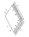
図1に示すように、アクティブマトリクス型液晶表示装置10は、光透過型の液晶表示装置として構成され、例えば、対角12.1インチの表示領域30を備えている。
【0012】
この液晶表示装置10は、液晶表示パネル12、液晶表示パネルを駆動するための信号線駆動回路基板14、走査線駆動回路基板16、各駆動回路基板と液晶表示パネルとを電気的に接続した複数のテープキャリアパッケージ(TCPと称する)18を備えている。
【0013】
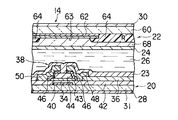
図1ないし図3に示すように、液晶表示パネル12はアレイ基板20および対向基板22を備え、これら基板は、周縁部を図示しないシール剤によって貼り合わせることにより、所定のギャップをおいて対向配置されている。そして、アレイ基板20と対向基板22との間には、それぞれ配向膜23、24を介して、光変調層としての液晶組成物26が封入されている。アレイ基板20および対向基板22の外表面には、それぞれ偏光板28、30が、その偏光軸が直交するように配置されている。
【0014】
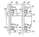
アレイ基板20は絶縁基板としてのガラス基板31を有し、このガラス基板上には、配線として多数の信号線32と多数の走査線34とがほぼ直交するようにマトリクス状に設けられている。信号線32と走査線34とで囲まれる領域には、それぞれITOからなる画素電極36が設けられ、各画素電極は、スイッチング素子としての薄膜トランジスタ(以下TFTと称する)38を介して、信号線32と走査線34との交差部に接続されている。
【0015】
各画素電極36はほぼ矩形状に形成され、1画素を構成している。1画素の寸法は、80μm×240μmである。信号線32はアレイ基板20の長辺側に引き出され、TCP18を介して信号線駆動回路基板14に接続されている。また、走査線34はアレイ基板20の短辺側に引き出され、TCP18を介して走査線駆動回路16に接続されている。
【0016】
図2および図3に示すように、各TFT38は、走査線34自体をゲート電極40とし、ゲート電極上に酸化シリコン、窒化シリコン等の誘電体層からなるゲート絶縁膜42が配置され、更に、ゲート絶縁膜42上にはa−Si膜からなる半導体膜43が形成されている。また、半導体膜43上には、走査線34に自己整合されて成るチャネル保護膜44として窒化シリコン膜が配置されている。
【0017】
そして、半導体膜43は、低抵抗半導体膜46として配置されたn+型a−Si膜およびソース電極48を介して画素電極36に電気的に接続されている。また、半導体膜43は、低抵抗半導体膜46として配置されるn+型a−Si膜および信号線32から延出したドレイン電極50を介して信号線32に電気的に接続されている。
【0018】
一方、対向基板22は透明なガラス基板60を備え、このガラス基板上には、クロム(Cr)の酸化膜からなる第1遮光層62、および第1遮光層上に積層されたクロム(Cr)から成る第2遮光層63が形成されている。これら第1および第2遮光層62、63は、アレイ基板20上のTFT38、信号線32と画素電極36との間隙、および走査線34と画素電極36との間隙をそれぞれを遮光するように、マトリクス状に形成されている。また、ガラス基板60上において、アレイ基板20側の画素電極36と対向する位置には、赤(R)、緑(G)、青(B)のカラーフィルタ層64が形成されている。
【0019】
上記構成の液晶表示パネル12において、アレイ基板20を製造する場合には、ガラス基板31上に複数の導電体層、誘電体層を形成し、各層を所定パターンにフォトエッチングすることにより、上述した信号線、走査線、画素電極、ゲート絶縁膜、TFT等を形成している。
【0020】
例えば、画素電極を形成する場合には、ガラス基板31全面にITO層を形成し、その上にレジスト層を形成した後、このレジスト層を所定パターンに露光し、更に、エッチングすることにより形成する。
【0021】
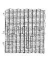
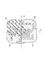
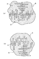
本実施の形態によれば、レジスト層を露光する際、ガラス基板31を複数の領域、例えば、図4に示すように、6つの領域A〜Fに分割して露光を行う。各領域はほぼ矩形状をなし、隣合う分割領域間の境界領域70の中心線は、水平に延びる水平境界線aおよびこれと直交する2本の垂直境界線bとで構成されている。
【0022】
図5に示すように、各分割領域の水平および垂直方向の境界線は、ほぼパルス波形状にジグザグに形成され、隣合う分割領域の境界線と噛み合って境界領域70を構成している。このように各分割領域の境界線をジグザグに形成し、境界領域70内で勾配を持たせることにより、境界領域70の光学的な特性変化の勾配を緩衝化し、水平および垂直方向の境界線はほとんど視認できず目立たなくすることができる。
【0023】
また、図6に示すように、水平境界線aと垂直境界線bとが直交する十字部分において、隣合う4つの分割領域A、B、D、E(あるいはB、C、E、F)の内、少なくとも1つの分割領域の境界線は、交点に対して対角方向に隣接する他の分割領域内まで延出したパターンを持って形成されている。
【0024】
図6に示す実施の形態によれば、分割領域Aの境界線は、水平方向に隣接する分割領域B、垂直方向に隣接する分割領域D、および対角方向に隣接する分割領域Eにも延出したパターンを有している。分割領域Dの境界線は、水平方向に隣接する分割領域E、垂直方向に隣接する分割領域A、および対角方向に隣接する分割領域Bにも延出している。更に、分割領域Eの境界線は、水平方向に隣接する分割領域D、垂直方向に隣接する分割領域B、および対角方向に隣接する分割領域Aにも延出したパターンを有している。
【0025】
分割領域の境界線を上記のように形成することにより、水平境界線aと垂直境界線bとが直交する十字部分においても、分割領域間の継ぎ目を目立たせなくすることができる。
【0026】
これまでの実験結果から、従来、分割領域間の透過率の差が0.5%以上あれば継ぎ目が認識されたが、本実施の形態に係る液晶表示パネルでは、隣合う分割領域間に1%の透過率の差があった場合でも、全く継ぎ目が認識されることはなかった。
【0027】
以上のように構成された液晶表示装置の製造方法によれば、アレイ基板20の導電体層および誘電体層をそれぞれパターニングする際、複数の領域に分割して露光するとともに、各分割領域の境界線をジグザグに形成し、かつ、水平および垂直境界線が十字状に直交する部分において、少なくとも1つの分割領域の境界線を対角方向に隣接した他の分割領域内まで延出させる構成としたことから、分割領域の継ぎ目を目立たなくし、良好な表示品位を有する液晶表示装置を製造することができる。
【0028】
なお、この発明は上述した実施の形態に限定されることなく、この発明の範囲内で種々変形可能である。例えば、上記実施の形態においては、ガラス基板を6つの領域に分割して露光する構成としたが、分割数は必要に応じて増減可能である。
【0029】
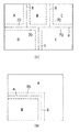
また、分割領域は、互いに同一の形状および寸法を有している場合に限らず、異なる寸法の分割領域としてもよい。例えば、図7(a)に示すように、水平分割線aと垂直分割線bとがT字状に交わるように、ガラス基板を5つに分割露光し、あるいは、図7(b)に示すように、水平分割線aと垂直分割線bとがL字状に交わるように、ガラス基板を2つに分割露光してもよい。
【0030】
図7(a)に示す分割露光の場合、各分割領域の水平および垂直境界線をジグザグに形成し境界領域内で噛み合わせるとともに、T字状の交差部においては、図8(a)に示すように、水平方向に隣合う少なくとも1つの分割領域の境界線は、交差部に対して対角方向にも延出したパターンを有して形成されている。
【0031】
図7(b)に示す分割露光の場合、各分割領域の水平および垂直境界線をジグザグに形成し境界領域内で噛み合わせるとともに、L字状の交差部において、図8(b)に示すように、少なくとも一方の分割領域の境界線は、交差部に対して対角方向にも延出したパターンを有して形成されている。
【0032】
上記図7(a)、7(b)、8(a)、8(b)に示す場合においも、前述した実施の形態と同様に、分割領域間の継ぎ目を目立たなくし、良好な表示品位を有する液晶表示装置を製造することが可能となる。
【0033】
【発明の効果】
以上詳述したように、この発明によれば、分割露光を行なう際、境界中心線が交差する十字部分、T字部分、L字部分においても分割領域間の継ぎ目を目立たせなくすることができ、表示品位の優れた大面積の液晶表示装置を製造可能な製造方法を提供することができる。
【図面の簡単な説明】
【図1】この発明に係る製造方法によって製造されるアクティブマトリクス型液晶表示装置の一例を示す斜視図。
【図2】上記アクティブマトリクス型液晶表示装置のアレイ基板を概略的に示す平面図。
【図3】図2の線A−Aに沿った断面図。
【図4】上記アレイ基板を、この発明の実施の形態に係る製造方法によって分割露光する際の分割領域を示す平面図。
【図5】図4における垂直境界領域の一部Gを拡大して示す平面図。
【図6】図4における十字状交差部Hを拡大して模式的に示す平面図。
【図7】この発明の変形例に係る製造方法の分割露光領域をそれぞれ示す平面図。
【図8】T字状交差部およびL字状交差部をそれぞれ拡大して模式的に示す平面図。
【符号の説明】
14…液晶表示パネル
20…アレイ基板
22…対向基板
26…液晶組成物
31…ガラス基板
32…信号線
34…走査線
36…画素電極
38…TFT
70…境界領域
a…水平境界線
b…垂直境界線
A、B、C、D、E、F…分割領域[0001]
BACKGROUND OF THE INVENTION
The present invention relates to a method for manufacturing an active matrix liquid crystal display device.
[0002]
[Prior art]
Liquid crystal display devices are widely used as display devices for notebook personal computers, warbros, small TVs and the like because of their thinness, light weight, and low power consumption. Among them, an active matrix type liquid crystal display device is expected as a large-sized TV and the like because it is capable of high-speed response, high contrast, and multi-gradation display.
[0003]
The liquid crystal display device is composed of electrodes such as signal lines and scanning lines, and elements such as thin film transistors, and is manufactured by a thin film formation process, a PEP process for forming a photoresist mask, and an etching process for removing unnecessary portions of the thin film. This is done by repeating the above.
[0004]
In recent years, a manufacturing apparatus corresponding to a large screen has been demanded as the screen has been increased. However, with regard to the exposure of the photoresist, it is possible to cope with a large screen by using a conventional small exposure apparatus by performing divided exposure in which the screen is divided into a plurality of areas.
[0005]
In general, when divided exposure is performed, deviations at the time of exposure may be visually recognized on divided lines. As a countermeasure, divided lines are formed with folded or island-shaped regions, and the boundary characteristic change gradient is buffered to joints. Is not conspicuous.
[0006]
[Problems to be solved by the invention]
It is common to form intersections and intersecting parts of horizontal and vertical dividing lines with straight lines, but if the area of horizontal and vertical dividing lines is made large so that the boundary is not conspicuous, the straight line also becomes large. There is a problem that the shift is visually recognized in the straight line portion. That is, when the width of the portion where adjacent regions are engaged with each other is made larger, the joint is not conspicuous, but a straight portion that is not divided into islands is recognized.
[0007]
The present invention has been made in view of the above points, and an object thereof is to provide a method of manufacturing a liquid crystal display device capable of manufacturing a large-area liquid crystal display device having a good display quality without conspicuous seams. is there.
[0008]
[Means for Solving the Problems]
In order to achieve the above object, according to the manufacturing method of the present invention, at least one of a conductor layer and a dielectric layer formed on an insulating substrate is divided into a plurality of regions, exposed, and patterned for each divided region. In the manufacturing method of the liquid crystal display device for forming pixels of a predetermined arrangement by forming the boundary line of each divided region in a zigzag manner and meshing with the boundary line of another adjacent divided region,
At the intersection where the horizontal boundary line that divides the divided area in the horizontal direction and the vertical boundary line that divides in the vertical direction intersect, the zigzag boundary lines of two diagonally adjacent divided areas are each divided into one part It is characterized by having a pattern extending from one region to the other divided region and meshing with each other.
[0009]
According to the above-described configuration, the gradient of the optical characteristic change in the boundary region can be buffered even at a portion where the horizontally dividing boundary line and the vertically dividing boundary line intersect or intersect when dividing exposure is performed. . Thereby, it is possible to manufacture a liquid crystal display device having a good display quality, in which the joints between the divided regions are not conspicuous.
[0010]
DETAILED DESCRIPTION OF THE INVENTION
Hereinafter, a manufacturing method of an active matrix liquid crystal display device according to an embodiment of the present invention will be described in detail with reference to the drawings. First, an example of an active matrix liquid crystal display device will be described.
[0011]
As shown in FIG. 1, the active matrix liquid
[0012]
The liquid
[0013]
As shown in FIGS. 1 to 3, the liquid
[0014]
The
[0015]
Each
[0016]
As shown in FIGS. 2 and 3, each
[0017]
The
[0018]
On the other hand, the
[0019]
When the
[0020]
For example, when forming a pixel electrode, an ITO layer is formed on the entire surface of the
[0021]
According to the present embodiment, when exposing the resist layer, the
[0022]
As shown in FIG. 5, the horizontal and vertical boundary lines of each divided area are formed in a substantially zigzag shape in a pulse wave shape, and mesh with the boundary lines of adjacent divided areas to form a
[0023]
Further, as shown in FIG. 6, in the cross portion where the horizontal boundary line a and the vertical boundary line b are orthogonal to each other, four adjacent divided areas A, B, D, E (or B, C, E, F) Among them, the boundary line of at least one divided region is formed with a pattern extending to another divided region adjacent to the intersection in the diagonal direction.
[0024]
According to the embodiment shown in FIG. 6, the boundary line of the divided area A extends to the divided area B adjacent in the horizontal direction, the divided area D adjacent in the vertical direction, and the divided area E adjacent in the diagonal direction. It has a released pattern. The boundary lines of the divided areas D also extend to the divided areas E adjacent in the horizontal direction, the divided areas A adjacent in the vertical direction, and the divided areas B adjacent in the diagonal direction. Further, the boundary line of the divided region E has a pattern extending to the divided region D adjacent in the horizontal direction, the divided region B adjacent in the vertical direction, and the divided region A adjacent in the diagonal direction.
[0025]
By forming the boundary lines of the divided areas as described above, the joint between the divided areas can be made inconspicuous even in the cross portion where the horizontal boundary line a and the vertical boundary line b are orthogonal to each other.
[0026]
From the experimental results so far, the seam has been conventionally recognized if the difference in transmittance between the divided regions is 0.5% or more. However, in the liquid crystal display panel according to the present embodiment, 1 between adjacent divided regions is recognized. Even when there was a difference in transmittance of%, no seam was recognized.
[0027]
According to the manufacturing method of the liquid crystal display device configured as described above, when patterning the conductor layer and the dielectric layer of the
[0028]
The present invention is not limited to the above-described embodiment, and various modifications can be made within the scope of the present invention. For example, in the above embodiment, the glass substrate is divided into six regions for exposure, but the number of divisions can be increased or decreased as necessary.
[0029]
Further, the divided areas are not limited to having the same shape and dimensions, and may be divided areas having different dimensions. For example, as shown in FIG. 7 (a), the glass substrate is divided into five pieces so that the horizontal dividing line a and the vertical dividing line b intersect in a T shape, or as shown in FIG. 7 (b). As described above, the glass substrate may be divided and exposed in two so that the horizontal dividing line a and the vertical dividing line b intersect in an L shape.
[0030]
In the case of the divided exposure shown in FIG. 7A, the horizontal and vertical boundary lines of each divided region are formed in a zigzag and meshed within the boundary region, and the T-shaped intersection is shown in FIG. 8A. As described above, the boundary line of at least one divided region adjacent in the horizontal direction has a pattern extending diagonally with respect to the intersection.
[0031]
In the case of the divided exposure shown in FIG. 7B, the horizontal and vertical boundary lines of each divided region are formed in a zigzag and meshed within the boundary region, and at the L-shaped intersection, as shown in FIG. 8B. In addition, the boundary line of at least one of the divided regions is formed having a pattern extending diagonally with respect to the intersecting portion.
[0032]
In the case shown in FIGS. 7A, 7B, 8A, and 8B, as in the above-described embodiment, the seam between the divided areas is made inconspicuous, and a good display quality is obtained. A liquid crystal display device having the same can be manufactured.
[0033]
【The invention's effect】
As described above in detail, according to the present invention, when performing the divided exposure, the joint between the divided regions can be made inconspicuous even in the cross portion, the T-shaped portion, and the L-shaped portion where the boundary center line intersects. It is possible to provide a manufacturing method capable of manufacturing a large-area liquid crystal display device with excellent display quality.
[Brief description of the drawings]
FIG. 1 is a perspective view showing an example of an active matrix liquid crystal display device manufactured by a manufacturing method according to the present invention.
FIG. 2 is a plan view schematically showing an array substrate of the active matrix liquid crystal display device.
3 is a cross-sectional view taken along line AA in FIG.
FIG. 4 is a plan view showing a divided area when the array substrate is subjected to divided exposure by the manufacturing method according to the embodiment of the present invention;
5 is an enlarged plan view showing a part G of a vertical boundary region in FIG. 4. FIG.
6 is a plan view schematically showing an enlarged cross-shaped intersection H in FIG. 4;
FIG. 7 is a plan view showing divided exposure regions of a manufacturing method according to a modification of the present invention.
FIG. 8 is a plan view schematically showing an enlarged T-shaped intersection and an L-shaped intersection, respectively.
[Explanation of symbols]
14 ... Liquid
70 ... boundary area a ... horizontal boundary line b ... vertical boundary lines A, B, C, D, E, F ... divided areas
Claims (4)
上記分割領域を水平方向に分割する水平境界線と垂直方向に分割する垂直境界線とが交差する交差部において、対角方向に隣接する2つの分割領域のジグザグの境界線は、それぞれ一方の分割領域から他方の分割領域内まで延出し相互に噛み合ったパターンを有していることを特徴とする液晶表示装置の製造方法。When at least one of the conductor layer and the dielectric layer formed on the insulating substrate is divided into a plurality of regions and exposed and patterned for each divided region, a boundary line of each divided region is formed in a zigzag, In a manufacturing method of a liquid crystal display device that forms pixels of a predetermined arrangement by meshing with a boundary line of another adjacent divided region,
At the intersection where the horizontal boundary line that divides the divided area in the horizontal direction and the vertical boundary line that divides in the vertical direction intersect, the zigzag boundary lines of two diagonally adjacent divided areas are each divided into one part A method of manufacturing a liquid crystal display device, comprising a pattern extending from one region to the other divided region and meshing with each other .
Priority Applications (4)
| Application Number | Priority Date | Filing Date | Title |
|---|---|---|---|
| JP06109098A JP3998317B2 (en) | 1998-03-12 | 1998-03-12 | Manufacturing method of liquid crystal display device |
| TW088103675A TW500963B (en) | 1998-03-12 | 1999-03-10 | Method of manufacturing liquid-crystal display device having a plurality of divided regions |
| KR1019990008024A KR100329210B1 (en) | 1998-03-12 | 1999-03-11 | Method for manufacturing liquid crystal display device |
| US09/266,801 US6157433A (en) | 1998-03-12 | 1999-03-12 | Method of manufacturing liquid-crystal display device having a plurality of divided regions |
Applications Claiming Priority (1)
| Application Number | Priority Date | Filing Date | Title |
|---|---|---|---|
| JP06109098A JP3998317B2 (en) | 1998-03-12 | 1998-03-12 | Manufacturing method of liquid crystal display device |
Publications (2)
| Publication Number | Publication Date |
|---|---|
| JPH11258629A JPH11258629A (en) | 1999-09-24 |
| JP3998317B2 true JP3998317B2 (en) | 2007-10-24 |
Family
ID=13161047
Family Applications (1)
| Application Number | Title | Priority Date | Filing Date |
|---|---|---|---|
| JP06109098A Expired - Fee Related JP3998317B2 (en) | 1998-03-12 | 1998-03-12 | Manufacturing method of liquid crystal display device |
Country Status (4)
| Country | Link |
|---|---|
| US (1) | US6157433A (en) |
| JP (1) | JP3998317B2 (en) |
| KR (1) | KR100329210B1 (en) |
| TW (1) | TW500963B (en) |
Families Citing this family (12)
| Publication number | Priority date | Publication date | Assignee | Title |
|---|---|---|---|---|
| JP4559590B2 (en) * | 2000-06-15 | 2010-10-06 | 東芝モバイルディスプレイ株式会社 | Substrate manufacturing method |
| JP4401551B2 (en) | 2000-09-21 | 2010-01-20 | エーユー オプトロニクス コーポレイション | Method for manufacturing liquid crystal display device, method for manufacturing display device, and liquid crystal display device |
| JP4619508B2 (en) * | 2000-09-27 | 2011-01-26 | シャープ株式会社 | Pattern forming method, thin film transistor matrix substrate manufacturing method, and exposure mask |
| US6903719B2 (en) * | 2001-01-26 | 2005-06-07 | Xerox Corporation | Rotation and threshold mechanism for twisting ball display |
| JP2002357835A (en) * | 2001-03-28 | 2002-12-13 | Toshiba Corp | LCD module |
| JP5019190B2 (en) * | 2001-06-26 | 2012-09-05 | 株式会社ジャパンディスプレイセントラル | Manufacturing method of liquid crystal display device and mask manufacturing apparatus |
| JP2004219991A (en) * | 2002-12-27 | 2004-08-05 | Sharp Corp | Display device substrate and liquid crystal display device having the same |
| KR100968566B1 (en) * | 2003-07-24 | 2010-07-08 | 삼성전자주식회사 | Liquid crystal display device and method for manufacturing display panel included therein |
| TWI225961B (en) * | 2003-11-17 | 2005-01-01 | Au Optronics Corp | Method of fabricating a liquid crystal display |
| JP4695382B2 (en) * | 2004-11-17 | 2011-06-08 | 東芝モバイルディスプレイ株式会社 | Method for designing exposure mask of flat display device |
| US7898641B2 (en) * | 2004-12-02 | 2011-03-01 | Sharp Kabushiki Kaisha | Production process of a display device, and a display device |
| KR102661702B1 (en) * | 2018-12-28 | 2024-05-02 | 삼성디스플레이 주식회사 | Foldable display device and manufacturing method thereof |
Family Cites Families (11)
| Publication number | Priority date | Publication date | Assignee | Title |
|---|---|---|---|---|
| US4878086A (en) * | 1985-04-01 | 1989-10-31 | Canon Kabushiki Kaisha | Flat panel display device and manufacturing of the same |
| FR2593632B1 (en) * | 1986-01-27 | 1988-03-18 | Maurice Francois | ACTIVE MATRIX DISPLAY SCREEN AND METHODS OF MAKING SAME |
| JPH01217325A (en) * | 1988-02-25 | 1989-08-30 | Sharp Corp | Liquid crystal display device |
| JP2600929B2 (en) * | 1989-01-27 | 1997-04-16 | 松下電器産業株式会社 | Liquid crystal image display device and method of manufacturing the same |
| US5162931A (en) * | 1990-11-06 | 1992-11-10 | Honeywell, Inc. | Method of manufacturing flat panel backplanes including redundant gate lines and displays made thereby |
| JPH0519301A (en) * | 1991-07-12 | 1993-01-29 | Toshiba Corp | Active matrix type liquid crystal display device |
| JP3067362B2 (en) * | 1991-12-19 | 2000-07-17 | ソニー株式会社 | Liquid crystal panel manufacturing method |
| JPH05341315A (en) * | 1992-06-08 | 1993-12-24 | Hitachi Ltd | Thin film transistor substrate, liquid crystal display panel and liquid crystal display device |
| WO1995016276A1 (en) * | 1993-12-07 | 1995-06-15 | Kabushiki Kaisha Toshiba | Display device and its manufacture |
| KR970006733B1 (en) * | 1993-12-14 | 1997-04-29 | 엘지전자 주식회사 | Method of manufacturing thin film transistor |
| US5916735A (en) * | 1996-11-21 | 1999-06-29 | Matsushita Electric Industrial Co., Ltd. | Method for manufacturing fine pattern |
-
1998
- 1998-03-12 JP JP06109098A patent/JP3998317B2/en not_active Expired - Fee Related
-
1999
- 1999-03-10 TW TW088103675A patent/TW500963B/en active
- 1999-03-11 KR KR1019990008024A patent/KR100329210B1/en not_active Expired - Fee Related
- 1999-03-12 US US09/266,801 patent/US6157433A/en not_active Expired - Lifetime
Also Published As
| Publication number | Publication date |
|---|---|
| JPH11258629A (en) | 1999-09-24 |
| KR100329210B1 (en) | 2002-03-21 |
| KR19990077763A (en) | 1999-10-25 |
| TW500963B (en) | 2002-09-01 |
| US6157433A (en) | 2000-12-05 |
Similar Documents
| Publication | Publication Date | Title |
|---|---|---|
| JP4733844B2 (en) | Thin film transistor substrate for liquid crystal display device and repair method thereof | |
| JP3289099B2 (en) | Active matrix type liquid crystal display device and manufacturing method thereof | |
| KR101254561B1 (en) | Array substrate for in-plane switching mode liquid crystal display device | |
| JP2005346054A (en) | Liquid crystal display device and manufacturing method thereof | |
| JP2005018079A (en) | Thin film transistor display panel and liquid crystal display device including the same | |
| JP3998317B2 (en) | Manufacturing method of liquid crystal display device | |
| JPH11153798A (en) | Active matrix type liquid crystal display | |
| KR100586245B1 (en) | Liquid Crystal Display Manufacturing Method | |
| JP3167633B2 (en) | Liquid crystal display | |
| KR100482167B1 (en) | LCD and its manufacturing method | |
| KR101167312B1 (en) | Method of forming fine pattern, liquid crystal display using the same, and fabricating method thereof | |
| JPH1195231A (en) | Liquid crystal display | |
| JP2005025206A (en) | Color filter display plate and liquid crystal display device including the same | |
| KR101333594B1 (en) | Liquid crystal display device and method of fabricating the same | |
| JP3105183B2 (en) | Active matrix type liquid crystal display | |
| JP3853946B2 (en) | Active matrix liquid crystal display device | |
| KR20020050021A (en) | array panel of liquid crystal display and manufacturing method thereof | |
| JP2851305B2 (en) | Liquid crystal display | |
| JP4406173B2 (en) | Liquid crystal display | |
| KR101622180B1 (en) | In plane switching mode liquid crystal display device and method of fabricating the same | |
| JPH04184323A (en) | Liquid crystal display device | |
| KR102056687B1 (en) | Liquid Crystal Display Device and Method for Fabricating the same | |
| KR100949498B1 (en) | Mask for liquid crystal display and exposure method of liquid crystal display using same | |
| JP2000122092A (en) | Transistor array substrate and liquid crystal display device | |
| JPS6270815A (en) | Liquid crystal device |
Legal Events
| Date | Code | Title | Description |
|---|---|---|---|
| A621 | Written request for application examination |
Free format text: JAPANESE INTERMEDIATE CODE: A621 Effective date: 20050302 |
|
| A977 | Report on retrieval |
Free format text: JAPANESE INTERMEDIATE CODE: A971007 Effective date: 20070216 |
|
| A131 | Notification of reasons for refusal |
Free format text: JAPANESE INTERMEDIATE CODE: A131 Effective date: 20070306 |
|
| A521 | Written amendment |
Free format text: JAPANESE INTERMEDIATE CODE: A523 Effective date: 20070501 |
|
| A711 | Notification of change in applicant |
Free format text: JAPANESE INTERMEDIATE CODE: A711 Effective date: 20070514 |
|
| TRDD | Decision of grant or rejection written | ||
| A01 | Written decision to grant a patent or to grant a registration (utility model) |
Free format text: JAPANESE INTERMEDIATE CODE: A01 Effective date: 20070731 |
|
| A61 | First payment of annual fees (during grant procedure) |
Free format text: JAPANESE INTERMEDIATE CODE: A61 Effective date: 20070807 |
|
| R150 | Certificate of patent or registration of utility model |
Free format text: JAPANESE INTERMEDIATE CODE: R150 |
|
| FPAY | Renewal fee payment (event date is renewal date of database) |
Free format text: PAYMENT UNTIL: 20100817 Year of fee payment: 3 |
|
| S533 | Written request for registration of change of name |
Free format text: JAPANESE INTERMEDIATE CODE: R313533 |
|
| FPAY | Renewal fee payment (event date is renewal date of database) |
Free format text: PAYMENT UNTIL: 20100817 Year of fee payment: 3 |
|
| R350 | Written notification of registration of transfer |
Free format text: JAPANESE INTERMEDIATE CODE: R350 |
|
| FPAY | Renewal fee payment (event date is renewal date of database) |
Free format text: PAYMENT UNTIL: 20100817 Year of fee payment: 3 |
|
| FPAY | Renewal fee payment (event date is renewal date of database) |
Free format text: PAYMENT UNTIL: 20110817 Year of fee payment: 4 |
|
| FPAY | Renewal fee payment (event date is renewal date of database) |
Free format text: PAYMENT UNTIL: 20120817 Year of fee payment: 5 |
|
| S531 | Written request for registration of change of domicile |
Free format text: JAPANESE INTERMEDIATE CODE: R313531 |
|
| FPAY | Renewal fee payment (event date is renewal date of database) |
Free format text: PAYMENT UNTIL: 20120817 Year of fee payment: 5 |
|
| R350 | Written notification of registration of transfer |
Free format text: JAPANESE INTERMEDIATE CODE: R350 |
|
| S533 | Written request for registration of change of name |
Free format text: JAPANESE INTERMEDIATE CODE: R313533 |
|
| FPAY | Renewal fee payment (event date is renewal date of database) |
Free format text: PAYMENT UNTIL: 20120817 Year of fee payment: 5 |
|
| R350 | Written notification of registration of transfer |
Free format text: JAPANESE INTERMEDIATE CODE: R350 |
|
| FPAY | Renewal fee payment (event date is renewal date of database) |
Free format text: PAYMENT UNTIL: 20120817 Year of fee payment: 5 |
|
| FPAY | Renewal fee payment (event date is renewal date of database) |
Free format text: PAYMENT UNTIL: 20130817 Year of fee payment: 6 |
|
| R250 | Receipt of annual fees |
Free format text: JAPANESE INTERMEDIATE CODE: R250 |
|
| R250 | Receipt of annual fees |
Free format text: JAPANESE INTERMEDIATE CODE: R250 |
|
| R250 | Receipt of annual fees |
Free format text: JAPANESE INTERMEDIATE CODE: R250 |
|
| R250 | Receipt of annual fees |
Free format text: JAPANESE INTERMEDIATE CODE: R250 |
|
| LAPS | Cancellation because of no payment of annual fees |