JP3997611B2 - Piezoelectric oscillator - Google Patents
Piezoelectric oscillator Download PDFInfo
- Publication number
- JP3997611B2 JP3997611B2 JP17257198A JP17257198A JP3997611B2 JP 3997611 B2 JP3997611 B2 JP 3997611B2 JP 17257198 A JP17257198 A JP 17257198A JP 17257198 A JP17257198 A JP 17257198A JP 3997611 B2 JP3997611 B2 JP 3997611B2
- Authority
- JP
- Japan
- Prior art keywords
- heater
- land pattern
- piezoelectric vibrator
- piezoelectric
- circuit board
- Prior art date
- Legal status (The legal status is an assumption and is not a legal conclusion. Google has not performed a legal analysis and makes no representation as to the accuracy of the status listed.)
- Expired - Fee Related
Links
Images


Description
【0001】
【発明の属する技術分野】
本発明は圧電発振器に関し、特に、発振周波数が高安定な圧電発振器に関する。
【0002】
【従来の技術】
移動通信基地局の通信設備のメンテナンス等の為に使用する周波数カウンタや衛星通信器等の電気機器分野に於いては、これらの基準信号発信源として一般に周波数安定度が1×10⁻⁷〜1×10⁻¹⁰程度の高安定な恒温槽型水晶発振器を使用する。
更に、近年これらの分野に於いても小型、軽量化が求められており、それに使用する恒温槽型水晶発振器に対しても小型、軽量化の要請が高い。
しかし、従来の一般的な恒温槽型水晶発振器は高安定な発振周波数を得る為に水晶振動子を熱容量が大きな金属製のブロックの凹所内に収納し、更に、金属ブロックを所定の温度にて加熱する構成としており、この金属ブロックが大型である為に発振器の大型化が避けられないという問題があった 。
【0003】
そこで、小型化を達成する為に金属ブロックを用いない高安定型水晶発振器が提案されており、図3はその高安定水晶発振器の構造図を示したものである。
同図(a)は側面構造図であり、同図(b)は上面構造図を示したものである。同図に示すプリント基板101の下面には発振回路102と温度制御回路103とを配置し、前記プリント基板101の上面には6個の表面実装型小型ヒータ104、104'、105、105'、106、106'を互いにほぼ等間隔に配置している。
また、前記小型ヒータ106と106'との間の前記プリント基板101上に温度センサ111を配置し、該温度センサ111は前記温度制御回路103と電気的に接続している。
前記小型ヒータ104、104'、105、105'は何れも水晶振動子107の金属キャップ108と前記プリント基板101との間に密着固定されている。
一方、前記小型ヒータ106、106'は前記水晶振動子107のリード端子109、109'と前記プリント基板101との間に金属片110、110'を介して密着固定されている。
前記小型ヒータ104、104'、105、105'、106、106'は何れも前記温度制御回路103により、水晶振動子107が一定の温度となるように制御されている。
更に、温度制御回路を構成するパワートランジスタ112はプリント基板の表側に配置され、そのコレクタを金属キャップ108と密着固定することによって補助熱源としても利用している。
【0004】
この様な構成の水晶発振器の動作についてその動作を説明する。
水晶発振器に電源を投入すると発振回路102は水晶振動子107の共振周波数に基づく周波数にて発振を開始する。
一方、温度制御回路103は温度センサ111が検知した温度と設定温度とを一致させるべく6個の前記小型ヒータに電力を供給する。
該小型ヒータ104、104'、105、105'は金属キャップ108を加熱し、該金属キャップ108からの放射熱によりキャップ内の水晶素板が暖められる。
前記小型ヒータ106、106'は前記リード端子109、109'を加熱し、該リード端子から直接伝搬する熱により水晶素板を暖める。
この様な構成とすることにより、個々の小型ヒータはその熱容量が小さいものであっても、複数これを用い、更に、直接に水晶振動子を加熱している為、十分に水晶振動子を設定温度に加熱及び、制御することを可能とし、小型で高安定な周波数を出力する水晶発振器を得ていた。
【0005】
【本発明が解決しようとする課題】
しかしながら、上記に説明した水晶発振器は複数の小型ヒータを用いている為、消費電流が大きくなり、これを用いた携帯機器はバッテリーによる駆動時間が短時間となるという問題が生じていた。
【0006】
【課題を解決するための手段】
上記課題を解決する為に本発明に係わる請求項1記載の発明は、圧電振動子と、発振回路と、加熱ヒータと、該加熱ヒータの加熱温度を制御する為の温度制御回路とをプリント基板上に配置した圧電発振器に於いて、前記温度制御回路は感温素子と直流制御用トランジスタとを備えたものであって、前記プリント基板の第1の主面に前記トランジスタのコレクタ端子を接続する為の広面積のランドパターンを設け、前記プリント基板上の第1の主面に少なくとも前記トランジスタとヒータと感温素子とを配置したものであって、前記圧電振動子を前記感温素子とヒータとを覆うように配置すると共に、前記圧電振動子と前記ランドパターンとの間を熱伝導部材を介して接続したことを特徴としている。
【0007】
請求項2記載の発明は請求項1記載の発明に加え、前記圧電振動子とランドパターンとの間を金属板を介して接続したことを特徴としている。
【0008】
請求項3記載の発明は請求項1または、請求項2記載の発明に加え、前記圧電振動子とランドパターンとの間に樹脂を充填したことを特徴としている。
【0009】
【本発明の実施の形態】
以下、図示した実施例に基づいて本発明を詳細に説明する。
図1(a)及び、(b)は本発明に基づく水晶発振器の一実施例を示す分解構成図と側面からの断面構造図とを示すものである。
この実施例では同図に示すようにプリント基板1の上面には表面実装型の小型ヒータ2が搭載されており、該小型ヒータ2の一方の端子は前記プリント基板上に設けられた広面積なランドパタン3と接続されている。
更に、前記ランドパターン3には前記小型ヒータ2と電気的に接続するパワートランジスタ4のコレクタ端子を接続する。
同図(a)に示すように前記小型ヒータ2の両脇にはそれぞれ等間隔に感熱素子としてサーミスタ5とサーミスタ5'とを配置する。
同図(b)に示すように発振回路6や温度制御回路7等を構成するその他の電子部品は、例えばプリント基板の裏面に配置する。
また、水晶振動子8には金属製のサポート9をはめ込み、また、該サポート9の周縁の一部には下側に突出する端子10が設けられている。
前記端子10は、前記水晶振動子8を前記プリント基板1上に搭載した際に、前記ランドパターン3と対応する位置に設けたものであり、熱伝導性に優れたハンダ等により前記端子10とランドパターン3とを固着する。
またこの時、水晶振動子8はヒータ2の上面と密着するよう配置される。
そして最後に、熱伝導性に優れた樹脂接着剤11を前記振動子8とプリント基板1との間に充填する。
尚、前記トランジスタのコレクタはアースと絶縁するよう考慮する。
【0010】
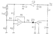
図2は図1に示すように各部品を配置した水晶発振器に使用する温度制御回路の一実施例を示した回路図である。
同図に於いて、サーミスタTH1とサーミスタTH2は図1の5、5'に、パワートランジスタTR1が図1の4に、該パワートランジスタTR1のコレクタに接続されているヒータH1が図1の2にそれぞれ相当する。
このような構成としたことにより水晶振動子6は小型ヒータ2からの熱が水晶振動子8の下側より直接伝達されると共に、前記小型ヒータ2と前記パワートランジスタ4のコレクタとによりランドパターン3が加熱され、更に、この熱が前記サポート9に設けた端子10及び、前記樹脂接着剤11とを介し晶振動子8に伝達されることになる。
パワートランジスタ4の熱を補助熱源として有効に利用すると共に、水晶振動子8に広面積なランドパターン3及び、樹脂接着剤11を用いて熱伝達される構造とした為、熱容量の小さい一つの小型ヒータによる加熱であっても十分に水晶振動子6を加熱することを可能にしている。
また、サーミスタ5、5'を水晶振動子8の両脇のそれぞれに配置し、温度検知点数を増やすことにより高感度な温度制御を可能にしている。
【0011】
【発明の効果】
以上説明したように前記請求項1記載の発明は、補助熱源であるパワートランジスタの熱を広面積なランドパターンに伝達し、更に、前記ランドパターンに伝達された熱を圧電振動子に伝達するよう構成することにより、効果的にパワートランジスタの熱が圧電振動子に伝達される為、前記圧電振動子を加熱する主要加熱素子として熱容量の少ない小型ヒータを用いることが可能となり、これにより圧電発振器の低消費電流化が可能となるという効果を奏する。
【0012】
請求項2記載の発明は請求項1記載の発明の効果に加え、前記ランドパターンに伝達されたパワートランジスタの熱が前記ランドパタンと圧電振動子との間に介在する金属板を介し効果的に前記圧電振動子に伝達されるよう構成した構成した為、圧電振動子を主要に加熱するヒータを熱容量の小さいものとすることが可能となり、これにより圧電発振器の低消費電流化が可能になるという効果を奏する。
【0013】
請求項3記載の発明は請求項1または、請求項2記載の発明に加え、前記ランドパターンに伝達されたパワートランジスタの熱が前記ランドパターンと圧電振動子との間に充填された樹脂を介し効果的に前記圧電振動子に伝達されるよう構成した為、圧電振動子を主要に加熱するヒータを熱容量の小さいものとすることが可能となり、これにより圧電発振器の低消費電流化が可能になるという効果を奏する。
【図面の簡単な説明】
【図1】本発明に基づく水晶発振器の一実施例の構成図を示すものである。
(a)本発明に基づく水晶発振器の一実施例の分解構成図を示すものである。
(b)本発明に基づく水晶発振器の一実施例の側面断面構造図を示すものである。
【図2】本発明に用いる温度制御回路の一実施例の回路図を示すものである。
【図3】従来の水晶発振器の構造図を示すものである。
(a)従来の水晶発振器の側面構造図を示すものである。
(b)従来の水晶発振器の上面構造図を示すものである。
【符号の説明】
1、101プリント基板、2小型ヒータ、3ランドパタン、4、112パワートランジスタ、5、5'サーミスタ、6、102発振回路、7、103温度制御回路、8、107水晶振動子、9サポート、10端子、11樹脂、104、104'、105、105'、106、106'小型ヒータ、108金属キャップ、109、109'端子、110、110'金属板、111温度センサ、[0001]
BACKGROUND OF THE INVENTION
The present invention relates to a piezoelectric oscillator, and more particularly to a piezoelectric oscillator having a highly stable oscillation frequency.
[0002]
[Prior art]
In the field of electrical equipment such as frequency counters and satellite communication devices used for maintenance of communication facilities of mobile communication base stations, the frequency stability is generally 1 × 10 −7 to 1 as a reference signal source. Use a highly stable thermostat crystal oscillator of about × 10 -10 .
Furthermore, in recent years, there is a demand for miniaturization and weight reduction in these fields, and there is a high demand for miniaturization and weight reduction for the thermostatic chamber crystal oscillator used therefor.
However, in order to obtain a high stable oscillation frequency, a conventional general thermostat crystal oscillator stores a crystal resonator in a recess of a metal block having a large heat capacity, and further, the metal block is placed at a predetermined temperature. There is a problem in that the size of the oscillator is unavoidable due to the large size of the metal block.
[0003]
Therefore, a highly stable crystal oscillator that does not use a metal block has been proposed in order to achieve miniaturization, and FIG. 3 shows a structural diagram of the highly stable crystal oscillator.
FIG. 4A is a side structural view, and FIG. 4B is a top structural view. An
Further, a temperature sensor 111 is disposed on the printed
Each of the
On the other hand, the
The
Further, the
[0004]
The operation of the crystal oscillator having such a configuration will be described.
When power is supplied to the crystal oscillator, the
On the other hand, the temperature control circuit 103 supplies power to the six small heaters so that the temperature detected by the temperature sensor 111 matches the set temperature.
The
The
By adopting such a configuration, even if each small heater has a small heat capacity, a plurality of these heaters are used, and the crystal resonator is directly heated. A crystal oscillator that can be heated and controlled to a temperature and outputs a small and highly stable frequency has been obtained.
[0005]
[Problems to be solved by the present invention]
However, since the crystal oscillator described above uses a plurality of small heaters, the current consumption increases, and there has been a problem that a portable device using this has a short drive time by a battery.
[0006]
[Means for Solving the Problems]
In order to solve the above-mentioned problems, a first aspect of the present invention relates to a printed circuit board comprising a piezoelectric vibrator, an oscillation circuit, a heater, and a temperature control circuit for controlling the heating temperature of the heater. In the piezoelectric oscillator disposed above, the temperature control circuit includes a temperature sensing element and a DC control transistor, and a collector terminal of the transistor is connected to a first main surface of the printed circuit board. A land pattern having a large area is provided, and at least the transistor, the heater, and the temperature sensitive element are arranged on the first main surface on the printed circuit board, and the piezoelectric vibrator is connected to the temperature sensitive element and the heater. And the piezoelectric vibrator and the land pattern are connected via a heat conductive member.
[0007]
The invention according to claim 2 is characterized in that, in addition to the invention according to claim 1, the piezoelectric vibrator and the land pattern are connected via a metal plate.
[0008]
The invention described in claim 3 is characterized in that, in addition to the invention described in claim 1 or 2, a resin is filled between the piezoelectric vibrator and the land pattern.
[0009]
[Embodiments of the Invention]
Hereinafter, the present invention will be described in detail based on illustrated embodiments.
FIGS. 1A and 1B are an exploded configuration diagram showing an embodiment of a crystal oscillator according to the present invention and a sectional structure diagram from the side.
In this embodiment, as shown in the same figure, a surface mount type small heater 2 is mounted on the upper surface of the printed circuit board 1, and one terminal of the small heater 2 has a large area provided on the printed circuit board. It is connected to the land pattern 3.
Further, a collector terminal of a power transistor 4 that is electrically connected to the small heater 2 is connected to the land pattern 3.
As shown in FIG. 2A, a
As shown in FIG. 5B, other electronic components that constitute the oscillation circuit 6, the temperature control circuit 7, and the like are disposed on the back surface of the printed circuit board, for example.
Further, a metal support 9 is fitted into the crystal resonator 8, and a terminal 10 protruding downward is provided at a part of the periphery of the support 9.
The terminal 10 is provided at a position corresponding to the land pattern 3 when the crystal resonator 8 is mounted on the printed circuit board 1. The terminal 10 is connected to the terminal 10 by solder having excellent thermal conductivity. The land pattern 3 is fixed.
At this time, the crystal unit 8 is disposed so as to be in close contact with the upper surface of the heater 2.
Finally, a resin adhesive 11 having excellent thermal conductivity is filled between the vibrator 8 and the printed board 1.
Note that the collector of the transistor is considered to be insulated from the ground.
[0010]
FIG. 2 is a circuit diagram showing an embodiment of a temperature control circuit used in the crystal oscillator in which the respective components are arranged as shown in FIG.
In the same figure, the thermistor TH1 and thermistor TH2 are shown in 5 and 5 'in FIG. 1, the power transistor TR1 is shown in 4 in FIG. 1, and the heater H1 connected to the collector of the power transistor TR1 is shown in 2 in FIG. Each corresponds.
With this configuration, the crystal resonator 6 directly transfers heat from the small heater 2 from the lower side of the crystal resonator 8, and the land pattern 3 is formed by the small heater 2 and the collector of the power transistor 4. Then, this heat is transmitted to the crystal oscillator 8 via the terminal 10 provided on the support 9 and the resin adhesive 11.
Since the heat of the power transistor 4 is effectively used as an auxiliary heat source and heat is transferred to the crystal resonator 8 by using the land pattern 3 having a large area and the resin adhesive 11, it is one small size having a small heat capacity. Even with heating by a heater, the crystal resonator 6 can be sufficiently heated.
Further, the
[0011]
【The invention's effect】
As described above, according to the first aspect of the present invention, the heat of the power transistor, which is an auxiliary heat source, is transmitted to the land pattern having a large area, and the heat transmitted to the land pattern is further transmitted to the piezoelectric vibrator. By configuring, the heat of the power transistor is effectively transferred to the piezoelectric vibrator, so that a small heater with a small heat capacity can be used as a main heating element for heating the piezoelectric vibrator. There is an effect that current consumption can be reduced.
[0012]
According to a second aspect of the present invention, in addition to the effect of the first aspect of the invention, the heat of the power transistor transmitted to the land pattern is effectively transmitted through a metal plate interposed between the land pattern and the piezoelectric vibrator. Since it is configured to be transmitted to the piezoelectric vibrator, the heater that mainly heats the piezoelectric vibrator can be made to have a small heat capacity, which makes it possible to reduce the current consumption of the piezoelectric oscillator. There is an effect.
[0013]
According to a third aspect of the invention, in addition to the first or second aspect of the invention, the heat of the power transistor transmitted to the land pattern is passed through a resin filled between the land pattern and the piezoelectric vibrator. Since it is configured so as to be effectively transmitted to the piezoelectric vibrator, it is possible to reduce the heat capacity of the heater that mainly heats the piezoelectric vibrator, and this makes it possible to reduce the current consumption of the piezoelectric oscillator. There is an effect.
[Brief description of the drawings]
FIG. 1 is a configuration diagram of an embodiment of a crystal oscillator according to the present invention.
(A) The exploded block diagram of one Example of the crystal oscillator based on this invention is shown.
(B) A side sectional structural view of an embodiment of a crystal oscillator according to the present invention is shown.
FIG. 2 is a circuit diagram of an embodiment of a temperature control circuit used in the present invention.
FIG. 3 is a structural diagram of a conventional crystal oscillator.
(A) The side surface structure figure of the conventional crystal oscillator is shown.
(B) A top structural view of a conventional crystal oscillator.
[Explanation of symbols]
1, 101 printed circuit board, 2 small heater, 3 land pattern, 4, 112 power transistor, 5, 5 'thermistor, 6, 102 oscillation circuit, 7, 103 temperature control circuit, 8, 107 crystal oscillator, 9 support, 10 Terminal, 11 resin, 104, 104 ′, 105, 105 ′, 106, 106 ′ small heater, 108 metal cap, 109, 109 ′ terminal, 110, 110 ′ metal plate, 111 temperature sensor,
Claims (3)
Priority Applications (6)
| Application Number | Priority Date | Filing Date | Title |
|---|---|---|---|
| JP17257198A JP3997611B2 (en) | 1998-06-19 | 1998-06-19 | Piezoelectric oscillator |
| DE69933615T DE69933615T2 (en) | 1998-01-20 | 1999-01-18 | PIEZO ELECTRIC OSCILLATOR |
| CA002283963A CA2283963C (en) | 1998-01-20 | 1999-01-18 | Piezo-oscillator |
| PCT/JP1999/000128 WO1999037018A1 (en) | 1998-01-20 | 1999-01-18 | Piezo-oscillator |
| EP99900335A EP0969591B1 (en) | 1998-01-20 | 1999-01-18 | Piezo-oscillator |
| US09/367,691 US6147565A (en) | 1998-01-20 | 1999-01-18 | Piezo-oscillator with heater and temperature control circuit |
Applications Claiming Priority (1)
| Application Number | Priority Date | Filing Date | Title |
|---|---|---|---|
| JP17257198A JP3997611B2 (en) | 1998-06-19 | 1998-06-19 | Piezoelectric oscillator |
Publications (3)
| Publication Number | Publication Date |
|---|---|
| JP2000013140A JP2000013140A (en) | 2000-01-14 |
| JP2000013140A5 JP2000013140A5 (en) | 2005-08-25 |
| JP3997611B2 true JP3997611B2 (en) | 2007-10-24 |
Family
ID=15944313
Family Applications (1)
| Application Number | Title | Priority Date | Filing Date |
|---|---|---|---|
| JP17257198A Expired - Fee Related JP3997611B2 (en) | 1998-01-20 | 1998-06-19 | Piezoelectric oscillator |
Country Status (1)
| Country | Link |
|---|---|
| JP (1) | JP3997611B2 (en) |
Families Citing this family (7)
| Publication number | Priority date | Publication date | Assignee | Title |
|---|---|---|---|---|
| JP2008136033A (en) * | 2006-11-29 | 2008-06-12 | Epson Toyocom Corp | Heat conducting tray for highly stable piezo-oscillator, tray unit, printed board unit and highly stable piezo-oscillator |
| JP5114122B2 (en) * | 2007-07-20 | 2013-01-09 | 日本電波工業株式会社 | Control circuit of thermostat in crystal oscillator with thermostat |
| JP4629760B2 (en) | 2008-09-02 | 2011-02-09 | 日本電波工業株式会社 | Constant temperature crystal oscillator |
| JP2011217224A (en) * | 2010-04-01 | 2011-10-27 | Seiko Epson Corp | Constant-temperature piezoelectric oscillator |
| JP5764922B2 (en) * | 2010-12-24 | 2015-08-19 | セイコーエプソン株式会社 | Temperature control circuit, thermostatic chamber type piezoelectric oscillator, electronic device, and temperature control method |
| JP6208472B2 (en) * | 2013-06-13 | 2017-10-04 | 日本電波工業株式会社 | Crystal oscillator with temperature chamber |
| JP6376330B2 (en) * | 2014-03-25 | 2018-08-22 | セイコーエプソン株式会社 | Electronic parts, electronic devices and mobile objects |
-
1998
- 1998-06-19 JP JP17257198A patent/JP3997611B2/en not_active Expired - Fee Related
Also Published As
| Publication number | Publication date |
|---|---|
| JP2000013140A (en) | 2000-01-14 |
Similar Documents
| Publication | Publication Date | Title |
|---|---|---|
| CA2283963C (en) | Piezo-oscillator | |
| EP1598931B1 (en) | Constant temperature type crystal oscillator | |
| JP2579915B2 (en) | Compact thermostat oscillator | |
| KR20100051862A (en) | Ovenized oscillator | |
| JP3997611B2 (en) | Piezoelectric oscillator | |
| US8212626B2 (en) | Constant-temperature type crystal oscillator | |
| JP4345549B2 (en) | Thin high stability piezoelectric oscillator and surface mount thin high stability piezoelectric oscillator | |
| JP2009284372A (en) | Constant temperature structure of crystal unit | |
| JPH07336141A (en) | Oscillator | |
| JP2000013140A5 (en) | ||
| JPH11214929A (en) | Piezoelectric oscillator | |
| JP4221814B2 (en) | Piezoelectric oscillator | |
| JP2000101346A (en) | Structure for highly stable piezoelectric oscillator | |
| JP4042471B2 (en) | Piezoelectric oscillator | |
| JP2005143060A (en) | Piezoelectric vibrator and piezoelectric oscillator using the same | |
| JP2001274626A (en) | Thin type highly stable piezoelectric oscillator | |
| JP2005045502A (en) | Heater unit for highly stable piezoelectric vibrator and highly stable piezoelectric vibrator | |
| JP2005203997A (en) | Crystal oscillator circuit | |
| JP2000077940A (en) | Piezo-oscillator | |
| JP2005117189A (en) | High stability piezoelectric oscillator | |
| JP2000101350A (en) | Piezoelectric oscillator | |
| KR200472685Y1 (en) | A portable carbon film thermostar | |
| JPH09260947A (en) | Crystal oscillator and temperature controlled crystal oscillator | |
| JPH10294618A (en) | Highly stable crystal oscillator having thermostatic structure | |
| JPH03153111A (en) | Acoustic surface wave oscillator |
Legal Events
| Date | Code | Title | Description |
|---|---|---|---|
| A521 | Written amendment |
Free format text: JAPANESE INTERMEDIATE CODE: A523 Effective date: 20050215 |
|
| A621 | Written request for application examination |
Free format text: JAPANESE INTERMEDIATE CODE: A621 Effective date: 20050215 |
|
| TRDD | Decision of grant or rejection written | ||
| A01 | Written decision to grant a patent or to grant a registration (utility model) |
Free format text: JAPANESE INTERMEDIATE CODE: A01 Effective date: 20070717 |
|
| A61 | First payment of annual fees (during grant procedure) |
Free format text: JAPANESE INTERMEDIATE CODE: A61 Effective date: 20070730 |
|
| R150 | Certificate of patent or registration of utility model |
Free format text: JAPANESE INTERMEDIATE CODE: R150 |
|
| FPAY | Renewal fee payment (event date is renewal date of database) |
Free format text: PAYMENT UNTIL: 20100817 Year of fee payment: 3 |
|
| FPAY | Renewal fee payment (event date is renewal date of database) |
Free format text: PAYMENT UNTIL: 20100817 Year of fee payment: 3 |
|
| FPAY | Renewal fee payment (event date is renewal date of database) |
Free format text: PAYMENT UNTIL: 20110817 Year of fee payment: 4 |
|
| FPAY | Renewal fee payment (event date is renewal date of database) |
Free format text: PAYMENT UNTIL: 20120817 Year of fee payment: 5 |
|
| FPAY | Renewal fee payment (event date is renewal date of database) |
Free format text: PAYMENT UNTIL: 20120817 Year of fee payment: 5 |
|
| S111 | Request for change of ownership or part of ownership |
Free format text: JAPANESE INTERMEDIATE CODE: R313111 |
|
| FPAY | Renewal fee payment (event date is renewal date of database) |
Free format text: PAYMENT UNTIL: 20120817 Year of fee payment: 5 |
|
| R371 | Transfer withdrawn |
Free format text: JAPANESE INTERMEDIATE CODE: R371 |
|
| FPAY | Renewal fee payment (event date is renewal date of database) |
Free format text: PAYMENT UNTIL: 20120817 Year of fee payment: 5 |
|
| S111 | Request for change of ownership or part of ownership |
Free format text: JAPANESE INTERMEDIATE CODE: R313111 |
|
| FPAY | Renewal fee payment (event date is renewal date of database) |
Free format text: PAYMENT UNTIL: 20120817 Year of fee payment: 5 |
|
| R350 | Written notification of registration of transfer |
Free format text: JAPANESE INTERMEDIATE CODE: R350 |
|
| FPAY | Renewal fee payment (event date is renewal date of database) |
Free format text: PAYMENT UNTIL: 20130817 Year of fee payment: 6 |
|
| S531 | Written request for registration of change of domicile |
Free format text: JAPANESE INTERMEDIATE CODE: R313531 |
|
| R350 | Written notification of registration of transfer |
Free format text: JAPANESE INTERMEDIATE CODE: R350 |
|
| LAPS | Cancellation because of no payment of annual fees |