JP3972011B2 - Fabrication method of ultrafine channel structure - Google Patents
Fabrication method of ultrafine channel structure Download PDFInfo
- Publication number
- JP3972011B2 JP3972011B2 JP2003066951A JP2003066951A JP3972011B2 JP 3972011 B2 JP3972011 B2 JP 3972011B2 JP 2003066951 A JP2003066951 A JP 2003066951A JP 2003066951 A JP2003066951 A JP 2003066951A JP 3972011 B2 JP3972011 B2 JP 3972011B2
- Authority
- JP
- Japan
- Prior art keywords
- thin film
- substrate
- oxide
- single crystal
- channel structure
- Prior art date
- Legal status (The legal status is an assumption and is not a legal conclusion. Google has not performed a legal analysis and makes no representation as to the accuracy of the status listed.)
- Expired - Fee Related
Links
Images


Description
【0001】
【産業上の利用分野】
本発明は、感度や効率が極めて高い半導体素子,発光素子,センサ,触媒,化学反応集積マイクロチップ媒体,DNAデバイス担持体,マイクロ燃料電池用素子としての使用が期待される超微細チャンネル構造を単結晶酸化物基体上に作り込む方法に関する。
【0002】
【従来の技術】
各種機能を呈する薄膜が積層されるサファイア単結晶等の絶縁基板は、機能薄膜に対する良好な接合状態を得るため所定の結晶面を表面に露出させた後で鏡面状態に研磨される。特定結晶面は、単結晶基板をダイヤモンドカッター等で切断する際に切断角度の調整によって基板表面に露出する。切断後の基板は、ダイヤモンド研磨粉を用いて研磨した後、コロイダルシリカ等を含む用液中で化学エッチングされる。機械研磨,化学研磨された単結晶基板は、表面粗さ1nm程度の極めて平滑な状態に鏡面仕上げされている。
【0003】
通常の半導体素子を搭載する場合、従来の機械研磨,化学研磨で鏡面仕上げされたサファイア単結晶基板でも十分に必要とする接続が得られる。しかし、高機能化,高密度化が急速に進行している機能素子を対象にするとき、機械研磨,化学研磨により鏡面仕上げされた平滑面では満足できる接続が得られない場合がある。たとえば、GaN青色発光素子を搭載したサファイア単結晶基板では、素子/基板間の接続が発光出力に大きく影響し、接続界面に乱れがあると青色発光の出力効率が低下する。SOS型(Silicon-On-Sapphire)では、シリコン薄膜/基板の界面に乱れがあると満足できる特性が得られない。
【0004】
【発明が解決しようとする課題】
高機能化,高密度化に伴う欠陥発生は、単結晶基板の表面にある不規則な凹凸や異種結晶面の露出等に由来している。具体的には、機械研磨,化学研磨で鏡面仕上げされたサファイア単結晶基板は、表面粗さ1nm程度に平滑化されているものの、凹凸分布に規則性がない。原子レベルでの観察結果は、所定結晶面以外の結晶方位をもつ異種結晶面が凹凸の斜面等に露出していることを示している。
【0005】
不規則な凹凸のある表面上にシリコン等の薄膜を成長させると、多数の凹凸部で結晶成長が生じ、成長初期段階で数多くの島状結晶の成長が促進される。島状結晶は、成膜の進行に応じて相互に連結しながら成長し、結果として島状結晶の間に粒界,刃状転位,ラセン転位等の結晶欠陥が生成しやすくなる(J. C. Bean, Appl. Phys. Lett., 36(1980) p.741-743)。結晶欠陥は、基板表面に形成される薄膜の特性に悪影響を及ぼす。
表面に露出した異種結晶面は、当該結晶面上に成長する薄膜に設計したエピタキシャル成長以外の成長方位を与える。異種結晶面は凹凸部の斜面に現れやすく,島状結晶の成長と相俟って異種結晶粒を界面等に生成させる原因となる。その結果、完全な単結晶薄膜が得られず、界面の乱れに起因して機能素子の特性が劣化する。
【0006】
本発明者は、サファイア単結晶表面にある原子の再配列が熱処理条件に応じて結晶面ごとに異なることを見出し、従来の機械研磨,化学研磨による鏡面仕上げに代わる熱処理による表面平滑化を紹介した(特許第3015261号明細書)。紹介した方法では、結晶面に応じて加熱温度,加熱時間を選択することにより特定結晶面を優先的に再配列させ、サファイア単結晶基板の原子ステップ高さ,テラス幅を制御している。
【0007】
【課題を解決するための手段】
本発明は、特許第3015261号明細書で紹介した方法を更に発展させたものであり、原子ステップ高さ,テラス幅が制御されたサファイア単結晶基板の表面構造を活用して機能薄膜をエピタキシャル成長させることにより、溝幅,溝深さが原子レベルで規制された超微細チャンネル構造を得ることを目的とする。
【0008】
本発明の作製方法は、その目的を達成するため、ステップ高さ,テラス幅が原子レベルで制御された単結晶酸化物基板の表面に酸化物薄膜又は窒化物薄膜をエピタキシャル成長させた後、400〜1550℃の高温雰囲気で酸化物薄膜又は窒化物薄膜をアニールし、単結晶酸化物基板のステップに対応する溝が酸化物薄膜又は窒化物薄膜に形成されるようにステップ近傍の酸化物薄膜又は窒化物薄膜を優先的に蒸発,物質拡散させることを特徴とする。
酸化物薄膜又は窒化物薄膜のエピタキシャル成長には、気相成長法,レーザMBE法,スパッタリング法,CVD法,ゾル−ゲル法,MBE法等を採用できる。
【0009】
【作用及び実施の形態】
本発明では、ステップ高さ,テラス幅が原子レベルで制御された平滑表面をもつ単結晶酸化物基板を対象にしている。原子ステップ高さ,テラス幅は、基板の面方位に応じて選択された加熱温度,加熱時間で基板をアニールする特許第3015261号明細書の方法に限らず、フッ酸,硫酸,リン酸等を用いた湿式エッチングや印加電位を掃引する電解エッチングによっても制御できる。単結晶酸化物基板も、サファイア単結晶に限らず、TiO2(ルチル),YSZ(イットリア安定型ジルコニア),SrTiO3,LaAlO3等を使用できる。
原子ステップ高さ、テラス幅が制御された単結晶酸化物基板の表面に酸化物薄膜又は窒化物薄膜をエピタキシャル成長させると、原子レベルのテラス,ステップに沿って結晶核が形成され、基板の単結晶性が反映されたエピタキシャル成長が進行する。
【0010】
酸化物薄膜にはNiO,YSZ,TiO2,ITO,ZnO,SnO2,CuO等、窒化物薄膜にはGaN,AlN,InN等があり、何れも気相成長法,レーザMBE法,スパッタリング法,CVD法,ゾル−ゲル法,MBE法等により単結晶酸化物基板の上でエピタキシャル成長させることができる。気相成長法でエピタキシャル成長させる場合、1.33×10⁻⁶〜1.33×101Paの酸素又は窒素雰囲気下、常温〜1000℃に保持した単結晶酸化物基板上に100〜1000nm/時の成膜速度で酸化物又は窒化物を蒸着させる。
【0011】
次いで、酸化物薄膜又は窒化物薄膜をエピタキシャル成長させた単結晶酸化物基板を真空,不活性ガス,酸化雰囲気等の制御雰囲気下におき、400〜1550℃の温度域で10分以上加熱すると、原子レベルのステップ付近で結晶原子配列の乱れ欠陥が増加し、優先的な蒸発,物質拡散が局部的に生じる。その結果、ステップをなぞったナノスケールの溝が形成される。ステップ近傍での局部的な蒸発,物質拡散を促進させる上で、熱処理条件が400〜1550℃×10分以上に定められる。
【0012】
局部的な蒸発,物質拡散で形成されたナノスケールの溝により、各テラスの上にある酸化物薄膜又は窒化物薄膜が相互に分離され、超微細チャンネル構造が現れる。エピタキシャル薄膜の膜厚に比例した深さのナノスケールの溝が形成されるため、エピタキシャル薄膜の膜厚によってナノスケールの溝の深さ制御が可能である。また、ステップ形状を倣った溝となるため直線状,蛇行状等、ナノスケールの溝を種々の形状に整形できる。更に、溝の面内密度は,原子ステップの密度に比例することから結晶面のオフ角によって制御できる。
作製された超微細チャンネル構造は、ナノスケールの溝を流路に使用するケミカルチップ,凹凸表面を活用するセンサー,触媒,吸着剤等に使用される。
【0013】
【実施例1】
表面を清浄化したサファイア単結晶基板の(0001)面を空気中で1200℃に10時間加熱した後、空冷する熱処理を施した。熱処理されたサファイア単結晶基板の(0001)面を大気中でAFM観察した結果、不規則な凹凸が検出されず、幅約80nmと比較的広い面積のテラス,高さ約0.2nmの原子ステップ高さをもつ原子が1層づつ積み重なった極めて平坦な表面状態であった。
【0014】
次いで、1.33×10⁻³Paの酸素雰囲気下、出力1J/cm2のKrFエキシマレーザ(波長:248nm,パルス幅:約20ns)を用いたレーザMBE法で室温のサファイア(0001)基板上に成膜速度100nm/時で膜厚25nmのNiO薄膜を室温でエピタキシャル成長させた。
エピタキシャル成長の初期段階では基板のステップ形状が残っていたが、厚くなるに従ってエピタキシャル薄膜の膜面が基板のステップ,テラスを倣った凹凸面になった。ラフネスが約1nm程度の凹凸のレベルであり、全体としては平坦度の高い膜面であった。
【0015】
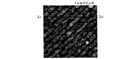
次いで、NiO薄膜を堆積させたサファイア単結晶基板を大気雰囲気下700℃で3時間アニールした。アニールされたNiO薄膜は、図1のAFM観察結果にみられるように、基板のステップ,テラスを反映して幅20nm,深さ約1nmの溝が約80nm間隔で平行に配列していた。断面プロフィルも、膜厚変動が最大でも1.0nmの範囲に収まっていた(図2)。
酸化物薄膜の超微細チャンネル構造が基板の原子ステップ高さ,テラス幅を反映していることは、素子/基板間の接続が良好であることを意味する。チャンネルは、基板の原子ステップの間隔に良く一致した間隔で、チャンネル方向も基板の原子ステップに一致していた。
【0016】
【実施例2】
実施例1と同じ条件下で用意したサファイア(0001)基板を用い、KrFエキシマレーザ(波長:248nm,パルス幅:約20ns)でYSZ(Y2O3を8.0モル%含有するZrO2)ターゲットを照射し、対向位置に配置されたサファイア(0001)基板上に膜厚約29nmのYSZ薄膜を700℃でエピタキシャル成長させた。成膜直後のYSZ薄膜の状態は、径30nmのナノ粒子が面内に並んだ平坦な膜面を呈し、約1nmのラフネスであった。
次いで、YSZ薄膜を堆積させたサファイア単結晶基板を大気雰囲気下1100℃で3時間アニールした。アニールされたYSZ薄膜は、図3のAFM観察結果にみられるように、基板のステップ,テラスを反映した周期的な溝をもつ超微細チャンネル構造をもち、膜厚変動も最大2.5nmと極僅かであった(図4)。
【0017】
【発明の効果】
以上に説明したように、原子レベルでステップ幅,テラス幅が制御された単結晶酸化物基板の平滑表面で酸化物薄膜をエピタキシャル成長させ、アニールすることにより、基板表面を倣って幅,深さが原子レベルで制御された溝をもつ超微細チャンネル構造が酸化物薄膜に作り込まれる。作製された酸化物薄膜は、素子/基板間の接続が極めて良好なことと相俟って、超微細化の要求が過酷な半導体素子,光学素子,超高感度センサ,超効率触媒,DNAデバイス,マイクロチップ媒体,燃料電池用等、広範な分野における超高機能素子として使用できる。
【図面の簡単な説明】
【図1】 実施例1で作製したNiO薄膜のAFM像
【図2】 同NiO薄膜の断面プロフィル
【図3】 実施例2で作製したYSZ薄膜のAFM像
【図4】 同YSZ薄膜の断面プロフィル[0001]
[Industrial application fields]
The present invention has a simple ultrafine channel structure expected to be used as a semiconductor element, light emitting element, sensor, catalyst, chemical reaction integrated microchip medium, DNA device carrier, and micro fuel cell element with extremely high sensitivity and efficiency. The present invention relates to a method of forming on a crystalline oxide substrate.
[0002]
[Prior art]
An insulating substrate such as a sapphire single crystal on which thin films having various functions are laminated is polished into a mirror state after a predetermined crystal plane is exposed on the surface in order to obtain a good bonding state to the functional thin film. The specific crystal plane is exposed to the substrate surface by adjusting the cutting angle when the single crystal substrate is cut with a diamond cutter or the like. The substrate after cutting is polished with diamond polishing powder, and then chemically etched in a liquid containing colloidal silica or the like. The mechanically and chemically polished single crystal substrate is mirror-finished in a very smooth state with a surface roughness of about 1 nm.
[0003]
When a normal semiconductor element is mounted, sufficient connection can be obtained even with a sapphire single crystal substrate mirror-finished by conventional mechanical polishing and chemical polishing. However, when targeting functional elements whose functions and density are rapidly advancing, satisfactory connection may not be obtained with a smooth surface that is mirror-finished by mechanical polishing or chemical polishing. For example, in a sapphire single crystal substrate on which a GaN blue light emitting element is mounted, the connection between the element and the substrate greatly affects the light emission output, and if the connection interface is disturbed, the output efficiency of blue light emission is lowered. In the SOS type (Silicon-On-Sapphire), satisfactory characteristics cannot be obtained if the silicon thin film / substrate interface is disturbed.
[0004]
[Problems to be solved by the invention]
Defects associated with higher functionality and higher density are caused by irregular irregularities on the surface of the single crystal substrate, exposure of different crystal surfaces, and the like. Specifically, a sapphire single crystal substrate that has been mirror-finished by mechanical polishing or chemical polishing is smoothed to a surface roughness of about 1 nm, but has no regularity in the uneven distribution. The observation result at the atomic level indicates that a different crystal plane having a crystal orientation other than the predetermined crystal plane is exposed on an uneven slope.
[0005]
When a thin film of silicon or the like is grown on a surface having irregular irregularities, crystal growth occurs in many irregularities, and the growth of many island crystals is promoted in the initial stage of growth. The island-like crystals grow while being interconnected with the progress of film formation, and as a result, crystal defects such as grain boundaries, edge dislocations, and helical dislocations are easily generated between the island-like crystals (JC Bean, Appl. Phys. Lett., 36 (1980) p.741-743). Crystal defects adversely affect the properties of the thin film formed on the substrate surface.
The different crystal plane exposed on the surface gives a growth orientation other than the epitaxial growth designed for the thin film grown on the crystal plane. Heterogeneous crystal planes are likely to appear on the slopes of the irregularities, and together with the growth of island-like crystals, it causes generation of different crystal grains at the interface. As a result, a complete single crystal thin film cannot be obtained, and the characteristics of the functional element deteriorate due to the disturbance of the interface.
[0006]
The present inventor found that the rearrangement of atoms on the sapphire single crystal surface differs for each crystal plane depending on the heat treatment conditions, and introduced surface smoothing by heat treatment instead of mirror finishing by conventional mechanical polishing and chemical polishing. (Patent No. 3015261). In the introduced method, the specific crystal plane is preferentially rearranged by selecting the heating temperature and heating time according to the crystal plane, and the atomic step height and terrace width of the sapphire single crystal substrate are controlled.
[0007]
[Means for Solving the Problems]
The present invention is a further development of the method introduced in Japanese Patent No. 3015261, in which a functional thin film is epitaxially grown by utilizing the surface structure of a sapphire single crystal substrate with controlled atomic step height and terrace width. Accordingly, an object is to obtain an ultrafine channel structure in which the groove width and groove depth are regulated at the atomic level.
[0008]
In order to achieve the object of the manufacturing method of the present invention, an oxide thin film or a nitride thin film is epitaxially grown on the surface of a single crystal oxide substrate whose step height and terrace width are controlled at an atomic level. An oxide thin film or nitride thin film is annealed in a high temperature atmosphere at 1550 ° C., and the oxide thin film or nitride near the step is formed so that a groove corresponding to the step of the single crystal oxide substrate is formed in the oxide thin film or nitride thin film. It is characterized by preferentially evaporating and diffusing material thin films.
For epitaxial growth of an oxide thin film or a nitride thin film, a vapor phase growth method, a laser MBE method, a sputtering method, a CVD method, a sol-gel method, an MBE method, or the like can be employed.
[0009]
[Operation and embodiment]
The present invention is directed to a single crystal oxide substrate having a smooth surface whose step height and terrace width are controlled at the atomic level. The atomic step height and terrace width are not limited to the method of Patent No. 3015261 in which the substrate is annealed at the heating temperature and heating time selected according to the plane orientation of the substrate, but hydrofluoric acid, sulfuric acid, phosphoric acid, etc. It can also be controlled by wet etching used or electrolytic etching that sweeps the applied potential. The single crystal oxide substrate is not limited to a sapphire single crystal, and TiO 2 (rutile), YSZ (yttria stable zirconia), SrTiO 3 , LaAlO 3, or the like can be used.
When an oxide thin film or nitride thin film is epitaxially grown on the surface of a single crystal oxide substrate whose atomic step height and terrace width are controlled, crystal nuclei are formed along the atomic level terraces and steps. Epitaxial growth reflecting the properties proceeds.
[0010]
The oxide thin film includes NiO, YSZ, TiO 2 , ITO, ZnO, SnO 2 , CuO, and the like, and the nitride thin film includes GaN, AlN, InN, etc., all of which are vapor phase epitaxy, laser MBE, sputtering, Epitaxial growth can be performed on a single crystal oxide substrate by a CVD method, a sol-gel method, an MBE method, or the like. In the case of epitaxial growth by vapor phase growth, 100 to 1000 nm / hour on a single crystal oxide substrate held at room temperature to 1000 ° C. in an oxygen or nitrogen atmosphere of 1.33 × 10 −6 to 1.33 × 10 1 Pa. Oxide or nitride is deposited at a film formation rate of
[0011]
Next, when a single crystal oxide substrate on which an oxide thin film or a nitride thin film is epitaxially grown is placed in a controlled atmosphere such as a vacuum, an inert gas, or an oxidizing atmosphere, and heated in a temperature range of 400 to 1550 ° C. for 10 minutes or more, Near the level step, disorder of crystal atom arrangement increases, and preferential evaporation and material diffusion occur locally. As a result, a nanoscale groove that follows the steps is formed. In order to promote local evaporation and material diffusion in the vicinity of the step, the heat treatment condition is set to 400 to 1550 ° C. × 10 minutes or more.
[0012]
The nanoscale groove formed by local evaporation and material diffusion separates the oxide thin film or nitride thin film on each terrace from each other, and an ultrafine channel structure appears. Since a nanoscale groove having a depth proportional to the thickness of the epitaxial thin film is formed, the depth of the nanoscale groove can be controlled by the thickness of the epitaxial thin film. In addition, since the groove follows the step shape, a nanoscale groove such as a straight line or a meandering shape can be shaped into various shapes. Furthermore, since the in-plane density of the groove is proportional to the density of atomic steps, it can be controlled by the off-angle of the crystal plane.
The fabricated ultrafine channel structure is used for chemical chips that use nanoscale grooves as flow paths, sensors that utilize uneven surfaces, catalysts, adsorbents, and the like.
[0013]
[Example 1]
The (0001) plane of the sapphire single crystal substrate whose surface was cleaned was heated in air to 1200 ° C. for 10 hours and then subjected to heat treatment for air cooling. As a result of AFM observation of the (0001) plane of the heat-treated sapphire single crystal substrate in the atmosphere, irregular irregularities were not detected, a terrace with a relatively wide area of about 80 nm in width, and an atomic step with a height of about 0.2 nm It was a very flat surface state in which atoms with a height were stacked one by one.
[0014]
Next, on a sapphire (0001) substrate at room temperature by a laser MBE method using a KrF excimer laser (wavelength: 248 nm, pulse width: about 20 ns) with an output of 1 J / cm 2 in an oxygen atmosphere of 1.33 × 10 −3 Pa. A NiO thin film having a film thickness of 25 nm was epitaxially grown at room temperature at a film formation rate of 100 nm / hour.
In the initial stage of epitaxial growth, the step shape of the substrate remained, but as the thickness increased, the film surface of the epitaxial thin film became an uneven surface imitating the step and terrace of the substrate. The roughness is a level of unevenness of about 1 nm, and the film surface has a high flatness as a whole.
[0015]
Next, the sapphire single crystal substrate on which the NiO thin film was deposited was annealed at 700 ° C. for 3 hours in an air atmosphere. In the annealed NiO thin film, as seen in the AFM observation result of FIG. 1, grooves having a width of 20 nm and a depth of about 1 nm were arranged in parallel at intervals of about 80 nm reflecting the step and terrace of the substrate. The cross-sectional profile was also within the range of 1.0 nm even when the film thickness variation was maximum (FIG. 2).
The fact that the ultrafine channel structure of the oxide thin film reflects the atomic step height and terrace width of the substrate means that the connection between the device and the substrate is good. The channel was well aligned with the atomic step spacing of the substrate, and the channel direction was also consistent with the atomic step of the substrate.
[0016]
[Example 2]
Using a sapphire (0001) substrate prepared under the same conditions as in Example 1, using a KrF excimer laser (wavelength: 248 nm, pulse width: about 20 ns), YSZ (ZrO 2 containing 8.0 mol% of Y 2 O 3 ) The target was irradiated, and a YSZ thin film having a film thickness of about 29 nm was epitaxially grown at 700 ° C. on a sapphire (0001) substrate disposed at the opposite position. The state of the YSZ thin film immediately after film formation was a flat film surface in which nanoparticles with a diameter of 30 nm were arranged in the plane, and had a roughness of about 1 nm.
Next, the sapphire single crystal substrate on which the YSZ thin film was deposited was annealed at 1100 ° C. for 3 hours in an air atmosphere. The annealed YSZ thin film has an ultra-fine channel structure with periodic grooves reflecting the steps and terraces of the substrate, as shown in the AFM observation result of FIG. Only a few (Fig. 4).
[0017]
【The invention's effect】
As described above, the oxide thin film is epitaxially grown on the smooth surface of the single crystal oxide substrate in which the step width and terrace width are controlled at the atomic level, and annealed so that the width and depth follow the substrate surface. An ultrafine channel structure with grooves controlled at the atomic level is built into the oxide thin film. The fabricated oxide thin film, combined with the extremely good connection between the element and the substrate, is a semiconductor element, optical element, ultra-sensitive sensor, ultra-efficient catalyst, DNA device, which are required to be extremely miniaturized. It can be used as an ultra-high performance element in a wide range of fields such as for microchip media and fuel cells.
[Brief description of the drawings]
1 is an AFM image of the NiO thin film prepared in Example 1. FIG. 2 is a cross-sectional profile of the NiO thin film. FIG. 3 is an AFM image of the YSZ thin film prepared in Example 2. FIG.
Claims (2)
Priority Applications (1)
| Application Number | Priority Date | Filing Date | Title |
|---|---|---|---|
| JP2003066951A JP3972011B2 (en) | 2003-03-12 | 2003-03-12 | Fabrication method of ultrafine channel structure |
Applications Claiming Priority (1)
| Application Number | Priority Date | Filing Date | Title |
|---|---|---|---|
| JP2003066951A JP3972011B2 (en) | 2003-03-12 | 2003-03-12 | Fabrication method of ultrafine channel structure |
Publications (2)
| Publication Number | Publication Date |
|---|---|
| JP2004276129A JP2004276129A (en) | 2004-10-07 |
| JP3972011B2 true JP3972011B2 (en) | 2007-09-05 |
Family
ID=33284711
Family Applications (1)
| Application Number | Title | Priority Date | Filing Date |
|---|---|---|---|
| JP2003066951A Expired - Fee Related JP3972011B2 (en) | 2003-03-12 | 2003-03-12 | Fabrication method of ultrafine channel structure |
Country Status (1)
| Country | Link |
|---|---|
| JP (1) | JP3972011B2 (en) |
Families Citing this family (1)
| Publication number | Priority date | Publication date | Assignee | Title |
|---|---|---|---|---|
| CN110893461B (en) * | 2019-11-06 | 2021-08-24 | 肇庆市华师大光电产业研究院 | Preparation method of nanoparticles with three-level composite structure |
-
2003
- 2003-03-12 JP JP2003066951A patent/JP3972011B2/en not_active Expired - Fee Related
Also Published As
| Publication number | Publication date |
|---|---|
| JP2004276129A (en) | 2004-10-07 |
Similar Documents
| Publication | Publication Date | Title |
|---|---|---|
| KR100607738B1 (en) | Electronic Device Substrate Structure and Electronic Device | |
| JP3813740B2 (en) | Substrates for electronic devices | |
| JP3950630B2 (en) | Fabrication of gallium nitride semiconductor layers by lateral growth from trench sidewalls. | |
| TWI411711B (en) | Process for selective masking of iii-n layers and for the preparation of free-standing iii-n layers or of devices, and products obtained thereby | |
| TWI286391B (en) | Substrate for growing gallium nitride, method for preparing substrate for growing gallium nitride and method for preparing gallium nitride substrate | |
| JP3966207B2 (en) | Semiconductor crystal manufacturing method and semiconductor light emitting device | |
| JP6083262B2 (en) | Laminated thin film with heteroepitaxial PN junction oxide thin film | |
| JP3662806B2 (en) | Method for manufacturing nitride-based semiconductor layer | |
| CN101473454B (en) | ZnO-based semiconductor element | |
| JP4651207B2 (en) | Semiconductor substrate and manufacturing method thereof | |
| JP3589200B2 (en) | Nitride semiconductor substrate, method of manufacturing the same, and nitride semiconductor device using the nitride semiconductor substrate | |
| JP4784609B2 (en) | Substrates for electronic devices | |
| JP4183787B2 (en) | Manufacturing method of substrate for electronic device | |
| US9190592B2 (en) | Thin film thermoelectric devices having favorable crystal tilt | |
| JPH0883802A (en) | Method for heat treatment of sapphire single-crystal substrate for improving surface characteristics | |
| JP2002293692A (en) | Single crystal sapphire substrate and heat treatment method for the same | |
| JP4557454B2 (en) | Single crystal sapphire substrate | |
| JP3972011B2 (en) | Fabrication method of ultrafine channel structure | |
| JPH04180219A (en) | Formation of crystal | |
| EP1589370A1 (en) | Optical deflection device, and manufacturing method thereof | |
| JPH11330569A (en) | Thermoelectric transducer and its manufacture | |
| JP2005260017A (en) | Forming method of ultrafine wire structure | |
| JP4014473B2 (en) | Method for manufacturing ultra-flat p-type oxide semiconductor NiO single crystal thin film | |
| JPS60193324A (en) | Manufacture of semiconductor substrate | |
| JP2008218981A (en) | Zinc oxide thin film |
Legal Events
| Date | Code | Title | Description |
|---|---|---|---|
| A621 | Written request for application examination |
Free format text: JAPANESE INTERMEDIATE CODE: A621 Effective date: 20041027 |
|
| RD02 | Notification of acceptance of power of attorney |
Free format text: JAPANESE INTERMEDIATE CODE: A7422 Effective date: 20070307 |
|
| RD04 | Notification of resignation of power of attorney |
Free format text: JAPANESE INTERMEDIATE CODE: A7424 Effective date: 20070309 |
|
| TRDD | Decision of grant or rejection written | ||
| A01 | Written decision to grant a patent or to grant a registration (utility model) |
Free format text: JAPANESE INTERMEDIATE CODE: A01 Effective date: 20070605 |
|
| A61 | First payment of annual fees (during grant procedure) |
Free format text: JAPANESE INTERMEDIATE CODE: A61 Effective date: 20070611 |
|
| R150 | Certificate of patent or registration of utility model |
Free format text: JAPANESE INTERMEDIATE CODE: R150 |
|
| FPAY | Renewal fee payment (event date is renewal date of database) |
Free format text: PAYMENT UNTIL: 20110615 Year of fee payment: 4 |
|
| LAPS | Cancellation because of no payment of annual fees |