JP3967800B2 - Signal processing device - Google Patents
Signal processing device Download PDFInfo
- Publication number
- JP3967800B2 JP3967800B2 JP25640197A JP25640197A JP3967800B2 JP 3967800 B2 JP3967800 B2 JP 3967800B2 JP 25640197 A JP25640197 A JP 25640197A JP 25640197 A JP25640197 A JP 25640197A JP 3967800 B2 JP3967800 B2 JP 3967800B2
- Authority
- JP
- Japan
- Prior art keywords
- signal
- phase
- output
- loop
- frequency
- Prior art date
- Legal status (The legal status is an assumption and is not a legal conclusion. Google has not performed a legal analysis and makes no representation as to the accuracy of the status listed.)
- Expired - Fee Related
Links
- 238000012545 processing Methods 0.000 title claims description 10
- 238000000034 method Methods 0.000 claims description 20
- 230000004044 response Effects 0.000 claims description 17
- 230000003044 adaptive effect Effects 0.000 claims description 13
- 238000001914 filtration Methods 0.000 claims description 3
- 238000012544 monitoring process Methods 0.000 claims description 3
- 230000011664 signaling Effects 0.000 claims description 3
- 230000010354 integration Effects 0.000 claims 1
- 239000003990 capacitor Substances 0.000 description 17
- 238000001514 detection method Methods 0.000 description 11
- 230000008569 process Effects 0.000 description 7
- 230000006978 adaptation Effects 0.000 description 5
- 230000003111 delayed effect Effects 0.000 description 5
- 230000036961 partial effect Effects 0.000 description 5
- 238000012360 testing method Methods 0.000 description 5
- 238000004891 communication Methods 0.000 description 4
- 238000013500 data storage Methods 0.000 description 4
- 238000010586 diagram Methods 0.000 description 4
- 238000011084 recovery Methods 0.000 description 4
- 238000012546 transfer Methods 0.000 description 4
- 230000008859 change Effects 0.000 description 3
- 230000033001 locomotion Effects 0.000 description 3
- 238000005070 sampling Methods 0.000 description 3
- 230000003595 spectral effect Effects 0.000 description 2
- 238000001228 spectrum Methods 0.000 description 2
- 230000003068 static effect Effects 0.000 description 2
- 230000007704 transition Effects 0.000 description 2
- 101100317039 Aedes aegypti VGA1 gene Proteins 0.000 description 1
- 238000007476 Maximum Likelihood Methods 0.000 description 1
- 238000013459 approach Methods 0.000 description 1
- 230000008901 benefit Effects 0.000 description 1
- 238000006243 chemical reaction Methods 0.000 description 1
- 238000012937 correction Methods 0.000 description 1
- 238000013144 data compression Methods 0.000 description 1
- 230000003247 decreasing effect Effects 0.000 description 1
- 238000013461 design Methods 0.000 description 1
- 230000000694 effects Effects 0.000 description 1
- 238000005516 engineering process Methods 0.000 description 1
- 239000000284 extract Substances 0.000 description 1
- 239000012467 final product Substances 0.000 description 1
- 238000004519 manufacturing process Methods 0.000 description 1
- 238000005259 measurement Methods 0.000 description 1
- 230000002829 reductive effect Effects 0.000 description 1
- 230000002441 reversible effect Effects 0.000 description 1
- 230000001360 synchronised effect Effects 0.000 description 1
- BWBONKHPVHMQHE-UHFFFAOYSA-N tiocarlide Chemical compound C1=CC(OCCC(C)C)=CC=C1NC(=S)NC1=CC=C(OCCC(C)C)C=C1 BWBONKHPVHMQHE-UHFFFAOYSA-N 0.000 description 1
- 238000012549 training Methods 0.000 description 1
- 230000001960 triggered effect Effects 0.000 description 1
Images


Classifications
-
- H—ELECTRICITY
- H03—ELECTRONIC CIRCUITRY
- H03L—AUTOMATIC CONTROL, STARTING, SYNCHRONISATION, OR STABILISATION OF GENERATORS OF ELECTRONIC OSCILLATIONS OR PULSES
- H03L7/00—Automatic control of frequency or phase; Synchronisation
- H03L7/06—Automatic control of frequency or phase; Synchronisation using a reference signal applied to a frequency- or phase-locked loop
- H03L7/08—Details of the phase-locked loop
- H03L7/14—Details of the phase-locked loop for assuring constant frequency when supply or correction voltages fail or are interrupted
-
- G—PHYSICS
- G11—INFORMATION STORAGE
- G11B—INFORMATION STORAGE BASED ON RELATIVE MOVEMENT BETWEEN RECORD CARRIER AND TRANSDUCER
- G11B20/00—Signal processing not specific to the method of recording or reproducing; Circuits therefor
- G11B20/10—Digital recording or reproducing
- G11B20/10009—Improvement or modification of read or write signals
- G11B20/10037—A/D conversion, D/A conversion, sampling, slicing and digital quantisation or adjusting parameters thereof
-
- G—PHYSICS
- G11—INFORMATION STORAGE
- G11B—INFORMATION STORAGE BASED ON RELATIVE MOVEMENT BETWEEN RECORD CARRIER AND TRANSDUCER
- G11B20/00—Signal processing not specific to the method of recording or reproducing; Circuits therefor
- G11B20/10—Digital recording or reproducing
- G11B20/10009—Improvement or modification of read or write signals
- G11B20/10046—Improvement or modification of read or write signals filtering or equalising, e.g. setting the tap weights of an FIR filter
- G11B20/10055—Improvement or modification of read or write signals filtering or equalising, e.g. setting the tap weights of an FIR filter using partial response filtering when writing the signal to the medium or reading it therefrom
-
- G—PHYSICS
- G11—INFORMATION STORAGE
- G11B—INFORMATION STORAGE BASED ON RELATIVE MOVEMENT BETWEEN RECORD CARRIER AND TRANSDUCER
- G11B20/00—Signal processing not specific to the method of recording or reproducing; Circuits therefor
- G11B20/10—Digital recording or reproducing
- G11B20/14—Digital recording or reproducing using self-clocking codes
- G11B20/1403—Digital recording or reproducing using self-clocking codes characterised by the use of two levels
-
- G—PHYSICS
- G11—INFORMATION STORAGE
- G11B—INFORMATION STORAGE BASED ON RELATIVE MOVEMENT BETWEEN RECORD CARRIER AND TRANSDUCER
- G11B20/00—Signal processing not specific to the method of recording or reproducing; Circuits therefor
- G11B20/10—Digital recording or reproducing
- G11B20/14—Digital recording or reproducing using self-clocking codes
- G11B20/1488—Digital recording or reproducing using self-clocking codes characterised by the use of three levels
- G11B20/1492—Digital recording or reproducing using self-clocking codes characterised by the use of three levels two levels are symmetric, in respect of the sign to the third level which is "zero"
-
- H—ELECTRICITY
- H03—ELECTRONIC CIRCUITRY
- H03L—AUTOMATIC CONTROL, STARTING, SYNCHRONISATION, OR STABILISATION OF GENERATORS OF ELECTRONIC OSCILLATIONS OR PULSES
- H03L7/00—Automatic control of frequency or phase; Synchronisation
- H03L7/06—Automatic control of frequency or phase; Synchronisation using a reference signal applied to a frequency- or phase-locked loop
- H03L7/08—Details of the phase-locked loop
- H03L7/14—Details of the phase-locked loop for assuring constant frequency when supply or correction voltages fail or are interrupted
- H03L7/146—Details of the phase-locked loop for assuring constant frequency when supply or correction voltages fail or are interrupted by using digital means for generating the oscillator control signal
-
- G—PHYSICS
- G11—INFORMATION STORAGE
- G11B—INFORMATION STORAGE BASED ON RELATIVE MOVEMENT BETWEEN RECORD CARRIER AND TRANSDUCER
- G11B20/00—Signal processing not specific to the method of recording or reproducing; Circuits therefor
- G11B20/10—Digital recording or reproducing
- G11B20/10009—Improvement or modification of read or write signals
-
- Y—GENERAL TAGGING OF NEW TECHNOLOGICAL DEVELOPMENTS; GENERAL TAGGING OF CROSS-SECTIONAL TECHNOLOGIES SPANNING OVER SEVERAL SECTIONS OF THE IPC; TECHNICAL SUBJECTS COVERED BY FORMER USPC CROSS-REFERENCE ART COLLECTIONS [XRACs] AND DIGESTS
- Y10—TECHNICAL SUBJECTS COVERED BY FORMER USPC
- Y10S—TECHNICAL SUBJECTS COVERED BY FORMER USPC CROSS-REFERENCE ART COLLECTIONS [XRACs] AND DIGESTS
- Y10S331/00—Oscillators
- Y10S331/02—Phase locked loop having lock indicating or detecting means
Description
【0001】
【発明の属する技術分野】
本発明は、データ処理装置および方法、並びに、接続に使用される電子回路に関し、特に、これに限定されるわけではないが、DDSデータ記憶システムを使用して、記憶されたデータを検索する装置および方法に関連する。また、本発明は、一般に、1又は複数の通信チャネルにおけるデータ処理の装置および方法に関する。
【0002】
【従来の技術】
特に、ISO11EC標準12247で定義されたDDS(デジタル・データ記憶)手段によって、コンピュータ・データのような、大容量のディジタル・データを確実に記憶し検索する装置を提供することが、既に知られている。
【0003】
上記のフォーマットを使用するDDS読出し/書込み装置において、データは、1又は複数の電気磁気ヘッドを備える回転ドラムによって、磁気媒体でコーティングされたテープから成る細長い記録媒体上に記録される。テープは、2つのスプールまたはリール間に渡るパスに沿って、モータ駆動キャプスタンによって動かされ、部分的にドラムのまわりを巻く。ドラムのヘッドの回転面は、テープの移動面に対してある角度をなして配置されているので、各ヘッドは、中心線に対してある角度でテープの幅を横切って延びる連続したトラックに沿ってテープを横切る。この装置は、テープ上へ記録するに適した誤り検出訂正コードを含む信号にデータをエンコードする回路を含み、記録媒体の特性に最も適した形にそれらの信号を調整する回路を含む。データ検索のために、テープ上に記憶された磁界変化を検出し、次の処理にふさわしい形式にそれらの信号を調整して対応する信号を誘導し、エンコードされたデータをデコードして、エラーを検出し訂正するために付加的な回路が備えられる。
【0004】
現在のフォーマット(DDS−2)において、データは、1インチにつきおよそ61キロビット(kbpi)(1センチメートルにつきおよそ24キロビット)のビット密度で記録される。このビット密度で、典型的なDDSテープ・カートリッジは、最も長く使用可能なテープと、テープが収容することができるデータ量を最大にするデータ圧縮のような技術を使用して、およそ8ギガバイト以上のデータを、現在記憶することができる。コンピュータ装置の使用が絶え間なく増加し、そのような装置によって処理され記憶されるデータ容量が増加するに従って、さらに、DDSテープ・カートリッジの容量を増やすことが望まれるようになった。
【0005】
我々は、線形記憶密度を2倍にし、ユーザ・データのために使用できる記録トラックの割合を増やすことによって、さらに記憶容量を増やす新しいフォーマット(DDS−3)を開発するプロセスにある。これとともに、これらの改良は、与えられたテープ長さのカートリッジに対して、DDS−2のデータ容量の約3倍の容量を提供すると予測されている。DDS−3フォーマットは、最も長く実行可能なテープ上に記録するとき、12ギガバイトの圧縮されていないユーザ・データか、または一般的に24ギガバイトの圧縮されたユーザ・データの記憶容量を提供するように設計される。
【0006】
この方式の詳細は我々の以前に発表された国際特許出願WO95/15551によって示され、その特許出願の内容は、ここで参照されて取り入れられている。
【0007】
DDS−3の線形ビット密度がDDS−2の2倍であるため、テープの上のビット間隔は、好ましい読取りヘッドのギャップのおよそ半分である。このことは、読取りヘッドからの出力信号が、2つの離れたレベル(+1、−1)の間で変化する代わりに、3つのレベル(+2、0、−2)の間で変化し、即ち、DDS−3は、3レベル・システムであることを意味する。
【0008】
部分応答最大確度(PRML:Partial Response Maximum-Likelihood)データ回復チャネルの使用によって、記録されたデータを回復することが提案されている。
【0009】
「部分応答」とは、検出回路入力で決定性符号間干渉を強制することによって、データ転送のためにナイキスト周波数バンド幅までを必要とするだけの、実行可能な部分応答信号方式を示す。その一例は、離散的時間伝達関数F(D)=D+1によって示される、PR−1(または対2進(duobinary))部分応答システム(記録チャネル伝達関数)である。他の例として、クラスIVやPR−4のようなものが存在し、これらの可能性を除くものではない。
【0010】
「最大確度」とは、1度にちょうど1つの受取られたサンプルの代わりに、受取られたサンプルのシーケンスを使用する出力データの最も適当なシーケンスを選択するヴィテルビ・アルゴリズムを実行する、最大確度検出デコーディング方式を示す。
【0011】
DDS‐3の一般に提唱される方式の読取りモードにおいて、ほぼ等化された信号が受取られて自動利得制御(AGC)にかけられ、信号振幅が確立され安定させられ、次いで完全な適応性等化(Adaptive Equalisation)にかけられ組み合わされたPRー1ターゲットになる。適応性等化ステップにおいて、適応性のサンプルされた有限インパルス応答フィルタが、3レベルPR‐1ターゲット伝達関数を提供するために使用される。一実施例において、適応性等化の後、信号は、アナログからデジタルへ変換され、3レベル・ヴィテルビ(Viterbi)(すなわち最大確度)検出が続く。これを実行するために、クロック情報は、入力信号から抽出されて、適応性イコライザ、アナログ/デジタル変換器、およびヴィテルビ・デコーダを同期させるために使用される。他の実施例において、アナログ/デジタル変換の後で、適応性等化が代わりに実行される場合がある。
【0012】
以前のDDSフォーマットにおける同様に、提案されたDDS−3フォーマットにおいても、データは、交互のアジマス(azimuth)の一連のトラック(それぞれAトラックおよびBトラックと呼ばれる)として記憶される。各トラックのそれぞれの端は、消耗してもよいマージン領域で占められ、フロント・マージンの後にしばしばそのマージンから区別がつかないプリアンブル領域が続く。プリアンブル領域は、通常単純な正弦波のトーンであり、データを全く運ばないが、AGCループとクロック回復ループが速いロック・オンを達成するのを可能にし、さらに、メイン・データ領域の始まりを識別するために存在する。プリアンブル検出回路は、適応性イコライザを制御してチャネルがプリアンブルやマージン領域を適応化しないようにする。こうしないと、チャネルがデータ部分について最適化されないからである。
【0013】
この明細書において、通信チャネルの用語は、記録媒体から読み取られるデータのチャネルを含む広い意味で使用される。
【0014】
【発明が解決しようとする課題】
DDSデータ読み取りシステムは、いろいろな異なる条件下で、読み取り波形からビット・クロックを回復させることを位相同期ループ(PLL)に要求する。例えば、フィードフォーワド・イコライザ(FFE:Feed Forward Equalizer)、アナログ/デジタル変換器、およびヴィテルビ・デコーダのような他の構成装置を駆動するために使用されるので、回復された読み取りクロックは、強力でなければならない。本質的に、PLLは周波数と位相同期をトラックのはじめで獲得しなければならず、許容できる位相エラーでヘッド・テープ速度ジッタによって生じるビット周波数変動がこれに続く。
【0015】
DDS−2フォーマットにおいて、テープの読取りは、ビット・サンプリング時間がアイ・センタ(eye centre)にある2レベルの信号になる。従って、この方法が振幅変動に比較的無感応なので、PLLの位相検出器は、典型的にはゼロ交差をテストすることができる。
【0016】
我々の提案するDDS−3フォーマットにおいて、テープの読取りは、3レベルのPR−1信号になる。この場合、位相検出器は、入力信号の大きな部分を不適合にすることなく、単純なゼロ交差のテストをすることができない。従って、我々は、公称信号レベルの約半分、即ち、公称+2、0、−2のレベル信号について+1、−1で、閾値を有する閾値交差方式を使用する。
【0017】
我々は、テープ・ドロップアウトのような一定の状況で、PLLがロックを失うことがあることを見いだした。
【0018】
【課題を解決するための手段】
従って、我々は、この条件またはこの条件になる状況をモニタし、条件が検出された場合、周波数をデフォルト値にリセットするシステムを設計した。また、この状況は、記録された媒体から導かれるもの以外の通信チャネルのタイプに広く適用できる。
【0019】
この発明の一面において、ビット・レートに変動を有する信号を処理する装置が提供され、この装置は、前記信号からビット・クロックを回復させる位相同期ループ手段と、前記位相同期ループ手段がそのロックを失うか、悪い条件が検出されるとき、前記位相同期ループの出力周波数を予め設定した値にリセットする手段と、を含む。
【0020】
いろいろな条件が周波数の再設定をトリガするために使用されうる。例えば、周波数が、予め設定された許容バンドの外側に変化した場合、それはリセットされる。または、信号がFIRフィルタか同様のものによって適応的にフィルタされる場合、デジタル・フィルタの係数がモニタされ、これらの係数がお粗末なSNR比を推測させるときPLLの周波数がリセットされる。
【0021】
ここで参照するように、FFEシステムは、キック・スタート・ルーチンを含み、フィルタ係数の反対のセットの始まりは、FFEのフィルタ係数のリセットと、PLLのデフォルト周波数のセットの両方のトリガに使用される。
【0022】
さらに、信号に自動利得制御がかけられる場合、利得制御信号の大きさがモニタされ、これが、予め設定された範囲から離れるか、異常に低いSNRを示す傾向がある閾値を渡すならば、この条件は、PLL周波数をリセットするために使用される。
【0023】
【発明の実施の形態】
ここに記載されているデータ記憶装置は、DATC協会規格(1987年6月、日本電子機械工業会(東京(日本)))に従うPCM音声データの記憶装置に使用されるフォーマットと同様のフォーマットで、記録テープ上の斜めのトラックにデータを記憶するらせん走査技術を利用する。しかしながら、本発明の装置は、ディジタル化された音声情報よりもむしろコンピュータのデータを記憶するのに適用される。従来同様に、この装置は、ヘッド・ドラムが回転しているとき、磁気テープが所定の角度で回転ヘッド・ドラムを横切るらせん走査テープ・デッキを含む。ヘッド・ドラムは、直径に関して向かい合った一対の読取りヘッドと、読取りヘッドと90度の位置に、直径に関して向かい合った一対の書込みヘッドを収納する。従来同様に、これらのヘッドは、テープを横切って斜めの重なるトラックに書き込む。1つのヘッドで書き込まれるトラックは、正のアジマスを有し、もう一つのヘッドで書き込まれるトラックは、負のアジマスを有する。
【0024】
トラックは、装置に提供されるデータ(メイン・データ)およびサブ・コードとして知られている補助情報の項目を記憶するために使用され、このサブ・コードは、例えば、メイン・データの論理的な構成、テープ上の配置、一定の記録パラメータ(フォーマット識別子やテープ・パラメータなど)、およびテープ使用ヒストリに関連する。また、トラックは、データ・バイト境界を識別することを可能にする同期バイト(sync bytes)を含み、この同期バイトは、テープ移動などを制御するタイミング信号を生成するために使用される。各々のトラックの始めと終わりにはマージン領域があり、始めのマージンとメイン・データ領域の間にプリアンブル・ブロックがある。
【0025】
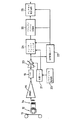
図1において、テープ10上に記憶されたデータは、メイン・ドラム上の読取りヘッド12によって読取られ、信号は回転変圧器14を通して増幅器16に渡され、そこからフィルタ18に渡され、組み合わされたPR−1ターゲットに初期近似等化される。実際上、一端をアースするのではなくむしろ読取りヘッドから差動信号が受け取られる。しかし、図1は、1つの信号ラインのみを表示している。それから、信号は、自動利得制御(AGC)回路20に供給され、フィルタおよび積分回路18から受取った3レベル信号の+2と−2の振幅を確立して安定させる。AGC回路20からの信号は、クロック信号を回復する位相同期ループ(PLL)22に供給され、更に、結合されたPR−1ターゲットへの適応性等化を提供するフィードフォーワド・イコライザ(FFE)24として記載される適応フィルタに渡されるので、、全チャネル周波数応答が、理想的なPR‐1の部分応答チャネルの特性と一致する。フィルタされた信号は、アナログ/デジタル変換器(ADC)26に供給され、フィルタされた信号のディジタル化されたバージョンとなり、ヴィテルビ検出回路28へ供給される。ヴィテルビ検出回路28の出力は、NRZI−エンコードされたデータ・ストリームである。他の実施例において、フィードフォーワド・イコライザ24は、アナログ/デジタル変換器の前でなくて後に設置される。
【0026】
図2において、自動利得制御システムは、より詳細に示され、2つの差動信号ラインが明白になる。
【0027】
動作時、自動利得制御システムは、指定された公称振幅の範囲内で、FFE24に一定の信号振幅を与えるのに役立つ。理想的な動作のために、この振幅は、1つのトラックの長さに沿って、または、同じアジマスのトラック間で変化してはならない。指定された絶対利得エラーの境界内では、信号振幅は、それが実質的に一定である限り、大きさは重要なことではない。AGC制御ループのどのような一時的な動作の間でも、VGA32の振幅の変動は、絶対利得エラーより非常に小さい予めセットされた相対利得エラーの範囲内に制御されなければならない。記録されたトラックは、異なるスペクトル特性の帯域を含む。これらの帯域の最も重要なものは、プリアンブル領域とランダム・データ領域である。AGCブロック20の理想的なオペレーションの流れのために、AGCシステムは、全体としては、周波数スペクトルの変化に対して免疫がなければならない。プリアンブル領域とランダム・データ領域の間の境界のいずれの側でも、相対振幅許容範囲を越えてはならない。
【0028】
信号が、ライン30上で電圧利得増幅器(VGA)32に入力され、出力は、出力ドライバ34を通過して、前方のADC26またはFFE28(図2で示さず)に渡される。増幅器38、ローパスフィルタ40、およびサマー(合算器、summer)42を有するフィードバック・ループ36が、DCオフセット制御のために用意されている。また、出力ドライバ34からの出力は、出力信号のピークを検出する共通の簡単なピーク検出器44に渡される。ピーク検出器44の出力は、デジタル/アナログ変換器(DAC)46からのターゲット値と共に、比較回路として働く演算相互コンダクタンス増幅器(OTA:operational trans-conductance amplifier)48(VGA制御電圧)に供給される。
【0029】
増幅器48の出力(VGA制御電圧)は、VGA32に利得制御信号を供給する利得制御回路50に供給される。ピーク検出回路44、増幅器48、および利得制御回路50によって定義される利得制御ループは、比較的速い応答時間を有する。
【0030】
また、増幅器48の出力は、プリアンプ52とラッチング比較器54に供給され、ラッチング比較器54は、プリアンブル領域とメイン・データ領域の間のインタフェースでまたはその直前で、VGA制御電圧のメジャーVGA1を追跡し、それを保持する。VGA制御電圧の第2のメジャーVGA2は、いくつかのチャネル・ビットの後に(すなわち、メイン・データ領域の初めで)取られる。VGA1とVGA2の直接の比較によって、電圧利得アンプ32の利得は、プリアンブル領域とランダム・データ領域の間で転移する際に、増加したのか減少したのかを示す。この情報に基づいて、該当するAまたはBトラックのピーク検出器のプリアンブル・ターゲットを保持している該当するカウンタ60または62は、増やされるか減らされる。プリアンブル・ターゲットの調整は、ライン64を通して可能にされ、また不可能にされる。レジスタ65は、全ての条件下でのピーク検出器44についてのランダム・データ・ターゲットに対する定数値を保持する。ターゲット制御ループの応答は、利得制御ループより遅い。
【0031】
初期トレーニング期間後、プリアンブル・ターゲットは、プリアンブル領域とメイン・データ領域の間のインタフェースの直前とその後で、VGA制御電圧を等化するよう適応している。これは、次のトラックのために用意されてカウンタ60と62に保持されるそれぞれのターゲット値を持つAおよびBトラックについて別々にになされる。
【0032】
したがって、この回路において、プリアンブルとランダム・データに対する単純なピーク検出器44の異なる応答は、適応的に調整される。プリアンブル・ターゲット・カウンタ60と62は、オーバーフローやアンダーフローをしない飽和カウンタである。したがって、1つが、現在その最大カウントを保持し、更に増加することを要求されるならば、それはその最大カウントを維持する。同様に、それがその最小のカウントを保持しているとき、更に減らすように要求されるならば、それは最小のカウントを維持する。
【0033】
ターゲット制御ループのバンド幅や応答時間は、ライン51でOTA増幅器48のバンド幅モードを調節することによって、予め設定した値の間で調節される。AおよびBのトラックのプリアンブル領域は、クロック回復ループとAGCループが、既知の特性のデータ上で速いロックアップを達成するのを可能にするために存在し、したがってそのような領域は短い。
【0034】
AGCシステムのバンド幅は、この速いロックアップを容易にするために、プリアンブル領域の開始で高いように選択される。大まかな振幅調整が達成されたならば、正確な利得振幅調整が達成されるまで、媒体バンド幅モードをライン51で選択することができる。それから、VGA制御電圧による過度の信号の変調を避けるために、ランダム・データの到着に先立ち低帯域幅モードが選択される。
【0035】
この配列によって、利得は、下流を処理するに十分正確に制御することができる。
【0036】
図3を参照すると、AGCブロック20を通過した後、信号は、FFE24に加えられる。FFE 24は、有限インパルス応答(FIR)フィルタ66と、係数コンデンサ69のバンク68と、回路70を有する。回路70は、ライン72上の出力と基準ジェネレータ74によって生成された基準値との間のエラーを減らすために係数を適応させる。
【0037】
AGCブロック20からの信号は、入力の連続的に遅らされたバージョンを同時に生成する遅延78をもつタップ付き遅延線76上のFIRフィルタ66へ入力される。FFE24内の回路構成の大多数は、スイッチ・コンデンサ技術で実行される。FIRフィルタ66の76での入力は、位相ロックループ(PLL)22によって決定されるクロック・タイムでコンデンサを充電することによって、サンプルされる。それから、この電荷は、遅延線を形成するビット時間に1つのコンデンサから他のコンデンサに渡される。
【0038】
遅延線に沿った各段の出力は、乗算器79で、関連する係数コンデンサ69からのそれぞれの加重係数で乗算され、全ての加重出力は、サマー80によって合計され、ライン72上にフィルタ・デジタル出力を提供する。
【0039】
レジスタ68の係数は、位相ロックループ22によって定義されるようなビット・サンプリング時間で、ライン72上の等化されたアナログ信号のSN比(SNR)を最大にするよう繰り返して適応される。一方、ヘッドとテープの周波数応答またはヘッドとテープの接触条件は変化する(製造中のまたは動作中のどちらでも)。 DDS−3モードにおいて、PR−1入力信号は、フィルタ18によって、通常、スペクトルで形成され、3つのレベル(+2、0、−2)から成る。この場合、適応ブロック70において、係数は、平均最小二乗(LMS)アルゴリズムで適応させられる。その場合、基準ジェネレータ74によって提供される最も近い3レベル公称信号レベルとFIRフィルタ出力との差であるエラー信号を使用する。エラー信号は、分岐され遅延された入力信号と共に、それぞれの乗算器82に並列に供給され、これは、係数コンデンサ69に各係数を適応させるために使用される。
【0040】
DDS−3モードにおいて、等化された信号は、それが基準ジェネレータ74からの基準値を使用する+2、0、または−2の信号であると考えられるかどうかを判断するために決定ブロック84でモニタされる。基準ジェネレータ74は、信号が+2、0、または−2のいずれかであるかを決定するために決定ブロック84が使用するプラスマイナス1のスライス・レベル信号を供給する。次いで決定ブロックは、基準ジェネレータ74に、適当な+2、0、−2の公称レベルをエラー・サマー75に供給させる。エラー・サマー75は、フィルタ出力信号をも受取り乗算器82に供給されるエラー信号を得る。適応のレートは、乗算器86、88で、信号(μsig)とDC係数(μdc)についての予め設定した値(一般的に6)の間で変化する。
【0041】
FFE24は、ランダムなデータ領域に対して最適の係数セットからすぐにはずれて適応するので、AおよびBデータ・トラックのプリアンブルまたはマージン領域に適応することを許されてはならない。メイン・データ領域の開始と終了は、テープ上のデータの構造と読込まれるフォーマットの知識に基づき、とりわけプレアンブル検出器23(図1)に依存して、タイミングとインテリジェントな決定の組合せを使用するデータ回復状態マシーンによって、通常予測される。プリアンブル検出回路23は、従来のタイプのものでよく、典型的にはプリアンブル領域の純粋な正弦波のトーンにマッチした整合フィルタの形であってよい。それは、信号が特徴のある正弦波のトーンを含む時、高い出力を供給する。プリアンブル検出回路23の出力は、状態マシーン21に供給され、状態マシーンは、AおよびBプリアンブルとAGC20におけるメイン・データ・ターゲットについてターゲット切り替えを制御し、フィードフォーワド・イコライザ24におけるAおよびBトラック係数の選択をも制御する。
【0042】
AおよびBトラックのスペクトル特性は相違し、コンデンサ69は、AおよびBトラックに対する別々の係数を記憶し、適当なセットの係数が各トラックの始めでFFEコンデンサ69に書き込まれる。
【0043】
この装置は、係数コンデンサ69に対応する一組の係数レジスタ(図示せず)を含む。コンデンサ69で保持された値は、A/Dコンバータによって処理され、係数レジスタに記憶される。各トラックの始めで係数を回復するために、それらは、デジタル時間ログ・コンバータによって処理され、コンデンサに供給される。したがって、典型的な順序は、次のようになる。
1. A係数レジスタの内容がFFE係数コンデンサ69に書き込まれる。
2. FFEは、ブロック70によって実行される適応処理に従って、Aトラック上にこれらの係数を適応させる。
3. 適応されたFFE係数コンデンサ69の値がディジタル化され、A係数レジスタに記憶され、B係数レジスタの内容がFFE係数コンデンサ69に書き込まれる。
4. FFEは、ブロック70によって実行された適応処理に従って、Bトラック上にこれらの係数を適応する。
5. Bトラックの適応されたFFE係数コンデンサ69の値がディジタル化されて、B係数レジスタに記憶される。
【0044】
しかしながら、いろいろな他のルーチンが続いてもよい。例えば、そのアジマスの前のトラックの終わりで適応された係数値にかかわりなく、各トラックが、トラックの始めで係数コンデンサへロードされる係数のそれ自身の標準セットを有することがありえる。または、係数コンデンサは、そのアジマスの前のトラックを介する途中の一部で受け取られ適応された値をロードされてもよい。係数がとられる位置は、最高の適応を提供するための機械条件に従って最適化される。例えば、トラックが曲っている場合、トラックに沿っておよそ途中の半分から係数をとることがベストとなる。あらゆる機械の設計で、最適な位置は経験的に決定され、そして、製品化される機械は、この地点で係数をとるようにプログラムされる。AおよびB係数を異なるポイントでとることができる。
【0045】
したがって、前のAトラックについての読取り動作の最小のエラー部分からの適応されたフィルタ係数は、次のAトラックの係数の初期セットとして使用することができ、そして、同様の処理がBトラック係数に適用される。トラック終わりの非線形に迷い込むのを避けるために、読取り動作の最小エラー部分の開始の後、あらかじめ決められた時間に係数値をとるために「スナップショット・タイマ」方式を使用することがえきる。
【0046】
一実施例において、所与のAまたはBトラックの係数の連続したセットを多くのトラックにわたって平均して、次のAまたはBトラックのための係数の初期セットとして、使用することができる。これは、1トラックでは素早く適応させることができ、多重トラックでは遅いという利点がある。これは、デジタル方式で最も容易に実施することができる。
【0047】
特別な例として、AおよびBトラック係数セットのそれぞれにおいて、13の信号の係数と1つのDC係数がある。
【0048】
もし、FFE24が、読取り信号でドロップ・アウトに対抗する間、適応しているならば、FFE係数は、回復することができない状態に誤って適応することがある。これに対抗するために、自動再始動装置が組み込まれる。中心係数がプログラム可能な閾値(例えば50%)の下に落ちると、その係数は全て、デフォルト・セットの値に強制される。例えば、中心信号係数に1単位の値がロードされるときの単位ステップのインパルス応答および残りの信号係数は、ゼロに強制される。この開始位置から、FFE24は適応し続けることを許される。それは、再び誤って適応するならば処理が自動的に繰り返されるか、または、ドロップ・アウトが回復可能な信号を含むならば、互いに正しい目標値に近づく。
【0049】
したがって、図に示した実施例において、中心係数は、それを基準ジェネレータ91からのプリセット基準値と比較する比較回路90に供給され、そして、もし、実際問題として、中心係数が、不正確な状態で安定した係数になるような値以下に落ちた場合、係数のデフォルト・セットを強制する「キック・スタート」ルーチンを実行する。
【0050】
トラック交差モードにおいて、テープの上のトラックが読取りヘッドの走査パスと整合しないとき、ヘッド出力信号は、1走査につき何回も良/不良のSNRの間を循環し、この状況において、図3の方式は、回復されるデータ量を増やすことができる。
【0051】
FFE係数の多数の安定した、適応された状態が可能であるが、これらうちの小さなセットだけがこの方式に有用である点に留意する必要がある。上述された技術は、中心係数だけをテストしており、全ての可能な望ましくない状態を検出することができるというわけでない。しかしながら、この技術は、この中心係数に加えて、またはこれに代えて他の係数をモニタするように拡張することができ、また、係数の異なるデフォルト・セットを強制することができる。また、それを一つの限度でなく範囲として、モニタすることができる。
【0052】
ここで図4を参照すると、位相同期ループ22は、いろいろな異なる条件で、読み取り波形からビット・クロックを回復させることを要求される。本質的に、位相ロックループ22は、周波数と位相同期をトラックの最初で獲得しなければならず、許容できる位相エラーで、ヘッド・テープ速度ジッタに起因するビット周波数変動に追従しなければならない。
【0053】
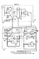
幅広いアウトラインにおいて、位相同期ループ22は、位相検出器92、ループ・フィルタ94、および位相アキュムレータ96を有する。位相アキュムレータ96の出力は、システム・クロック・タップ付き遅延線98から得られる一連のクロック信号から適当なクロック信号を選択するために使用される。
【0054】
入力信号が、AGC20で自動利得制御にかけられるので、公称レベルが、2、0、−2の単位となる。2つの入力比較回路100、102は、入力信号が+/−1単位(近似)閾値を横切る時間を捜す。そして、これらの閾値交差の時間は、位相エラーを決定するために現在のクロック・タイム(システム読取りクロック)と比較される。位相エラーは、デジタル(すなわち、位相エラーの符号と大きさに従い、−4、−3、−2、−1、1、2、3、4)でエンコードされて、ループ・フィルタ94に渡される。
【0055】
ループ・フィルタ94で、(デジタルの)位相エラーは、2つの乗算器104、106とアキュムレータを使用してフィルタされる。上位フィルタリング・パスで、位相エラーは、定数(Kp)を掛られる。下位フィルタリング・パスで、位相エラーは、定数Kiを掛けられ、その結果は、Kiアキュムレータ108によって累算される。累算された(Ki)結果と直接の(Kp)結果は、一緒にサマー110で加えられて、位相アキュムレータ96に渡される。
【0056】
位相アキュムレータ96は、ループ・フィルタ94の出力を積分する。位相アキュムレータ出力の上位4ビットが、「ポインタ」の働きをする。このポインタは、遅延線98で得られる外部のシステム・クロックの16の遅延バージョンのうちのどれが、システム読取りクロック(すなわち、入力信号に同期されたクロック)として使用されるかを示す。
【0057】
したがって、入力信号がシステム読取りクロックと位相外れになるにつれて、位相エラーがループ・フィルタ94の出力で大きな値になり、それによって、位相アキュムレータ96がインクリメントし、結局その出力の上位4ビットを変更する。これによって、入力信号の位相により近いシステム・クロックの遅延バージョンが選択される。
【0058】
本方式のより細部を参照すると、最終製品における誤り率を最適化するためにループ・フィルタ・パラメータは、プログラム可能であり、第2順位のループが仮定される。更に、ループのバンド幅は、2つの前もってプログラムされた値の間で、リアルタイムでスイッチ可能である。これは、プリアンブル・ゾーンを最も有効に利用するためであり、データ領域で低い位相ジッタを維持する。位相同期ループ22は、トラックの通常のリプレイの間に発生する信号ドロップ・アウトの後、位相同期を回復させることができなければならない。
【0059】
回復させられた読取りクロックは、FFE24、ADC26およびヴィテルビ・デコーダ28を駆動するので、強力でなければならない。位相同期ループ22は、DDS−1/2またはDD−3のフォーマットで稼働ができることが好ましい。DDS−1または2のフォーマットは、ビット・サンプリング時間がアイ・センタにあるとき2レベルの信号になる。ここで、この方法は単純で振幅変動に比較的無感応であるので、位相検出器92は、典型的にゼロ交差のテストをする。
【0060】
DDS−3フォーマットで、フォーマットの読取りは、3レベルのPR−1信号になる。この場合、位相検出器92は、入力信号の大きな部分を不合格とすることなく、単純なゼロ交差のテストをすることができない。閾値交差方式が必要とされる(およそ+1、−1)。
【0061】
したがって、PLL22は閾値交差時間位相検出器92を含み、その出力は、離散的なステップに量子化される。DDS−1または2のモードで、位相検出器は、ゼロ交差に応答するが、DDS−3モードでは、2分の1公称信号レベル交差に応答する。
【0062】
図4は、位相検出器92を介す2つの(概念上の)パスを示す。ここで、入力信号(AGC20から)は、100、102で、半分の公称信号レベル閾値レベル(正および負)のそれぞれと比較される。入力信号の中の閾値交差のタイミングは、比較回路出力サンプラ116で、(16のタップ付き遅延線98から誘導された)出力クロックの(1/8の期間でシフトされた)8つの均一に区切られた位相と比較される。そして、ループ位相エンコーダ118で、現在の出力位相選択と比較される。量子化された位相は、入力交差が落す8つの出力クロック位相の間から、ループ位相セレクタ120によって直接判断される。
【0063】
DDS−1または2のモードで、入力信号は、単一の公称ゼロ・レベル基準値と比較され、図4の上位(概念上の)信号パスのみが使用される。DDS−3モードで、半分の公称信号閾値は、位相検出器閾値基準レジスタ112、114から誘導される。これらのレジスタは、DAC基準値をAGCランダム・データ・ターゲットDAC基準値にプログラムする。この方式は、AGCターゲットおよびPLL位相検出器が独立して最適化されることを可能にする。
【0064】
ループ位相セレクタ120からの量子化された位相出力は、Kp(比例項)とKi(積分)項を有するデジタル・ループ・フィルタ94に供給される。図において、位相検出器92の出力は、(状態(−4、−3、−2、−1、0、1、2、3、4)をエンコードする)4ビット・バスととして、また、乗算器104、106の出力は、8ビット・バスとして表示される。
【0065】
KpとKi乗数は、一般的に以下の範囲を有することができる。
【0066】
【数1】
Kpの範囲 = 0............31
Kiの範囲 = 0............31
乗算器出力 = −124..........124
【0067】
Ki乗算器106は、この例では以下の範囲を有するKiアキュムレータ108に、データを渡す。
【0068】
【数2】
Kiアキュムレータ・ビット = 12
Kiアキュムレータ範囲 = −2048...........2047
【0069】
Kiアキュムレータ108は、入力Ki乗算器出力を積分するが、アキュムレータからの最上位8ビットが、110でKp乗算器104からの8ビットに加えられ、位相アキュムレータ96の(最下位)エンドに供給される。
【0070】
したがって、ループ・フィルタ94は、ビット周期毎に、位相アキュムレータ96へ、−252........252を供給することができる。KpおよびKi値の2つのプログラム可能な対がレジスタ105、107で得られ、ループに速いまたは遅い時間定数を与える。この定数は、システム要求に従って状態マシーンによって選択される。
【0071】
Kiアキュムレータ108は、位相同期を失うかまたはその危険にあることが示されるとき再プログラム可能なように構成される。例えば、プリアンブル領域においてPLL周波数が初期化される場合がある。いわゆる「スタント・モード(stunt modes)」の間、速い前進テープ運動のために、Aトラックの中心周波数が低くされ、Bトラックの中心周波数が高くされる(逆テープ運動ではその逆になる)とき、周波数オフセットが発生する。更に、Kiアキュムレータ108が正または負にオーバーフローし、中心周波数が許容範囲外にあることを示すことがある。さらにまた、上述のFFE係数「キック・スタート」ルーチンがトリガーされるならば、Kiアキュムレータ108は再び中心付けされてもよい。この状態は、テープ・ドロップ・アウトまたは信号に対してその他の障害が存在し、PLLがその位相同期を失いそうであることを示唆することを示す。
【0072】
これらの状態で、Kiアキュムレータ108の最上位ビットは、可変位相発振器周波数オフセット・レジスタ109の内容をロードされ、これにより周波数がデフォルト値に中心づけられる。例えば、周波数は、PLL22が現在のトラックを読み始めた周波数に再び中心づけられてもよい。
【0073】
デジタル位相アキュムレータ96は、ループ・フィルタ94の出力を合計し、4つの最上位ビットを使用して16のタップ付き遅延線98から出力クロック位相を選択する。この遅延線98は、それ自身、システム・ビット周波数クロックに位相ロックされている。また、この遅延線98からの16のシステム・クロック位相は、位相検出器92の比較回路出力サンプラ116によって、閾値交差のタイミングを実行するために使用される。ループ・フィルタ・アキュムレータ108から位相アキュムレータ96まで渡されたビットの数は、支援できる最大の周波数エラーを決定する。位相アキュムレータ96は、ループ・フィルタ94の出力(KpとKi項の合計)を積分する。最上位の4ビットは、現在のクロック位相として使用されたタップ付き遅延線からシステム・クロックの位相を選択するために使用される。
【0074】
位相アキュムレータ出力96は、この例では12ビットの数で表示され、単純な符号なしアップ・ダウン・カウンタとみなされる。したがって、正のループ・フィルタ出力が加えられると、アキュムレータは、それが4095に達するまでカウントアップし次いでゼロにラップアラウンド(折り返す)する。同様に、負のループ・フィルタ出力が加えられると、ゼロに達するまでカウントダウンし、4095にラップアラウンドする。これらの条件の下で、4つの最上位ビットは、単純に0から15までインクリメントし、再び0にラップアラウンドする。こうしてシステム・クロックの次第に遅れる位相が出力クロックとして選択される。
【0075】
タップ付き遅延線98は、16の均一に区切られたタップを有し、システム・クロックを供給される。概念的には、(システム・クロック周波数がチャネルのいろいろなオペレーティング・モードについて異なるとき)16番目のタップの出力が次のシステム・クロック期間と一致するように、遅延が調節される。
【0076】
レジスタ122からの静的位相オフセット値がサマー124で組み込まれ、このサマー124は、クロック・セレクタ126に出力を提供し、このクロック・セレクタ126は、タップ付き遅延線98から適当なクロック信号を選ぶ。ループがロックする位相と、FFE24およびADC26によって使用される出力128に加えられるクロック位相との間の静的位相オフセットについての必要性に対して2つの要因がある。第一に、PLL22が遷移が存在するビット端にロックするのに対して、FFE24は、ビットの中心でサンプルをとる。第2に、位相測定ループと、クロックがFFEで使用されるポイントとの間に未知の回路パス遅延がある。従って、位相オフセット・レジスタは、4ビットの(符号なし)数でプログラムされ、この数は、位相アキュムレータの4つの最上位ビットに加えられてFFE24、ADC26およびシステムの残りの部分に渡されるクロック位相を選択するが、PLL内部クロックのクロック位相を選択するためには使われない。PLL内部クロックのクロック位相は、クロック・セレクタ130によって選択される。
【0077】
以上、図1乃至4において、サンプル・アナログ方式に関して記述したが、本発明は、デジタル形式で実施することもできる。
【0078】
また、本発明は、同日に出願され、現在出願中の、出願番号96306941.4、96306938.0、および96306939.8の記載内容が本明細書中に参照され含まれる。
【0079】
本発明は、例として以下の実施態様を含む。
(1)ビット・レートに変動を有する信号からビット・クロックを回復させる位相同期ループ手段を有する、信号を処理する装置であって、前記位相同期ループの周波数をモニタする手段と、前記周波数が予めセットされた範囲外にある場合、前記周波数を予めセットされた値にリセットする手段と、を備える前記装置。
(2)前記装置は、前記信号を処理し、係数の適応セットを供給するサンプルされた時間フィルタと、少なくとも1つの前記係数をモニタリングする手段と、を有し、前記リセット手段は、少なくとも1つの前記係数が予め設定した閾値を越えた場合、前記位相同期ループ装置の周波数をリセットすることを特徴とする(1)記載の装置。
(3)前記装置に直接または間接に供給される信号の利得を制御および/または獲得する自動利得制御手段を有し、前記リセット手段は、前記利得制御信号が予め設定した閾値を越えた場合、前記位相同期ループの周波数をリセットすることを特徴とする(1)または(2)記載の装置。
(4)データの複数のストリーム又はトラックを有する信号からビット・クロックを回復し、前記リセット手段は、現在のストリーム又はトラックの開始時に、前記位相同期ループ手段の周波数をリセットすることを特徴とする(1)ないし(3)記載の装置。
【0080】
(5)位相エラー信号を蓄積するアキュムレート手段を有するループ・フィルタ手段を有し、前記リセット手段は、前記位相同期ループがその同期を失い、または悪い条件が検出されたならば、前記アキュムレート手段の内容を予め設定した値に置き換えることを特徴とする(1)ないし(4)記載の装置。
(6)ビット・クロックを回復するために、ビット・レートに変動を有する信号を処理する方法であって、ビット・クロックを得るために位相同期ループ回路に前記信号を供給し、前記位相同期ループの周波数をモニタリングし、それが予め設定した範囲を超えるか、悪い条件が検出された場合、前記位相同期ループの周波数を予め設定した値にリセットする、前記方法。
【0081】
【発明の効果】
以上述べた通り、本発明の信号処理装置によれば、テープ・ドロップアウトのような一定の状況で、PLLがその同期を失うことがありえる条件、またはこの条件になる適当な状況をモニタし、条件が検出された場合、周波数をデフォルト値にリセットする。また、この状況は、記録された媒体から導かれるもの以外の通信チャネルのタイプに広く適用できる。
【図面の簡単な説明】
【図1】 本発明の装置を含むデータ読み取り装置のメイン構成要素の概要ブロック図。
【図2】 図1で示した装置の一部分を形成する自動利得制御システムのブロック図。
【図3】 図1の装置で使用されるフィードフォーワド・イコライザ(FFE)のブロック図。
【図4】 クロック信号を入力データから抜き出す位相同期ループのブロック図。
【符号の説明】
10 テープ 12 読取りヘッド
14 回転変圧器 16 増幅器
20 AGC回路 21 状態マシーン
22 位相同期ループ 23 プリアンブル検出器
24 FFE 26 アナログ・デジタル変換器
28 ヴィテルビ検出回路[0001]
BACKGROUND OF THE INVENTION
The present invention relates to a data processing apparatus and method, and an electronic circuit used for connection, in particular, but not limited to, an apparatus for retrieving stored data using a DDS data storage system. And related to the method. The present invention also generally relates to an apparatus and method for data processing in one or more communication channels.
[0002]
[Prior art]
In particular, it is already known to provide a device for reliably storing and retrieving large amounts of digital data, such as computer data, by means of DDS (digital data storage) means defined in the ISO11EC standard 12247. Yes.
[0003]
In a DDS read / write device using the above format, data is recorded on an elongated recording medium consisting of a tape coated with a magnetic medium by means of a rotating drum with one or more electromagnetic heads. The tape is moved by a motor-driven capstan along a path between two spools or reels and partially wraps around the drum. The surface of the drum's head is positioned at an angle with respect to the moving surface of the tape so that each head follows a continuous track that extends across the width of the tape at an angle with respect to the centerline. Across the tape. The apparatus includes circuitry that encodes data into signals that include error detection and correction codes suitable for recording on tape, and includes circuitry that adjusts the signals to a form most suitable for the characteristics of the recording medium. For data retrieval, it detects the magnetic field changes stored on the tape, adjusts those signals into a format suitable for the next processing, derives the corresponding signals, decodes the encoded data, and Additional circuitry is provided to detect and correct.
[0004]
In the current format (DDS-2), data is recorded at a bit density of approximately 61 kilobits per inch (kbpi) (approximately 24 kilobits per centimeter). At this bit density, a typical DDS tape cartridge is approximately over 8 gigabytes, using the longest usable tape and techniques such as data compression that maximizes the amount of data that the tape can contain. Can now be stored. As the use of computer devices has continually increased and the amount of data processed and stored by such devices has increased, it has become desirable to further increase the capacity of DDS tape cartridges.
[0005]
We are in the process of developing a new format (DDS-3) that further increases storage capacity by doubling the linear storage density and increasing the percentage of recording tracks that can be used for user data. Together, these improvements are expected to provide approximately three times the data capacity of DDS-2 for a given tape length cartridge. The DDS-3 format is intended to provide storage capacity of 12 gigabytes of uncompressed user data or generally 24 gigabytes of compressed user data when recorded on the longest runnable tape. Designed to.
[0006]
Details of this scheme are given by our previously published international patent application WO 95/15551, the contents of which are hereby incorporated by reference.
[0007]
Since the linear bit density of DDS-3 is twice that of DDS-2, the bit spacing on the tape is approximately half of the preferred read head gap. This means that instead of the output signal from the read head changing between two separate levels (+1, −1), it changes between three levels (+2, 0, −2), ie DDS-3 means a three-level system.
[0008]
It has been proposed to recover recorded data through the use of a Partial Response Maximum-Likelihood (PRML) data recovery channel.
[0009]
“Partial response” refers to a feasible partial response signaling scheme that only requires up to the Nyquist frequency bandwidth for data transfer by forcing deterministic intersymbol interference at the detection circuit input. One example is a PR-1 (or duobinary) partial response system (recording channel transfer function), indicated by a discrete time transfer function F (D) = D + 1. Other examples exist such as class IV and PR-4, and do not exclude these possibilities.
[0010]
“Maximum accuracy” means maximum accuracy detection that performs a Viterbi algorithm that selects the most appropriate sequence of output data using a sequence of received samples instead of just one received sample at a time Decoding method is shown.
[0011]
In the generally proposed read mode of DDS-3, an approximately equalized signal is received and subjected to automatic gain control (AGC) to establish and stabilize the signal amplitude, and then fully adaptive equalization ( It becomes a PR-1 target that has been subjected to Adaptive Equalisation) and combined. In the adaptive equalization step, an adaptive sampled finite impulse response filter is used to provide a three-level PR-1 target transfer function. In one embodiment, after adaptive equalization, the signal is converted from analog to digital, followed by 3-level Viterbi (ie, maximum accuracy) detection. To do this, clock information is extracted from the input signal and used to synchronize the adaptive equalizer, analog / digital converter, and Viterbi decoder. In other embodiments, after analog / digital conversion, adaptive equalization may be performed instead.
[0012]
As in the previous DDS format, in the proposed DDS-3 format, data is stored as a series of alternating azimuth tracks (referred to as A and B tracks, respectively). Each end of each track is occupied by a margin area that may be consumed, and the front margin is often followed by a preamble area that is indistinguishable from that margin. The preamble region is usually a simple sinusoidal tone that carries no data, but allows the AGC and clock recovery loops to achieve fast lock-on, and identifies the beginning of the main data region To exist. The preamble detection circuit controls the adaptive equalizer so that the channel does not adapt the preamble or margin area. Otherwise, the channel will not be optimized for the data portion.
[0013]
In this specification, the term communication channel is used in a broad sense including a channel of data read from a recording medium.
[0014]
[Problems to be solved by the invention]
DDS data reading systems require a phase locked loop (PLL) to recover the bit clock from the read waveform under a variety of different conditions. For example, the recovered read clock is used to drive other components such as Feed Forward Equalizer (FFE), analog to digital converters, and Viterbi decoders. Must be powerful. In essence, the PLL must acquire frequency and phase synchronization at the beginning of the track, followed by bit frequency variations caused by head tape speed jitter with an acceptable phase error.
[0015]
In the DDS-2 format, tape reading is a two-level signal with a bit sampling time at the eye centre. Thus, since this method is relatively insensitive to amplitude variations, PLL phase detectors can typically test for zero crossings.
[0016]
In our proposed DDS-3 format, tape reading is a three level PR-1 signal. In this case, the phase detector cannot perform a simple zero-crossing test without mismatching a large portion of the input signal. Therefore, we use a threshold crossing scheme with thresholds at about half the nominal signal level, ie, +1, -1 for nominal +2, 0, -2 level signals.
[0017]
We have found that in certain situations, such as tape dropout, the PLL can lose lock.
[0018]
[Means for Solving the Problems]
Therefore, we have designed a system that monitors this condition or the circumstances under which it occurs and resets the frequency to the default value when the condition is detected. This situation is also widely applicable to communication channel types other than those derived from the recorded medium.
[0019]
In one aspect of the invention, an apparatus is provided for processing a signal having a variation in bit rate, the apparatus comprising: phase locked loop means for recovering a bit clock from the signal; and the phase locked loop means locks the signal. Means for resetting the output frequency of the phase locked loop to a preset value when a loss or bad condition is detected.
[0020]
Various conditions can be used to trigger a frequency reset. For example, if the frequency changes outside of a preset tolerance band, it is reset. Alternatively, if the signal is adaptively filtered by an FIR filter or the like, the digital filter coefficients are monitored and the PLL frequency is reset when these coefficients cause a poor SNR ratio to be estimated.
[0021]
As referred to herein, the FFE system includes a kick start routine, where the beginning of the opposite set of filter coefficients is used to trigger both a reset of the FFE filter coefficients and a set of PLL default frequencies. The
[0022]
In addition, if the signal is subject to automatic gain control, the magnitude of the gain control signal is monitored and this condition is passed if it passes a threshold that tends to leave the preset range or exhibit an abnormally low SNR. Is used to reset the PLL frequency.
[0023]
DETAILED DESCRIPTION OF THE INVENTION
The data storage device described here is in a format similar to the format used for the PCM audio data storage device in accordance with the DATC association standard (June 1987, Japan Electronic Machinery Manufacturers Association (Tokyo, Japan)). A spiral scanning technique is used to store data in oblique tracks on the recording tape. However, the apparatus of the present invention applies to storing computer data rather than digitized audio information. As before, the apparatus includes a helical scanning tape deck in which the magnetic tape traverses the rotating head drum at a predetermined angle when the head drum is rotating. The head drum houses a pair of read heads that are opposite in diameter and a pair of write heads that are opposite in diameter at a 90 degree position with the read head. As in the past, these heads write in diagonally overlapping tracks across the tape. A track written with one head has a positive azimuth and a track written with another head has a negative azimuth.
[0024]
The track is used to store data provided to the device (main data) and items of auxiliary information known as sub-codes, for example the logical sub-codes of the main data Related to configuration, placement on tape, certain recording parameters (such as format identifiers and tape parameters), and tape usage history. The track also includes sync bytes that allow data byte boundaries to be identified, which are used to generate timing signals that control tape movement and the like. There is a margin area at the beginning and end of each track, and there is a preamble block between the beginning margin and the main data area.
[0025]
In FIG. 1, the data stored on the
[0026]
In FIG. 2, the automatic gain control system is shown in more detail and two differential signal lines become apparent.
[0027]
In operation, the automatic gain control system serves to provide a constant signal amplitude to the
[0028]
The signal is input on
[0029]
The output (VGA control voltage) of the amplifier 48 is supplied to a
[0030]
The output of the amplifier 48 is supplied to a
[0031]
After the initial training period, the preamble target is adapted to equalize the VGA control voltage immediately before and after the interface between the preamble area and the main data area. This is done separately for the A and B tracks that have their respective target values prepared for the next track and held in counters 60 and 62.
[0032]
Thus, in this circuit, the different responses of the simple peak detector 44 to preamble and random data are adaptively adjusted. Preamble target counters 60 and 62 are saturation counters that do not overflow or underflow. Thus, if one is currently holding its maximum count and is required to increase further, it will maintain that maximum count. Similarly, when it holds its minimum count, it will keep the minimum count if required to be further reduced.
[0033]
The bandwidth and response time of the target control loop is adjusted between preset values by adjusting the bandwidth mode of the OTA amplifier 48 on
[0034]
The bandwidth of the AGC system is chosen to be high at the start of the preamble region to facilitate this fast lockup. Once coarse amplitude adjustment is achieved, media bandwidth mode can be selected on
[0035]
With this arrangement, the gain can be controlled accurately enough to process downstream.
[0036]
Referring to FIG. 3, after passing the
[0037]
The signal from the
[0038]
The output of each stage along the delay line is multiplied by a
[0039]
The coefficients in
[0040]
In DDS-3 mode, the equalized signal is determined at
[0041]
Since
[0042]
The spectral characteristics of the A and B tracks are different and the
[0043]
This device includes a set of coefficient registers (not shown) corresponding to coefficient
1. The contents of the A coefficient register are written to the
2. The FFE adapts these coefficients on the A track according to the adaptation process performed by block 70.
3. The value of the adapted
4. FFE adapts these coefficients on the B track according to the adaptation process performed by block 70.
5. The value of the B track adapted
[0044]
However, various other routines may follow. For example, regardless of the coefficient value applied at the end of the track prior to that azimuth, each track could have its own standard set of coefficients loaded into the coefficient capacitor at the beginning of the track. Alternatively, the coefficient capacitor may be loaded with the value received and adapted partly through the previous track of that azimuth. The position at which the coefficients are taken is optimized according to the machine conditions to provide the best adaptation. For example, when the track is bent, it is best to take a coefficient from about halfway along the track. In any machine design, the optimal position is determined empirically and the machine being manufactured is programmed to take a factor at this point. A and B coefficients can be taken at different points.
[0045]
Thus, the adapted filter coefficients from the smallest error part of the read operation for the previous A track can be used as an initial set of coefficients for the next A track, and a similar process can be applied to the B track coefficients. Applied. In order to avoid getting lost in the end-of-track nonlinearity, it is possible to use a “snapshot timer” scheme to take a coefficient value at a predetermined time after the start of the smallest error part of the read operation.
[0046]
In one embodiment, a continuous set of coefficients for a given A or B track can be averaged over many tracks and used as an initial set of coefficients for the next A or B track. This has the advantage that it can be quickly adapted for one track and slow for multiple tracks. This can be most easily performed digitally.
[0047]
As a special example, there are 13 signal coefficients and one DC coefficient in each of the A and B track coefficient sets.
[0048]
If
[0049]
Thus, in the illustrated embodiment, the center factor is supplied to a
[0050]
In the track crossing mode, when the track on the tape does not align with the scan path of the read head, the head output signal cycles through the good / bad SNR many times per scan, and in this situation in FIG. The scheme can increase the amount of data recovered.
[0051]
It should be noted that many stable and adapted states of FFE coefficients are possible, but only a small set of these are useful for this scheme. The technique described above tests only the center factor and cannot detect all possible undesirable conditions. However, this technique can be extended to monitor other coefficients in addition to or instead of this central coefficient, and can enforce a different default set of coefficients. It can also be monitored as a range rather than a single limit.
[0052]
Referring now to FIG. 4, the phase locked
[0053]
In the broad outline, the phase locked
[0054]
Since the input signal is subject to automatic gain control at
[0055]
In the
[0056]
[0057]
Thus, as the input signal goes out of phase with the system read clock, the phase error becomes large at the output of the
[0058]
Referring to more details of the scheme, the loop filter parameters are programmable to optimize the error rate in the final product and a second order loop is assumed. Furthermore, the loop bandwidth can be switched in real time between two pre-programmed values. This is for the most effective use of the preamble zone, and maintains low phase jitter in the data domain. The
[0059]
The recovered read clock must be strong because it drives the
[0060]
In the DDS-3 format, reading the format results in a 3-level PR-1 signal. In this case,
[0061]
Thus,
[0062]
FIG. 4 shows two (conceptual) paths through the
[0063]
In DDS-1 or 2 mode, the input signal is compared to a single nominal zero level reference value and only the upper (conceptual) signal path of FIG. 4 is used. In DDS-3 mode, the half nominal signal threshold is derived from the phase detector threshold reference register 112,114. These registers program the DAC reference value to the AGC random data target DAC reference value. This scheme allows the AGC target and PLL phase detector to be optimized independently.
[0064]
The quantized phase output from the
[0065]
Kp and Ki multipliers can generally have the following ranges:
[0066]
[Expression 1]
Kp range = 0. . . . . . . . . . . . 31
Ki range = 0. . . . . . . . . . . . 31
Multiplier output = -124. . . . . . . . . . 124
[0067]
The Ki multiplier 106 passes the data to the
[0068]
[Expression 2]
Ki accumulator bit = 12
Ki accumulator range = -2048. . . . . . . . . . . 2047
[0069]
The
[0070]
Therefore, the
[0071]
[0072]
In these states, the most significant bit of the
[0073]
[0074]
The
[0075]
The tapped
[0076]
The static phase offset value from
[0077]
1 to 4, the sample / analog system has been described. However, the present invention can be implemented in a digital format.
[0078]
In addition, the present invention is applied to the same day, and the contents of application numbers 96306941.4, 96306938.0, and 96306939.8, which are currently filed, are incorporated herein by reference.
[0079]
The present invention includes the following embodiments as examples.
(1) An apparatus for processing a signal, comprising phase-locked loop means for recovering a bit clock from a signal having a variation in bit rate, the means for monitoring the frequency of the phase-locked loop; Means for resetting the frequency to a preset value if it is outside the set range.
(2) The apparatus comprises a sampled time filter that processes the signal and provides an adaptive set of coefficients, and means for monitoring at least one of the coefficients, wherein the reset means comprises at least one The apparatus according to (1), wherein when the coefficient exceeds a preset threshold value, the frequency of the phase-locked loop apparatus is reset.
(3) automatic gain control means for controlling and / or acquiring the gain of a signal supplied directly or indirectly to the apparatus, and the reset means when the gain control signal exceeds a preset threshold value, The apparatus according to (1) or (2), wherein the frequency of the phase-locked loop is reset.
(4) A bit clock is recovered from a signal having a plurality of streams or tracks of data, and the reset means resets the frequency of the phase locked loop means at the start of the current stream or track. (1) thru | or (3) apparatus.
[0080]
(5) having loop filter means having accumulating means for accumulating phase error signals, wherein the reset means, if the phase locked loop loses its synchronization or a bad condition is detected, the accumulating The apparatus according to any one of (1) to (4), wherein the content of the means is replaced with a preset value.
(6) A method of processing a signal having a variation in bit rate in order to recover a bit clock, wherein the signal is supplied to a phase locked loop circuit to obtain the bit clock, and the phase locked loop The frequency of the phase locked loop is reset to a preset value if it exceeds a preset range or if a bad condition is detected.
[0081]
【The invention's effect】
As described above, according to the signal processing apparatus of the present invention, in a certain situation such as a tape dropout, the condition that the PLL may lose its synchronization or an appropriate situation that meets this condition is monitored. If the condition is detected, reset the frequency to the default value. This situation is also widely applicable to communication channel types other than those derived from the recorded medium.
[Brief description of the drawings]
FIG. 1 is a schematic block diagram of main components of a data reader including a device of the present invention.
FIG. 2 is a block diagram of an automatic gain control system that forms part of the apparatus shown in FIG.
FIG. 3 is a block diagram of a feed forward equalizer (FFE) used in the apparatus of FIG.
FIG. 4 is a block diagram of a phase-locked loop that extracts a clock signal from input data.
[Explanation of symbols]
10
14 Rotating
20
22 Phase-locked loop 23 Preamble detector
24
28 Viterbi detection circuit
Claims (9)
ゲイン制御信号を導出し、該ゲイン制御信号にしたがって前記可変ビットレートを有する信号のゲインを制御するゲイン制御手段と、
一組の係数にしたがって、ゲイン制御された可変ビットレートを有する信号を等化する適応等化手段であって、フィルタリングされた適応等化手段の出力にしたがって前記一組の係数を適応化する手段を含む適応等化手段と、
前記ゲイン制御された可変ビットレートを有する信号に応答して、システム読取りクロック信号として動作するように出力周波数を出力する位相ロックループ手段と、
を備え、少なくとも、
(a)前記一組の係数が予め設定されたしきい値を超えたとき、
(b)前記ゲイン制御信号が予め設定されたしきい値を超えたとき、
のいずれか1つに応答して前記位相ロックループ手段の周波数をプリセット値にリセットするリセット手段をさらに備える、前記装置。An apparatus for processing a signal having a variable bit rate,
Gain control means for deriving a gain control signal and controlling the gain of the signal having the variable bit rate according to the gain control signal;
Adaptive equalization means for equalizing a signal having a gain-controlled variable bit rate according to a set of coefficients, said means for adapting said set of coefficients according to the output of the filtered adaptive equalization means Adaptive equalization means including :
Phase-locked loop means for outputting an output frequency to operate as a system read clock signal in response to a signal having the gain-controlled variable bit rate ;
Comprising at least
(A) when the set of coefficients exceeds a preset threshold;
(B) When the gain control signal exceeds a preset threshold value,
The apparatus further comprising reset means for resetting the frequency of the phase lock loop means to a preset value in response to any one of the above.
前記信号と前記位相ロックループ手段の前記出力周波数との間の位相のエラー信号を導出する位相検知器と、
前記エラー信号をフィルタリングするループフィルタと、
前記フィルタリングしたエラー信号を累算し、前記位相ロックループ手段の出力周波数を調整するためにアキュムレータ出力信号を提供する位相アキュムレータと、
を備える請求項1または2のいずれかに記載の装置。The phase lock loop means includes
A phase detector for deriving a phase error signal between the signal and the output frequency of the phase locked loop means;
A loop filter for filtering the error signal;
A phase accumulator that accumulates the filtered error signal and provides an accumulator output signal to adjust the output frequency of the phase locked loop means;
The apparatus according to claim 1, comprising:
ゲイン制御信号を導出し、該ゲイン制御信号にしたがって前記可変ビットレートを有する信号のゲインを制御するステップと、
一組の係数にしたがって、ゲイン制御された可変ビットレートを有する信号を等化するステップと、
等化した出力にしたがって前記一組の係数を適応化するステップと、
前記ゲイン制御された可変ビットレートを有する信号を位相ロックループ手段に提供してシステム読取りクロック信号として動作するように出力周波数を出力するステップと、を含み、少なくとも、
(a)前記一組の係数が予め設定されたしきい値を超えたとき、
(b)前記ゲイン制御信号が予め設定されたしきい値を超えたとき、
のいずれか1つに応答して前記位相ロックループの周波数をプリセット値へとリセットするステップをさらに含む、前記方法。A method for processing a signal having a variable bit rate, comprising:
Deriving a gain control signal and controlling the gain of the signal having the variable bit rate according to the gain control signal;
Equalizing a signal having a variable bit rate with gain control according to a set of coefficients;
Adapting the set of coefficients according to the equalized output;
Providing a signal having said gain controlled variable bit rate to a phase locked loop means to output an output frequency to operate as a system read clock signal , and at least
(A) when the set of coefficients exceeds a preset threshold;
(B) When the gain control signal exceeds a preset threshold value,
Further comprising the method step of resetting to a preset value the frequency of the phase locked loop in response to any one of.
Applications Claiming Priority (2)
| Application Number | Priority Date | Filing Date | Title |
|---|---|---|---|
| GB96306940.6 | 1996-09-24 | ||
| EP96306940A EP0831483B1 (en) | 1996-09-24 | 1996-09-24 | Data processing apparatus and methods |
Publications (2)
| Publication Number | Publication Date |
|---|---|
| JPH10134523A JPH10134523A (en) | 1998-05-22 |
| JP3967800B2 true JP3967800B2 (en) | 2007-08-29 |
Family
ID=8225095
Family Applications (1)
| Application Number | Title | Priority Date | Filing Date |
|---|---|---|---|
| JP25640197A Expired - Fee Related JP3967800B2 (en) | 1996-09-24 | 1997-09-22 | Signal processing device |
Country Status (4)
| Country | Link |
|---|---|
| US (1) | US5896067A (en) |
| EP (1) | EP0831483B1 (en) |
| JP (1) | JP3967800B2 (en) |
| DE (1) | DE69623284T2 (en) |
Families Citing this family (24)
| Publication number | Priority date | Publication date | Assignee | Title |
|---|---|---|---|---|
| EP0831479B1 (en) * | 1996-09-24 | 2001-12-05 | Hewlett-Packard Company, A Delaware Corporation | Data processing apparatus and methods |
| JPH11154377A (en) * | 1997-09-17 | 1999-06-08 | Sony Corp | Data recording device and its method, data reproducing device and its method |
| US6771725B2 (en) * | 1998-11-09 | 2004-08-03 | Broadcom Corporation | Multi-pair gigabit ethernet transceiver |
| US6477200B1 (en) * | 1998-11-09 | 2002-11-05 | Broadcom Corporation | Multi-pair gigabit ethernet transceiver |
| KR20000042571A (en) * | 1998-12-26 | 2000-07-15 | 전주범 | Replaying equalizer for digital vcr |
| JP3767238B2 (en) * | 1999-03-26 | 2006-04-19 | 松下電器産業株式会社 | Signal processing device |
| US6484286B1 (en) * | 1999-09-01 | 2002-11-19 | Lsi Logic Corporation | Error signal calculation from a Viterbi output |
| US7227918B2 (en) * | 2000-03-14 | 2007-06-05 | Altera Corporation | Clock data recovery circuitry associated with programmable logic device circuitry |
| US7333570B2 (en) | 2000-03-14 | 2008-02-19 | Altera Corporation | Clock data recovery circuitry associated with programmable logic device circuitry |
| US6630868B2 (en) * | 2000-07-10 | 2003-10-07 | Silicon Laboratories, Inc. | Digitally-synthesized loop filter circuit particularly useful for a phase locked loop |
| US6701140B1 (en) * | 2000-09-14 | 2004-03-02 | 3Com Corporation | Digital receive phase lock loop with cumulative phase error correction and dynamically programmable correction rate |
| GB2377349B (en) * | 2001-07-07 | 2004-10-13 | Hewlett Packard Co | Adaptive filter control |
| JP3808343B2 (en) * | 2001-10-03 | 2006-08-09 | 三菱電機株式会社 | PLL circuit |
| US6549079B1 (en) | 2001-11-09 | 2003-04-15 | Analog Devices, Inc. | Feedback systems for enhanced oscillator switching time |
| GB2383697A (en) * | 2001-12-27 | 2003-07-02 | Zarlink Semiconductor Inc | Method of speeding lock of PLL |
| US8306176B2 (en) * | 2002-06-19 | 2012-11-06 | Texas Instruments Incorporated | Fine-grained gear-shifting of a digital phase-locked loop (PLL) |
| US7839178B2 (en) * | 2002-08-20 | 2010-11-23 | Seagate Technology Llc | High speed digital phase/frequency comparator for phase locked loops |
| US7126378B2 (en) | 2003-12-17 | 2006-10-24 | Rambus, Inc. | High speed signaling system with adaptive transmit pre-emphasis |
| US7397848B2 (en) | 2003-04-09 | 2008-07-08 | Rambus Inc. | Partial response receiver |
| US7092472B2 (en) * | 2003-09-16 | 2006-08-15 | Rambus Inc. | Data-level clock recovery |
| US7233164B2 (en) * | 2003-12-17 | 2007-06-19 | Rambus Inc. | Offset cancellation in a multi-level signaling system |
| US7738617B1 (en) | 2004-09-29 | 2010-06-15 | Pmc-Sierra, Inc. | Clock and data recovery locking technique for large frequency offsets |
| US11153129B1 (en) * | 2020-06-01 | 2021-10-19 | International Business Machines Corporation | Feedforward equalizer with programmable roaming taps |
| CN117249846B (en) * | 2023-11-17 | 2024-02-09 | 浙江明哲电子科技有限公司 | Encoder pre-decoding processing method, system and storage medium |
Family Cites Families (11)
| Publication number | Priority date | Publication date | Assignee | Title |
|---|---|---|---|---|
| US4231071A (en) * | 1978-07-17 | 1980-10-28 | Digital Equipment Corporation | Reader for data recorded on magnetic disks at plural densities |
| US4590602A (en) * | 1983-08-18 | 1986-05-20 | General Signal | Wide range clock recovery circuit |
| US4672637A (en) * | 1985-07-31 | 1987-06-09 | Halpern Peter H | Adaptive bit synchronizer |
| US4847876A (en) * | 1986-12-31 | 1989-07-11 | Raytheon Company | Timing recovery scheme for burst communication systems |
| US4872155A (en) * | 1987-03-13 | 1989-10-03 | Pioneer Electronic Corporation | Clock generator circuit and a synchronizing signal detection method in a sampled format system and a phase comparator circuit suited for generation of the clock |
| US4896336A (en) * | 1988-08-29 | 1990-01-23 | Rockwell International Corporation | Differential phase-shift keying demodulator |
| US5065413A (en) * | 1989-12-09 | 1991-11-12 | Sony Corporation | Phase locked loop circuit |
| US5015970A (en) * | 1990-02-15 | 1991-05-14 | Advanced Micro Devices, Inc. | Clock recovery phase lock loop having digitally range limited operating window |
| US5159292A (en) * | 1992-02-25 | 1992-10-27 | Thomson Consumer Electronics, Inc. | Adaptive phase locked loop |
| GB9324918D0 (en) * | 1993-12-04 | 1994-01-26 | Hewlett Packard Ltd | High-density data recording |
| US5512860A (en) * | 1994-12-02 | 1996-04-30 | Pmc-Sierra, Inc. | Clock recovery phase locked loop control using clock difference detection and forced low frequency startup |
-
1996
- 1996-09-24 EP EP96306940A patent/EP0831483B1/en not_active Expired - Lifetime
- 1996-09-24 DE DE69623284T patent/DE69623284T2/en not_active Expired - Lifetime
-
1997
- 1997-09-22 JP JP25640197A patent/JP3967800B2/en not_active Expired - Fee Related
- 1997-09-22 US US08/935,048 patent/US5896067A/en not_active Expired - Lifetime
Also Published As
| Publication number | Publication date |
|---|---|
| EP0831483B1 (en) | 2002-08-28 |
| EP0831483A1 (en) | 1998-03-25 |
| DE69623284T2 (en) | 2003-04-17 |
| JPH10134523A (en) | 1998-05-22 |
| US5896067A (en) | 1999-04-20 |
| DE69623284D1 (en) | 2002-10-02 |
Similar Documents
| Publication | Publication Date | Title |
|---|---|---|
| JP4031559B2 (en) | Automatic gain control circuit for automatic gain control of input signals | |
| JP4187811B2 (en) | Sample filter device | |
| JP3967800B2 (en) | Signal processing device | |
| JP4183783B2 (en) | Sample time filter device | |
| EP0784849B1 (en) | Improved timing recovery for synchronous partial response recording | |
| US6111710A (en) | Asynchronous/synchronous gain control for interpolated timing recovery in a sampled amplitude read channel | |
| US6246723B1 (en) | Sampled amplitude read channel employing early-decisions from a trellis sequence detector for sampling value estimation | |
| US6023386A (en) | Fault tolerant sync mark detector for synchronizing a time varying sequence detector in a sampled amplitude read channel | |
| US5585975A (en) | Equalization for sample value estimation and sequence detection in a sampled amplitude read channel | |
| US5583706A (en) | Decimation DC offset control in a sampled amplitude read channel | |
| US5552942A (en) | Zero phase start optimization using mean squared error in a PRML recording channel | |
| US6646822B1 (en) | Sampled amplitude read channel employing pipelined reads to reduce the gap between sectors | |
| US5521767A (en) | Optimized equalizer system for data recovery and timing extraction in partial response read channels | |
| WO1996010254A9 (en) | Improved timing recovery for synchronous partial response recording | |
| US6028728A (en) | Sampled amplitude read/write channel employing a sub-baud rate write clock | |
| WO2008016224A1 (en) | Phase detection apparatus and method, phase locked loop circuit and control method thereof, and signal reproducing apparatus and method | |
| US5838738A (en) | Coding to improve timing recovery in a sampled amplitude read channel | |
| US6654413B2 (en) | Phase synchronization method for extended partial response, and phase synchronization circuit and read channel circuit using this method | |
| JP3481422B2 (en) | Digital recording and playback device | |
| US6879629B2 (en) | Method and apparatus for enhanced timing loop for a PRML data channel | |
| JP3225588B2 (en) | Digital signal regeneration circuit | |
| JPH09102172A (en) | Magnetic reproducing device | |
| Tonami et al. | A study of digital auto equalizer and PLL system using maximum likelihood error for digital VCRs | |
| JPH0528655A (en) | Data reproducing device |
Legal Events
| Date | Code | Title | Description |
|---|---|---|---|
| A521 | Request for written amendment filed |
Free format text: JAPANESE INTERMEDIATE CODE: A523 Effective date: 20040810 |
|
| A621 | Written request for application examination |
Free format text: JAPANESE INTERMEDIATE CODE: A621 Effective date: 20040810 |
|
| A131 | Notification of reasons for refusal |
Free format text: JAPANESE INTERMEDIATE CODE: A131 Effective date: 20070124 |
|
| A521 | Request for written amendment filed |
Free format text: JAPANESE INTERMEDIATE CODE: A523 Effective date: 20070411 |
|
| TRDD | Decision of grant or rejection written | ||
| A01 | Written decision to grant a patent or to grant a registration (utility model) |
Free format text: JAPANESE INTERMEDIATE CODE: A01 Effective date: 20070522 |
|
| A61 | First payment of annual fees (during grant procedure) |
Free format text: JAPANESE INTERMEDIATE CODE: A61 Effective date: 20070601 |
|
| R150 | Certificate of patent or registration of utility model |
Free format text: JAPANESE INTERMEDIATE CODE: R150 |
|
| FPAY | Renewal fee payment (event date is renewal date of database) |
Free format text: PAYMENT UNTIL: 20100608 Year of fee payment: 3 |
|
| FPAY | Renewal fee payment (event date is renewal date of database) |
Free format text: PAYMENT UNTIL: 20110608 Year of fee payment: 4 |
|
| LAPS | Cancellation because of no payment of annual fees |