JP3961806B2 - Nonvolatile semiconductor memory device - Google Patents
Nonvolatile semiconductor memory device Download PDFInfo
- Publication number
- JP3961806B2 JP3961806B2 JP2001320909A JP2001320909A JP3961806B2 JP 3961806 B2 JP3961806 B2 JP 3961806B2 JP 2001320909 A JP2001320909 A JP 2001320909A JP 2001320909 A JP2001320909 A JP 2001320909A JP 3961806 B2 JP3961806 B2 JP 3961806B2
- Authority
- JP
- Japan
- Prior art keywords
- bank
- command
- read
- signal
- circuit
- Prior art date
- Legal status (The legal status is an assumption and is not a legal conclusion. Google has not performed a legal analysis and makes no representation as to the accuracy of the status listed.)
- Expired - Fee Related
Links
Images


Classifications
-
- G—PHYSICS
- G11—INFORMATION STORAGE
- G11C—STATIC STORES
- G11C16/00—Erasable programmable read-only memories
- G11C16/02—Erasable programmable read-only memories electrically programmable
- G11C16/06—Auxiliary circuits, e.g. for writing into memory
- G11C16/22—Safety or protection circuits preventing unauthorised or accidental access to memory cells
-
- G—PHYSICS
- G11—INFORMATION STORAGE
- G11C—STATIC STORES
- G11C7/00—Arrangements for writing information into, or reading information out from, a digital store
- G11C7/24—Memory cell safety or protection circuits, e.g. arrangements for preventing inadvertent reading or writing; Status cells; Test cells
-
- G—PHYSICS
- G11—INFORMATION STORAGE
- G11C—STATIC STORES
- G11C8/00—Arrangements for selecting an address in a digital store
- G11C8/12—Group selection circuits, e.g. for memory block selection, chip selection, array selection
Landscapes
- Engineering & Computer Science (AREA)
- Computer Security & Cryptography (AREA)
- Microelectronics & Electronic Packaging (AREA)
- Read Only Memory (AREA)
- Storage Device Security (AREA)
Description
【0001】
【発明の属する技術分野】
本発明は、一般に不揮発性半導体記憶装置に関し、詳しくはパスワードによるデータ保護機能を備えた不揮発性半導体記憶装置に関する。
【0002】
【従来の技術】
デュアルオペレーション動作の不揮発性半導体記憶装置においては、メモリセルアレイを例えば4つのバンクに分割し、あるバンクに対して書き換え動作(プログラム動作/イレーズ動作)をしている間に、他のバンクに対して読み出し動作を実行することが出来る。
【0003】
図1は、デュアルオペレーション動作の不揮発性半導体記憶装置の概略構成を示す構成図である。
【0004】
図1の不揮発性半導体記憶装置10は、コマンドレジスタ11、コマンドデコーダ12、制御回路13、ラッチ信号発生回路14、バンクデコーダ15、バンクコントロール回路16、バンクA選択回路17、バンクB選択回路18、バンクC選択回路19、バンクD選択回路20、バンクA21、バンクB22、バンクC23、及びバンクD24を含む。
【0005】
コマンドレジスタ11は、外部からコマンド信号及び制御信号を受け取り、コマンドデコーダ12に供給する。コマンドデコーダ12は、コマンドをデコードして、デコード結果を制御回路13及びバンクコントロール回路16に供給する。制御回路13は、ステートマシンであり、供給されたコマンドデコード結果に基づいて不揮発性半導体記憶装置10の各内部回路を制御する。
【0006】
ラッチ信号発生回路14は、チップイネーブル信号/CE或いはライトイネーブル信号/WEに応答してラッチ信号Xを生成し、ラッチ信号Xをバンク選択回路17乃至20に供給する。バンクデコーダ15は、外部から供給されるバンクアドレスをデコードする。バンクデコーダ15は、バンクアドレスデコード結果に応じてバンクを選択するバンク選択信号APBK、BPBK、CPBK、及びDPBKを生成し、対応するバンク選択回路17乃至20に供給する。バンク選択回路17乃至20は、対応する各バンク21乃至24に対して、書き換えを指示する信号或いは読み出しを指示する信号を生成する。例えばバンクA選択回路17は、バンクA21に対して、書き換えを指示する信号ABWSEL或いは読み出しを指示する信号ABRSELをアサートする。各バンク21乃至24には、メモリセルアレイ、アドレスデコーダ、及び制御回路が設けられており、書き換え動作或いは読み出し動作のうちで選択指示された動作を実行する。
【0007】
バンクコントロール回路16は、コマンドデコーダ12から書き換えコマンド入力を示す信号Zを受け取ると、これに応答して、ライトを指示するリード/ライト選択信号Yを各バンク選択回路17乃至20に供給する。入力バンクアドレスが例えばバンクA21を示す場合には、バンクデコーダ15から信号APBKがアサートされる。バンクデコーダ15からのバンク選択信号APBKがアサートされている状態で、ラッチ信号発生回路14からラッチ信号Xを受け取ると、バンクA選択回路17は、バンクA21が選択されていることを示すバンク選択状態をラッチする。バンクA選択回路17は、このラッチされたバンク選択状態とライト指示のリード/ライト選択信号Yとに応じて、バンクA21に対して書き換え動作を指示する。これに応じて、バンクA21は書き換え動作を実行する。
【0008】
バンクA21が書き換え動作を実行している状態で、読み出しコマンドが次のコマンドとして外部からコマンドレジスタ11に入力され、更にバンクデコーダ15に読み出しバンクアドレスが入力されるとする。読み出しコマンド入力に応じて、リード/ライト選択信号Yはリード指示となる。バンクアドレスが例えばバンクB22を指定する場合には、バンクデコーダ15のバンク選択信号BPBKがアサートされる。バンクB22を選択するバンク選択信号BPBKとリード指示状態のリード/ライト選択信号Yとに応じて、バンクB選択回路18はバンクB22に対して読み出し動作を指示する。これに応じて、バンクB22は読み出し動作を実行する。この時、バンクA21に対する書き換え動作は、バンクB22に対する読み出し動作と同時に、継続して実行される。
【0009】
上記のようにして、デュアルオペレーション動作の不揮発性半導体記憶装置においては、あるバンクに対して書き換え動作(プログラム動作/イレーズ動作)をしている間に、他のバンクに対して読み出し動作を実行することが出来る。
【0010】
最近の不揮発性半導体記憶装置には、プロテクト機能が設けられているものがあり、セクタ或いはブロックと呼ばれる1つの消去単位毎或いは複数の消去単位毎に、一括して記憶内容の書き換えを禁止することが出来る。書き換えを禁止する記憶領域(セクタ或いはブロック)に関する情報は、不揮発性素子にプロテクト状態として記憶し、不揮発性半導体記憶装置内部の制御回路(ステートマシン)がこの情報を参照することで、プロテクトされている領域の書き換えを禁止する。
【0011】
上記プロテクト状態を自由に変更出来ないように、パスワードモードが設けられる。パスワードモードにおいては、プロテクト状態を記憶する不揮発性素子が書き換え不可な状態にロックされ、プロテクト状態をデフォールトで変更することが出来ないように設定される。不揮発性メモリに記憶してあるパスワードと外部からの入力パスワードとが一致すると、ロックがはずされて、プロテクト状態を変更することが可能となる。このロックをはずす動作は、パスワード・アンロックと呼ばれる。
【0012】
バスワードを記憶する不揮発性メモリの領域は、OTP(One Time Protect)領域と呼ばれ、主記憶領域外にあるメモリ領域である。このOTP領域は、一度プロテクトをかけると二度とはずすことが出来ない。通常のアクセスモードではOTP領域にアクセスすることは出来ず、OTP領域にアクセスするためにはOTPモードを使用する必要がある。OTPモードに入ると、主記憶領域の任意の1つのセクタとOTP領域とが論理的に置き換わり、そのセクタにアクセスするアドレスを入力してOTP領域にアクセスすることが出来る。パスワードは、OTP領域の一部に格納されるので、パスワード機能を使用する際には必ずOTPモードに設定される。
【0013】
【発明が解決しようとする課題】
図1の不揮発性半導体記憶装置10において、OTP領域25をバンクA21に対して設けるとする。即ち、OTPモードに入ると、バンクA21の任意の1つのセクタとOTP領域25とが論理的に置き換わり、そのセクタにアクセスするアドレスを入力することで、OTP領域25にアクセスする構成とする。
【0014】
パスワードを記憶してある領域の所在は、ユーザに知らせる必要がない。従って、パスワードプログラム動作(パスワード書き込み動作)においては、アドレスを指定するアドレス入力なしで、パスワードプログラムコマンド入力だけにより、パスワードの書き込みを実行できることが好ましい。またパスワードプログラム動作を実行しながら、他のバンクに対してリード動作を実行するデュアルオペレーションが可能であることが好ましい。
【0015】
しかしアドレス指定なくパスワードプログラムコマンド入力をした場合、アドレス入力がドントケアであるために、バンクA21以外のバンクの選択状態がバンク選択回路にラッチされる可能性がある。例えばバンクC選択回路19においてバンク選択状態がラッチされると、ライトを指示するリード/ライト選択信号Yに応じてバンクC23が書き換え動作対象であると見なされて、バンクC23に対する読み出し動作を実行することが出来ない。またバンクA21ではなくバンクC23が書き換え対象となっているので、バンクA21に割り当てられるOTP領域25に対するプログラム動作を実行することさえ出来なくなってしまう。
【0016】
以上を鑑みて、本発明は、デュアルオペレーションが可能で且つアドレス指定無しで適切なパスワードプログラム動作が可能な不揮発性半導体記憶装置を提供することを目的とする。
【0017】
【課題を解決するための手段】
本発明による不揮発性半導体記憶装置は、それぞれ独立したメモリセルアレイを含む複数のバンクと、該複数のバンクうち1つのバンクに対応して設けられるパスワード格納領域と、バンクアドレスをデコードしてバンク選択信号を生成するバンクデコーダと、該1つのバンクに対して書き換え指示又は読み出し指示を出力する第1のバンク選択回路と、該1つのバンク以外の該複数のバンクのそれぞれに対して書き換え指示又は読み出し指示を出力する複数の第2のバンク選択回路と、第1のコマンド入力の場合に該バンク選択信号により選択される該第1或いは第2のバンク選択回路が書き換え指示又は読み出し指示を出力し、第2のコマンド入力の場合に該第1のバンク選択回路が該バンク選択信号とは独立に書き換え指示を出力し且つ該第2のバンク選択回路が該バンク選択信号で選択されると読み出し指示を出力するように、該バンク選択回路を制御するコマンドデコーダ&バンクコントロール回路を含むことを特徴とする。
【0018】
上記不揮発性半導体記憶装置においては、パスワードプログラムコマンド入力である第2のコマンド入力の場合に、パスワード格納領域(OTP領域)が対応するバンクのバンク選択回路はバンク選択状態とは無関係に書き換え指示を出力し、それ以外のバンク選択回路はバンク選択されても書き換え指示でなく読み出し指示を出力する。従って、パスワード格納領域に対応するバンク以外のバンクがバンク選択信号により選択されても、書き換え動作が設定されることがないので、デュアルオペレーションにおいて当該バンクに対して読み出し動作を実行することが出来る。またパスワード格納領域が対応するバンクに対しては、適切にプログラム動作を実行することが出来る。
【0019】
【発明の実施の形態】
以下に、本発明の実施例を添付の図面を用いて詳細に説明する。
【0020】
図2は、本発明による不揮発性半導体記憶装置の概略構成を示す図である。
【0021】
図2の不揮発性半導体記憶装置30は、コマンドレジスタ11、コマンドデコーダ12A、制御回路13、ラッチ信号発生回路14、バンクデコーダ15、バンクコントロール回路16A、バンクA選択回路17A、バンクB選択回路18、バンクC選択回路19、バンクD選択回路20、バンクA21、バンクB22、バンクC23、バンクD24、及びOTP領域25を含む。図2において、図1と同一の構成要素は同一の参照番号で参照される。
【0022】
コマンドレジスタ11は、外部からコマンド信号及び制御信号を受け取り、コマンドデコーダ12Aに供給する。コマンドデコーダ12Aは、コマンドをデコードして、デコード結果を制御回路13及びバンクコントロール回路16Aに供給する。コマンドデコーダ12Aは、プログラム或いはイレーズコマンドが外部から入力された場合には、書き換えコマンド入力を示す信号Zをアサートする。またパスワードプログラムコマンドが外部から入力された場合には、書き換え動作を指示するために信号Zをアサートすると共に、パスワード動作信号PWACTをアサートする。
【0023】
制御回路13は、ステートマシンであり、供給されたコマンドデコード結果に基づいて不揮発性半導体記憶装置10の各内部回路を制御する。信号Zがアサートされた場合には、選択されたバンクに対して書き換え動作を実行するように各回路を制御する。
【0024】
ラッチ信号発生回路14は、チップイネーブル信号/CE或いはライトイネーブル信号/WEに応答してラッチ信号Xを生成し、ラッチ信号Xを各バンク選択回路に供給する。バンクデコーダ15は、外部から供給されるバンクアドレスをデコードする。バンクデコーダ15は、バンクアドレスデコード結果に応じてバンクを選択するバンク選択信号APBK、BPBK、CPBK、及びDPBKを生成し、対応するバンク選択回路に供給する。バンク選択回路17A、18、19、及び20は、対応する各バンク21乃至24に対して、書き換えを指示する信号或いは読み出しを指示する信号を生成する。例えばバンクA選択回路17Aは、バンクA21に対して、書き換えを指示する信号ABWSEL或いは読み出しを指示する信号ABRSELをアサートする。各バンク21乃至24には、メモリセルアレイ、アドレスデコーダ、及び制御回路が設けられており、書き換え動作或いは読み出し動作のうちで選択指示された動作を実行する。
【0025】
書き換え動作の場合、バンクコントロール回路16Aは、コマンドデコーダ12Aから書き換えコマンド入力を示す信号Zを受け取ると、これに応答して、ライトを指示するリード/ライト選択信号Yを各バンク選択回路17A、18、19、及び20に供給する。入力バンクアドレスが例えばバンクA21を示す場合には、バンクデコーダ15から信号APBKがアサートされる。バンクデコーダ15からのバンク選択信号APBKがアサートされている状態で、ラッチ信号発生回路14からラッチ信号Xを受け取ると、バンクA選択回路17Aは、バンクA21が選択されていることを示すバンク選択状態をラッチする。バンクA選択回路17は、このラッチされたバンク選択状態とライト指示のリード/ライト選択信号Yとに応じて、バンクA21に対して書き換え動作を指示する。これに応じて、バンクA21は書き換え動作を実行する。
【0026】
入力バンクアドレスが例えばバンクB22を示す場合には、上述の場合と同様に、バンクB選択回路18が、バンクB22が選択されているバンク選択状態をラッチする。バンクB選択回路18は、このラッチされたバンク選択状態とライト指示のリード/ライト選択信号Yとに応じて、バンクB22に対して書き換え動作を指示する。これに応じて、バンクB22は書き換え動作を実行する。バンクC23及びバンクD24についても、それぞれのバンクが選択された場合の動作は上記と同様である。
【0027】
パスワードプログラム動作の場合、バンクコントロール回路16Aは、コマンドデコーダ12Aからパスワードプログラムコマンド入力を示す信号PWACTを受け取ると、リード/ライト選択信号Yをリード指示状態にする。またコマンドデコーダ12からの信号PWACTは、更にバンクA選択回路17Aに供給される。
【0028】
バンクA選択回路17Aは、コマンドデコーダ12からの信号PWACTに応じて、書き換えを指示する信号ABWSELをアサートする。即ち、バンクA21に対して書き換え動作を指示する。これに応じて、バンクA21はOTP領域25に対する書き換え動作を実行する。この際、バンクデコーダ15のデコード結果とは独立に、バンクA選択回路17Aは、書き換えを指示する信号ABWSELをアサートすることが出来る。
【0029】
バンクB選択回路18、バンクC選択回路19、及びバンクD選択回路20においては、リード/ライト選択信号Yがリード指示状態にされているので、バンクデコーダ15からのバンク選択信号によりバンク選択されても、書き換え動作に設定されることはない。
【0030】
バンクA21に対してパスワードプログラム動作を実行している状態で、読み出しコマンドが次のコマンドとして外部からコマンドレジスタ11に入力され、更にバンクデコーダ15に読み出しバンクアドレスが入力されるとする。読み出し動作であるからリード/ライト選択信号Yはリード指示であり、バンクアドレスが例えばバンクB22を指定する場合には、バンクデコーダ15のバンク選択信号BPBKがアサートされる。バンクB22を選択するバンク選択信号BPBKとリード指示状態のリード/ライト選択信号Yとに応じて、バンクB選択回路18はバンクB22に対して読み出し動作を指示する。これに応じて、バンクB22は読み出し動作を実行する。この時、バンクA21に対するパスワードプログラム動作は、バンクB22に対する読み出し動作と同時に、継続して実行される。
【0031】
上記のようにして、本発明のデュアルオペレーション動作の不揮発性半導体記憶装置においては、アドレス指定することなくパスワードプログラムコマンド入力によりパスワードプログラム動作を実行し、更に、あるバンクに対してパスワードプログラム動作をしている間に、他のバンクに対して読み出し動作を実行することが出来る。
【0032】
図3は、本発明におけるバスワードプログラム動作のタイミング図である。
【0033】
図3に示されるように、チップイネーブル信号/CE或いはライトイネーブル信号/WEに同期して、パスワードプログラムコマンド(Add:55H&I/O:38H)を入力する。その次のタイミングで、入出力データI/Oとして書き込むパスワードのデータPWDを入力し、アドレスデータAddとしてはドントケアとなる。チップイネーブル信号/CE或いはライトイネーブル信号/WEに応答して、ラッチ信号Xがラッチ信号発生回路14により発生される。またパスワードプログラムコマンドに応答して、書き換え動作を指示する信号Z及びパスワード動作信号PWACTがHIGHになる。
【0034】
アドレス入力はドントケアであるために、何れのバンクを選択するバンク選択状態がバンク選択回路にラッチされるか不明である。この状態で、リード/ライト選択信号Yが図3のT0で示されるタイミングでHIGH(ライト指示)になってしまうと、OTP領域25があるバンクA21ではなく、それ以外のバンクが書き込み動作に設定されてしまう危険性がある。本発明においては、パスワード動作信号PWACTによってリード/ライト選択信号YをLOW(リード指示)にすることで、全バンクを読み出し状態に設定する。但し、バンクA21に関しては、パスワード動作信号PWACTによって強制的に書き込み状態に設定する。
【0035】
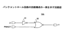
図4は、バンクコントロール回路16Aの回路構成の一例を示す回路図である。
【0036】
図4のバンクコントロール回路16Aは、インバータ31とNOR回路32を含む。プログラム或いはイレーズコマンドが外部から入力された場合には、書き換えコマンド入力を示す信号ZがHIGHであり、パスワード動作信号PWACTがLOWであるので、リード/ライト選択信号Yはライトを指示するHIGHとなる。またパスワードプログラムコマンドが外部から入力された場合には、書き換えを指示する信号ZがHIGHであるが、パスワード動作信号PWACTがHIGHであるので、リード/ライト選択信号Yはリードを指示するLOWとなる。
【0037】
図5は、バンクA選択回路17Aの回路構成の一例を示す回路図である。
【0038】
図5のバンクA選択回路17Aは、インバータ41乃至48、NMOSトランジスタ49乃至51、及びNAND回路52乃至55を含む。インバータ44及び45が、バンク選択状態をラッチするラッチ回路を形成する。ラッチ回路は、ラッチ信号Xに応答して、バンクA21選択時にHIGHとなるバンク選択信号APBKをラッチする。
【0039】
プログラム或いはイレーズコマンドが外部から入力された場合には、リード/ライト選択信号YはHIGHであり、パスワード動作信号PWACTはLOWである。従って、ラッチ回路の出力(バンク選択信号APBKの反転信号)が、NMOSトランジスタ50、NAND回路52、NAND回路53、及びインバータ46を介して、論理反転されて書き換え指示信号ABWSELとして出力される。従って、バンクA21が選択されている場合に、書き換え指示信号ABWSELはHIGHになる。
【0040】
またラッチ回路の出力は、NMOSトランジスタ50、NAND回路52、及びインバータ48を介して、NAND回路54に供給される。NAND回路54の2つの入力は、バンク選択信号APBK及びその論理反転(ラッチ回路出力)であるので、読み出し指示信号ABRSELはバンク選択状態に関わらずLOWとなる。
【0041】
リードコマンドが外部から入力された場合には、リード/ライト選択信号YはLOWであり、パスワード動作信号PWACTもLOWである。従って、書き換え指示信号ABWSELはバンク選択状態に関わらずLOWとなる。またバンク選択信号APBKは、NMOSトランジスタ51、NAND回路52、及びインバータ48を介して、NAND回路54に供給される。NAND回路54の2つの入力は、双方共にバンク選択信号APBKであるので、読み出し指示信号ABRSELはバンク選択時にHIGHとなる。
【0042】
パスワードプログラムコマンドが外部から入力された場合には、リード/ライト選択信号YはLOWであり、パスワード動作信号PWACTがHIGHである。従って、NAND回路52及び55の出力が双方共にHIGHとなり、書き換え指示信号ABWSELはHIGH、読み出し指示信号ABRSELはLOWとなる。
【0043】
図6は、バンク選択回路の回路構成の一例を示す回路図である。バンクB選択回路18、バンクC選択回路19、及びバンクD選択回路20は、図6の回路構成である。
【0044】
図6のバンク選択回路は、インバータ61乃至67、NMOSトランジスタ68乃至70、及びNAND回路71及び72を含む。インバータ62及び63が、バンク選択状態をラッチするラッチ回路を形成する。ラッチ回路は、ラッチ信号Xに応答して、当該バンク選択時にHIGHとなるバンク選択信号qPBK(q=B,C,or D)をラッチする。
【0045】
プログラム或いはイレーズコマンドが外部から入力された場合には、リード/ライト選択信号YはHIGHである。従って、ラッチ回路の出力(バンク選択信号qPBKの反転信号)が、NMOSトランジスタ69、インバータ64、NAND回路71、及びインバータ66を介して、論理反転されて書き換え指示信号qBWSELとして出力される。従って、当該バンクが選択されている場合に、書き換え指示信号qBWSELはHIGHになる。
【0046】
またラッチ回路の出力は、NMOSトランジスタ69、インバータ64、及びインバータ65を介して、NAND回路72に供給される。NAND回路72の2つの入力は、バンク選択信号qPBK及びその論理反転(ラッチ回路出力)であるので、読み出し指示信号qBRSELはバンク選択状態に関わらずLOWとなる。
【0047】
リードコマンドが外部から入力された場合、及びパスワードプログラムコマンドが外部から入力された場合には、リード/ライト選択信号YはLOWである。従って、書き換え指示信号qBWSELはバンク選択状態に関わらずLOWとなる。またバンク選択信号qPBKは、NMOSトランジスタ70、インバータ64、及びインバータ65を介して、NAND回路72に供給される。NAND回路72の2つの入力は、双方共にバンク選択信号qPBKであるので、読み出し指示信号qBRSELは当該バンク選択時にHIGHとなる。
【0048】
図7は、図4乃至図6の回路の動作を示すタイミング図である。図7は、最初にリード状態であり、その後パスワードプログラム状態になる場合を示す。またバンクA選択回路17Aの動作と、バンクB乃至Dを代表してバンクB選択回路18の動作を示す。
【0049】
リード状態においては、書き換えコマンド入力を示す信号Z及びパスワード動作信号PWACTはLOWであり、リード/ライト選択信号Yはリードを指示するLOWである。この時、バンク選択信号APBKがHIGHになりバンクA21を選択すると、バンクA21に対する読み出し指示信号ABRSELがHIGHとなる。またバンク選択信号BPBKがHIGHになりバンクB22を選択すると、バンクB22に対する読み出し指示信号BBRSELがHIGHとなる。
【0050】
その後のパスワードプログラム状態においては、書き換え動作を指示する信号Z及びパスワード動作信号PWACTはHIGHであり、リード/ライト選択信号Yはリードを指示するLOWである。ラッチ信号XがHIGHパルスとして供給されるので、バンクA21の非選択状態を示すLOWのバンク選択信号APBKがラッチされるが、それとは無関係に、パスワード動作信号PWACTのHIGHに応答して、書き換え指示信号ABWSELがHIGHになる。またリード/ライト選択信号Yはリードを指示するLOWのままであるので、ラッチ信号Xに応答してバンクB22の選択状態を示すHIGHのバンク選択信号BPBKがラッチされても、バンクB22に対して書き込み動作が設定されることはない。
【0051】
以上、本発明を実施例に基づいて説明したが、本発明は上記実施例に限定されるものではなく、特許請求の範囲に記載の範囲内で様々な変形が可能である。
【0052】
【発明の効果】
本発明による不揮発性半導体記憶装置においては、パスワードプログラムコマンド入力の場合に、OTP領域が対応するバンクのバンク選択回路はバンク選択状態とは無関係に書き換え指示を出力し、それ以外のバンク選択回路はバンク選択されても書き換え指示でなく読み出し指示を出力する。従って、OTP領域に対応するバンク以外のバンクがバンク選択信号により選択されても、書き換え動作が設定されることがないので、デュアルオペレーションにおいて当該バンクに対して読み出し動作を実行することが出来る。またOTP領域が対応するバンクに対しては、適切にプログラム動作を実行することが出来る。
【0053】
従って、デュアルオペレーションが可能であると共に、アドレス指定無しで適切なパスワードプログラム動作が可能となる。
【図面の簡単な説明】
【図1】デュアルオペレーション動作の不揮発性半導体記憶装置の概略構成を示す構成図である。
【図2】本発明による不揮発性半導体記憶装置の概略構成を示す図である。
【図3】本発明におけるバスワードプログラム動作のタイミング図である。
【図4】バンクコントロール回路の回路構成の一例を示す回路図である。
【図5】バンクA選択回路の回路構成の一例を示す回路図である。
【図6】他のバンク選択回路の回路構成の一例を示す回路図である。
【図7】図4乃至図6の回路の動作を示すタイミング図である。
【符号の説明】
10 不揮発性半導体記憶装置
11 コマンドレジスタ
12、12A コマンドデコーダ
13 制御回路
14 ラッチ信号発生回路
15 バンクデコーダ
16、16A バンクコントロール回路
17、17A バンクA選択回路
18 バンクB選択回路
19 バンクC選択回路
20 バンクD選択回路
21 バンクA
22 バンクB
23 バンクC
24 バンクD
25 OTP領域
30 不揮発性半導体記憶装置[0001]
BACKGROUND OF THE INVENTION
The present invention generally relates to a nonvolatile semiconductor memory device, and more particularly to a nonvolatile semiconductor memory device having a data protection function using a password.
[0002]
[Prior art]
In a nonvolatile semiconductor memory device of dual operation operation, a memory cell array is divided into, for example, four banks, and while a rewrite operation (program operation / erase operation) is performed on a certain bank, A read operation can be performed.
[0003]
FIG. 1 is a configuration diagram showing a schematic configuration of a dual operation non-volatile semiconductor memory device.
[0004]
1 includes a
[0005]
The
[0006]
The latch
[0007]
In response to the signal Z indicating the rewrite command input from the
[0008]
Assume that a read command is input from the outside to the
[0009]
As described above, in the dual operation nonvolatile semiconductor memory device, a read operation is performed on another bank while a rewrite operation (program operation / erase operation) is performed on a certain bank. I can do it.
[0010]
Some recent nonvolatile semiconductor memory devices are provided with a protection function, and the rewriting of stored contents is prohibited at once for each erasing unit called a sector or a block or a plurality of erasing units. I can do it. Information related to storage areas (sectors or blocks) for which rewriting is prohibited is stored in a non-volatile element as a protected state, and the control circuit (state machine) inside the non-volatile semiconductor memory device is protected by referring to this information. The rewriting of the existing area is prohibited.
[0011]
A password mode is provided so that the protected state cannot be freely changed. In the password mode, the nonvolatile element that stores the protected state is locked in a non-rewritable state, and the protected state cannot be changed by default. When the password stored in the non-volatile memory matches the input password from the outside, the lock is released and the protected state can be changed. This unlocking operation is called password unlock.
[0012]
The area of the non-volatile memory that stores the bus word is called an OTP (One Time Protect) area, and is a memory area outside the main storage area. Once the OTP area is protected, it cannot be removed again. In the normal access mode, the OTP area cannot be accessed, and it is necessary to use the OTP mode in order to access the OTP area. When the OTP mode is entered, an arbitrary one sector in the main storage area and the OTP area are logically replaced, and an address for accessing the sector can be input to access the OTP area. Since the password is stored in a part of the OTP area, the OTP mode is always set when the password function is used.
[0013]
[Problems to be solved by the invention]
In the nonvolatile
[0014]
There is no need to inform the user of the location of the area storing the password. Therefore, in the password program operation (password write operation), it is preferable that the password can be written only by inputting the password program command without inputting the address for designating the address. Further, it is preferable that a dual operation in which a read operation is performed on another bank while executing a password program operation is possible.
[0015]
However, when a password program command is input without specifying an address, the selected state of a bank other than the bank A21 may be latched by the bank selection circuit because the address input is don't care. For example, when the bank selection state is latched in the bank
[0016]
In view of the above, an object of the present invention is to provide a nonvolatile semiconductor memory device capable of dual operation and capable of an appropriate password program operation without addressing.
[0017]
[Means for Solving the Problems]
A nonvolatile semiconductor memory device according to the present invention includes a plurality of banks each including an independent memory cell array, a password storage area provided corresponding to one of the plurality of banks, and a bank selection signal by decoding a bank address. A bank decoder that generates the first bank, a first bank selection circuit that outputs a rewrite instruction or read instruction to the one bank, and a rewrite instruction or read instruction to each of the plurality of banks other than the one bank A plurality of second bank selection circuits that output the first command and the first or second bank selection circuit selected by the bank selection signal in the case of a first command input, outputs a rewrite instruction or a read instruction, In the case of command input of 2, the first bank selection circuit outputs a rewrite instruction independently of the bank selection signal; Bank select circuit wherein the second to output a read instruction is selected by the bank selection signal, characterized in that it comprises a command decoder and a bank control circuit for controlling the bank selection circuit.
[0018]
In the nonvolatile semiconductor memory device, in the case of the second command input which is the password program command input, the bank selection circuit of the bank corresponding to the password storage area (OTP area) issues a rewrite instruction regardless of the bank selection state. The other bank selection circuits output a read instruction instead of a rewrite instruction even if a bank is selected. Therefore, even if a bank other than the bank corresponding to the password storage area is selected by the bank selection signal, the rewrite operation is not set, so that the read operation can be executed for the bank in the dual operation. Also, the program operation can be appropriately executed for the bank corresponding to the password storage area.
[0019]
DETAILED DESCRIPTION OF THE INVENTION
Hereinafter, embodiments of the present invention will be described in detail with reference to the accompanying drawings.
[0020]
FIG. 2 is a diagram showing a schematic configuration of a nonvolatile semiconductor memory device according to the present invention.
[0021]
2 includes a
[0022]
The
[0023]
The
[0024]
The latch
[0025]
In the case of a rewrite operation, when the
[0026]
When the input bank address indicates, for example, the bank B22, the bank
[0027]
In the case of the password program operation, the
[0028]
In response to the signal PWACT from the
[0029]
In the bank
[0030]
Assume that a read command is input from the outside to the
[0031]
As described above, in the nonvolatile semiconductor memory device of the dual operation operation of the present invention, the password program operation is executed by inputting the password program command without addressing, and the password program operation is performed for a certain bank. In the meantime, a read operation can be executed on another bank.
[0032]
FIG. 3 is a timing diagram of the bus word program operation in the present invention.
[0033]
As shown in FIG. 3, a password program command (Add: 55H & I / O: 38H) is input in synchronization with the chip enable signal / CE or the write enable signal / WE. At the next timing, password data PWD to be written as input / output data I / O is input, and address data Add is don't care. In response to the chip enable signal / CE or the write enable signal / WE, the latch signal X is generated by the latch
[0034]
Since the address input is don't care, it is unclear which bank selection state for selecting which bank is latched by the bank selection circuit. In this state, when the read / write selection signal Y becomes HIGH (write instruction) at the timing indicated by T0 in FIG. 3, not the bank A21 with the OTP area 25 but other banks are set to the write operation. There is a risk of being done. In the present invention, the read / write selection signal Y is set to LOW (read instruction) by the password operation signal PWACT to set all banks to the read state. However, the bank A21 is forcibly set to the write state by the password operation signal PWACT.
[0035]
FIG. 4 is a circuit diagram showing an example of the circuit configuration of the
[0036]
The
[0037]
FIG. 5 is a circuit diagram showing an example of the circuit configuration of the bank
[0038]
The bank
[0039]
When a program or erase command is input from the outside, the read / write selection signal Y is HIGH, and the password operation signal PWACT is LOW. Therefore, the output of the latch circuit (inverted signal of the bank selection signal APBK) is logically inverted through the
[0040]
The output of the latch circuit is supplied to the NAND circuit 54 via the
[0041]
When a read command is input from the outside, the read / write selection signal Y is LOW, and the password operation signal PWACT is also LOW. Therefore, the rewrite instruction signal ABWSEL is LOW regardless of the bank selection state. The bank selection signal APBK is supplied to the NAND circuit 54 via the
[0042]
When the password program command is input from the outside, the read / write selection signal Y is LOW and the password operation signal PWACT is HIGH. Accordingly, the outputs of the
[0043]
FIG. 6 is a circuit diagram showing an example of the circuit configuration of the bank selection circuit. The bank
[0044]
The bank selection circuit in FIG. 6 includes inverters 61 to 67, NMOS transistors 68 to 70, and
[0045]
When a program or erase command is input from the outside, the read / write selection signal Y is HIGH. Accordingly, the output of the latch circuit (inverted signal of the bank selection signal qPBK) is logically inverted through the
[0046]
The output of the latch circuit is supplied to the
[0047]
When a read command is input from the outside and when a password program command is input from the outside, the read / write selection signal Y is LOW. Therefore, the rewrite instruction signal qBWSEL is LOW regardless of the bank selection state. The bank selection signal qPBK is supplied to the
[0048]
FIG. 7 is a timing diagram showing the operation of the circuits of FIGS. FIG. 7 shows a case where a read state is first set and then a password program state is set. The operation of the bank
[0049]
In the read state, the signal Z indicating the input of the rewrite command and the password operation signal PWACT are LOW, and the read / write selection signal Y is LOW for instructing reading. At this time, when the bank selection signal APBK becomes HIGH and the bank A21 is selected, the read instruction signal ABRSEL for the bank A21 becomes HIGH. When the bank selection signal BPBK becomes HIGH and the bank B22 is selected, the read instruction signal BBRSEL for the bank B22 becomes HIGH.
[0050]
In the subsequent password program state, the signal Z for instructing the rewrite operation and the password operation signal PWACT are HIGH, and the read / write selection signal Y is LOW for instructing reading. Since the latch signal X is supplied as a HIGH pulse, the LOW bank selection signal APBK indicating the non-selected state of the bank A21 is latched. Regardless of this, a rewrite instruction is issued in response to the HIGH of the password operation signal PWACT. Signal ABWSEL goes HIGH. Since the read / write selection signal Y remains LOW for instructing reading, even if the HIGH bank selection signal BPBK indicating the selection state of the bank B22 in response to the latch signal X is latched, No write operation is set.
[0051]
As mentioned above, although this invention was demonstrated based on the Example, this invention is not limited to the said Example, A various deformation | transformation is possible within the range as described in a claim.
[0052]
【The invention's effect】
In the nonvolatile semiconductor memory device according to the present invention, when a password program command is input, the bank selection circuit of the bank to which the OTP region corresponds outputs a rewrite instruction regardless of the bank selection state, and the other bank selection circuits Even if a bank is selected, a read instruction is output instead of a rewrite instruction. Therefore, even if a bank other than the bank corresponding to the OTP region is selected by the bank selection signal, the rewrite operation is not set, so that the read operation can be executed for the bank in the dual operation. Further, the program operation can be appropriately executed for the bank corresponding to the OTP area.
[0053]
Accordingly, dual operation is possible, and an appropriate password program operation can be performed without specifying an address.
[Brief description of the drawings]
FIG. 1 is a configuration diagram showing a schematic configuration of a nonvolatile semiconductor memory device of dual operation operation.
FIG. 2 is a diagram showing a schematic configuration of a nonvolatile semiconductor memory device according to the present invention.
FIG. 3 is a timing diagram of a bus word program operation in the present invention.
FIG. 4 is a circuit diagram showing an example of a circuit configuration of a bank control circuit.
FIG. 5 is a circuit diagram showing an example of a circuit configuration of a bank A selection circuit.
FIG. 6 is a circuit diagram showing an example of a circuit configuration of another bank selection circuit.
FIG. 7 is a timing chart showing the operation of the circuits of FIGS. 4 to 6;
[Explanation of symbols]
10 Nonvolatile semiconductor memory device
11 Command register
12, 12A Command decoder
13 Control circuit
14 Latch signal generation circuit
15 bank decoder
16, 16A Bank control circuit
17, 17A Bank A selection circuit
18 Bank B selection circuit
19 Bank C selection circuit
20 Bank D selection circuit
21 Bank A
22 Bank B
23 Bank C
24 Bank D
25 OTP region
30 Nonvolatile semiconductor memory device
Claims (10)
該複数のバンクうち1つのバンクに対応して設けられるパスワード格納領域と、
バンクアドレスをデコードしてバンク選択信号を生成するバンクデコーダと、
該1つのバンクに対して書き換え指示又は読み出し指示を出力する第1のバンク選択回路と、
該1つのバンク以外の該複数のバンクのそれぞれに対して書き換え指示又は読み出し指示を出力する複数の第2のバンク選択回路と、
第1のコマンド入力の場合に該バンク選択信号により選択される該第1或いは第2のバンク選択回路が書き換え指示又は読み出し指示を出力し、第2のコマンド入力の場合に該第1のバンク選択回路が該バンク選択信号とは独立に書き換え指示を出力し且つ該第2のバンク選択回路が該バンク選択信号で選択されると読み出し指示を出力するように、該第1及び第2のバンク選択回路を制御するコマンドデコーダ&バンクコントロール回路
を含むことを特徴とする不揮発性半導体記憶装置。A plurality of banks each including an independent memory cell array;
A password storage area provided corresponding to one of the plurality of banks;
A bank decoder for decoding a bank address and generating a bank selection signal;
A first bank selection circuit that outputs a rewrite instruction or a read instruction to the one bank;
A plurality of second bank selection circuits for outputting a rewrite instruction or a read instruction to each of the plurality of banks other than the one bank;
In the case of a first command input, the first or second bank selection circuit selected by the bank selection signal outputs a rewrite instruction or a read instruction, and in the case of a second command input, the first bank selection The first and second bank selections so that a circuit outputs a rewrite instruction independent of the bank selection signal and a second bank selection circuit outputs a read instruction when selected by the bank selection signal A non-volatile semiconductor memory device comprising a command decoder & bank control circuit for controlling a circuit.
バンクアドレスをデコードしてバンク選択信号を生成するバンクデコーダと、
該複数のバンクのそれぞれに対して設けられアドレス指定を伴うコマンド入力の場合に該バンク選択信号により選択されると書き換え指示又は読み出し指示を対応するバンクに出力する複数のバンク選択回路
を含み、該複数のバンク選択回路の1つはアドレス指定を伴わないコマンド入力の場合に該バンク選択信号とは独立に該書き換え指示を出力することを特徴とする不揮発性半導体記憶装置。A plurality of banks each including an independent memory cell array;
A bank decoder for decoding a bank address and generating a bank selection signal;
A plurality of bank selection circuits which are provided for each of the plurality of banks and output a rewrite instruction or a read instruction to a corresponding bank when selected by the bank selection signal in the case of command input with address designation; A nonvolatile semiconductor memory device, wherein one of a plurality of bank selection circuits outputs the rewrite instruction independently of the bank selection signal when a command is input without address designation.
Priority Applications (2)
| Application Number | Priority Date | Filing Date | Title |
|---|---|---|---|
| JP2001320909A JP3961806B2 (en) | 2001-10-18 | 2001-10-18 | Nonvolatile semiconductor memory device |
| US10/263,646 US6711055B2 (en) | 2001-10-18 | 2002-10-04 | Nonvolatile semiconductor memory device of dual-operation type with data protection function |
Applications Claiming Priority (1)
| Application Number | Priority Date | Filing Date | Title |
|---|---|---|---|
| JP2001320909A JP3961806B2 (en) | 2001-10-18 | 2001-10-18 | Nonvolatile semiconductor memory device |
Publications (2)
| Publication Number | Publication Date |
|---|---|
| JP2003123489A JP2003123489A (en) | 2003-04-25 |
| JP3961806B2 true JP3961806B2 (en) | 2007-08-22 |
Family
ID=19138221
Family Applications (1)
| Application Number | Title | Priority Date | Filing Date |
|---|---|---|---|
| JP2001320909A Expired - Fee Related JP3961806B2 (en) | 2001-10-18 | 2001-10-18 | Nonvolatile semiconductor memory device |
Country Status (2)
| Country | Link |
|---|---|
| US (1) | US6711055B2 (en) |
| JP (1) | JP3961806B2 (en) |
Families Citing this family (6)
| Publication number | Priority date | Publication date | Assignee | Title |
|---|---|---|---|---|
| KR100558486B1 (en) * | 2003-07-14 | 2006-03-07 | 삼성전자주식회사 | Nonvolatile semiconductor memory device and one time programming control method thereof |
| JP2005317127A (en) * | 2004-04-28 | 2005-11-10 | Matsushita Electric Ind Co Ltd | Nonvolatile semiconductor storage device |
| US9256525B2 (en) | 2011-12-02 | 2016-02-09 | Kabushiki Kaisha Toshiba | Semiconductor memory device including a flag for selectively controlling erasing and writing of confidential information area |
| JP5885638B2 (en) * | 2011-12-02 | 2016-03-15 | 株式会社東芝 | Semiconductor memory device |
| US9620216B2 (en) | 2015-02-17 | 2017-04-11 | Silicon Storage Technology, Inc. | Flash memory device configurable to provide read only memory functionality |
| US10141042B1 (en) * | 2017-05-23 | 2018-11-27 | Micron Technology, Inc. | Method and apparatus for precharge and refresh control |
Family Cites Families (5)
| Publication number | Priority date | Publication date | Assignee | Title |
|---|---|---|---|---|
| JPH0812646B2 (en) * | 1989-03-03 | 1996-02-07 | 三菱電機株式会社 | Semiconductor integrated circuit |
| US6009495A (en) * | 1989-12-29 | 1999-12-28 | Packard Bell Nec | Protected address range in an electrically erasable programmable read only memory |
| TW231343B (en) * | 1992-03-17 | 1994-10-01 | Hitachi Seisakusyo Kk | |
| US6031757A (en) * | 1996-11-22 | 2000-02-29 | Macronix International Co., Ltd. | Write protected, non-volatile memory device with user programmable sector lock capability |
| JPH11110293A (en) * | 1997-09-29 | 1999-04-23 | Mitsubishi Electric Corp | Nonvolatile memory control circuit |
-
2001
- 2001-10-18 JP JP2001320909A patent/JP3961806B2/en not_active Expired - Fee Related
-
2002
- 2002-10-04 US US10/263,646 patent/US6711055B2/en not_active Expired - Lifetime
Also Published As
| Publication number | Publication date |
|---|---|
| JP2003123489A (en) | 2003-04-25 |
| US20030076730A1 (en) | 2003-04-24 |
| US6711055B2 (en) | 2004-03-23 |
Similar Documents
| Publication | Publication Date | Title |
|---|---|---|
| US6556504B2 (en) | Nonvolatile semiconductor memory device and data input/output control method thereof | |
| JP3884839B2 (en) | Semiconductor memory device | |
| US5749088A (en) | Memory card with erasure blocks and circuitry for selectively protecting the blocks from memory operations | |
| US20050071592A1 (en) | Selectable block protection for non-volatile memory | |
| US7203791B2 (en) | Flash memory device with partial copy-back mode | |
| JP2002202911A (en) | Nonvolatile memory | |
| US5765184A (en) | Method and apparatus for programming an array controller in a flash memory device | |
| JPH11110293A (en) | Nonvolatile memory control circuit | |
| JP2001084780A (en) | Nonvolatile semiconductor memory | |
| JP2002329396A (en) | Flash memory whose bank constitution can be modified | |
| JP4678083B2 (en) | Memory device and memory access restriction method | |
| JP3961806B2 (en) | Nonvolatile semiconductor memory device | |
| JPH11242632A (en) | Memory device | |
| JPWO2006046282A1 (en) | Nonvolatile storage device | |
| US7099226B2 (en) | Functional register decoding system for multiple plane operation | |
| JP2002222084A (en) | Semiconductor storage device, sector address conversion circuit, address conversion method, and method for using semiconductor storage device | |
| JP4138291B2 (en) | Nonvolatile semiconductor memory device and control method thereof | |
| JPH07153284A (en) | Non-volatile semiconductor memory and its control method | |
| JP2003051195A (en) | Semiconductor memory device | |
| JP3872922B2 (en) | Semiconductor memory device and memory embedded logic LSI | |
| JP2000181802A (en) | Semiconductor storage device | |
| JP2000066949A (en) | Data recording/reproducing device and memory accessing method for the data recording/reproducing device | |
| JP2002197890A (en) | Nonvolatile semiconductor memory | |
| JP3625812B2 (en) | Non-volatile memory | |
| JP3821911B2 (en) | Memory initialization control method |
Legal Events
| Date | Code | Title | Description |
|---|---|---|---|
| A621 | Written request for application examination |
Free format text: JAPANESE INTERMEDIATE CODE: A621 Effective date: 20040915 |
|
| TRDD | Decision of grant or rejection written | ||
| A01 | Written decision to grant a patent or to grant a registration (utility model) |
Free format text: JAPANESE INTERMEDIATE CODE: A01 Effective date: 20070424 |
|
| A61 | First payment of annual fees (during grant procedure) |
Free format text: JAPANESE INTERMEDIATE CODE: A61 Effective date: 20070517 |
|
| R150 | Certificate of patent or registration of utility model |
Free format text: JAPANESE INTERMEDIATE CODE: R150 |
|
| S111 | Request for change of ownership or part of ownership |
Free format text: JAPANESE INTERMEDIATE CODE: R313111 |
|
| FPAY | Renewal fee payment (event date is renewal date of database) |
Free format text: PAYMENT UNTIL: 20100525 Year of fee payment: 3 |
|
| R350 | Written notification of registration of transfer |
Free format text: JAPANESE INTERMEDIATE CODE: R350 |
|
| FPAY | Renewal fee payment (event date is renewal date of database) |
Free format text: PAYMENT UNTIL: 20100525 Year of fee payment: 3 |
|
| FPAY | Renewal fee payment (event date is renewal date of database) |
Free format text: PAYMENT UNTIL: 20110525 Year of fee payment: 4 |
|
| FPAY | Renewal fee payment (event date is renewal date of database) |
Free format text: PAYMENT UNTIL: 20110525 Year of fee payment: 4 |
|
| S531 | Written request for registration of change of domicile |
Free format text: JAPANESE INTERMEDIATE CODE: R313531 |
|
| S533 | Written request for registration of change of name |
Free format text: JAPANESE INTERMEDIATE CODE: R313533 |
|
| FPAY | Renewal fee payment (event date is renewal date of database) |
Free format text: PAYMENT UNTIL: 20110525 Year of fee payment: 4 |
|
| R350 | Written notification of registration of transfer |
Free format text: JAPANESE INTERMEDIATE CODE: R350 |
|
| FPAY | Renewal fee payment (event date is renewal date of database) |
Free format text: PAYMENT UNTIL: 20120525 Year of fee payment: 5 |
|
| FPAY | Renewal fee payment (event date is renewal date of database) |
Free format text: PAYMENT UNTIL: 20120525 Year of fee payment: 5 |
|
| FPAY | Renewal fee payment (event date is renewal date of database) |
Free format text: PAYMENT UNTIL: 20130525 Year of fee payment: 6 |
|
| FPAY | Renewal fee payment (event date is renewal date of database) |
Free format text: PAYMENT UNTIL: 20140525 Year of fee payment: 7 |
|
| S111 | Request for change of ownership or part of ownership |
Free format text: JAPANESE INTERMEDIATE CODE: R313111 |
|
| R350 | Written notification of registration of transfer |
Free format text: JAPANESE INTERMEDIATE CODE: R350 |
|
| LAPS | Cancellation because of no payment of annual fees |