JP3961663B2 - Digital mobile radio - Google Patents
Digital mobile radio Download PDFInfo
- Publication number
- JP3961663B2 JP3961663B2 JP11440298A JP11440298A JP3961663B2 JP 3961663 B2 JP3961663 B2 JP 3961663B2 JP 11440298 A JP11440298 A JP 11440298A JP 11440298 A JP11440298 A JP 11440298A JP 3961663 B2 JP3961663 B2 JP 3961663B2
- Authority
- JP
- Japan
- Prior art keywords
- transmission
- reception
- capacitor
- mobile radio
- circuit
- Prior art date
- Legal status (The legal status is an assumption and is not a legal conclusion. Google has not performed a legal analysis and makes no representation as to the accuracy of the status listed.)
- Expired - Fee Related
Links
Images

Landscapes
- Transceivers (AREA)
Description
【0001】
【発明の属する技術分野】
本発明はディジタル移動無線機に関し、特に、バッテリセービングのため、そのシンセサイザの送受信周波数帯域切替部の改良に関すものである。
【0002】
【従来の技術】
携帯電話等の移動体通信システムにおいては、ディジタル無線伝送技術,高能率音声符号化技術等の急激な進歩によりIC化が進み、小形化と周波数の有効利用のためにディジタル変復調方式の移動無線機が急速に実用化されてきた。
【0003】
TDMA(時分割多元接続)は、例えば、900MHz帯の移動無線機におけるディジタル方式の代表的な回線制御のアクセス技術であり、1TDMAフレームは複数のチャネル(スロット)で構成され、移動機は自局に割当てられた送信スロットと受信スロットでバースト的に送信後受信し、更に空時間があって、周囲の基地局からの電波の強さをモニタすることができる。
【0004】
公衆用,業務用など携帯無線の各運用システムには基地送信周波数帯域と移動送信周波数帯域が割り当てられている。
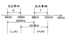
図2は周波数帯域の割当例図である。この例では、移動受信帯域(R)は移動送信帯域(T)より低い周波数に割り当てられており、移動機の送信スロットの周波数と受信スロットの周波数は、45MHzの間隔で運用される。
【0005】
このようなディジタル移動無線機に対しては、フェージングに強く、占有帯域が狭く、干渉に強いことは勿論、小形化と電池持続時間をできるだけ長くするため、消費電力が少ないことが求められている。
【0006】
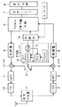
図3は本発明を適用しようとするディジタル移動無線機のブロック図である。図において、1は送受分波器、2は低雑音増幅器(LNA)、3はバンドパスフィルタ(BPF)、4はミキサ、5は復調器、6はTDMA多重分離回路、7は音声コーデック、8は音声回路、9は変調器、10はミキサ、11はBPF、12は電力増幅器(PA)、13は周波数シンセサイザ、13−1は電圧制御発振器(VCO)、14は制御部、15は切替器である。
【0007】
VCO13−1から出力される周波数シンセサイザ13の出力cは、切替器15によって受信用ミキサ4と送信用ミキサ10に切替え供給される。この場合、VCO13−1は、制御部14からの送受帯域切替信号bによって、受信時は受信帯域Rの自局のチャネル周波数信号cを出力して受信ミキサ4に供給し、送信時は送信帯域Tの自局チャネル周波数信号cを出力して送信ミキサ10に供給するように構成されている。信号aは自局のチャネル周波数に合わせるためのVCO13−1の制御電圧である。
【0008】
図4は従来のVCOの詳細回路図である。図において、21は共振回路であり、誘電体共振器Zとバラクタダイオード(可変容量ダイオード)CR0 が並列接続され、制御電圧aによって共振周波数を5.4MHz〜7.9±0.8MHz/Vの範囲で変化させることができる。22は発振回路であり、共振回路21と接続されて900MHz帯の発振信号をバッファ段を介して出力する。24は周波数帯域切替部であり、共振回路21の誘電体共振器Zに並列に接続して発振周波数帯域を変える(下げる)ための付加コンデンサC1 と、その接地をオン/オフ(接/断)するスイッチ回路23とからなり、制御部14からの送受帯域切替信号bにより、ピンダイオードCR1 ,CR2 に与えるバイアス電流をオン/オフしてコンデンサC1 をオン/オフする。
【0009】
【発明が解決しようとする課題】
しかしながら、上記従来の回路では、スイッチ回路23をオンにしてコンデンサC1 を接続したとき、VCOの出力は周波数の低い受信帯域(R)となり、無線機の送信時間より長い受信待ち受け時間に、スイッチ回路23のピンダイオードCR2 ,CR3 に流れる電力が消費するという問題がある。
この場合、スイッチ回路23がオンの状態で待ち受け時間のとき、スイッチ回路23に約5mAの電流が流れ、VCO全体では18mAの電流が流れる。
【0010】
本発明の目的は、上記待ち受け時に消費するスイッチ回路23の電力を0にして、その分、無線機の消費電力を低減するように構成した移動無線機を提供することにある。
【0011】
【課題を解決するための手段】
本発明の移動無線機は、受信周波数帯域が送信周波数帯域より低く割当てられたTDMA方式のディジタル移動無線システムの送受信機であって、
局部発振手段として設けられた電圧制御発振器の共振回路に並列接続された付加リアクタンスを送受帯域切替信号によりオン/オフすることによって送信スロットと受信スロットの局発信号を送信側ミキサと受信側ミキサに対して切替え出力する周波数シンセサイザが備えられたディジタル移動無線機において、
前記付加リアクタンスは、前記共振回路に並列接続された第1のコンデンサとコイルとの直列回路と、該コイルと並列に設けられ前記送受帯域切替信号によりオン/オフされる第2のコンデンサとからなり、
前記第1のコンデンサ,前記コイル,前記第2のコンデンサの値は、該第2のコンデンサがオフのときの前記付加リアクタンスのインピーダンスが、オンのときのインピーダンスより大きく、かつ、オフの時とオンの時の前記電圧制御発振器の出力周波数の差が所定の値になるように設定され、オフのとき受信周波数帯域となるように構成したことを特徴とするものである。
【0012】
【発明の実施の形態】
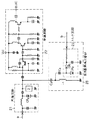
図1は本発明の要部をなすVCOの詳細回路図である。図4の従来回路との違いは、周波数帯域切替部25の付加リアクタンスを、コンデンサC2 とコイルL1 の直列回路と、コイルL1 と並列にコンデンサC3 をスイッチ回路23を介して設けたことにある。
【0013】
このように周波数帯域切替部25の回路を構成し、送受帯域切替信号bの極性を逆にすると、スイッチ回路23をオンにしたときVCOの発振周波数を周波数の高い送信帯域にすることができる。そのために、2つのコンデンサC2 ,C3 とコイルL1 の値は、次のように設定する。
【0014】
スイッチ回路23がオフのときのインピーダンス、すなわち、コンデンサC2 とコイルL1 の直列回路のインピーダンスをXOFF とし、スイッチ回路23がオンのときのコイルL1 とコンデンサC3 の並列インピーダンスとコンデンサC2 とのインピーダンスをXONとしたとき、XOFF >XONの関係で、かつ、送信/受信周波数の差が所定の値、例えば45MHzになるように設定する。次の表1は具体例である。
【0015】
【表1】
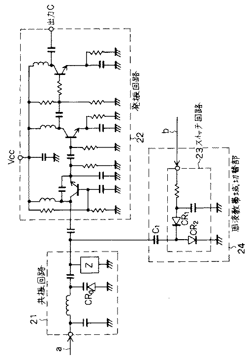
図1の周波数帯域切替部25のコンデンサC2 の値をできるだけ小さくすることにより、コイルL1 による共振回路のQの低下を最小限に抑えることができる。これは、コイルL1 による損失を軽減する手段の一つである。
【0017】
【発明の効果】
以上詳細に説明したように、本発明を実施することにより、無線機の待ち受け時間には、スイッチ回路23の電流が流れず、待ち受け時間におけるスイッチ回路23の電力消費を0にすることができる。
【図面の簡単な説明】
【図1】本発明の要部であるVCOの実施例を示す回路図である。
【図2】送受信周波数帯域の配列例を示す説明図である。
【図3】本発明を適用する無線受信機のブロック図である。
【図4】従来のVCOの回路例図である。
【符号の説明】
1 送受分波器
2 LNA
3,11 BPF
4,10 ミキサ
5 復調器
6 TDMA多重分離回路
7 音声コーデック
8 音声回路
9 変調器
12 PA
13 周波数シンセサイザ
13−1 VCO
14 制御部
15 切替器
21 共振回路
22 発振回路
23 スイッチ回路
24,25 周波数帯域切替部[0001]
BACKGROUND OF THE INVENTION
The present invention relates to a digital mobile radio, and more particularly to improvement of a transmission / reception frequency band switching unit of a synthesizer for battery saving.
[0002]
[Prior art]
In mobile communication systems such as cellular phones, ICs have advanced due to rapid advances in digital wireless transmission technology, high-efficiency speech coding technology, etc., and digital modulation / demodulation mobile radios have been developed for miniaturization and effective use of frequencies. Has been rapidly put into practical use.
[0003]
TDMA (Time Division Multiple Access) is, for example, a typical digital channel control access technology in a 900 MHz band mobile radio, and one TDMA frame is composed of a plurality of channels (slots). In the transmission slot and the reception slot assigned to, the signal is received after burst transmission, and there is further free time, so that the strength of radio waves from surrounding base stations can be monitored.
[0004]
A base transmission frequency band and a mobile transmission frequency band are assigned to each mobile wireless operation system such as public use and business use.
FIG. 2 is an example of frequency band allocation. In this example, the mobile reception band (R) is assigned to a frequency lower than the mobile transmission band (T), and the frequency of the transmission slot of the mobile station and the frequency of the reception slot are operated at an interval of 45 MHz.
[0005]
Such digital mobile radios are required to have low power consumption in order to reduce size and increase battery duration as much as possible, as well as being resistant to fading, having a narrow occupation band, and being resistant to interference. .
[0006]
FIG. 3 is a block diagram of a digital mobile radio to which the present invention is applied. In the figure, 1 is a transmitter / receiver demultiplexer, 2 is a low noise amplifier (LNA), 3 is a band pass filter (BPF), 4 is a mixer, 5 is a demodulator, 6 is a TDMA demultiplexing circuit, 7 is a speech codec, 8 Is an audio circuit, 9 is a modulator, 10 is a mixer, 11 is a BPF, 12 is a power amplifier (PA), 13 is a frequency synthesizer, 13-1 is a voltage controlled oscillator (VCO), 14 is a control unit, and 15 is a switcher. It is.
[0007]
The output c of the frequency synthesizer 13 output from the VCO 13-1 is switched and supplied to the reception mixer 4 and the transmission mixer 10 by the
[0008]
FIG. 4 is a detailed circuit diagram of a conventional VCO. In the figure, 21 is a resonance circuit, in which a dielectric resonator Z and a varactor diode (variable capacitance diode) CR 0 are connected in parallel, and the resonance frequency is 5.4 MHz to 7.9 ± 0.8 MHz / V by the control voltage a. It can be changed within the range. An
[0009]
[Problems to be solved by the invention]
However, in the above conventional circuit, when the switch circuit 23 is turned on and the capacitor C 1 is connected, the output of the VCO becomes a reception band (R) having a low frequency, and the switch waits for a reception standby time longer than the transmission time of the radio. There is a problem that power flowing through the pin diodes CR 2 and CR 3 of the circuit 23 is consumed.
In this case, when the switch circuit 23 is on and the standby time is reached, a current of about 5 mA flows through the switch circuit 23, and a current of 18 mA flows through the entire VCO.
[0010]
An object of the present invention is to provide a mobile radio device configured to reduce the power consumption of the radio device by setting the power of the switch circuit 23 consumed at the time of standby to zero.
[0011]
[Means for Solving the Problems]
The mobile radio of the present invention is a transceiver of a TDMA digital mobile radio system in which a reception frequency band is allocated lower than a transmission frequency band,
By turning on / off the additional reactance connected in parallel to the resonant circuit of the voltage controlled oscillator provided as the local oscillation means by the transmission / reception band switching signal, the local oscillation signals of the transmission slot and the reception slot are transmitted to the transmission side mixer and the reception side mixer. In a digital mobile radio equipped with a frequency synthesizer for switching output to
The additional reactance includes a series circuit of a first capacitor and a coil connected in parallel to the resonance circuit, and a second capacitor provided in parallel with the coil and turned on / off by the transmission / reception band switching signal. ,
The values of the first capacitor, the coil, and the second capacitor are such that the impedance of the additional reactance when the second capacitor is off is larger than the impedance when it is on, and when it is off and on The difference between the output frequencies of the voltage controlled oscillator at the time is set to be a predetermined value, and when it is off, the reception frequency band is set.
[0012]
DETAILED DESCRIPTION OF THE INVENTION
FIG. 1 is a detailed circuit diagram of a VCO which forms a main part of the present invention. The difference from the conventional circuit of FIG. 4, an additional reactance frequency
[0013]
If the circuit of the frequency
[0014]
The impedance when the switch circuit 23 is off, that is, the impedance of the series circuit of the capacitor C 2 and the coil L 1 is X OFF, and the parallel impedance of the coil L 1 and the capacitor C 3 when the switch circuit 23 is on and the capacitor C when the impedance between 2 and X oN, in relation to X OFF> X oN, and the difference of the transmission / reception frequency is set to be a predetermined value, for example 45 MHz. The following Table 1 is a specific example.
[0015]
[Table 1]
By reducing the value of the capacitor C 2 of the frequency
[0017]
【The invention's effect】
As described in detail above, by implementing the present invention, the current of the switch circuit 23 does not flow during the standby time of the radio, and the power consumption of the switch circuit 23 during the standby time can be reduced to zero.
[Brief description of the drawings]
FIG. 1 is a circuit diagram showing an embodiment of a VCO that is a main part of the present invention.
FIG. 2 is an explanatory diagram showing an exemplary arrangement of transmission / reception frequency bands;
FIG. 3 is a block diagram of a wireless receiver to which the present invention is applied.
FIG. 4 is a circuit diagram of a conventional VCO.
[Explanation of symbols]
1 Transmitter /
3,11 BPF
4, 10
13 Frequency synthesizer 13-1 VCO
14
Claims (1)
局部発振手段として設けられた電圧制御発振器の共振回路に並列接続された付加リアクタンスを送受帯域切替信号によりオン/オフすることによって送信スロットと受信スロットの局発信号を送信側ミキサと受信側ミキサに対して切替え出力する周波数シンセサイザが備えられたディジタル移動無線機において、
前記付加リアクタンスは、前記共振回路に並列接続された第1のコンデンサとコイルとの直列回路と、該コイルと並列に設けられ前記送受帯域切替信号によりオン/オフされる第2のコンデンサとからなり、
前記第1のコンデンサ,前記コイル,前記第2のコンデンサの値は、該第2のコンデンサがオフのときの前記付加リアクタンスのインピーダンスが、オンのときのインピーダンスより大きく、かつ、オフの時とオンの時の前記電圧制御発振器の出力周波数の差が所定の値になるように設定され、オフのとき受信周波数帯域となるように構成したことを特徴とするディジタル移動無線機。A transmitter / receiver of a TDMA type digital mobile radio system in which a reception frequency band is allocated lower than a transmission frequency band,
By turning on / off the additional reactance connected in parallel to the resonant circuit of the voltage controlled oscillator provided as the local oscillation means by the transmission / reception band switching signal, the local oscillation signals of the transmission slot and the reception slot are transmitted to the transmission side mixer and the reception side mixer. In a digital mobile radio equipped with a frequency synthesizer for switching output to
The additional reactance includes a series circuit of a first capacitor and a coil connected in parallel to the resonance circuit, and a second capacitor provided in parallel with the coil and turned on / off by the transmission / reception band switching signal. ,
The values of the first capacitor, the coil, and the second capacitor are such that the impedance of the additional reactance when the second capacitor is off is larger than the impedance when it is on, and when it is off and on A digital mobile radio having a configuration in which a difference in output frequency of the voltage controlled oscillator at a time is set to a predetermined value and a reception frequency band is set when the voltage control oscillator is turned off.
Priority Applications (1)
| Application Number | Priority Date | Filing Date | Title |
|---|---|---|---|
| JP11440298A JP3961663B2 (en) | 1998-04-10 | 1998-04-10 | Digital mobile radio |
Applications Claiming Priority (1)
| Application Number | Priority Date | Filing Date | Title |
|---|---|---|---|
| JP11440298A JP3961663B2 (en) | 1998-04-10 | 1998-04-10 | Digital mobile radio |
Publications (2)
| Publication Number | Publication Date |
|---|---|
| JPH11298363A JPH11298363A (en) | 1999-10-29 |
| JP3961663B2 true JP3961663B2 (en) | 2007-08-22 |
Family
ID=14636794
Family Applications (1)
| Application Number | Title | Priority Date | Filing Date |
|---|---|---|---|
| JP11440298A Expired - Fee Related JP3961663B2 (en) | 1998-04-10 | 1998-04-10 | Digital mobile radio |
Country Status (1)
| Country | Link |
|---|---|
| JP (1) | JP3961663B2 (en) |
-
1998
- 1998-04-10 JP JP11440298A patent/JP3961663B2/en not_active Expired - Fee Related
Also Published As
| Publication number | Publication date |
|---|---|
| JPH11298363A (en) | 1999-10-29 |
Similar Documents
| Publication | Publication Date | Title |
|---|---|---|
| US6195563B1 (en) | Radio receiver and radio transmitter | |
| US8036619B2 (en) | Oscillator having controllable bias modes and power consumption | |
| TW408526B (en) | RF architecture for cellular dual-band telephone | |
| US6708044B1 (en) | Apparatus and method for automated band selection via synthesizer bit insertion | |
| KR100877253B1 (en) | Method and apparatus for multiple band voltage controlled oscillator with noise immunity | |
| JP2705538B2 (en) | Shared receiver for CDMA mode and FM mode | |
| JP2001503592A (en) | Frequency synthesizer circuit for mobile station | |
| JP2855496B2 (en) | Filter switching circuit | |
| US5956326A (en) | System and method for frequency division duplex/time division duplex radio frequency communication | |
| US6069925A (en) | Dual band, dual mode transceiver with adaptive second if switching device | |
| JP4344106B2 (en) | WIRELESS SYSTEM, ANTENNA CONFIGURATION, AND POLARIZATION MODULATOR FOR GENERATING TRANSMISSION SIGNALS WITH POLARIZATION POLARIZATION | |
| KR100631272B1 (en) | Multi-mode mobile communication terminal | |
| CN1154248C (en) | Transceiver and telecommunication system having transceiver | |
| JP3961663B2 (en) | Digital mobile radio | |
| US20020068530A1 (en) | Device and process for coupling multi-band transmitters and receivers and communication system employing same | |
| US6829469B1 (en) | Method and a device for producing a signal | |
| US5493714A (en) | Apparatus and method for automatically controlling a reference frequency in a dual mode receiver | |
| US7466968B2 (en) | Method and apparatus for providing a local oscillator signal | |
| JP2889753B2 (en) | Dual band wireless communication device | |
| US6175724B1 (en) | Band switchable injection oscillator and communication device using same | |
| CN1998149A (en) | Provision of local oscillator signals | |
| JP3281715B2 (en) | Wireless communication device | |
| JPH0474028A (en) | cordless telephone device | |
| JPH05503409A (en) | active filter circuit | |
| JPH1093476A (en) | Transceiver for wireless communication |
Legal Events
| Date | Code | Title | Description |
|---|---|---|---|
| A621 | Written request for application examination |
Free format text: JAPANESE INTERMEDIATE CODE: A621 Effective date: 20050215 |
|
| A977 | Report on retrieval |
Free format text: JAPANESE INTERMEDIATE CODE: A971007 Effective date: 20070417 |
|
| TRDD | Decision of grant or rejection written | ||
| A01 | Written decision to grant a patent or to grant a registration (utility model) |
Free format text: JAPANESE INTERMEDIATE CODE: A01 Effective date: 20070508 |
|
| A61 | First payment of annual fees (during grant procedure) |
Free format text: JAPANESE INTERMEDIATE CODE: A61 Effective date: 20070517 |
|
| R150 | Certificate of patent or registration of utility model |
Free format text: JAPANESE INTERMEDIATE CODE: R150 |
|
| FPAY | Renewal fee payment (event date is renewal date of database) |
Free format text: PAYMENT UNTIL: 20100525 Year of fee payment: 3 |
|
| S111 | Request for change of ownership or part of ownership |
Free format text: JAPANESE INTERMEDIATE CODE: R313113 |
|
| FPAY | Renewal fee payment (event date is renewal date of database) |
Free format text: PAYMENT UNTIL: 20100525 Year of fee payment: 3 |
|
| R360 | Written notification for declining of transfer of rights |
Free format text: JAPANESE INTERMEDIATE CODE: R360 |
|
| FPAY | Renewal fee payment (event date is renewal date of database) |
Free format text: PAYMENT UNTIL: 20100525 Year of fee payment: 3 |
|
| R370 | Written measure of declining of transfer procedure |
Free format text: JAPANESE INTERMEDIATE CODE: R370 |
|
| S111 | Request for change of ownership or part of ownership |
Free format text: JAPANESE INTERMEDIATE CODE: R313113 |
|
| S531 | Written request for registration of change of domicile |
Free format text: JAPANESE INTERMEDIATE CODE: R313531 |
|
| FPAY | Renewal fee payment (event date is renewal date of database) |
Free format text: PAYMENT UNTIL: 20100525 Year of fee payment: 3 |
|
| R350 | Written notification of registration of transfer |
Free format text: JAPANESE INTERMEDIATE CODE: R350 |
|
| FPAY | Renewal fee payment (event date is renewal date of database) |
Free format text: PAYMENT UNTIL: 20100525 Year of fee payment: 3 |
|
| FPAY | Renewal fee payment (event date is renewal date of database) |
Free format text: PAYMENT UNTIL: 20100525 Year of fee payment: 3 |
|
| FPAY | Renewal fee payment (event date is renewal date of database) |
Free format text: PAYMENT UNTIL: 20100525 Year of fee payment: 3 |
|
| FPAY | Renewal fee payment (event date is renewal date of database) |
Free format text: PAYMENT UNTIL: 20110525 Year of fee payment: 4 |
|
| FPAY | Renewal fee payment (event date is renewal date of database) |
Free format text: PAYMENT UNTIL: 20110525 Year of fee payment: 4 |
|
| FPAY | Renewal fee payment (event date is renewal date of database) |
Free format text: PAYMENT UNTIL: 20120525 Year of fee payment: 5 |
|
| FPAY | Renewal fee payment (event date is renewal date of database) |
Free format text: PAYMENT UNTIL: 20120525 Year of fee payment: 5 |
|
| FPAY | Renewal fee payment (event date is renewal date of database) |
Free format text: PAYMENT UNTIL: 20130525 Year of fee payment: 6 |
|
| R250 | Receipt of annual fees |
Free format text: JAPANESE INTERMEDIATE CODE: R250 |
|
| LAPS | Cancellation because of no payment of annual fees |