JP3954280B2 - Optical disc, reproducing method and reproducing apparatus - Google Patents
Optical disc, reproducing method and reproducing apparatus Download PDFInfo
- Publication number
- JP3954280B2 JP3954280B2 JP2000151421A JP2000151421A JP3954280B2 JP 3954280 B2 JP3954280 B2 JP 3954280B2 JP 2000151421 A JP2000151421 A JP 2000151421A JP 2000151421 A JP2000151421 A JP 2000151421A JP 3954280 B2 JP3954280 B2 JP 3954280B2
- Authority
- JP
- Japan
- Prior art keywords
- data
- signal
- recording
- header
- area
- Prior art date
- Legal status (The legal status is an assumption and is not a legal conclusion. Google has not performed a legal analysis and makes no representation as to the accuracy of the status listed.)
- Expired - Fee Related
Links
Images


Classifications
-
- G—PHYSICS
- G11—INFORMATION STORAGE
- G11B—INFORMATION STORAGE BASED ON RELATIVE MOVEMENT BETWEEN RECORD CARRIER AND TRANSDUCER
- G11B27/00—Editing; Indexing; Addressing; Timing or synchronising; Monitoring; Measuring tape travel
- G11B27/10—Indexing; Addressing; Timing or synchronising; Measuring tape travel
- G11B27/19—Indexing; Addressing; Timing or synchronising; Measuring tape travel by using information detectable on the record carrier
- G11B27/28—Indexing; Addressing; Timing or synchronising; Measuring tape travel by using information detectable on the record carrier by using information signals recorded by the same method as the main recording
- G11B27/30—Indexing; Addressing; Timing or synchronising; Measuring tape travel by using information detectable on the record carrier by using information signals recorded by the same method as the main recording on the same track as the main recording
- G11B27/3027—Indexing; Addressing; Timing or synchronising; Measuring tape travel by using information detectable on the record carrier by using information signals recorded by the same method as the main recording on the same track as the main recording used signal is digitally coded
-
- G—PHYSICS
- G11—INFORMATION STORAGE
- G11B—INFORMATION STORAGE BASED ON RELATIVE MOVEMENT BETWEEN RECORD CARRIER AND TRANSDUCER
- G11B20/00—Signal processing not specific to the method of recording or reproducing; Circuits therefor
- G11B20/10—Digital recording or reproducing
-
- G—PHYSICS
- G11—INFORMATION STORAGE
- G11B—INFORMATION STORAGE BASED ON RELATIVE MOVEMENT BETWEEN RECORD CARRIER AND TRANSDUCER
- G11B20/00—Signal processing not specific to the method of recording or reproducing; Circuits therefor
- G11B20/10—Digital recording or reproducing
- G11B20/10009—Improvement or modification of read or write signals
- G11B20/10037—A/D conversion, D/A conversion, sampling, slicing and digital quantisation or adjusting parameters thereof
-
- G—PHYSICS
- G11—INFORMATION STORAGE
- G11B—INFORMATION STORAGE BASED ON RELATIVE MOVEMENT BETWEEN RECORD CARRIER AND TRANSDUCER
- G11B20/00—Signal processing not specific to the method of recording or reproducing; Circuits therefor
- G11B20/10—Digital recording or reproducing
- G11B20/10009—Improvement or modification of read or write signals
- G11B20/10046—Improvement or modification of read or write signals filtering or equalising, e.g. setting the tap weights of an FIR filter
- G11B20/10055—Improvement or modification of read or write signals filtering or equalising, e.g. setting the tap weights of an FIR filter using partial response filtering when writing the signal to the medium or reading it therefrom
- G11B20/10083—PR1 or PR(1,1,), i.e. partial response class 1, polynomial 1+D
-
- G—PHYSICS
- G11—INFORMATION STORAGE
- G11B—INFORMATION STORAGE BASED ON RELATIVE MOVEMENT BETWEEN RECORD CARRIER AND TRANSDUCER
- G11B20/00—Signal processing not specific to the method of recording or reproducing; Circuits therefor
- G11B20/10—Digital recording or reproducing
- G11B20/10009—Improvement or modification of read or write signals
- G11B20/10046—Improvement or modification of read or write signals filtering or equalising, e.g. setting the tap weights of an FIR filter
- G11B20/10055—Improvement or modification of read or write signals filtering or equalising, e.g. setting the tap weights of an FIR filter using partial response filtering when writing the signal to the medium or reading it therefrom
- G11B20/10101—PR2 or PR(1,2,1), i.e. partial response class 2, polynomial (1+D)2=1+2D+D2
-
- G—PHYSICS
- G11—INFORMATION STORAGE
- G11B—INFORMATION STORAGE BASED ON RELATIVE MOVEMENT BETWEEN RECORD CARRIER AND TRANSDUCER
- G11B20/00—Signal processing not specific to the method of recording or reproducing; Circuits therefor
- G11B20/10—Digital recording or reproducing
- G11B20/10009—Improvement or modification of read or write signals
- G11B20/10046—Improvement or modification of read or write signals filtering or equalising, e.g. setting the tap weights of an FIR filter
- G11B20/10055—Improvement or modification of read or write signals filtering or equalising, e.g. setting the tap weights of an FIR filter using partial response filtering when writing the signal to the medium or reading it therefrom
- G11B20/10111—Improvement or modification of read or write signals filtering or equalising, e.g. setting the tap weights of an FIR filter using partial response filtering when writing the signal to the medium or reading it therefrom partial response PR(1,2,2,1)
-
- G—PHYSICS
- G11—INFORMATION STORAGE
- G11B—INFORMATION STORAGE BASED ON RELATIVE MOVEMENT BETWEEN RECORD CARRIER AND TRANSDUCER
- G11B20/00—Signal processing not specific to the method of recording or reproducing; Circuits therefor
- G11B20/10—Digital recording or reproducing
- G11B20/10009—Improvement or modification of read or write signals
- G11B20/10268—Improvement or modification of read or write signals bit detection or demodulation methods
- G11B20/10287—Improvement or modification of read or write signals bit detection or demodulation methods using probabilistic methods, e.g. maximum likelihood detectors
- G11B20/10296—Improvement or modification of read or write signals bit detection or demodulation methods using probabilistic methods, e.g. maximum likelihood detectors using the Viterbi algorithm
-
- G—PHYSICS
- G11—INFORMATION STORAGE
- G11B—INFORMATION STORAGE BASED ON RELATIVE MOVEMENT BETWEEN RECORD CARRIER AND TRANSDUCER
- G11B20/00—Signal processing not specific to the method of recording or reproducing; Circuits therefor
- G11B20/10—Digital recording or reproducing
- G11B20/12—Formatting, e.g. arrangement of data block or words on the record carriers
- G11B20/1217—Formatting, e.g. arrangement of data block or words on the record carriers on discs
-
- G—PHYSICS
- G11—INFORMATION STORAGE
- G11B—INFORMATION STORAGE BASED ON RELATIVE MOVEMENT BETWEEN RECORD CARRIER AND TRANSDUCER
- G11B27/00—Editing; Indexing; Addressing; Timing or synchronising; Monitoring; Measuring tape travel
- G11B27/10—Indexing; Addressing; Timing or synchronising; Measuring tape travel
- G11B27/19—Indexing; Addressing; Timing or synchronising; Measuring tape travel by using information detectable on the record carrier
- G11B27/24—Indexing; Addressing; Timing or synchronising; Measuring tape travel by using information detectable on the record carrier by sensing features on the record carrier other than the transducing track ; sensing signals or marks recorded by another method than the main recording
-
- G—PHYSICS
- G11—INFORMATION STORAGE
- G11B—INFORMATION STORAGE BASED ON RELATIVE MOVEMENT BETWEEN RECORD CARRIER AND TRANSDUCER
- G11B7/00—Recording or reproducing by optical means, e.g. recording using a thermal beam of optical radiation by modifying optical properties or the physical structure, reproducing using an optical beam at lower power by sensing optical properties; Record carriers therefor
- G11B7/004—Recording, reproducing or erasing methods; Read, write or erase circuits therefor
- G11B7/005—Reproducing
-
- G—PHYSICS
- G11—INFORMATION STORAGE
- G11B—INFORMATION STORAGE BASED ON RELATIVE MOVEMENT BETWEEN RECORD CARRIER AND TRANSDUCER
- G11B7/00—Recording or reproducing by optical means, e.g. recording using a thermal beam of optical radiation by modifying optical properties or the physical structure, reproducing using an optical beam at lower power by sensing optical properties; Record carriers therefor
- G11B7/004—Recording, reproducing or erasing methods; Read, write or erase circuits therefor
- G11B7/006—Overwriting
-
- G—PHYSICS
- G11—INFORMATION STORAGE
- G11B—INFORMATION STORAGE BASED ON RELATIVE MOVEMENT BETWEEN RECORD CARRIER AND TRANSDUCER
- G11B7/00—Recording or reproducing by optical means, e.g. recording using a thermal beam of optical radiation by modifying optical properties or the physical structure, reproducing using an optical beam at lower power by sensing optical properties; Record carriers therefor
- G11B7/007—Arrangement of the information on the record carrier, e.g. form of tracks, actual track shape, e.g. wobbled, or cross-section, e.g. v-shaped; Sequential information structures, e.g. sectoring or header formats within a track
- G11B7/00718—Groove and land recording, i.e. user data recorded both in the grooves and on the lands
-
- G—PHYSICS
- G11—INFORMATION STORAGE
- G11B—INFORMATION STORAGE BASED ON RELATIVE MOVEMENT BETWEEN RECORD CARRIER AND TRANSDUCER
- G11B7/00—Recording or reproducing by optical means, e.g. recording using a thermal beam of optical radiation by modifying optical properties or the physical structure, reproducing using an optical beam at lower power by sensing optical properties; Record carriers therefor
- G11B7/007—Arrangement of the information on the record carrier, e.g. form of tracks, actual track shape, e.g. wobbled, or cross-section, e.g. v-shaped; Sequential information structures, e.g. sectoring or header formats within a track
- G11B7/00745—Sectoring or header formats within a track
-
- G—PHYSICS
- G11—INFORMATION STORAGE
- G11B—INFORMATION STORAGE BASED ON RELATIVE MOVEMENT BETWEEN RECORD CARRIER AND TRANSDUCER
- G11B7/00—Recording or reproducing by optical means, e.g. recording using a thermal beam of optical radiation by modifying optical properties or the physical structure, reproducing using an optical beam at lower power by sensing optical properties; Record carriers therefor
- G11B7/007—Arrangement of the information on the record carrier, e.g. form of tracks, actual track shape, e.g. wobbled, or cross-section, e.g. v-shaped; Sequential information structures, e.g. sectoring or header formats within a track
- G11B7/0079—Zoned data area, e.g. having different data structures or formats for the user data within data layer, Zone Constant Linear Velocity [ZCLV], Zone Constant Angular Velocity [ZCAV], carriers with RAM and ROM areas
-
- G—PHYSICS
- G11—INFORMATION STORAGE
- G11B—INFORMATION STORAGE BASED ON RELATIVE MOVEMENT BETWEEN RECORD CARRIER AND TRANSDUCER
- G11B7/00—Recording or reproducing by optical means, e.g. recording using a thermal beam of optical radiation by modifying optical properties or the physical structure, reproducing using an optical beam at lower power by sensing optical properties; Record carriers therefor
- G11B7/24—Record carriers characterised by shape, structure or physical properties, or by the selection of the material
- G11B7/2407—Tracks or pits; Shape, structure or physical properties thereof
- G11B7/24073—Tracks
- G11B7/24082—Meandering
-
- G—PHYSICS
- G11—INFORMATION STORAGE
- G11B—INFORMATION STORAGE BASED ON RELATIVE MOVEMENT BETWEEN RECORD CARRIER AND TRANSDUCER
- G11B7/00—Recording or reproducing by optical means, e.g. recording using a thermal beam of optical radiation by modifying optical properties or the physical structure, reproducing using an optical beam at lower power by sensing optical properties; Record carriers therefor
- G11B7/24—Record carriers characterised by shape, structure or physical properties, or by the selection of the material
- G11B7/2407—Tracks or pits; Shape, structure or physical properties thereof
- G11B7/24085—Pits
-
- G—PHYSICS
- G11—INFORMATION STORAGE
- G11B—INFORMATION STORAGE BASED ON RELATIVE MOVEMENT BETWEEN RECORD CARRIER AND TRANSDUCER
- G11B20/00—Signal processing not specific to the method of recording or reproducing; Circuits therefor
- G11B20/10—Digital recording or reproducing
- G11B20/14—Digital recording or reproducing using self-clocking codes
- G11B20/1403—Digital recording or reproducing using self-clocking codes characterised by the use of two levels
- G11B20/1423—Code representation depending on subsequent bits, e.g. delay modulation, double density code, Miller code
- G11B20/1426—Code representation depending on subsequent bits, e.g. delay modulation, double density code, Miller code conversion to or from block codes or representations thereof
-
- G—PHYSICS
- G11—INFORMATION STORAGE
- G11B—INFORMATION STORAGE BASED ON RELATIVE MOVEMENT BETWEEN RECORD CARRIER AND TRANSDUCER
- G11B20/00—Signal processing not specific to the method of recording or reproducing; Circuits therefor
- G11B20/10—Digital recording or reproducing
- G11B20/18—Error detection or correction; Testing, e.g. of drop-outs
-
- G—PHYSICS
- G11—INFORMATION STORAGE
- G11B—INFORMATION STORAGE BASED ON RELATIVE MOVEMENT BETWEEN RECORD CARRIER AND TRANSDUCER
- G11B20/00—Signal processing not specific to the method of recording or reproducing; Circuits therefor
- G11B20/10—Digital recording or reproducing
- G11B20/12—Formatting, e.g. arrangement of data block or words on the record carriers
- G11B20/1217—Formatting, e.g. arrangement of data block or words on the record carriers on discs
- G11B2020/1218—Formatting, e.g. arrangement of data block or words on the record carriers on discs wherein the formatting concerns a specific area of the disc
- G11B2020/1238—Formatting, e.g. arrangement of data block or words on the record carriers on discs wherein the formatting concerns a specific area of the disc track, i.e. the entire a spirally or concentrically arranged path on which the recording marks are located
- G11B2020/1239—Formatting, e.g. arrangement of data block or words on the record carriers on discs wherein the formatting concerns a specific area of the disc track, i.e. the entire a spirally or concentrically arranged path on which the recording marks are located the track being a pregroove, e.g. the wobbled track of a recordable optical disc
-
- G—PHYSICS
- G11—INFORMATION STORAGE
- G11B—INFORMATION STORAGE BASED ON RELATIVE MOVEMENT BETWEEN RECORD CARRIER AND TRANSDUCER
- G11B20/00—Signal processing not specific to the method of recording or reproducing; Circuits therefor
- G11B20/10—Digital recording or reproducing
- G11B20/12—Formatting, e.g. arrangement of data block or words on the record carriers
- G11B20/1217—Formatting, e.g. arrangement of data block or words on the record carriers on discs
- G11B2020/1218—Formatting, e.g. arrangement of data block or words on the record carriers on discs wherein the formatting concerns a specific area of the disc
- G11B2020/1242—Formatting, e.g. arrangement of data block or words on the record carriers on discs wherein the formatting concerns a specific area of the disc the area forming one or more zones, wherein each zone is shaped like an annulus or a circular sector
- G11B2020/1245—CLV zone, in which a constant linear velocity is used
-
- G—PHYSICS
- G11—INFORMATION STORAGE
- G11B—INFORMATION STORAGE BASED ON RELATIVE MOVEMENT BETWEEN RECORD CARRIER AND TRANSDUCER
- G11B20/00—Signal processing not specific to the method of recording or reproducing; Circuits therefor
- G11B20/10—Digital recording or reproducing
- G11B20/12—Formatting, e.g. arrangement of data block or words on the record carriers
- G11B2020/1264—Formatting, e.g. arrangement of data block or words on the record carriers wherein the formatting concerns a specific kind of data
- G11B2020/1265—Control data, system data or management information, i.e. data used to access or process user data
- G11B2020/1267—Address data
- G11B2020/1274—Address data stored in pre-pits, i.e. in embossed pits, ROM marks or prepits
-
- G—PHYSICS
- G11—INFORMATION STORAGE
- G11B—INFORMATION STORAGE BASED ON RELATIVE MOVEMENT BETWEEN RECORD CARRIER AND TRANSDUCER
- G11B20/00—Signal processing not specific to the method of recording or reproducing; Circuits therefor
- G11B20/10—Digital recording or reproducing
- G11B20/12—Formatting, e.g. arrangement of data block or words on the record carriers
- G11B2020/1264—Formatting, e.g. arrangement of data block or words on the record carriers wherein the formatting concerns a specific kind of data
- G11B2020/1265—Control data, system data or management information, i.e. data used to access or process user data
- G11B2020/1277—Control data, system data or management information, i.e. data used to access or process user data for managing gaps between two recordings, e.g. control data in linking areas, run-in or run-out fields, guard or buffer zones
-
- G—PHYSICS
- G11—INFORMATION STORAGE
- G11B—INFORMATION STORAGE BASED ON RELATIVE MOVEMENT BETWEEN RECORD CARRIER AND TRANSDUCER
- G11B20/00—Signal processing not specific to the method of recording or reproducing; Circuits therefor
- G11B20/10—Digital recording or reproducing
- G11B20/12—Formatting, e.g. arrangement of data block or words on the record carriers
- G11B2020/1264—Formatting, e.g. arrangement of data block or words on the record carriers wherein the formatting concerns a specific kind of data
- G11B2020/1265—Control data, system data or management information, i.e. data used to access or process user data
- G11B2020/1278—Physical format specifications of the record carrier, e.g. compliance with a specific standard, recording density, number of layers, start of data zone or lead-out
-
- G—PHYSICS
- G11—INFORMATION STORAGE
- G11B—INFORMATION STORAGE BASED ON RELATIVE MOVEMENT BETWEEN RECORD CARRIER AND TRANSDUCER
- G11B20/00—Signal processing not specific to the method of recording or reproducing; Circuits therefor
- G11B20/10—Digital recording or reproducing
- G11B20/12—Formatting, e.g. arrangement of data block or words on the record carriers
- G11B2020/1264—Formatting, e.g. arrangement of data block or words on the record carriers wherein the formatting concerns a specific kind of data
- G11B2020/1265—Control data, system data or management information, i.e. data used to access or process user data
- G11B2020/1287—Synchronisation pattern, e.g. VCO fields
-
- G—PHYSICS
- G11—INFORMATION STORAGE
- G11B—INFORMATION STORAGE BASED ON RELATIVE MOVEMENT BETWEEN RECORD CARRIER AND TRANSDUCER
- G11B20/00—Signal processing not specific to the method of recording or reproducing; Circuits therefor
- G11B20/10—Digital recording or reproducing
- G11B20/12—Formatting, e.g. arrangement of data block or words on the record carriers
- G11B2020/1291—Formatting, e.g. arrangement of data block or words on the record carriers wherein the formatting serves a specific purpose
- G11B2020/1292—Enhancement of the total storage capacity
-
- G—PHYSICS
- G11—INFORMATION STORAGE
- G11B—INFORMATION STORAGE BASED ON RELATIVE MOVEMENT BETWEEN RECORD CARRIER AND TRANSDUCER
- G11B20/00—Signal processing not specific to the method of recording or reproducing; Circuits therefor
- G11B20/10—Digital recording or reproducing
- G11B20/12—Formatting, e.g. arrangement of data block or words on the record carriers
- G11B2020/1291—Formatting, e.g. arrangement of data block or words on the record carriers wherein the formatting serves a specific purpose
- G11B2020/1294—Increase of the access speed
- G11B2020/1295—Increase of the access speed wherein the focus is on the read access speed
-
- G—PHYSICS
- G11—INFORMATION STORAGE
- G11B—INFORMATION STORAGE BASED ON RELATIVE MOVEMENT BETWEEN RECORD CARRIER AND TRANSDUCER
- G11B20/00—Signal processing not specific to the method of recording or reproducing; Circuits therefor
- G11B20/10—Digital recording or reproducing
- G11B20/12—Formatting, e.g. arrangement of data block or words on the record carriers
- G11B2020/1291—Formatting, e.g. arrangement of data block or words on the record carriers wherein the formatting serves a specific purpose
- G11B2020/1298—Enhancement of the signal quality
-
- G—PHYSICS
- G11—INFORMATION STORAGE
- G11B—INFORMATION STORAGE BASED ON RELATIVE MOVEMENT BETWEEN RECORD CARRIER AND TRANSDUCER
- G11B20/00—Signal processing not specific to the method of recording or reproducing; Circuits therefor
- G11B20/10—Digital recording or reproducing
- G11B20/14—Digital recording or reproducing using self-clocking codes
- G11B20/1403—Digital recording or reproducing using self-clocking codes characterised by the use of two levels
- G11B20/1423—Code representation depending on subsequent bits, e.g. delay modulation, double density code, Miller code
- G11B20/1426—Code representation depending on subsequent bits, e.g. delay modulation, double density code, Miller code conversion to or from block codes or representations thereof
- G11B2020/1465—8 to 16 modulation, e.g. the EFM+ code used on DVDs
-
- G—PHYSICS
- G11—INFORMATION STORAGE
- G11B—INFORMATION STORAGE BASED ON RELATIVE MOVEMENT BETWEEN RECORD CARRIER AND TRANSDUCER
- G11B2220/00—Record carriers by type
- G11B2220/20—Disc-shaped record carriers
- G11B2220/21—Disc-shaped record carriers characterised in that the disc is of read-only, rewritable, or recordable type
- G11B2220/215—Recordable discs
- G11B2220/216—Rewritable discs
-
- G—PHYSICS
- G11—INFORMATION STORAGE
- G11B—INFORMATION STORAGE BASED ON RELATIVE MOVEMENT BETWEEN RECORD CARRIER AND TRANSDUCER
- G11B2220/00—Record carriers by type
- G11B2220/20—Disc-shaped record carriers
- G11B2220/25—Disc-shaped record carriers characterised in that the disc is based on a specific recording technology
- G11B2220/2537—Optical discs
- G11B2220/2562—DVDs [digital versatile discs]; Digital video discs; MMCDs; HDCDs
- G11B2220/2575—DVD-RAMs
-
- G—PHYSICS
- G11—INFORMATION STORAGE
- G11B—INFORMATION STORAGE BASED ON RELATIVE MOVEMENT BETWEEN RECORD CARRIER AND TRANSDUCER
- G11B7/00—Recording or reproducing by optical means, e.g. recording using a thermal beam of optical radiation by modifying optical properties or the physical structure, reproducing using an optical beam at lower power by sensing optical properties; Record carriers therefor
- G11B7/007—Arrangement of the information on the record carrier, e.g. form of tracks, actual track shape, e.g. wobbled, or cross-section, e.g. v-shaped; Sequential information structures, e.g. sectoring or header formats within a track
- G11B7/013—Arrangement of the information on the record carrier, e.g. form of tracks, actual track shape, e.g. wobbled, or cross-section, e.g. v-shaped; Sequential information structures, e.g. sectoring or header formats within a track for discrete information, i.e. where each information unit is stored in a distinct discrete location, e.g. digital information formats within a data block or sector
Abstract
Description
【0001】
【発明の属する技術分野】
この発明は、データが記録される光ディスクと、この光ディスクに記録されているデータを再生する再生方法と再生装置に関する。
【0002】
【従来の技術】
近年、直径12cmの光ディスク片面にMPEG2画像を2時間以上録画したいという要求から、DVDシステムが商品化されている。このDVD規格ではディスクの記憶容量は片面4.7GBであり、トラック密度は0.74μm/トラック、線密度は0.267μm/ビットである。以後、この規格に基づくDVDを現行DVDと呼ぶ。
【0003】
DVDのような光ディスクに記録された情報の再生は、光ヘッドを用いて行われる。光ヘッドにおいては、LD(レーザダイオード)から出射される光ビームが対物レンズにより光ディスクのトラック上のピット系列に集光され、光ディスクで反射された光ビームは、集光レンズで光検出器に集光され、再生信号が得られる。この光検出器からの再生信号は再生信号処理系に入力され、等化器で波形等化を受けた後、検出器でデータの復号が行われる。DVD規格の場合、光ヘッド中のLDの波長は0.65μm、対物レンズの開口数は0.6である。
【0004】
画像ソースとしてより高精細な方式が望まれるようになるに伴って、これを記録し供給する為にDVDを更に大容量化することが要求されている。このための方法としてLDの波長を短くし、波長換算分の高記録密度化をはかるとともに、PRML(Partial response maximum likelihood)信号処理によるさらなる容量増加を果たす為の開発が進んでいる。
【0005】
従来の信号検出方式は、ビット毎に記録された情報が“0”であるか“1”であるかを判定していた。情報の記録密度が上がってくるとピットあるいはマークの間隔が接近してくる為、再生信号に隣接情報ビットからの波形干渉の影響が大きくなってくる。
【0006】
この波形干渉の影響を取り除くには、記録再生チャネルの応答特性の高域成分を強調して、応答波形の隣接ビットへの裾を低く抑えるような信号処理を施す必要がある。
【0007】
しかしながら、応答特性の高域成分を強調すると、雑音成分も同時に強調されてしまう為、このことに起因する誤りが増加してしまう。したがって、従来方式の信号処理方式では、記録密度を大きく改善することは難しい。
【0008】
これに対して、PRML信号処理方式では、再生信号波形の隣接ビット間の波形干渉量をPR(Partial response)クラスで規定された範囲で許容する。再生波形は、隣接ビットからの波形干渉を受けて歪を生じる為、従来方式のように1ビットだけでデータを判定することはできなくなる。
【0009】
ただし、波形干渉量は規定の値に限定される為、波形の前後をも考慮に入れたシーケンスの内最も確からしいものを選択するML(maximum likelihood)判定回路を用いた最尤検出器を用いると、情報ビットの前後に分散した信号パワーを効率良く利用できるようになるため良好な誤り率でデータを検出することができる。再生波形のPRクラスからのずれを補正する為の等化回路としてPR等化器が使用される。
【0010】
従来のレベルスライス等化器では再生波形に対して、等化波形とある設定された閾値との交点がウィンドウの中心になるような波形等化が施される。具体的には、再生信号の高周波成分の増幅が行なわれる。検出器では、等化波形と閾値との交点を検出し、ウィンドウ内で交点が検出されれば”1”、検出されなければ”0”として2値データを出力する。そして、この交点検出後により得られた2値データにNRZI(Non Return Zero Inverted)変換を施すことにより、復号データが得られる。
【0011】
等化波形と閾値との交点は、雑音等のため必ずしもウィンドウの中心とはならない。ウィンドウ幅で規格化したときの交点データの標準偏差はジッタと呼ばれ、光ディスクやドライブの評価基準として使用される。
【0012】
現行DVDと同じ光ヘッドを用いて、現行DVDよりも高密度化した光ディスクを再生する場合を考える。トラック密度が高くなると、再生信号にはクロストーク成分と呼ばれる信号劣化成分が多く含まれることとなる。一方、線密度が高くなると、再生波形はより鈍った波形となる。等化器では、前述したように再生信号の高周波成分の増幅が行われているので、入力する再生波形がより鈍っている場合には、高周波成分をより増幅する必要がある。その結果、等化器はこうした信号劣化成分までも増幅させることとなる。このように信号検出方式に波形スライス方式を用いた場合には、どのように高密度化をしても信号劣化成分が増加してしまい、もはや、正しくデータの復号を行うことはできない。
【0013】
このように再生信号のSNR(信号対雑音比)が低下した場合の再生信号処理方式として、波形スライス方式の代わりにPRML(Partial Response and Maximum Likelihood)方式の利用が検討されている。PRML方式においては、まず等化器でPR特性と呼ばれる識別点間で既知の相関を持った波形へと等化される。
【0014】
上記したPRML信号処理方式は、高記録密度においても良好なエラーレートを得ることができるが、波形干渉を許容し、情報ビット間の相関を利用してデータを検出する方式である為、後述する図9に示したように、サンプルデータ系列をパスメモリに蓄積することによる遅延が生じる。ユーザデータの検出では、通常、この遅延が問題とはならないが、ヘッダ・フィールドでは、読み出されたセクタ番号が後の動作にフィードバックされるので影響が大きい。即ち、データの書きこみ処理においては、ヘッダ・フィールドからセクタ番号を読み出し、その番号がアクセス対象セクタであると判断された場合には、直ちに読出し動作を中断し、書きこみ動作に移らなければならない。また、対象セクタで無い場合には、データを破壊してしまうので、書きこみ動作を開始してはならない。したがって、この判断に必要なセクタ番号の検出が遅れる場合、その時間を稼ぐ為に、後述する図10のGAPフィールドを大きく取らなければならなくなり、その分フォーマット効率が悪化する。
【0015】
従来のヘッダ領には、バイト同期をとる為のアドレスマークAMがVFOの直後に1つあるのみである。VFOフィールドでクロックの位相引き込みが完全に終了する場合にはこの構成で十分であるが、何らかの外乱で位相引き込みが不充分な場合には以後のデータを読み出すことができない。
【0016】
この結果、ヘッダ領域のアドレスを読み出す際の遅延を抑えることができ、ヘッダ領域と記録領域との間に必要となるギャップ領域の間隔を短くでき、フォーマット効率を改善できるものが要望されている。
【0017】
また、ヘッダ領域のアドレスを確実に読出すことができるものが要望されている。
【0018】
【発明が解決しようとする課題】
この発明は、上記のような問題を解決し、ヘッダ領域のアドレスを読み出す際の遅延を抑えることができ、ヘッダ領域と記録領域との間に必要となるギャップ領域の間隔を短くでき、フォーマット効率を改善できる。
【0019】
また、この発明は、ヘッダ領域のアドレスを確実に読出すことができる。
【0020】
【課題を解決するための手段】
この発明は、第1の記録データが記録された第1の記録領域と、第2の記録データが記録された第2の記録領域を有し、互いに記録密度が異なる第1の記録データと前記第2の記録データが共に最小ピットが2 T 系をベースとする共通の変調方式で変調されており、一方がパーシャルレスポンスライクリーフッド( PRML) の符号化方式により復号化可能に記録しており、他方がスライスレベル検出により信号検出されるようにしたことを特徴とする光ディスクを基本とするものである。
【0024】
【発明の実施の形態】
以下、図面を参照しながらこの発明の実施形態について詳細に説明する。
【0025】
図1、図2、図3は、この発明の光ディスク1の概略構成(トラックの形状の一例)を示すものである。
【0026】
この光ディスク1は、あらかじめトラッキング用にウォブルされデータが記録されるグルーブ2とトラックアドレス等を示すプリピット(エンボスピット)列からなるヘッダ部(ヘッダ領域)3から構成されている。上記グルーブ2に隣接してランド4が設けられている。
【0027】
上記グルーブ2には、相変化による記録マーク5によりデータが記録されるようになっている。この記録マーク5はたとえば1,7RLL(run length limited)変調に基づいてデータが記録されるようになっている。たとえば、グルーブ2には、マークエッジ方式によりユーザデータが記録されるようになっている。
【0028】
上記ヘッダ領域3には、あらかじめ形成されているたとえばグルーブの生成時に形成されるプリピット6によりデータが記録されている。このプリピット6はたとえば8−16RLL変調に基づいてデータが記録されるようになっている。たとえば、ヘッダ領域3にはマークポジション方式によりアドレスデータが記録されている。
【0029】
上記光ディスク1のグルーブ2は、図1に示すように、あらかじめトラッキング用に一定周期でウォブルされている。たとえば、データ記録時の基準となる信号を得るため、トラッキング用のグルーブを一定周期でウォブルさせている。
【0030】
上記ヘッダ領域3は、グルーブの形成時に、形成されるようになっている。このヘッダ領域3は、図2、図3に示すように、複数のピットからなる複数のヘッダ領域3a、3b、3c、3dにより構成されており、グルーブ2に対して図のようにプリフォーマットされており、ピットの中心はグルーブ2の振幅の中心の同一線上の位置に存在する。
【0031】
上記光ディスク1は、グルーブのみにデータが記録される場合について説明したが、これに限らず、ランドとグルーブの両方にデータが記録される場合であっても良い(DVD−RAM)。
【0032】
この場合、図4、図5、図6に示すように、あらかじめトラッキング用のウォブルされているグルーブ7とトラックアドレス等を示すプリピット(エンボスピット)列からなるヘッダ領域8から構成されている。
【0033】
すなわち、データ記録時の基準となる信号を得るため、トラッキング用のグルーブ7を一定周期でウォブルさせている。
【0034】
上記ヘッダ領域8は、グルーブの形成時に、形成されるようになっている。このヘッダ領域8は、図5、図6に示すように、複数のピットからなる複数のヘッダ領域8a、8b、8c、8dにより構成されており、グルーブ7に対して図のようにプリフォーマットされており、ピットの中心はグルーブ7とランド9の境界線の振幅の中心の同一線上の位置に存在する。図5は、各トラックの先頭のセクタに付与されるヘッダ領域8であり、図6は、各トラックの途中のセクタに付与されるヘッダ領域8である。
【0035】
この場合、グルーブ用のヘッダ領域8とランド用のヘッダ領域8とが交互(千鳥状)に形成されている。
【0036】
上記グルーブおよびランドは、スパイラル状の代わりに同心円状で構成されていても良い。
【0037】
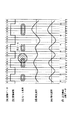
この実施形態において、データは、ゾーンCLV(ZCLV)方式で記録するものとする。このZCLV方式は、トラックをいくつかのゾーンに分割し、ゾーン内ではディスクの回転数を一定とする方式である。記録周波数は全周にわたって一定である。よって、同じゾーン内の各トラックの記録容量は等しい。図7においては、それぞれのゾーンに対するクロック信号は同一であり、各ゾーンに対する光ディスク1の回転数(速度)と1トラックずつのセクタ数とがそれぞれ異なったものとなっている。
【0038】
この実施形態において、“セクタ”という言葉は、記録、再生、書換えを行うことの出来る最小単位であるとする。DVDのファーマットにおいては、16個のセクタで1つのECCブロックが構成されている。DVDにおけるECCブロックの構成では、パリティが各セクタに分散して記録される。したがって、バイナリのデータ列としてはセクタ単位で書換えることが可能であるが、1セクタのみを書き換えたのではパリティに矛盾が生じてしまうため有意なデータとしてはECCブロック単位でしか書換えることは出来ないという事情がある。このことから、書換え単位はECCブロックであるという言い方も出来るが、この実施形態においては、バイナリのデータ列のアクセスが可能な単位である“セクタ”を記録可能な最小単位と呼ぶことにする。
【0039】
すなわち、上記光ディスク1は、図7に示すように、たとえば35個のゾーンからなり、それぞれのゾーンに対する光ディスク1の回転数(ゾーンごとの規準速度)と1トラックずつのセクタ数とがそれぞれ異なったものとなっている。
【0040】
各ゾーンは、半径方向に複数(1568)のトラックからなる。
【0041】
各ゾーンでは、光ディスク1の内周側から外周側に向かうのにしたがって、回転数(速度)が遅くなり、1トラックずつのセクタ数が増加するようになっている。
【0042】
上記各ゾーンのトラックには、図8に示すように、データの記録の単位としてのECC(error correction code )ブロックデータ単位(たとえば38688バイト)ごとに、データが記録されるようになっている。
【0043】
ECCブロックは、2Kバイトのデータが記録される16個のセクタからなり、各セクタごとにアドレスデータとしての4バイト(32ビット)構成のセクタID(識別データ)1〜ID16が2バイト構成のエラー検知コード(IED:IDエラーディテクションコード)とともにメインデータ(セクタデータ)に付与され、ECCブロックに記録されるデータを再生するためのエラー訂正コードとしての横方向のECC(error correction code )1と縦方向のECC2が記録されるようになっている。このECC1、2は、光ディスク1の欠陥によりデータが再生できなくなることを防止するために冗長語としてデータに付与されるエラー訂正コードである。
【0044】
各セクタは、172バイトで12行のデータにより構成され、各行(ライン)ごとに10バイト構成の横方向のECC1が付与されているとともに、182バイト構成の1行分の縦方向のECC2が付与されている。これにより、後述するエラー訂正部27は、横方向のECC1を用いて各ラインごとのエラー訂正処理を行うとともに、縦方向のECC2を用いて各列ごとのエラー訂正処理を行うようになっている。
【0045】
上記ECCブロックが光ディスク1に記録される際には、各セクタの所定のデータ量ごと(所定データ長さ間隔ごとたとえば91バイト:1456チャネルビットごと)にデータを再生する際にバイト同期を取るための同期コード(2バイト:32チャネルビット)が付与されている。
【0046】
各セクタは、図9に示すように、第0フレームから第25フレームの26個のフレーム(フレーム=91バイト:1456チャネルビット)から構成され、各フレームごとに付与されている同期コード(フレーム同期信号)が、フレーム番号を特定するための特定コード(1バイト:16チャネルビット)と、各フレーム共通の共通コード(1バイト:16チャネルビット)とから構成されている。
【0047】
図9は、DVDにおける物理セクタの構成である。32チャネルビットのSYNCコード(同期コード)から始まる26個のSYNCフレームで構成され、全体で38688チャネルビットとなっている。
【0048】
上記1セクタごとのフォーマットが、図10に示されている。
【0049】
図10において、1セクタは、2697バイト(bytes)で構成され、128バイトのヘッダ領域(ヘッダ部に対応)3、8、2バイトのミラー領域10、2567バイトの記録領域11から構成されている。
【0050】
上記セクタのヘッダ領域3、8に記録されるチャネルビットは、8−16RLL変調された形式になっており、上記セクタの記録領域11に記録されるチャネルビットは、1,7RLL変調された形式になっている。ヘッダ領域3、8にはマークポジション方式によりアドレスデータが記録されている。記録領域11には、マークエッジ方式によりユーザデータが記録されるようになっている。
【0051】
ヘッダ領域3、8は、光ディスク1を製造する際に所定のデータが記録されているエリアである。このヘッダ領域3、8は、4つのヘッダ1領域3a、8a、ヘッダ2領域3b、8b、ヘッダ3領域3c、8c、ヘッダ4領域3d、8dにより構成されている。
【0052】
ヘッダ1領域3a、8a〜ヘッダ4領域3d、8dは、46バイトあるいは18バイトで構成され、36バイトあるいは8バイトの同期コード部VFO(Variable Frequency Oscillator )、3バイトのアドレスマークAM(Address Mark)、4バイトのアドレス部PID(Position Identifier )、2バイトの誤り検知コードIED(ID Error Detection Code)、1バイトのポストアンブルPA(Postambles)により構成されている。
【0053】
ヘッダ1領域3a、8a、ヘッダ3領域3c、8cは、36バイトの同期コード部VFO1を有し、ヘッダ2領域3b、8b、ヘッダ4領域3d、8dは、8バイトの同期コード部VFO2を有している。
【0054】
同期コード部VFO1、2は、PLLの引き込みを行うための領域で、同期コード部VFO1はチャネルビットで“00010001…”の連続を“36”バイト(チャネルビットで576ビット)分記録(一定間隔のパターンを記録)したものであり、同期コード部VFO2はチャネルビットで“00010001…”の連続を“8”バイト(チャネルビットで128ビット)分記録したものである。同期コード部VFO1はいわゆる4Tの連続パターンとなっている。
【0055】
アドレスマークAMは、どこからセクタアドレスが始まるかを示す“3”バイトの同期コードであり、48ビットのチャネルコードとなっている。このアドレスマークAMの各バイトのパターンは“000100010000000000000100010001000000000000010001”というデータ部分には現れない特殊なパターンが用いられる。
【0056】
アドレス部PID1〜4は、4バイトのアドレスとしてのセクタ番号が記録されている領域である。セクタ番号は、光ディスク1のトラック上における物理的な位置を示す物理アドレスとしての物理セクタ番号であり、この物理セクタ番号はマスタリング工程で記録されるため、書き換えることはできないようになっている。
【0057】
上記アドレス部PID(1〜4)は、1バイト(8ビット)のセクタ情報と、3バイトのセクタ番号(トラック上における物理的な位置を示す物理アドレスとしての物理セクタ番号)から構成されている。セクタ情報は、2ビットのリザーブ領域、2ビットの物理ID番号領域、3ビットのセクタタイプ領域、1ビットのレイヤ番号領域により構成されている。
【0058】
物理ID番号は、例えばPID1の場合は“1”で、1つのヘッダ領域3、8で4回重ね書きしている内の何番目かを表す番号である。
【0059】
セクタタイプ領域には、トラックにおける最初のセクタ、最後のセクタ等を示すコードが記録されている。
【0060】
誤り検知コードIEDは、セクタアドレス(ID番号含む)に対するエラー(誤り)検知符号で、読み込まれたPID内のエラーの有無を検知することができる。
【0061】
ポストアンブルPAは、復調に必要なステート情報を含んでおり、ヘッダ領域51がスペースで終了するよう極性調整の役割も持つ。
【0062】
ミラー領域10は、トラッキングエラー信号のオフセット補正、ランド/グルーブ切り替え信号のタイミング発生等に利用される。
【0063】
記録領域11は、10〜11バイトのギャップ領域、20〜27のガード1領域、35バイトのVFO3領域、3バイトのプレ−シンクロナスコード(PS)領域、2418バイトのデータ領域、1バイトのポストアンブル3(PA3)領域、48〜55バイトのガード2領域、および24〜25バイトのバッファ領域により構成されている。
【0064】
ギャップ領域は、何も書かない領域である。
【0065】
ガード1領域は、相変化記録媒体特有の繰り返し記録時の終端劣化がVFO3領域にまで及ばないようにするために設けられた領域である。
【0066】
VFO3領域もPLLロック用の領域で、チャネルビットで“10001000…”の連続を“35”バイト(チャネルビットで560ビット)分記録するものである。
【0067】
PS(pre-synchronous code)領域は、データ領域につなぐための同調用の領域である。
【0068】
データ領域は、データID、データIDエラー検知コードIED(Data ID Error Detection Code)、同期コード、ECC(Error Correction Code )、EDC(Error Detection Code)、ユーザデータ等から構成される領域である。データIDは、各セクタの4バイト(32チャネルビット)構成のセクタデータである。データIDエラー検知コードIEDは、データID用の2バイト(16ビット)構成のエラー検知コードである。
【0069】
PA(post amble)3領域は、復調に必要なステート情報を含んでおり、前のデータ領域の最終バイトの終結を示す領域である。
【0070】
ガード2領域は、相変化記録媒体特有の繰り返し記録時の終端劣化がデータ領域にまで及ばないようにするために設けられた領域である。
【0071】
バッファ領域は、記録領域が次のヘッダ領域3、8にかからないように、光ディスク1を回転するモータの回転変動などを吸収するために設けられた領域である。
【0072】
ギャップ領域が、10から11バイトという表現になっているのは、ランダムシフトを行うからである。ランダムシフトとは相変化記録媒体の繰り返し記録劣化を緩和するため、データの書き始めの位置をずらすことである。ランダムシフトの長さは記録領域の最後尾に位置するバッファ領域の長さで調整され、1つのセクタ全体の長さは2697バイト一定である。
【0073】
次に、図11を用いて、上記ヘッダ領域3、8の他の実施形態について説明する。図10と同一部位には同一符号を付し説明を省略する。
【0074】
すなわち、ヘッダ領域3、8は、4つのヘッダ1領域3a’、8a’、ヘッダ2領域3b、8b、ヘッダ3領域3c’、8c’、ヘッダ4領域3d、8dにより構成されている。
【0075】
ヘッダ1領域3a’、8a’は、46バイトで構成され、先頭に6バイトの同期コード部VFOを配置し、この後、3バイトのアドレスマークAM、4バイトのアドレス部PID1、2バイトの誤り検知コードIED1、1バイトのポストアンブルPA1が4回繰返して記録されている構成となっている。
【0076】
ヘッダ3領域3c’、8c’は、46バイトで構成され、先頭に6バイトの同期コード部VFOを配置し、この後、3バイトのアドレスマークAM、4バイトのアドレス部PID3、2バイトの誤り検知コードIED3、1バイトのポストアンブルPA1が4回繰返して記録されている構成となっている。
【0077】
したがって、6バイトの同期コード部VFOの後にAM、PID、IED、PAの計10バイトを4回繰り返して記録するものである。これにより、PLLの引きこみ時間は専用のVFOパターン(36バイト)のみの場合より長くなるが、ヘッダ・フィールドのマージンが大きめであれば、繰り返し記録されたID情報を読める確率が上がるので、前述した図10の構成のものより有利になる。
【0078】
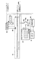
次に、上記光ディスク1を扱う光ディスク装置21について、図12を用いて説明する。
【0079】
上記光ディスク装置21は、光ディスク1を各ゾーンごとに異なった回転数で回転した状態で、上記光ディスク1に対してデータを記録したり、この光ディスク1に記録されているデータを再生するものである。
【0080】
上記光ディスク装置21の要部は、図12に示すように、光ピックアップ部(光学ヘッド)22、レベルスライス信号処理回路23、PRML信号処理回路24、信号判定回路25、ドライブ制御回路26は、エラー訂正部27、上位装置インターフェース28、変調器29、書込み補償回路30、書込みドライバ31、サーボ制御部32、スピンドルモータ33により構成されている。
【0081】
上記光ピックアップ部22は、対物レンズ34を有している。光ピックアップ22部内には、対物レンズ34に対応して半導体レーザユニット(図示せず)が設けられ、レーザ制御ユニットとしての書込みドライバ31によって付勢され、対応する波長のレーザ光を発生する。半導体レーザユニットが付勢されると、光ディスク1に対応するレーザ光が対応する対物レンズ34に向けられ、この対物レンズ34によって光ディスク1に収束される。この収束されたレーザ光で光ディスク1にデータが書き込まれ(マーク列の生成:可変長のマークとマークの間隔と、可変長の各マークの長さにより光ディスク1にデータが記録される)、或いは、再生される。
【0082】
書込みドライバ31は、書込み補償回路30によってその設定がセットされるが、その設定は、再生信号を得る再生パワー、データを記録する記録パワー及びデータを消去する消去パワーで異なっている。レーザ光は、再生パワー、記録パワー及び消去パワーの3つのパワーでそれぞれ異なるレベルのパワーを有し、それぞれのパワーのレーザ光が発生されるように半導体レーザユニットが書込みドライバ31によって付勢される。
【0083】
対物レンズ34に対向して光ディスク1が配置されるように、この光ディスク1は、直接或いはディスクカートリッジ(図示しない)に収納されてトレー(図示しない)によって装置内に搬送される。このトレーを駆動する為のトレーモータ(図示しない)が装置内に設けられている。また、装填された光ディスク1は、クランパー(図示しない)によって回転可能にスピンドルモータ33上に保持され、このスピンドルモータ33によって回転される。
【0084】
光ピックアップ部22は、信号検出部35を有している。この信号検出部35は、図13に示すように、レーザ光を検出する光検出器としてのフォトディテクタ40からの各検出信号(Ia、Ib、Ic、Id)をそれぞれ電流信号から電圧信号に変換するアンプ41a、41b、41c、41d、上記アンプ41a、41bからの信号を加算する加算器42a、上記アンプ41c、41dからの信号を加算する加算器42b、加算器42aからの信号を加算器42bからの信号により減算する減算器43により構成される。
【0085】
上記減算器43からの信号つまり信号検出部35からの出力信号は、ヘッダ領域3、8のデータの再生用のレベルスライス信号処理回路23と、記録領域11のデータの再生用のPRML信号処理回路24と、信号判定回路25とに出力される。
【0086】
また、アンプ81a、81b、81c、81dからの信号に基づいて、信号処理回路(図示しない)によりサーボ信号(トラックエラー信号、フォーカスエラー信号)を生成し、サーボ制御部32に出力される。
【0087】
フォーカスずれ量を光学的に検出する方法としては、たとえば次のようなものがある。
【0088】
[非点収差法] 光ディスク1の光反射膜または光反射性記録膜で反射されたレーザ光の検出光路に非点収差を発生させる光学素子(図示せず)を配置し、光検出器40上に照射されるレーザ光の形状変化を検出する方法である。光検出領域は対角線状に4分割されている。各検出領域から得られる検出信号に対し、信号処理回路(図示しない)内で対角和間の差を取ってフォーカスエラー検出信号(フォーカス信号)を得る。
【0089】
[ナイフエッジ法] 光ディスク1で反射されたレーザ光に対して非対称に一部を遮光するナイフエッジを配置する方法である。光検出領域は2分割され、各検出領域から得られる検出信号間の差を取ってフォーカスエラー検出信号を得る。
【0090】
通常、上記非点収差法あるいはナイフエッジ法のいずれかが採用される。
【0091】
光ディスク1はスパイラル状または同心円状のトラックを有し、トラック上に情報が記録される。このトラックに沿って集光スポットをトレースさせて情報の再生または記録/消去を行う。安定して集光スポットをトラックに沿ってトレースさせるため、トラックと集光スポットの相対的位置ずれを光学的に検出する必要がある。
【0092】
トラックずれ検出方法としては一般に、次の方法が用いられている。
【0093】
[位相差検出(Differential Phase Detection)法] 光ディスク1の光反射膜または光反射性記録膜で反射されたレーザ光の光検出器40上での強度分布変化を検出する。光検出領域は対角線上に4分割されている。各検出領域から得られる検出信号に対し、信号処理回路(図示しない)内で対角和間の位相差を取ってトラックエラー検出信号(トラッキング信号)を得る。
【0094】
[プッシュプル(Push-Pull )法] 光ディスク1で反射されたレーザ光の光検出器上での強度分布変化を検出する。光検出領域は2分割され、各検出領域から得られる検出信号間の差を取ってトラックエラー検出信号を得る。
【0095】
[ツインスポット(Twin-Spot )法] 半導体レーザ素子と光ディスク1間の送光系に回折素子などを配置して光を複数に波面分割し、光ディスク1上に照射する±1次回折光の反射光量変化を検出する。再生信号検出用の光検出領域とは別に+1次回折光の反射光量と−1次回折光の反射光量を個々に検出する光検出領域を配置し、それぞれの検出信号の差を取ってトラックエラー検出信号を得る。
【0096】
上記再生側の信号処理系は、ヘッダ領域3、8からの信号を検出遅延が少ないレベルスライス方式で処理する系(レベルスライス信号処理回路23)と、ユーザデータを記録する記録領域11からの信号を高密度記録が達成できるPRML信号処理方式で処理する系(PRML信号処理回路24)の2系統で構成されている。
【0097】
レベルスライス信号処理回路23は、図14に示すように、AGC(Automatic Gain Control)アンプ51、加算器52、等化器53、レベルスライス検出器54、PLL回路55、8−16RLL復調器56、AGC制御部57、オフセット制御部58により構成されている。
【0098】
AGCアンプ51は、信号検出器35からの信号のレベルをAGC制御部57からの制御信号により補正し、加算器52に出力するものである。加算器52はAGCアンプ51からの信号にオフセット制御部58からのオフセット信号を加算し、この加算結果を等化器53に出力するものである。
【0099】
等化器53は加算器52からの再生信号の波形(再生波形)に対して、等化波形とある設定された閾値との交点がウィンドウの中心になるような波形等化が施され、レベルスライス検出器54、AGC制御部57、オフセット制御部58に出力するものである。
【0100】
レベルスライス検出器54は、PLL回路55からのチャネルクロックに基づいて等化器53からの等化波形と閾値との交点を検出し、ウィンドウ内で交点が検出されれば「1」、検出されなければ「0」として2値データを8−16RLL復調器56へ出力するものである。
【0101】
PLL回路55は、レベルスライス検出器54からの信号に基づいてチャネルクロックが生成され、8−16RLL復調器56へ出力するものである。
【0102】
8−16RLL復調器56は、レベルスライス検出器54からの2値データを8−16RLLコードに基づいて復調するものである。
【0103】
AGC制御部57は、等化器53からの等化波形に基づいてAGCアンプ51における信号を補正するものである。
【0104】
オフセット制御部58は、等化器53からの等化波形に基づいて、オフセット値を加算器52へ出力するものである。
【0105】
上記レベルスライス信号処理回路23による信号処理方式として波形スライス方式について、図15の(a)〜(g)の動作波形図を用いて説明する。
【0106】
すなわち、光ディスク1には、記録すべき情報である図15の(a)に示す記録データに対応する図15の(b)に示すNRZI形式の記録波形に従って、図15の(c)に示すようにピット系列があらかじめ形成されている。
【0107】
このようにして光ディスク1に記録された情報を再生する場合、光ディスク1上に光ピックアップ部22内のフォトダイオードから再生用の光ビームが図15の(c)中に斜線で示すような微小なビームスポットとして照射され、ピット系列が読み出されることにより、再生信号が得られる。
【0108】
この再生信号の波形(再生波形)は、記録再生系の特性から図15の(b)の記録波形のような矩形波とはならず、図15の(d)に示すように鈍った波形として得られる。
【0109】
そこで、等化器53では再生波形に対して図15の(e)に示すように等化波形とある設定された閾値(一点鎖線で示す)との交点がウィンドウの中心になるような波形等化が施される。具体的には、再生信号の高周波成分の増幅が行われる。
【0110】
レベルスライス検出器54では、図15の(f)に示すように、等化波形と閾値との交点を検出し、ウィンドウ内で交点が検出されれば「1」、検出されなければ「0」として2値データを出力する。
【0111】
これにより、8−16RLL復調器56はレベルスライス検出器54からの2値データを復調するようになっている。
【0112】
PRML信号処理回路24は、図14に示すように、AGCアンプ61、加算器62、A/D変換器63、等化器(線形等化器)64、ML復号器(ヴィタビ復号器)65、1,7RLL復調器66、PLL回路67、AGC制御部68、オフセット制御部69により構成されている。
【0113】
AGCアンプ61は、信号検出器35からの信号のレベルをAGC制御部68からの制御信号により補正し、加算器62に出力するものである。加算器62はAGCアンプ61からの信号にオフセット制御部69からのオフセット信号を加算し、この加算結果をA/D変換器63に出力するものである。A/D変換器63は、PLL回路67からのチャネルクロックに基づいて、離散時間、離散振幅値系列に変換されてデジタル信号に変換し、等化器64へ出力するものである。
【0114】
等化器64は、FIRフィルタ(トランスバーサルフィルタ)からなる線形等化器で構成され、A/D変換器63からの再生信号の波形(再生波形)に対して、PR(1,1)特性の波形に等化する処理が施され、ML復号器65、PLL回路67、AGC制御部68、オフセット制御部69へ出力するものである。
【0115】
ML復号器65は、ヴィタビ復号器により構成され、等化器64からの等化波形を復号化し、バイナリデータとして検出され、1,7RLL復調器66へ出力するものである。
【0116】
1,7RLL復調器66は、ML復号器65からの復号化2値データを1,7RLLコードに基づいて復調するものである。
【0117】
PLL回路67は、等化器64からの信号に基づいてチャネルクロックが生成され、A/D変換器63へ出力するものである。すなわち、PR等化波形の振幅値と理想的な振幅値との差を位相差に換算することによりチャネルクロックをリカバリするものである。
【0118】
AGC制御部68は、等化器64からの等化波形に基づいてAGCアンプ61における信号を補正するものである。
【0119】
オフセット制御部69は、等化器64からの等化波形に基づいて、オフセット値を加算器62へ出力するものである。
【0120】
上記PRML信号処理回路24による信号処理方式について、図16の(a)〜(g)の動作波形図を用いて説明する。
【0121】
すなわち、光ディスク1には、記録すべき情報である図16の(a)に示す記録データに対応する図16の(b)に示すNRZI形式の記録波形に従って、図16の(c)に示すようにピット系列があらかじめ形成されている。
【0122】
このようにして光ディスク1に記録された情報を再生する場合、光ディスク1上に光ピックアップ部22内のフォトダイオードから再生用の光ビームが図16の(c)中に斜線で示すような微小なビームスポットとして照射され、ピット系列が読み出されることにより、再生信号が得られる。
【0123】
この再生信号の波形(再生波形)は、記録再生系の特性から図16の(b)の記録波形のような矩形波とはならず、図16の(d)に示すように鈍った波形として得られる。
【0124】
このような、図16の(d)の再生波形に対し、等化器64でPR(1,1)特性、PR(1,2,1)特性、PR(1,2,2,1)特性に基づく等化を行った場合の等化後の波形を図16の(e)(f)(g)にそれぞれ示す。PR(1,1)特性とは、インパルス応答が、連続する2識別点(=2つのチャネル・クロック時刻における再生波形の振幅値)に各々1:1の割合で現れる特性をいう。図16の(a)の記録データの最初の部分
0 1 0 0 1 0
に対応する図16の(b)のNRZI形式の記録波形は
0 1 1 1 0 0
となる。再生波形は、記録波形の1に対するインパルス応答と見なすので、
0 1 1 0
0 0 1 1 0
0 0 0 1 1 0
と言う応答の線形重畳として表される
0 1 2 2 1 0
という図16の(e)の波形が、PR(1,1)特性(クラス)として等化されるべき目標波形となる。
【0125】
PR(1,2,1)特性とは、インパルス応答が、連続する3識別点に各々1:2:1の割合で現れる特性をいう。PR(1,2,2,1)特性とは、インパルス応答が、連続する4識別点に各々1:2:2:1の割合で現れる特性をいう。PR(1,1)特性の場合と同様に、記録波形に対応するインパルス応答の線形重畳で求まる等化されるべき目標波形は、図16の(f)および図16の(g)となる。(図示しないが、他のPR特性についても同様である。)
このように、図16の(e)(f)(g)に示した通り、PR(1,1)特性→PR(1,2,1)特性→PR(1,2,2,1)特性の順に等化後の波形は鈍った特性になっていることが分かる。
【0126】
PRML方式では、再生波形の特性に近いPR特性へ波形等化することにより、等化器64での信号劣化成分の増加を抑制できる。
【0127】
一方、PRML方式の再生信号処理系において、等化器64の後に配置されるML復号器65には、最尤復号器の代表的な一つであるヴィタビ復号器が一般に用いられる。
【0128】
等化器64で再生波形がPR(1,2,2,1)特性へ等化されたとすると、ML復号器65は、PR(1,2,2,1)特性を満たす全ての再生波形系列の中から等化波形のサンプル系列との誤差が最も小さい系列を選択し、選択された再生波形系列を発生させる元となった記録データ(2値のデータ、復号データ)を、状態遷移を追いながら推定し、出力する。
【0129】
この様子を図17の(a)から(c)に示す。PRML方式では、復号を1つのサンプル値から行うのではなく、複数のサンプル値系列のPR特性による相関関係(波形干渉)を前提にしたシーケンスをもとに行うため、サンプル値間で相関を持たない信号劣化成分に対する耐性が強い。
【0130】
上記信号判定回路25は、再生中の信号がヘッダ領域3、8からの信号であるかユーザデータを記録する記録領域11からの信号であるかを判定するものである。
【0131】
上記信号判定回路25は、図13に示すように、バンドパスフィルタ(BPF)71、比較器(Comp)72、リトリガラブルマルチバイブレータ73により構成されている。なお、リトリガラブルマルチバイブレータ73には、抵抗R1、R2、コンデンサCからなる回路により電源電圧が供給されるようになっている。
上記信号判定回路25は、光ピックアップ部22の信号検出部35からの信号を入力して判定を行い、その結果をドライブ制御回路26に送る。
【0132】
例えば,ヘッダ領域3、8がプリピットで記録されて、ユーザデータの記録領域11がウォブルしているグルーブ2である場合、図13に示すようなフォトディテクタ40の
[(Ia+Ib)−(Ic+Id)]
の信号を、図13に示す信号検出器35に入力すると、図18の(d)に示した波形のようにユーザデータを記録する記録領域11に対応した判定信号を得ることができるので、これをもとにドライブ制御回路26は、記録領域11か否かの判定を行う。
【0133】
すなわち、バンドパスフィルタ(BPF)71は、図18の(a)に示すように、ウォブルしているグルーブ2に基づく振幅のある波形を比較器(Comp)72に出力する。比較器(Comp)72は、バンドパスフィルタ(BPF)71から振幅のある波形が供給された際に、図18の(b)に示す比較電圧V1に基づいて、図18の(c)に示すような、パルス信号をリトリガラブルマルチバイブレータ73に出力する。リトリガラブルマルチバイブレータ73は、比較器72からのパルス信号に基づいて、図18の(d)に示すような、判定信号をドライブ制御回路26に出力する。
【0134】
このように、図18の(a)に示すウォブル信号の凸部を比較器72で検出し、図18の(c)の検出信号をリトリガラブルマルチバイブレータ73のトリガ信号とすることで、ウォブル信号の凸部が検出されている間は、図18の(d)に示すように、リトリガラブルマルチバイブレータ73の出力が”1”の値をとる。
上記エラー訂正部27は、ECC復号器により構成され、上記レベルスライス信号処理回路23の8−16RLL復調器56からの復調データのエラー訂正を行って、ヘッダ領域3、8のデータとしてドライブ制御回路26へ出力したり、上記PRML信号処理回路24の1,7RLL復調器66からの復調データのECCのエラー訂正を行って、記録領域11からの再生データとして上位装置インターフェース28に出力する。
【0135】
上位装置インターフェース28は、上記エラー訂正部27からの再生データを上位装置(図示しない)に出力したり、上位装置からのアクセス位置及び記録、再生の指示をドライブ制御回路26に出力したり、上位装置からの記録データをECC符号化器(図示しない)により誤り訂正符号の付加されたデータ形式に変換してから変調器29に出力する。
【0136】
この変調器29は、上位装置インターフェース28から供給されるデータを1,7変調符号といった、チャネルに記録する為のデータに符号化され、記録補償器としての書込み補償回路30に出力する。書込み補償回路30は、変調器29からの出力波形をNRZI形式に変換するとともに、光ディスク1の熱伝導などに起因する書き込み波形とマーク形状とのずれを補償した書込み電流波形を書込みドライバ31に出力する。
【0137】
ドライブ制御回路26は、この光ディスク装置20の全体を制御するものである。
【0138】
ドライブ制御回路26は、信号判定回路25からの判定信号に基づいて、レベルスライス信号処理回路23またはPRML信号処理回路24に選択信号を送り、再生中のデータが適切に処理されるように制御を行うものである。
【0139】
たとえば、ドライブ制御回路26が、レベルスライス信号処理回路23の切換えスイッチ59に選択信号を出力することにより、切換えスイッチ59がオンし、8−16RLL復調器56からの復調データが切換えスイッチ59を介してエラー訂正部27に出力される。
【0140】
また、ドライブ制御回路26が、PRML信号処理回路24の切換えスイッチ70に選択信号を出力することにより、切換えスイッチ70がオンし、1,7RLL復調器66からの復調データが切換えスイッチ70を介してエラー訂正部27に出力される。
【0141】
また、ドライブ制御回路26は、上位装置からの指示データとエラー訂正部27からのデータによるアドレスデータに基づいて、サーボ制御部32を制御することにより、光ピックアップ部22による光ビームをアクセス位置に移動制御するとともに、スピンドルモータ33をアクセス位置に対応するゾーンの回転数に制御するようになっている。
【0142】
また、ドライブ制御回路26は、書込みドライバ31を制御することにより、書込み補償回路30からの記録データに基づいて、半導体レーザ発振器(図示しない)を制御することにより、光ビームを発生するようになっている。
【0143】
また、ドライブ制御回路26は、AM検出器26a、SYNC検出器26b、フォーマットコントローラ26cを有している。
AM検出器26aは、レベルスライス信号処理回路23のPLL回路55からのチャネルクロックに基づいて、8−16RLL復調器56からの復調信号によりヘッダ領域3、8のアドレスマークAMを検出するものである。
たとえば、アドレスマークAMのパターンを記憶しているレジスタと、8−16RLL復調器56からの復調信号をPLL回路55からのチャネルクロックに基づいて記録するレジスタと、上記2つのレジスタのレジストデータを比較する比較器とを有し、比較器により一致信号が出力された際、アドレスマークAMの検出信号としてフォーマットコントローラ26cに出力されるものである。
【0144】
SYNC検出器26bは、PRML信号処理回路24のPLL回路67からのチャネルクロックに基づいて、1,7RLL復調器66からの復調信号により記録領域11のSYNCコードを検出するものである。
たとえば、SYNCコードのパターンを記憶しているレジスタと、1,7RLL復調器66からの復調信号をPLL回路67からのチャネルクロックに基づいて記録するレジスタと、上記2つのレジスタのレジストデータを比較する比較器とを有し、比較器により一致信号が出力された際、SYNCコードの検出信号としてフォーマットコントローラ26cに出力されるものである。
【0145】
フォーマットコントローラ26cは、AM検出器26aからのアドレスマークAMの検出信号、SYNC検出器26bからのSYNCコードの検出信号で同期を取りながら、リードクロック、ライトクロックまたはウォーブルクロックを計数することにより、光ピックアップ部22からのレーザ光のトラック上での照射位置を判別し、この判別結果を基準として各部に出力する制御信号のタイミングを制御するようになっている。
上記リードクロックは、データ再生(読出し)時のクロックであり、ヘッダ領域3、8の再生時、PLL回路55からのチャネルクロックがフォーマットコントローラ26cに供給され、記録領域11の再生時、PLL回路67からのチャネルクロックがフォーマットコントローラ26cに供給される。
上記ライトクロックは、図示しないクロック生成部からの一定周期のクロックつまり発振器からの基準クロックに基づいて生成されるクロックであり、フォーマットコントローラ26cに供給される。
【0146】
上記ウォーブルクロックは、光ピックアップ部22の信号検出部35からの出力信号に基づいて図示しないクロック生成部により生成されるクロックであり、フォーマットコントローラ26cに供給される。
すなわち、フォーマットコントローラ26cは、記録領域11のデータの読出し時にあっては、ヘッダ領域3、8のアドレスマークAMの検出信号、記録領域11のSYNCコードの検出信号で同期を取りながら、リードクロック、またはウォーブルクロックを計数することにより、光ピックアップ部22からのレーザ光のトラック上での照射位置を判別し、この判別結果を基準として各部に出力する制御信号のタイミングを制御するようになっている。
また、フォーマットコントローラ26cは、記録領域11のデータの書込み時にあっては、ヘッダ領域3、8のアドレスマークAMの検出信号で同期を取りながら、ヘッダ領域3、8においては、リードクロック、またはウォーブルクロックを計数し、記録領域11においては、ライトクロック、またはウォーブルクロックを計数することにより、光ピックアップ部22からのレーザ光のトラック上での照射位置を判別し、この判別結果を基準として各部に出力する制御信号のタイミングを制御するようになっている。
上述した図13、図14の構成において、ヘッダ領域3、8はプリピットであるので、書きこみデータの変調器29は、記録領域11のPRML方式で使用する(1,7)RLL符号にだけ対応していれば良い。
【0147】
再生側の信号処理系は、ヘッダ領域3、8をレベルスライス方式で処理する系と、ユーザデータを記録する記録領域11をPRML信号処理方式で処理する系の2系統で構成されているが、上記実施形態では、ヘッダ領域3、8の変調方式には最短ラン長が3である8−16変調が用いられているため、レベルスライス方式の信号処理系の後段には8−16RLL変調符号の復調器56が必要になる。また、ユーザデータを記録する記録領域11の変調方式には最短ラン長が1である(1,7)変調が用いられているため、PRML方式の信号処理系の後段には(1,7)RLL変調符号の復調器66が必要になる。
【0148】
図19は、PRML信号処理回路24の主要構成要素である、線形の等化器(PR等化器)64とML復号器(ヴィタビ復号器、ML検出器)65の構成をより詳細に示した図である。
【0149】
ML復号器65は、等化波形のサンプル系列との誤差が最も小さい系列を選択し、選択された系列に対応する2値データ(復号データ)を出力する。
【0150】
即ち、図17の(a)〜(c)に示したように、PR(1,2,2,1)等化後の信号波形系列が、
0 1 3 5 5 3 1 1 3 5 6 5 3 1……
であった場合、記録されたデータの候補
0 1 0 1 0 …… ( 記録波形は、 0 1 1 0 0……)
に対応するインパルス応答、
0 1 2 2 1 0 ……
0 0 1 2 2 1 ……
の線形重畳でえられる理想的なPR特性の再生波形である
0 1 3 4 3 1 ……
や、
他の記録されたデータの候補
0 1 1 1 0…… ( 記録波形は、 0 1 1 1 0……)
に対応するインパルス応答、
0 1 2 2 1 0 0 ……
0 0 1 2 2 1 0 ……
0 0 0 1 2 2 1 ……
の線形重畳でえられる理想的なPR特性の再生波形である
0 1 3 5 5 3 1 ……
等の波形系列との相互相関を計算し、再生等化波形との相関の最も大きい(=系列間の誤差の最も小さい)系列を、確率的手法により選択する。
【0151】
波形の候補は、ツリー構造状に増加するような数え上げもできるが、PR特性を考慮すると取り得る状態数は有限となる。PR(1,2,2,1)特性の場合は、拘束長(波形干渉が及ぶ範囲)は4であり、波形干渉に起因する記録データ系列のバリエーションは 0か1の2通りのデータ値が4つ並ぶ組み合わせの16通りであるから、冗長のない状態数は最大でも16である。変調符号の制限が入るとさらにこの状態数が減る可能性が有る。
【0152】
ML復号器65では、入力されたサンプル値にしたがって、有る状態から次の状態に遷移したと仮定した場合の確率を計算する。同じ状態へ遷移する波形系列の候補が複数になった場合、どちらの候補を選んだほうが確からしいかを過去からの遷移確率の累積値で判断する。
【0153】
この為、ML復号器65には、波形系列の候補を記憶する為のパスメモリ65dが存在する。通常この長さは、数十チャネルビット分に設定される。波形系列の候補は、パスメモリ65dを通過する内に、複数候補が同じ状態に遷移することによる選択が繰り返され、最終的に最も確からしい系列が選択される。
【0154】
ブランチメトリック計算部65aとは、サンプル値が入力された時に、有る状態から次の候補の状態移ったと推定される場合の理想振幅値との誤差から換算される、状態が遷移する確率の対数値を計算するものである。パスメトリックメモリ65cとは、状態数の各々の状態に対して、状態遷移が繰り返されてその状態になるまでの過去のブランチメトリックの積算値用のメモリである。
【0155】
ACS65bとは、Add(加算) Compare(比較) Select(選択) 操作を行う回路の略称である。図20に示すように、時刻1における状態Aのパストリック値が5、状態Bが8、時刻2で状態Aから状態Aに遷移するブランチメトリックが4、状態Aから状態Bに遷移するブランチメトリックが5、状態Bから状態Aに遷移するブランチメトリックが2、状態Bから状態Bに遷移するブランチメトリックが5であると仮定する。ACS65bでは、時刻1における状態Aのパストリック値5と状態Aから状態Aに遷移するブランチメトリック4とを加算した値9と、時刻1における状態Bのパストリック値8と状態Bから状態Aに遷移するブランチメトリック2とを加算した値10とを比較し、値の大きい状態Bから状態Bへの遷移を選択する。(実際には値の大きいほうを選択ようにするとメトリック値が発散するので、数式の操作により、確率の大きい遷移のメトリック値が小さな値となるような計算を行い、メトリック値の小さいほうが選択される回路として実装され場合が多い)同様に、時刻1における状態Aのパストリック値5と状態Aから状態Bに遷移するブランチメトリック5とを加算した値10と、時刻1における状態Bのパストリック値8と状態Bから状態Bに遷移するブランチメトリック5とを加算した値13とを比較し、値の大きい状態Bから状態Bへの遷移を選択する。この場合、時刻2の各状態に遷移したのは、時刻1の状態Bだけであるから、時刻1に状態Aとなる波形系列は、選択される候補からはずれる。パスメモリ65dは、選択されて候補に残った系列(=パス)を記録する為のメモリである。通常、パスメモリ65dを通過するまでには、1つの系列しか残らないが、ノイズの状態によっては、複数の系列が候補として残る場合もあり、その場合には、パス選択部65eによりパスメモリ65dの内容とパスメトリックメモリ65cのパスメトリックとを比較して最も確からしいと判断されるほうが選択される。
【0156】
系列の選択が行われて検出データが確定するのは、このようにパスメモリ66dを通った後なので、ML復号器65の出力は、従来の波形スライス方式のデータ検出器に比べて遅延が大きい。
【0157】
上記実施形態では、ヘッダ領域3、8は、検出遅延が少ないレベルスライス方式でデータが検出され、ユーザデータの記録領域11は高記録密度が達成できるPRML方式でデータが検出される。PRML方式の場合、コードレートが高くチャネルの帯域を低く押さえることのできる1,7変調方式のような方式が用いられる。
【0158】
1,7変調は、コードレートが2/3、データ系列中の“1”と“1”の間に“0”が最低いくつ入るかを示す最短ラン長(minimum run length)(=d制約)が1、データ系列中の“1”と“1”の間に“0”が最大いくつ入るかを示す最長ラン長(maximum run length)(=k制約)が7であるようなコードへの変換方式である。
【0159】
PRML方式に適するコードレートが2/3(2対3、2ビットデータを3ビットに変換)の変調方式には、1,7変調のほかに、d制約が同じく1である、8−12変調等がある。
【0160】
これに対して,レベルスライス方式の場合は、コードレートは低いが、最短ラン長を大きく取ることのできる2,7変調方式のような方式が向いている。2,7変調は、コードレートが1/2、データ系列中の“1”と“1”の間に“0”が最低いくつ入るかを示す最短ラン長(minimum run length)(=d制約)が2、データ系列中の“1”と“1”の間に“0”が最大いくつ入るかを示す最長ラン長(maximum run length)(=k制約)が7 であるようなコードへの変換方式である。レベルスライス方式に適する最短ラン長(minimum run length)(=d制約)が2の変調方式には、2,7変調のほかに、コードレートが8/16である8−16変調や、コードレートが8/15である8−15変調等がある。
【0161】
最短ラン長を大きく取ることのできる方式がレベルスライス方式に向いている理由は、PRML方式の場合、最短マーク/ピットの振幅値は小さくても線形重畳性が成り立っていることが重要であるのに対して、レベル・スライスでは、最短マーク/ピットにおいても振幅値がある程度以上ないとレベルでスライスできない為である。
【0162】
1,7変調は、コードレートが 2/3 で、d制約が1、k制約が7の変調コードである。d制約が1とは、図21の(a)に示したように、変調後のコードに現れる1と1の間に最低1個の0が含まれるような制限が設けられていることを示す。k制約が7とは、変調後のコードに現れる1と1の間に最大7個までしか0が含まれないような制限が設けられていることを示す。光ディスク1上に記録されるときには、変調されたコードがNRZI形式で記録されるので(図21の(b))、最短ピット/マーク長は2チャネルクロック、最大ピット/マーク長は8チャネルクロック分の長さになる。
【0163】
DVDで採用されている8−16変調は、コードレートが1/2で、d制約が2、k制約が10の変調コードである。よって、媒体上に記録されるときには、最短ピット/マーク長は3チャネルクロック、最大ピット/マーク長は11チャネルクロック分の長さになる。8−15変調も8−16変調と同じく、d制約が2で最短ピット/マーク長は3チャネルクロック分の長さである。
【0164】
ここで、仮にユーザデータ記録密度を、1,7変調と8−16変調で等しくするとすると、1,7変調は2ビットのユーザデータを3ビットのコードに変換し、8−16変調は2ビットのユーザデータを4ビットのコードに変換するので、1チャネルクロックの長さは、8−16変調が1,7変調の3/4になる。ただし、8−16変調の最短ピット/マーク長は3チャネルクロックで、1,7変調の最短ピット/マーク長は2チャネルクロックなので、トータルとしては、
3/4 * 3/2 = 9/8
となり、ピットの長さが若干8−16変調のほうが長く、レベルスライスに有利な状態になっていることがわかる。したがって、ヘッダ領域3、8で検出遅延の少ないレベルスライス方式を使用するには、ヘッダ領域3、8に記録する情報の線方向の記録密度を、ユーザデータの記録領域11の線方向の記録密度よりも低くしなければならない。
【0165】
上述の例では、より現実に即したコードの選択例として、ヘッダ領域3、8に8−16変調、ユーザデータの記録領域11に1,7変調を使用した場合について説明したが、場合によっては、変調コードをヘッダ領域3、8とユーザデータの記録領域11で同じにしても構わない。この場合も、ユーザデータの記録領域11にPRMLを使用するほどの記録密度においては、PRMLと同じ振幅値でレベルスライス方式を動かすことはできないので、ヘッダ領域3、8の線方向の記録密度を下げてピット/マーク長を大きくして振幅値を稼がなければならない。
【0166】
変調コードをヘッダ領域3、8とユーザデータの記録領域11で同じにし、ヘッダ領域3、8の線方向の記録密度を下げてピット長あるいはマーク長を大きくして振幅値を稼ぐ方法の一例に、最短ピット長のコードが現れないようにしたデータをヘッダ領域3、8に書きこむ方法がある。
【0167】
この方法の利点は、物理的なピットの記録密度は下がるがチャネルクロックレートが、ヘッダ領域3、8とユーザデータの記録領域11で同じになる点である。したがって、クロックリカバリの為のPLLをヘッダ領域3、8の為のものと、ユーザデータの記録領域11の為のものとに分ける必要がなくなる。また、変調コードも同じであるから復調器も共用することができる。
【0168】
ヘッダ領域3、8にプリピットヘッダを用いた録再型の光ディスク装置では、ユーザデータの記録領域11のマークからの信号とヘッダ領域3、8のピットからの信号にはレベルに大きな差がある。PRML信号処理方式は、チャネルクロックに同期した識別点での振幅値を検出する方式なので、レベルの変動に弱い。ヘッダ領域3、8とユーザデータの記録領域11の間でのAGCによるレベルの補正は当然行われるが、検出系が同じPRML信号処理方式を使用している場合、切り替え時点での前のレベルの影響を完全に除去するのは難しい。
【0169】
また、影響が殆ど無いようにするには、切替用のGAPフィールドを大きく取らなければならないのでフォーマット効率が低下する。プリピットヘッダを用いる録再型光ディスクの場合にID部に従来のレベルスライスを適用するとこれらの改善効果も見込まれる。
【0170】
また、上記ヘッダ領域3、8においては、図22の(a)〜(c)に示すように、最短ピット(マーク)長が3チャネルクロックである変調コードで記録されており、上記記録領域11においては、図22の(d)〜(f)に示すように、最短ピット(マーク)長が2チャネルクロックである変調コードで記録されている。
【0171】
すなわち、図22の(a)〜(c)は、(1,7)変調における最短ピットの場合のチャネルビットパターン(図22の(a))、書込み電流波形(図22の(b))、書込まれるピット(マーク)(図22の(c))の関係を示している。
【0172】
図22の(d)〜(f)は、8−16変調における最短ピット(マーク)の場合のチャネルビットパターン(図22の(d))、書込み電流波形(図22の(e))、書込まれるピット(マーク)(図22の(f))の関係を示している。
【0173】
図22の(d)〜(f)に示した8−16変調のようにコードレートの低い変調方式では、最短ピット/マーク長が長い場合でも、クロック周波数が高くなって、データの検出ウインドウ幅が狭くなる。
8−16変調の場合、比率で言うと、1ビットのユーザデータを2ビットのチャネルビットパターンに変換しているのに対して、よりコードレートの高い(1,7)変調の場合、2ビットのユーザデータを3ビットのチャネルビットパターンに変換している。
【0174】
したがって、図22の(a)〜(c)と図22の(d)〜(f)に示した関係のように、最短ピット(マーク)長は8−16変調の方が長く、その分(1,7)変調より振幅が大きく取れる場合でも、ウインドウ幅は(1,7〉変調より8−16変調の方が短くなり、波形の立ち上りと立下り位置の制御が厳しくなる。
【0175】
記録密度をつめる場合に、最短ピット/マーク長で制限される条件では、両端に情報を持たせることの出来るマークエッジ方式の方が有利であるが、記録密度を下げてマージンを稼ぐ方向では、マークの位置のみに情報を持たせるマークポジション方式の方がデータの記録および再生手段の構成を簡略化することで信頼性の向上が見込まれる。
【0176】
すなわち、ヘッダ領域3、8は、マークポジション方式の記録方法でプリピットが形成されていて、ユーザデータが記録される記録領域11では、マークエッジ方式の記録方法により記録マークが書込まれる。
【0177】
図2に示すように、グルーブ記録方式の場合でも、ヘッダ領域3のプリピットヘッダの部分ではグルーブが途切れる場合がある。
【0178】
また、図4に示すように、グルーブ/ランド記録方式の場合でも、ヘッダ領域8のプリピットヘッダの部分ではグルーブが途切れる場合がある。
【0179】
すなわち、グルーブを半径方向にウォブリングさせるウォブル・グルーブ方式の場合、ウォブルに同期させたクロックでタイミングを生成しているので、ウォブル・グルーブが途切れる前と再開した時点でクロックの位相に対してずれがあるとPLLの再引きこみが必要になるため安定性が損なわれる。
【0180】
したがって、ヘッダ領域3、8と記録領域11で記録密度や最短ピット/マーク長を変えた場合でも、ヘッダ領域3、8のグルーブが途切れる長さはグルーブ周期の整数倍とする。または、ヘッダ領域3、8後のウォブル・グルーブの再開時点の振幅の位相を、終了時点の位相とヘッダ領域3、8による中断時間から求めることのできる値となっている。
【0181】
即ち、中断前のウォブル信号に同期していたPLL回路55、67の位相差検出回路(図示しない)の出力が、中断後のウォブル信号が入力された時点でも、大きな位相差を検出しないような位相となっている。
【0182】
記録密度を下げて(粗)ピット/マーク長を大きくすれば、確かに振幅値を稼ぐことはできるが、レベルスライス方式の場合、振幅値と並んで重要なのは検出ウィンドウ幅である。
【0183】
DVDにおいては、光ディスク1へのピット/マークの記録方式は、波形の立ち上りと立下りの位置に情報を持たせたマークエッジ方式である。図22の(b)に示すように、8−16変調のようなコードレートの低い変調方式では、最短ピット/マーク長が長い場合でも、クロック周波数が高くなって、データの検出ウィンドウ幅が狭くなる。即ち、波形の立ち上りと立下り位置の制御が厳しくなる。記録密度をつめる(密)場合に、最短ピット/マーク長で制限される条件では、両端に情報を持たせることのできるマークエッジ方式の方が有利であるが、記録密度を下げてマージンを稼ぐ方向では、マークの位置のみに情報を持たせるマークポジション方式の方がデータの記録および再生手段の構成を簡略化することで信頼性の向上が見込まれる。
【0184】
即ち、図2、図4において、ヘッダ領域3、8は、マークポジション方式の記録方法でプリピットが形成されていて、ユーザデータの記録領域11では、マークエッジ方式の記録方法により記録マークが書きこまれる。
【0185】
次に、上記のような構成において、上記光ディスク装置21におけるデータの記録処理、データの再生処理について、図23のフローチャートを参照しつつ説明する。
【0186】
すなわち、光ピックアップ部22のシーク直後、あるいはフォーマットコントローラ26cが外乱等により追従から外れた際、つまりフォーマットコントローラ26cがトラック上の位置を把握することができなくなった際に、以下の制御が行われる。
【0187】
すなわち、信号判定回路25は、光ピックアップ部22から供給される信号の信号レベルを調べ(ST1)、ユーザデータを記録する記録領域11か否かを判定する(ST2)。
【0188】
これにより、信号判定回路25は、ユーザデータを記録する記録領域11を判定した際、ユーザデータを記録する記録領域11を示す信号をドライブ制御回路26に出力する(ST3)。
【0189】
この結果、ドライブ制御回路26は、PRML信号処理回路24に選択信号を出力する(ST4)。
【0190】
また、上記ステップ2において、信号判定回路25は、ユーザデータを記録する記録領域11を判定しなかった際、ヘッダ領域3、8を示す信号をドライブ制御回路26に出力する(ST5)。
【0191】
この結果、ドライブ制御回路26は、レベルスライス信号処理回路23に選択信号を出力する(ST6)。
【0192】
上記ステップ4あるいはステップ6による選択信号によりPRML信号処理回路24あるいはレベルスライス信号処理回路23が選択されている状態において、ドライブ制御回路26は、フォーマットコントローラ26cの同期を取り、領域ごとに適切な信号処理系からのデータに基づいて、データの記録あるいは記録されているデータの再生を行う(ST7)。
【0193】
なお、データが正常に再生され始めるとフォーマットコントローラ26cがトラック上の位置を把握することが可能となり、信号判定回路25による判定結果は使用されなくなる。
【0194】
上記実施形態では、信号判定回路25が、光ピックアップ部22の後段に設けられている場合について説明したが、これに限らず、図24に示すように、エラー訂正部27の後段に信号判定回路36が設けられている場合も上記同様に実施できる。図12と同一部位には同一符号を付し説明を省略する。
【0195】
この信号判定回路36は、データが有意であるかどうかで再生中の信号がヘッダ領域3、8からの信号であるかユーザデータを記録する記録領域11からの信号であるかを判定する。ヘッダ領域3、8からの信号であるかユーザデータを記録する記録領域11からの信号であるかを判定するため、初期状態においてはどちらかの領域であると仮定してデータの読出しを試みる。信号が仮定した方の領域からのものになった時点で、同期コード部VFO、アドレスマークAMといった有意なデータが得られるので、その時点で仮定した領域内の位置を検出する。
【0196】
書換え型の場合、ユーザデータを記録する記録領域11にはデータが書かれていない場合もあり得るので、ヘッダ領域3、8を仮定して有意データのサーチを行う方が良い。
【0197】
この場合、信号判定回路36は、光ピックアップ部22からの信号を処理したレベルスライス信号処理回路23の出力に基づくエラー訂正部27からの出力に基づいて、ヘッダ領域3、8のデータが読取れるか否かを判断し、ヘッダ領域3、8のデータが読取れた際に、ヘッダ領域3、8を判定するものである。
【0198】
上記構成において、上記光ディスク装置21におけるデータの記録処理、データの再生処理について、図25のフローチャートを参照しつつ説明する。
【0199】
すなわち、光ピックアップ部22のシーク直後、あるいはフォーマットコントローラ26cが外乱等により追従から外れた際、つまりフォーマットコントローラ26cがトラック上の位置を把握することができなくなった際に、以下の制御が行われる。
【0200】
すなわち、信号判定回路36は、ヘッダ領域3、8を示す信号をドライブ制御回路26に出力する(ST11)。
【0201】
この結果、ドライブ制御回路26は、レベルスライス信号処理回路23に選択信号を出力する(ST12)。
【0202】
これにより、レベルスライス信号処理回路23からの信号がエラー訂正部27を介して信号判定回路36に供給される。
【0203】
この結果、信号判定回路36は、同期コード部VFO、アドレスマークAMといった有意なデータが得られるか否かを判定する(ST13)。
【0204】
これにより、信号判定回路36は、有意なデータが得られた際、ヘッダ領域3、8を示す信号をドライブ制御回路26に出力する(ST14)。
【0205】
この結果、ドライブ制御回路26は、フォーマットコントローラ26cの同期を取り、領域ごとに適切な信号処理系からのデータに基づいて、データの記録あるいは記録されているデータの再生を行う(ST15)。
【0206】
なお、データが正常に再生され始めるとフォーマットコントローラ26cがトラック上の位置を把握することが可能となり、信号判定回路36による判定結果は使用されなくなる。
【0207】
次に、図26、図27を用いて、他の実施形態について説明する。この場合、図12、図14と同一部位には同一符号を付し説明を省略する。
【0208】
この実施形態では、変調コードをヘッダ領域3、8とユーザデータを記録する記録領域11で同じにし、最短ピット長のコードが現れないようにしたデータをヘッダ領域3、8に書きこむことで、ヘッダ領域3、8の線方向の記録密度を下げて(粗として)ピット/マーク長を大きくして振幅値を稼ぐ場合の光ディスク装置21の構成図の一例を示す。
【0209】
再生側の信号処理系は、ヘッダ領域3、8をレベルスライス方式で処理してチャネルデータを検出する系(レベルスライス信号処理回路23’)と、ユーザデータを記録する記録領域11をPRML信号処理方式で処理してチャネルデータを検出する系(PRML信号処理回路24’)の2系統で構成されている。
【0210】
図27の場合、レベルスライス信号処理回路23’は、図14に示す、レベルスライス信号処理回路23からPLL回路55、8−16RLL復調器56を除去した構成となっており、PRML信号処理回路24’は、図14に示す、PRML信号処理回路24からPLL回路67、1,7RLL復調器66を除去した構成となっている。
【0211】
図26の場合、レベルスライス信号処理回路23’とPRML信号処理回路24’とが共通に用いるPLL回路37と復調器38が設けられている。
【0212】
また、ドライブ制御回路26は、信号判定回路25からの判定信号に基づいて、レベルスライス信号処理回路23’またはPRML信号処理回路24’に選択信号を送り、再生中のデータが適切に処理されるように制御を行うものである。
【0213】
また、この際、ドライブ制御回路26は、信号判定回路25からの判定信号に基づいて、PLL回路37内の位相差検出回路37aに位相差の検出方式の切替信号を送り、再生中のデータが適切に処理されるように制御を行うものである。これにより、PLL回路37の位相差検出回路37aはレベルスライス信号処理回路23’またはPRML信号処理回路24’に適した位相差の検出方式(レベルスライス方式の位相差の検出またはPRML方式の位相差の検出)で位相差が検出されている状態で再生用のクロックが生成される。
【0214】
この結果、チャネルデータが検出された後は共通の復調器38で復調される。
【0215】
次に、上記のような構成において、上記光ディスク装置21におけるデータの記録処理、データの再生処理について、図28のフローチャートを参照しつつ説明する。
【0216】
すなわち、光ピックアップ部22のシーク直後、あるいはフォーマットコントローラ26cが外乱等により追従から外れた際、つまりフォーマットコントローラ26cがトラック上の位置を把握することができなくなった際に、以下の制御が行われる。
【0217】
すなわち、信号判定回路25は、光ピックアップ部22から供給される信号の信号レベルを調べ(ST1)、ユーザデータを記録する記録領域11か否かを判定する(ST2)。
【0218】
これにより、信号判定回路25は、ユーザデータを記録する記録領域11を判定した際、ユーザデータを記録する記録領域11を示す信号をドライブ制御回路26に出力する(ST3)。
【0219】
この結果、ドライブ制御回路26は、PRML信号処理回路24’と位相差検出回路37aに選択信号を出力する(ST4’)。
【0220】
また、上記ステップ2において、信号判定回路25は、ユーザデータを記録する記録領域11を判定しなかった際、ヘッダ領域3、8を示す信号をドライブ制御回路26に出力する(ST5)。
【0221】
この結果、ドライブ制御回路26は、レベルスライス信号処理回路23と位相差検出回路37aに選択信号を出力する(ST6’)。
【0222】
上記ステップ4’あるいはステップ6’による選択信号によりPRML信号処理回路24あるいはレベルスライス信号処理回路23が選択されている状態において、ドライブ制御回路26は、フォーマットコントローラ26cの同期を取り、領域ごとに適切な信号処理系からのデータに基づいて、データの記録あるいは記録されているデータの再生を行う(ST7)。
【0223】
なお、データが正常に再生され始めるとフォーマットコントローラ26cがトラック上の位置を把握することが可能となり、信号判定回路25による判定結果は使用されなくなる。
【0224】
次に、図29を用いて、他の実施形態について説明する。上述した実施形態では、ヘッダ領域3、8が4つのヘッダフイールドからなり、各ヘッダフイールド内のアドレス部PIDの手前に1つだけアドレスマークAMが設けられていたが、これに限らず、他の実施形態としては、1つのヘッダフイールド内に複数のアドレスマークAMが設けられているものであっても良い。
【0225】
図29にヘッダフィールド71のレイアウトを示す。上述したヘッダ領域3、8のフォーマットでは、ヘッダフィールドは4つあるが、ここでは簡単の為に、ヘッダフィールド71は一つであると仮定するが、ヘッダフィールド71の数を限定するものではない。
【0226】
このヘッダフィールド71は、データの区切りを検出するためのパターンであるAM(Address Mark)パターンが、同一のヘッダフィールド71の複数箇所に記録されている所に大きな特徴がある。
【0227】
ヘッダフィールド71は、49バイトで構成され、左から順に、36バイトの同期コード部VFO(Variable Frequency Oscillator )、3バイトのアドレスマークAM(Address Mark)、4バイトのアドレス部PID(Position Identifier )、2バイトの誤り検知コードIED(ID Error Detection Code)、1バイトのポストアンブルPA(Post ambles)、3バイトのアドレスマークAM(Address Mark)により構成されている。
【0228】
これにより、ヘッダフィールド71に記録された情報の再生時の信頼性を大幅に向上させることができる。すなわち、この実施形態では、図29に示したように、データのバイト同期を取るためのアドレスマークAMがアドレス部PIDの前とポストアンブルPAの後ろにある。
【0229】
通常は、アドレス部PIDの前のアドレスマークAMで同期を取って、以後の情報を切り出し、エラー検出コードでエラーが検出されなければ、正しいセクタ情報、セクタ番号が得られたものとする。
【0230】
この実施形態においては、エラー検出コードでエラーが検出されても、アドレス部PIDの前のアドレスマークAMのみの検出誤りである場合には、以下に示すような手段により、正しいセクタ情報、セクタ番号が得られる。アドレス部PID前のアドレスマークAMは、同期コード部VFOの直後に位置しているため、何らかの外乱によりPLLの引きこみが遅れた場合には検出誤りになり易い。しかし、そのような場合でもアドレス部PID以降のデータは正常に読み出されている場合がある。
【0231】
次に、上記した1つのヘッダフィールド71内に2つのアドレスマークAMを持つ場合における、アドレス部PIDを検出するID検出回路80を、図30、図31を用いて説明する。
【0232】
図30は、ID検出回路80の回路構成例であり、図31は、このID検出回路80を搭載した光ディスク装置21の回路構成例である。図31の場合、図12、図14と同一部位には同一符号を付し説明を省略する。ただし、信号判定回路25とレベルスライス信号処理回路23内の切換えスイッチ59とPRML信号処理回路24内の切換えスイッチ70が除去されている。
【0233】
上記ID検出回路80は、図31に示すように、ヘッダ領域からの信号を処理するレベルスライス信号処理回路23の最終段である8−16RLL復調器56の後段に設けられ、8−16RLL復調器56により復号されたバイナリデータとPLL回路55からのチャネルクロックに基づいてID情報を検出し、ドライブ制御回路26に出力するものである。
【0234】
上記ID検出回路80は、図30に示すように、シフトレジスタ81、アドレスマーク検出器(AM検出器)82、カウンタ83、ID情報検出器84、スタックレジスタ85、切換えスイッチ86a、86b、スタックカウンタ87により構成されている。
【0235】
シフトレジスタ81は、8−16RLL復調器56により復号されたバイナリデータとしてのチャネルビットデータが入力端81aから入力され、このチャネルビットデータをチャネルクロックに同期して1ビットずつ図の左方向にシフトして行くものである。シフトレジスタ81の長さは、最低でもヘッダフィールド71のすべてのデータが収容できる長さが必要で、最初のAMの検出を誤った場合の回復用にセーブするのであるので、誤りによりずれてもデータが失われてしまわない程度の余裕が必要である。たとえば、ヘッダフィールド71のデータ数の49バイトに数バイトから数十バイトの余裕を持ったものとなっている。
【0236】
AM検出器82は、AMパターンの一致によりアドレスマークAMを検出するものである。
【0237】
カウンタ83は、16ビット毎にID情報検出器84に1バイト分のデータが切り出されたことを通知するものである。
【0238】
ID情報検出器84は、読み出されたチャネルビットパターンからセクタ情報、セクタ番号をリカバリしエラー検出を行うものである。
【0239】
また、ID情報検出器84は、エラーが起きた場合に備えて、誤り検知コードIEDを読み終えた時点において、AM検出器82に再度、アドレスマークAMの検出を行うように指示を出すものである。
【0240】
スタックレジスタ85は、スイッチ86aを通して供給されるシフトレジスタ81の下位16ビットのチャネルデータパターンをスタックするものである。
【0241】
切換えスイッチ86a、86bは、スタックのトップがアドレス部PIDの先頭バイトになった際に、それぞれノード86d側に倒し、スタックレジスタ85の内容をID情報検出器84にpopするものである。
【0242】
スタックカウンタ87は、シフトレジスタ81が逆転し始めてからのバイト(=16チャネルビット)をカウントし、スタックのトップがアドレス部PIDの先頭バイトになるまでのスタックの深さを検出するものである。
【0243】
上記のような構成において、ID検出回路80による検出処理について、図33に示すフローチャートを参照しつつ説明する。
【0244】
すなわち、ヘッダ領域を読み始めてVFOパターンによりPLLが収束し始める辺りの時点で、フォーマットコントローラ26cからAM検出器82に対してアドレスマークAMの検出を開始するための信号が送られてくる。これと同時に、シフトレジスタ81の入力端81aにID領域のデータの入力が開始される(ST21)。これにより、シフトレジスタ81に、読み出されたチャネルビットデータが入力端81aから入力され、チャネルクロックに同期して1ビットずつ図の左方向にシフトして行く。
【0245】
以後、一例として、このヘッダ領域3、8では、データは8−16変調されているものとする。アドレスマークAMは3バイトであるから、チャネルコードでは48ビットになっている。
【0246】
これにより、AM検出器82で48ビットのパターンが一致した際、AMパターンの検出となり(ST22)、信号線88によりカウンタ83にイネーブル信号が出力される。この結果、カウンタ83がイネーブル状態となり、チャネルクロックの計数を開始する。1バイトのデータはチャネル上では16ビットのコードになっているので、カウンタ83は16ビット毎にID情報検出器84に1バイト分のデータが切り出されたことを通知する。
【0247】
この際、切換えスイッチ86a、86bはそれぞれノード86c側に倒れていて、シフトレジスタ81の下位16ビットのデータはそのままID情報検出器84に入力される(ST23)。
【0248】
ID情報検出器84では、読み出されたチャネルビットパターンからセクタ情報、セクタ番号をリカバリしエラー検出を行う(ST24)。エラーが検出されなかった場合は従来と同様の動作で、そのセクタへのアクセスを開始するか、次のセクタの検出に備えるかのどちらかに移行する(ST25)。
【0249】
AM検出器82は、ポストアンブルPAの後ろのアドレスマークAMを検出すると、信号線88からの信号によってカウンタ83をリセットすると同時に、信号線89からの信号により、シフトレジスタ81のシフト方向を逆転させる。カウンタ83はチャネルクロックの計数を再開し、16ビット毎にスタックレジスタ85にラッチ信号を送る。
【0250】
これにより、シフトレジスタ81の下位16ビットのチャネルデータパターンは、スイッチ86aを通して、スタックレジスタ85にpushされる。このシフトレジスタ81が逆転し始めた時点で、スイッチ86aはノード86d側に倒れていて、シフトレジスタ81の下位16ビットのデータがスタックレジスタ85に送られるようになる。
【0251】
スタックカウンタ87は、シフトレジスタ81が逆転し始めてからのバイト(=16チャネルビット)をカウントし、スタックのトップがアドレス部PIDの先頭バイトになるまでのスタックの深さを検出する。スタックのトップがアドレス部PIDの先頭バイトになった際に、スイッチ86aはノード86d側に、スイッチ86bはノード86d側に倒し、スタックレジスタ85の内容をID情報検出器84にpopする(ST27)。
【0252】
ID情報検出器84では、読み出されたチャネルビットパターンからセクタ情報、セクタ番号をリカバリしエラー検出を行う(ST28)。
【0253】
エラーが検出されなかった場合は、こちらの情報を使用して従来と同様の動作で、そのセクタへのアクセスを開始するか、次のセクタの検出に備えるかのどちらかに移行する。
【0254】
シフトレジスタ81を逆転させた後の動作は、最初のID検出でエラーが起きた場合に後ろのアドレスマークAMを用いたリトライであるから、もし、最初のID検出が成功した場合には、これらの動作はどの時点で打ち切っても良い。
【0255】
この実施形態においては、もう一つのアドレスマークAMは、誤り検知コードIEDの後ろに位置しているので、ID情報検出器84は、エラーが起きた場合に備えて、誤り検知コードIEDを読み終えた時点において、AM検出器82に再度AM検出を行うように指示を出す。誤り検知コードIEDの検出時間を見越して、図33のステップ31から33に示すように、エラー検出結果を判定する前にもう一つのアドレスマークAMの検出を行うようにしても良い。
【0256】
上記実施形態では、同一のヘッダ領域内の2箇所にアドレスマークAMを分散配置させていたが、これに限らず、同一のヘッダ領域内の3箇所以上の場所にアドレスマークAMを分散配置させるようにしても同様に実施できる。
【0257】
次に、他の実施形態として、ヘッダ領域の内容をセクタによって変えるものについて説明する。この実施形態は、ヘッダ領域の記録密度を下げた場合、ID情報量を減らさなければヘッダ領域の長さが長くなってしまうのを、セクタごとのヘッダ領域のID情報量を減らすことにより、抑制するものである。
【0258】
一例としては、DVDで用いられる光ディスク1では、上述した図8に示すように、2Kバイトのセクタ16個で1つのECCブロックを構成しているが、この場合、ECCブロックの先頭のセクタのヘッダ領域3、8には従来通りのID情報(図29参照)を記録するが、それ以外のセクタのヘッダ領域3、8にはセクタ番号またはトラック番号のみを記録する。
【0259】
他の一例としては、図34に示すように、ID情報が4バイトで構成されていた場合、最下位の1バイトは各セクタのヘッダ領域に記録するが、残りの3バイトは、各セクタに分散させて記録させることでID情報の量を削減する。
【0260】
より具体的な例を図35に示す。ID情報が、ID情報1〜ID情報4までの4バイトで、ID情報1の内容が“00010100“、ID情報2の内容が”11001001“、ID情報3の内容が”00111101”、ID情報4の内容が“01100001”である従来形式のヘッダ領域を考え、これに、相当するこの実施形態の形式のID情報について例を示す。
【0261】
この実施形態のID情報を適用したヘッダ領域をもつ連続した3つのセクタを仮定する。第1のセクタのヘッダ領域には、従来形式のヘッダのID情報1とID情報4だけが記録される。即ち、ヘッダ領域の記録されるバイナリデータの内容は、“00010100“+“01100001”になる。第2のセクタのヘッダには、従来形式のヘッダのID情報2とID情報4の内容を1つインクリメントしたバイナリデータだけが記録される。
【0262】
即ち、ヘッダ領域の記録されるバイナリデータの内容は、“11001001“+“01100010”になる。2バイト目の内容が、従来形式のヘッダ領域のID情報4の内容を1つインクリメントした値になるのは、ID情報4がセクタ番号の最下位バイトであると仮定している為で、セクタ番号を1つ進めるためである。第3のセクタのヘッダには、従来形式のヘッダのID情報3とID情報4の内容を2つインクリメントしたバイナリデータだけが記録される。即ち、ヘッダ領域の記録されるバイナリデータの内容は、“00111101“+“01100011”になる。
【0263】
この実施形態では、1つのヘッダ領域を読んだだけではID情報の全てを得ることができないので、例えば正確なセクタ番号(ブロック番号)を得るのに時間がかかるが、従来の形式のID情報の記録方法では、連続した多数のヘッダ領域にアクセスする場合には、ID情報の殆どの部分は隣接したヘッダ領域間で変わらないので冗長分の情報量やヘッダ領域の読出し時間が無駄になっている。
【0264】
この実施形態では、ヘッダ領域ごとに変わる情報は、ヘッダ領域ごとに記録し、変化しない部分の情報を複数に分散させることで情報量と読出し時間の効率が向上する。
【0265】
さらに他の一例としては、録再型光ディスクとして、追記書込みと書込み済みデータの書換えのみをサポートするシステムを考える。即ち、有意なデータが書かれたデータ領域の直後には新たなにデータを書き加えることができるが、一度もデータが書かれたことのないデータ領域が連続している領域にジャンプしていってデータを書くことができなく、また、既にデータが書かれたデータ領域の内容を書き換えることはできるというシステムである。光ディスクが最初にアクセスされるリードイン領域には必ずデータが存在するので初回の書きこみはこの直後から実行可能である。
【0266】
このような光ディスクシステムでは、ヘッダ領域からアドレス情報を削除することが可能である。既にデータの書かれたセクタあるいはECCブロックにはユーザ・データとともにID情報が記録されているので、これを読むことでアクセス位置を検出することができる。ヘッダ領域には、セクタ(ブロック)の始まり位置の同期を取るためだけのパターンが記録されていれば良い。
【0267】
上記したように、ヘッダ領域の線方向の記録密度がユーザデータを記録する領域よりも低く(粗に)することで、従来型のレベルスライス方式の信号検出を可能とし、検出遅延時間を短縮している。
【0268】
また、ヘッダ領域の情報記録方式を検出マージンの大きいマークポジション方式とすることで、従来型のレベルスライス方式の信号検出を可能とし、検出遅延時間を短縮している。
【0269】
さらに、ヘッダ領域のバイト同期を取るためのアドレスマークAMを、ヘッダ領域に記録される情報の先頭の部分と末尾の部分の両方に記録されていることで検出誤りによるセクタ番号の読出しエラーを救済する。
【0270】
これにより、ヘッダ領域のセクタ番号の読出し遅延を抑えることにより切替える領域の長さを短くしてフォーマット効率を改善させ、また、ヘッダ領域のデータ区切りパターンの検出誤りによるセクタ番号の読出しエラーを救済することができ、大容量でかつ信頼性の高い光ディスクを提供できる。
【0271】
【発明の効果】
以上詳述したように、この発明によれば、ヘッダ領域のアドレスを読み出す際の遅延を抑えることができ、ヘッダ領域と記録領域との間に必要となるギャップ領域の間隔を短くでき、フォーマット効率を改善できる。
【0272】
また、この発明によれば、ヘッダ領域のアドレスを確実に読出すことができる。
【図面の簡単な説明】
【図1】光ディスクの概略構成を示す図。
【図2】光ディスクのヘッダ領域のプリフォーマットデータと周辺のグルーブとランドの状態を説明するための図。
【図3】光ディスクのヘッダ領域のプリフォーマットデータと周辺のグルーブとランドの状態を説明するための図。
【図4】光ディスクのヘッダ領域のプリフォーマットデータと周辺のグルーブとランドの状態を説明するための図。
【図5】光ディスクのヘッダ領域のプリフォーマットデータと周辺のグルーブとランドの状態を説明するための図。
【図6】光ディスクのヘッダ領域のプリフォーマットデータと周辺のグルーブとランドの状態を説明するための図。
【図7】光ディスクのゾーンを説明するための図。
【図8】ECCブロックデータを説明するための図。
【図9】各セクタのフレーム構成を説明するための図。
【図10】1セクタごとのセクタフォーマットを示す図。
【図11】ヘッダ領域の他の実施例のフォーマットを示す図。
【図12】光ディスク装置の概略構成を示す図。
【図13】信号検出部と信号判定回路の概略構成を示す回路図。
【図14】レベルスライス信号処理回路と、PRML信号処理回路の概略構成を示すブロック図。
【図15】レベルスライス信号処理回路の要部の信号波形とデータ値とを示す図。
【図16】PRML信号処理回路の要部の信号波形とデータ値とを示す図。
【図17】ML復号器による復号処理を説明するための図。
【図18】信号判定回路における信号波形を示す図。
【図19】等化器とML復号器の概略構成を示す図。
【図20】ACSにおける状態変化を説明するための図。
【図21】1,7変調を説明するための図。
【図22】変調方式によるデータの検出ウィンドウ幅の違いを示す図。
【図23】データの記録処理、データの再生処理を説明するためのフローチャート。
【図24】他の実施形態における光ディスク装置の概略構成を示す図。
【図25】データの記録処理、データの再生処理を説明するためのフローチャート。
【図26】他の実施形態における光ディスク装置の概略構成を示す図。
【図27】レベルスライス信号処理回路と、PRML信号処理回路の概略構成を示すブロック図。
【図28】データの記録処理、データの再生処理を説明するためのフローチャート。
【図29】他の実施形態におけるヘッダフィールドのレイアウトを示す図。
【図30】ID検出部の回路構成を示す図。
【図31】他の実施形態における光ディスク装置の概略構成を示す図。
【図32】ID検出部におけるID検出処理を説明するためのフローチャート。
【図33】ID検出部におけるID検出処理を説明するためのフローチャート。
【図34】ID情報の複数セクタへの分散記録例を説明するための図。
【図35】ID情報の複数セクタへの分散記録例を説明するための図。
【符号の説明】
1…光ディスク
2、7…グルーブ
3、8…ヘッダ部(ヘッダ領域)
4、9…ランド
11…記録領域
21…光ディスク装置
22…光ピックアップ
23…レベルスライス信号処理回路
24…PRML信号処理回路
25…信号判定回路
26…ドライブ制御回路
27…エラー訂正部
28…上位装置インターフェース
34…対物レンズ
35…信号検出部[0001]
BACKGROUND OF THE INVENTION
The present invention relates to an optical disc on which data is recorded, a reproduction method and a reproduction apparatus for reproducing data recorded on the optical disc.
[0002]
[Prior art]
In recent years, DVD systems have been commercialized due to the need to record MPEG2 images on one side of a 12 cm diameter optical disk for more than two hours. In this DVD standard, the storage capacity of the disk is 4.7 GB on one side, the track density is 0.74 μm / track, and the linear density is 0.267 μm / bit. Hereinafter, a DVD based on this standard is referred to as a current DVD.
[0003]
Information recorded on an optical disk such as a DVD is reproduced using an optical head. In an optical head, a light beam emitted from an LD (laser diode) is focused on a pit series on a track of an optical disk by an objective lens, and the light beam reflected by the optical disk is collected on a photodetector by a focusing lens. The reproduction signal is obtained. The reproduction signal from the photodetector is input to a reproduction signal processing system, subjected to waveform equalization by an equalizer, and then the data is decoded by the detector. In the DVD standard, the wavelength of the LD in the optical head is 0.65 μm, and the numerical aperture of the objective lens is 0.6.
[0004]
As a higher definition system is desired as an image source, it is required to further increase the capacity of a DVD in order to record and supply it. As a method for this purpose, development has been progressed to shorten the wavelength of the LD to increase the recording density corresponding to the wavelength conversion and to further increase the capacity by PRML (Partial response maximum likelihood) signal processing.
[0005]
In the conventional signal detection method, it is determined whether information recorded for each bit is “0” or “1”. As the information recording density increases, the interval between pits or marks approaches, so that the influence of waveform interference from adjacent information bits on the reproduction signal becomes large.
[0006]
In order to eliminate the influence of this waveform interference, it is necessary to perform signal processing that emphasizes the high frequency component of the response characteristic of the recording / reproducing channel and suppresses the tail of the response waveform to adjacent bits.
[0007]
However, if the high frequency component of the response characteristic is emphasized, the noise component is also enhanced at the same time, so that errors due to this increase. Therefore, it is difficult to greatly improve the recording density with the conventional signal processing method.
[0008]
On the other hand, in the PRML signal processing method, the amount of waveform interference between adjacent bits of the reproduced signal waveform is allowed within a range defined by a PR (Partial response) class. Since the reproduced waveform is distorted due to waveform interference from adjacent bits, data cannot be determined by only one bit as in the conventional method.
[0009]
However, since the amount of waveform interference is limited to a prescribed value, a maximum likelihood detector using an ML (maximum likelihood) determination circuit that selects the most probable sequence in consideration of the front and back of the waveform is used. Since the signal power distributed before and after the information bits can be used efficiently, data can be detected with a good error rate. A PR equalizer is used as an equalization circuit for correcting the deviation of the reproduced waveform from the PR class.
[0010]
In the conventional level slice equalizer, waveform equalization is performed on the reproduced waveform so that the intersection of the equalized waveform and a set threshold value is at the center of the window. Specifically, the high frequency component of the reproduction signal is amplified. The detector detects the intersection between the equalized waveform and the threshold value, and outputs binary data as “1” if the intersection is detected in the window and “0” if it is not detected. Decoded data is obtained by performing NRZI (Non Return Zero Inverted) conversion on the binary data obtained after the intersection detection.
[0011]
The intersection of the equalized waveform and the threshold is not necessarily the center of the window due to noise or the like. The standard deviation of the intersection data when normalized by the window width is called jitter and is used as an evaluation standard for optical disks and drives.
[0012]
Consider a case where an optical disk having a higher density than that of the current DVD is reproduced using the same optical head as that of the current DVD. As the track density increases, the reproduced signal contains a lot of signal degradation components called crosstalk components. On the other hand, as the line density increases, the reproduced waveform becomes duller. Since the equalizer amplifies the high frequency component of the reproduction signal as described above, it is necessary to amplify the high frequency component when the input reproduction waveform is dull. As a result, the equalizer amplifies even such a signal degradation component. As described above, when the waveform slicing method is used as the signal detection method, the signal degradation component increases no matter how the density is increased, and data can no longer be correctly decoded.
[0013]
As described above, the use of a PRML (Partial Response and Maximum Likelihood) method instead of the waveform slice method is being studied as a reproduction signal processing method when the SNR (signal-to-noise ratio) of the reproduction signal is reduced. In the PRML system, first, an equalizer equalizes a waveform having a known correlation between identification points called PR characteristics.
[0014]
The above-described PRML signal processing method can obtain a good error rate even at a high recording density, but allows waveform interference and detects data using correlation between information bits, and will be described later. As shown in FIG. 9, a delay is caused by accumulating the sample data series in the path memory. In the detection of user data, this delay is not usually a problem, but in the header field, the read sector number is fed back to the subsequent operation, so that the influence is great. That is, in the data writing process, the sector number is read from the header field, and if it is determined that the sector is the access target sector, the reading operation must be immediately interrupted and the writing operation must be started. . If it is not the target sector, the data will be destroyed, so the write operation should not be started. Therefore, if the detection of the sector number necessary for this determination is delayed, a large GAP field in FIG. 10 to be described later must be taken in order to save time, and the format efficiency is deteriorated accordingly.
[0015]
In the conventional header area, there is only one address mark AM immediately after VFO for byte synchronization. This configuration is sufficient when the clock phase acquisition is completed in the VFO field. However, if the phase acquisition is insufficient due to some disturbance, subsequent data cannot be read.
[0016]
As a result, it is desired to be able to suppress a delay when reading the address of the header area, shorten the gap area required between the header area and the recording area, and improve the format efficiency.
[0017]
There is also a demand for a header area address that can be read reliably.
[0018]
[Problems to be solved by the invention]
The present invention solves the above-described problems, can suppress a delay in reading the address of the header area, can shorten the gap area required between the header area and the recording area, and can improve the format efficiency. Can be improved.
[0019]
In addition, according to the present invention, the address of the header area can be reliably read.
[0020]
[Means for Solving the Problems]
The present invention provides a first recording area in which first recording data is recorded.And the second recording data having the second recording area in which the second recording data is recorded, and the first recording data having the recording density different from each other and the second recording data both have 2 minimum pits. T It is modulated by a common modulation system based on the system, and one of them is a partial response like leaf ( PRML) This is based on an optical disc characterized in that it is recorded so as to be decodable by the above encoding method, and the other signal is detected by slice level detection.
[0024]
DETAILED DESCRIPTION OF THE INVENTION
Hereinafter, embodiments of the present invention will be described in detail with reference to the drawings.
[0025]
1, 2, and 3 show a schematic configuration (an example of a track shape) of an
[0026]
This
[0027]
In the
[0028]
In the
[0029]
As shown in FIG. 1, the
[0030]
The
[0031]
In the
[0032]
In this case, as shown in FIG. 4, FIG. 5, and FIG. 6, it is composed of a
[0033]
That is, the tracking
[0034]
The
[0035]
In this case, the
[0036]
The grooves and lands may be concentric instead of spiral.
[0037]
In this embodiment, data is recorded by a zone CLV (ZCLV) method. The ZCLV method is a method in which a track is divided into several zones and the number of rotations of the disk is constant in the zone. The recording frequency is constant over the entire circumference. Therefore, the recording capacity of each track in the same zone is equal. In FIG. 7, the clock signal for each zone is the same, and the rotation speed (speed) of the
[0038]
In this embodiment, it is assumed that the term “sector” is the smallest unit that can be recorded, reproduced, and rewritten. In the DVD format, one ECC block is composed of 16 sectors. In the configuration of an ECC block in a DVD, parity is distributed and recorded in each sector. Therefore, the binary data string can be rewritten in units of sectors. However, if only one sector is rewritten, the parity becomes inconsistent, so that significant data can only be rewritten in units of ECC blocks. There is a situation that cannot be done. From this, it can be said that the rewrite unit is an ECC block, but in this embodiment, a “sector” that is a unit that can access a binary data string is called a minimum recordable unit.
[0039]
That is, as shown in FIG. 7, the
[0040]
Each zone is composed of a plurality (1568) of tracks in the radial direction.
[0041]
In each zone, the rotation speed (speed) decreases and the number of sectors per track increases as it goes from the inner circumference side to the outer circumference side of the
[0042]
As shown in FIG. 8, data is recorded in the track of each zone for each ECC (error correction code) block data unit (for example, 38688 bytes) as a data recording unit.
[0043]
The ECC block is composed of 16 sectors in which 2K bytes of data are recorded, and each sector has 4 bytes (32 bits) of sector ID (identification data) 1 to ID 16 as an address data. A horizontal ECC (error correction code) 1 as an error correction code for reproducing data recorded in the ECC block, which is given to the main data (sector data) together with the detection code (IED: ID error detection code), and The vertical ECC2 is recorded. The
[0044]
Each sector is composed of 172 bytes and 12 rows of data, and each row (line) is given a horizontal ECC1 of 10 bytes and a vertical ECC2 of one row of 182 bytes. Has been. Accordingly, the
[0045]
When the ECC block is recorded on the
[0046]
As shown in FIG. 9, each sector is composed of 26 frames (frame = 91 bytes: 1456 channel bits) from the 0th frame to the 25th frame, and a synchronization code (frame synchronization) assigned to each frame. Signal) is composed of a specific code (1 byte: 16 channel bits) for specifying a frame number and a common code (1 byte: 16 channel bits) common to each frame.
[0047]
FIG. 9 shows the configuration of physical sectors in the DVD. It is composed of 26 SYNC frames starting from a 32-channel bit SYNC code (synchronization code), and a total of 38688 channel bits.
[0048]
The format for each sector is shown in FIG.
[0049]
In FIG. 10, one sector is composed of 2697 bytes (bytes), and is composed of a 128-byte header area (corresponding to the header portion) 3, 8, a 2-
[0050]
The channel bits recorded in the
[0051]
The
[0052]
The
[0053]
The
[0054]
The synchronization code part VFO1 and 2 are areas for pulling in the PLL, and the synchronization code part VFO1 records “00010001...” As a sequence of “360001 bytes” (channel bits are 576 bits). The synchronization code portion VFO2 is recorded with “8” bytes (128 bits as channel bits) of continuous “00010001...” As channel bits. The synchronization code portion VFO1 has a so-called 4T continuous pattern.
[0055]
The address mark AM is a “3” byte synchronization code indicating where the sector address starts, and is a 48-bit channel code. As a pattern of each byte of the address mark AM, a special pattern that does not appear in the data portion “000100010000000000000000100010001000000000000000010001” is used.
[0056]
The address portions PID1 to PID4 are areas in which sector numbers as 4-byte addresses are recorded. The sector number is a physical sector number as a physical address indicating a physical position on the track of the
[0057]
The address part PID (1 to 4) is composed of 1-byte (8-bit) sector information and 3-byte sector number (a physical sector number as a physical address indicating a physical position on a track). . The sector information includes a 2-bit reserved area, a 2-bit physical ID number area, a 3-bit sector type area, and a 1-bit layer number area.
[0058]
The physical ID number is, for example, “1” in the case of
[0059]
In the sector type area, codes indicating the first sector, the last sector, etc. in the track are recorded.
[0060]
The error detection code IED is an error (error) detection code for a sector address (including an ID number), and can detect the presence or absence of an error in the read PID.
[0061]
The postamble PA includes state information necessary for demodulation, and also has a role of polarity adjustment so that the
[0062]
The
[0063]
The
[0064]
The gap region is a region where nothing is written.
[0065]
The
[0066]
The VFO3 area is also an area for PLL lock, in which “10001000...” Is recorded as channel bits for “35” bytes (560 bits for channel bits).
[0067]
The PS (pre-synchronous code) area is a tuning area for connection to the data area.
[0068]
The data area is an area composed of a data ID, a data ID error detection code IED (Data ID Error Detection Code), a synchronization code, an ECC (Error Correction Code), an EDC (Error Detection Code), user data, and the like. The data ID is sector data of 4 bytes (32 channel bits) in each sector. The data ID error detection code IED is an error detection code having a 2-byte (16 bits) configuration for data ID.
[0069]
The PA (post amble) 3 area includes state information necessary for demodulation, and is an area indicating the end of the last byte of the previous data area.
[0070]
The
[0071]
The buffer area is an area provided to absorb rotational fluctuations of the motor that rotates the
[0072]
The reason why the gap area is expressed as 10 to 11 bytes is that random shift is performed. Random shift is to shift the data writing start position to alleviate repeated recording deterioration of the phase change recording medium. The length of the random shift is adjusted by the length of the buffer area located at the end of the recording area, and the entire length of one sector is fixed to 2697 bytes.
[0073]
Next, another embodiment of the
[0074]
That is, the
[0075]
The
[0076]
The
[0077]
Therefore, a total of 10 bytes of AM, PID, IED, and PA are repeatedly recorded four times after the 6-byte synchronization code portion VFO. As a result, the pull-in time of the PLL becomes longer than that of the dedicated VFO pattern (36 bytes) alone. However, if the margin of the header field is large, the probability that the ID information recorded repeatedly can be read increases. This is more advantageous than the configuration of FIG.
[0078]
Next, an
[0079]
The
[0080]
As shown in FIG. 12, the
[0081]
The
[0082]
The setting of the
[0083]
The
[0084]
The
[0085]
A signal from the
[0086]
A servo signal (track error signal, focus error signal) is generated by a signal processing circuit (not shown) based on signals from the
[0087]
As a method for optically detecting the amount of focus deviation, for example, the following is available.
[0088]
[Astigmatism Method] An optical element (not shown) for generating astigmatism is arranged in the detection optical path of the laser beam reflected by the light reflecting film or the light reflecting recording film of the
[0089]
[Knife Edge Method] This is a method of arranging a knife edge that shields a part of the laser light reflected by the
[0090]
Usually, either the astigmatism method or the knife edge method is employed.
[0091]
The
[0092]
In general, the following method is used as a method of detecting a track deviation.
[0093]
[Differential Phase Detection Method] A change in intensity distribution of the laser beam reflected by the light reflecting film or the light reflecting recording film of the
[0094]
[Push-Pull Method] Changes in the intensity distribution of the laser beam reflected by the
[0095]
[Twin-Spot Method] Reflected light quantity of ± first-order diffracted light irradiated on the
[0096]
The reproduction-side signal processing system includes a signal processing system (level slice signal processing circuit 23) for processing signals from the
[0097]
As shown in FIG. 14, the level slice
[0098]
The
[0099]
The
[0100]
The
[0101]
The
[0102]
The 8-16
[0103]
The
[0104]
The offset
[0105]
A waveform slice method as a signal processing method by the level slice
[0106]
That is, on the
[0107]
When information recorded on the
[0108]
The waveform of the reproduction signal (reproduction waveform) does not become a rectangular wave like the recording waveform of FIG. 15B due to the characteristics of the recording / reproduction system, but is a dull waveform as shown in FIG. can get.
[0109]
Therefore, in the
[0110]
As shown in FIG. 15F, the
[0111]
As a result, the 8-16
[0112]
As shown in FIG. 14, the PRML
[0113]
The
[0114]
The
[0115]
The
[0116]
The 1,
[0117]
The
[0118]
The
[0119]
The offset
[0120]
A signal processing method by the PRML
[0121]
That is, on the
[0122]
When information recorded on the
[0123]
The waveform of the reproduction signal (reproduction waveform) is not a rectangular wave like the recording waveform of FIG. 16B due to the characteristics of the recording / reproduction system, but is a dull waveform as shown in FIG. can get.
[0124]
For the reproduced waveform shown in FIG. 16D, the
0 1 0 0 1 0
The waveform recorded in the NRZI format in FIG.
0 1 1 1 0 0
It becomes. Since the reproduced waveform is regarded as an impulse response to 1 of the recorded waveform,
0 1 1 0
0 0 1 1 0
0 0 0 1 1 0
Expressed as a linear superposition of responses
0 1 2 2 1 0
The waveform of (e) of FIG. 16 becomes a target waveform to be equalized as the PR (1, 1) characteristic (class).
[0125]
The PR (1, 2, 1) characteristic is a characteristic in which an impulse response appears at a ratio of 1: 2: 1 at three consecutive identification points. The PR (1, 2, 2, 1) characteristic is a characteristic in which an impulse response appears at a ratio of 1: 2: 2: 1 at four consecutive identification points. As in the case of the PR (1, 1) characteristic, the target waveforms to be equalized obtained by linear superimposition of the impulse response corresponding to the recording waveform are (f) in FIG. 16 and (g) in FIG. (Although not shown, the same applies to other PR characteristics.)
Thus, as shown in (e), (f), and (g) of FIG. 16, PR (1, 1) characteristics → PR (1, 2, 1) characteristics → PR (1, 2, 2, 1) characteristics It can be seen that the waveform after equalization has a dull characteristic.
[0126]
In the PRML method, by increasing the waveform equal to the PR characteristic close to the reproduction waveform characteristic, an increase in the signal degradation component in the
[0127]
On the other hand, a Viterbi decoder, which is a typical maximum likelihood decoder, is generally used as the
[0128]
Assuming that the reproduced waveform is equalized to the PR (1, 2, 2, 1) characteristic by the
[0129]
This is shown in FIGS. 17A to 17C. In the PRML method, decoding is not performed from a single sample value, but is performed based on a sequence based on a correlation (waveform interference) based on PR characteristics of a plurality of sample value sequences, and thus there is a correlation between sample values. Strong resistance to no signal degradation components.
[0130]
The
[0131]
As shown in FIG. 13, the
The
[0132]
For example, when the
[(Ia + Ib)-(Ic + Id)]
13 is input to the
[0133]
That is, the band pass filter (BPF) 71 outputs a waveform having an amplitude based on the wobbled
[0134]
In this way, the convex portion of the wobble signal shown in FIG. 18A is detected by the
The
[0135]
The
[0136]
The
[0137]
The
[0138]
Based on the determination signal from the
[0139]
For example, when the
[0140]
Further, when the
[0141]
The
[0142]
Further, the
[0143]
The
The
For example, the register that stores the pattern of the address mark AM, the register that records the demodulated signal from the 8-16
[0144]
The
For example, the register that stores the SYNC code pattern, the register that records the demodulated signal from the 1,
[0145]
The
The read clock is a clock at the time of data reproduction (reading). At the time of reproducing the
The write clock is generated based on a clock of a fixed period from a clock generator (not shown), that is, a reference clock from an oscillator, and is supplied to the
[0146]
The wobble clock is a clock generated by a clock generation unit (not shown) based on an output signal from the
That is, the
The
In the configuration shown in FIGS. 13 and 14, the
[0147]
The signal processing system on the reproduction side is composed of two systems, a system that processes the
[0148]
FIG. 19 shows the configuration of a linear equalizer (PR equalizer) 64 and an ML decoder (Viterbi decoder, ML detector) 65, which are the main components of the PRML
[0149]
The
[0150]
That is, as shown in FIGS. 17A to 17C, the signal waveform series after PR (1, 2, 2, 1) equalization is
0 1 3 5 5 3 1 1 3 5 6 5 3 1 ...
If it is, the candidate of the recorded data
0 1 0 1 0 (Recorded waveform is 0 1 1 0 0 ...)
Corresponding impulse response,
0 1 2 2 1 0 ...
0 0 1 2 2 1 ......
It is a reproduction waveform of ideal PR characteristics obtained by linear superimposition of
0 1 3 4 3 1 ......
Or
Other recorded data candidates
0 1 1 1 0 ... (The recorded waveform is 0 1 1 1 0 ...)
Corresponding impulse response,
0 1 2 2 1 0 0 ...
0 0 1 2 2 1 0 ...
0 0 0 1 2 2 1 ...
It is a reproduction waveform of ideal PR characteristics obtained by linear superimposition of
0 1 3 5 5 3 1 ...
A cross-correlation with a waveform series such as is calculated, and a series having the largest correlation with a reproduced equalized waveform (= the smallest error between series) is selected by a probabilistic method.
[0151]
Although the waveform candidates can be counted up to increase in a tree structure, the number of states that can be taken is limited when considering the PR characteristics. In the case of the PR (1, 2, 2, 1) characteristic, the constraint length (the range in which the waveform interference reaches) is 4, and the variation of the recording data series resulting from the waveform interference has two data values of 0 or 1. Since there are 16 combinations of 4 lines, the maximum number of states without redundancy is 16. If the modulation code is restricted, the number of states may be further reduced.
[0152]
The
[0153]
Therefore, the
[0154]
The branch
[0155]
ACS65b is an abbreviation for a circuit that performs an Add (addition) Compare (comparison) Select (selection) operation. As shown in FIG. 20, the path trick value of state A at
[0156]
Since the series is selected and the detection data is determined after passing through the path memory 66d in this way, the output of the
[0157]
In the above embodiment, the
[0158]
1,7 modulation has a code rate of 2/3 and a minimum run length indicating the minimum number of “0” s between “1” and “1” in the data series (minimum run length) (= d constraint) Is converted to a code in which the maximum run length (= k constraint) is 7 indicating the maximum number of “0” s between “1” and “1” in the data series It is a method.
[0159]
For the modulation system with a code rate of 2/3 suitable for the PRML system (2-to-3, 2-bit data converted into 3 bits), in addition to 1,7 modulation, the d constraint is also 1 and 8-12 modulation Etc.
[0160]
On the other hand, in the case of the level slice method, a code rate is low, but a method such as a 2,7 modulation method that can take a shortest run length is suitable. 2,7 modulation has a code rate of ½, the minimum run length indicating the minimum number of “0” s between “1” and “1” in the data series (minimum run length) (= d constraint) Is converted to a code in which the maximum run length (= k constraint) indicating 7 is the maximum number of “0” s between “1” and “1” in the data series is 7. It is a method. The modulation scheme with a minimum run length (minimum run length) (= d constraint) of 2 suitable for the level slicing scheme includes 2-16 modulation, 8-16 modulation with a code rate of 8/16, code rate There are 8-15 modulation, etc.
[0161]
The reason why the method that can take the shortest run length is suitable for the level slice method is that, in the case of the PRML method, it is important that linear superimposition is realized even if the amplitude value of the shortest mark / pit is small. On the other hand, in level slicing, even at the shortest mark / pit, slicing cannot be performed at a level unless the amplitude value exceeds a certain level.
[0162]
The 1,7 modulation is a modulation code having a code rate of 2/3, a d constraint of 1, and a k constraint of 7. The d constraint of 1 indicates that there is a restriction that includes at least one 0 between 1 and 1 appearing in the modulated code, as shown in FIG. . A k constraint of 7 indicates that there is a restriction that only a maximum of 7 zeros are included between 1 and 1 appearing in the modulated code. When recording on the
[0163]
The 8-16 modulation adopted in the DVD is a modulation code with a code rate of ½, a d constraint of 2, and a k constraint of 10. Therefore, when recording on the medium, the shortest pit / mark length is 3 channel clocks and the maximum pit / mark length is 11 channel clocks. Similarly to the 8-16 modulation, the 8-15 modulation has a d constraint of 2 and the shortest pit / mark length is a length corresponding to 3 channel clocks.
[0164]
Assuming that the user data recording density is the same for 1, 7 modulation and 8-16 modulation, the 1 and 7 modulation converts 2-bit user data into a 3-bit code, and the 8-16 modulation is 2 bits. Therefore, the length of 1 channel clock is 3/4 of 1/16 modulation of 8-16 modulation. However, since the shortest pit / mark length of 8-16 modulation is 3 channel clock and the shortest pit / mark length of 1,7 modulation is 2 channel clock,
3/4 * 3/2 = 9/8
Thus, it can be seen that the pit length is slightly longer with 8-16 modulation, which is advantageous for level slices. Therefore, in order to use the level slice method with a small detection delay in the
[0165]
In the above example, as an example of selecting a code that is more realistic, the case where 8-16 modulation is used for the
[0166]
An example of a method in which the modulation codes are the same in the
[0167]
The advantage of this method is that although the physical pit recording density is reduced, the channel clock rate is the same in the
[0168]
In a recording / playback type optical disk apparatus using a pre-pit header in the
[0169]
Further, in order to have almost no influence, the switching efficiency GAP field must be made large, so that the format efficiency is lowered. When a conventional level slice is applied to the ID portion in the case of a recording / reproducing optical disc using a pre-pit header, these improvement effects can be expected.
[0170]
In the
[0171]
That is, (a) to (c) of FIG. 22 show the channel bit pattern ((a) of FIG. 22), the write current waveform ((b) of FIG. 22) in the case of the shortest pit in (1, 7) modulation, The relationship of the pit (mark) ((c) of FIG. 22) written is shown.
[0172]
22D to 22F show channel bit patterns (FIG. 22D), write current waveforms (FIG. 22E), and writing in the case of the shortest pit (mark) in 8-16 modulation. The relationship of the pit (mark) ((f) of FIG. 22) inserted is shown.
[0173]
In a modulation method with a low code rate such as 8-16 modulation shown in FIGS. 22D to 22F, even when the shortest pit / mark length is long, the clock frequency becomes high and the data detection window width Becomes narrower.
In the case of 8-16 modulation, in terms of ratio, 1-bit user data is converted into a 2-bit channel bit pattern, whereas in the case of (1, 7) modulation with a higher code rate, 2 bits Are converted into a 3-bit channel bit pattern.
[0174]
Therefore, as shown in the relationships shown in FIGS. 22A to 22C and FIGS. 22D to 22F, the shortest pit (mark) length is longer in 8-16 modulation, Even when the amplitude can be larger than the (1, 7) modulation, the window width is shorter in the 8-16 modulation than in the (1, 7) modulation, and the control of the rising and falling positions of the waveform becomes strict.
[0175]
In the case where the recording density is limited, under the condition limited by the shortest pit / mark length, the mark edge method that can give information to both ends is more advantageous, but in the direction of reducing the recording density and earning a margin, The mark position method in which only the mark position has information is expected to improve reliability by simplifying the structure of the data recording and reproducing means.
[0176]
That is, in the
[0177]
As shown in FIG. 2, even in the case of the groove recording method, the groove may be interrupted in the prepit header portion of the
[0178]
Further, as shown in FIG. 4, even in the case of the groove / land recording method, the groove may be interrupted in the prepit header portion of the
[0179]
In other words, in the case of the wobble / groove method in which the groove is wobbled in the radial direction, the timing is generated by the clock synchronized with the wobble, so that there is a deviation from the clock phase before and after the wobble / groove is interrupted. If so, the PLL will need to be re-drawn, which will impair stability.
[0180]
Therefore, even when the recording density and the shortest pit / mark length are changed between the
[0181]
That is, the output of the phase difference detection circuit (not shown) of the
[0182]
If the recording density is lowered and the (coarse) pit / mark length is increased, the amplitude value can surely be obtained. However, in the case of the level slice method, the detection window width is important along with the amplitude value.
[0183]
In DVD, the recording method of pits / marks on the
[0184]
That is, in FIGS. 2 and 4, pre-pits are formed in the
[0185]
Next, data recording processing and data reproduction processing in the
[0186]
That is, the following control is performed immediately after seeking the
[0187]
That is, the
[0188]
Thus, when the
[0189]
As a result, the
[0190]
In
[0191]
As a result, the
[0192]
In a state where the PRML
[0193]
When the data starts to be reproduced normally, the
[0194]
In the above embodiment, the case where the
[0195]
The
[0196]
In the case of the rewritable type, data may not be written in the
[0197]
In this case, the
[0198]
In the above configuration, data recording processing and data reproduction processing in the
[0199]
That is, the following control is performed immediately after seeking the
[0200]
That is, the
[0201]
As a result, the
[0202]
As a result, the signal from the level slice
[0203]
As a result, the
[0204]
Thus, when significant data is obtained, the
[0205]
As a result, the
[0206]
When the data starts to be normally reproduced, the
[0207]
Next, another embodiment will be described with reference to FIGS. 26 and 27. In this case, the same parts as those in FIG. 12 and FIG.
[0208]
In this embodiment, the modulation code is made the same in the
[0209]
The signal processing system on the reproduction side performs PRML signal processing on a system (level slice signal processing circuit 23 ') that processes the
[0210]
In the case of FIG. 27, the level slice
[0211]
In the case of FIG. 26, a
[0212]
Further, the
[0213]
At this time, the
[0214]
As a result, after the channel data is detected, it is demodulated by the
[0215]
Next, data recording processing and data reproduction processing in the
[0216]
That is, the following control is performed immediately after seeking the
[0217]
That is, the
[0218]
Thus, when the
[0219]
As a result, the
[0220]
In
[0221]
As a result, the
[0222]
In the state in which the PRML
[0223]
When the data starts to be reproduced normally, the
[0224]
Next, another embodiment will be described with reference to FIG. In the above-described embodiment, the
[0225]
FIG. 29 shows the layout of the
[0226]
The
[0227]
The
[0228]
Thereby, the reliability at the time of reproducing the information recorded in the
[0229]
Normally, synchronization is performed with the address mark AM before the address part PID, and subsequent information is cut out. If no error is detected with the error detection code, correct sector information and sector numbers are obtained.
[0230]
In this embodiment, even if an error is detected by the error detection code, if it is a detection error of only the address mark AM before the address part PID, the correct sector information and sector number are obtained by the following means. Is obtained. Since the address mark AM before the address part PID is located immediately after the synchronization code part VFO, a detection error is likely to occur if the pull-in of the PLL is delayed due to some disturbance. However, even in such a case, data after the address part PID may be normally read.
[0231]
Next, the
[0232]
FIG. 30 is a circuit configuration example of the
[0233]
As shown in FIG. 31, the
[0234]
As shown in FIG. 30, the
[0235]
The
[0236]
The AM detector 82 detects the address mark AM by matching the AM pattern.
[0237]
The
[0238]
The
[0239]
The
[0240]
The stack register 85 stacks the lower 16-bit channel data pattern of the
[0241]
When the top of the stack becomes the first byte of the address part PID, the changeover switches 86a and 86b are each brought down to the
[0242]
The stack counter 87 counts bytes (= 16 channel bits) from when the
[0243]
In the above configuration, detection processing by the
[0244]
That is, a signal for starting detection of the address mark AM is sent from the
[0245]
Hereinafter, as an example, it is assumed that data is 8-16 modulated in the
[0246]
Thus, when the 48-bit pattern is matched by the AM detector 82, the AM pattern is detected (ST22), and an enable signal is output to the
[0247]
At this time, the change-over
[0248]
The
[0249]
When detecting the address mark AM behind the postamble PA, the AM detector 82 resets the
[0250]
As a result, the lower 16-bit channel data pattern of the
[0251]
The stack counter 87 counts bytes (= 16 channel bits) from when the
[0252]
The
[0253]
If no error is detected, the information here is used to start access to the sector or prepare for detection of the next sector by the same operation as before.
[0254]
Since the operation after reversing the
[0255]
In this embodiment, since another address mark AM is located behind the error detection code IED, the
[0256]
In the above embodiment, the address marks AM are distributed and arranged in two places in the same header area. However, the present invention is not limited to this, and the address marks AM are arranged in three or more places in the same header area. However, it can be similarly implemented.
[0257]
Next, another embodiment will be described in which the contents of the header area are changed depending on the sector. In this embodiment, when the recording density of the header area is lowered, the length of the header area is lengthened unless the ID information amount is reduced, by reducing the ID information amount of the header area for each sector. To do.
[0258]
As an example, in the
[0259]
As another example, as shown in FIG. 34, when the ID information is composed of 4 bytes, the lowest 1 byte is recorded in the header area of each sector, but the remaining 3 bytes are recorded in each sector. The amount of ID information is reduced by being distributed and recorded.
[0260]
A more specific example is shown in FIG. The ID information is 4 bytes from
[0261]
Assume three consecutive sectors having a header area to which the ID information of this embodiment is applied. In the header area of the first sector, only
[0262]
That is, the content of the binary data recorded in the header area is “11100001” + “01100010”. The reason why the content of the second byte becomes a value obtained by incrementing the content of the
[0263]
In this embodiment, since it is not possible to obtain all of the ID information just by reading one header area, for example, it takes time to obtain an accurate sector number (block number). In the recording method, when a large number of consecutive header areas are accessed, most of the ID information does not change between adjacent header areas, so the amount of redundant information and the reading time of the header area are wasted. .
[0264]
In this embodiment, the information that changes for each header area is recorded for each header area, and the amount of information that does not change is dispersed into a plurality of information, thereby improving the efficiency of information amount and reading time.
[0265]
As yet another example, consider a system that supports only write-once and rewriting of written data as a recording / reproducing optical disc. In other words, new data can be added immediately after the data area where significant data is written, but the data area where data has never been written has jumped to a continuous area. In this system, data cannot be written, and the contents of the data area in which data has already been written can be rewritten. Since there is always data in the lead-in area where the optical disk is first accessed, the first writing can be executed immediately after this.
[0266]
In such an optical disc system, it is possible to delete address information from the header area. Since ID information is recorded together with user data in a sector or ECC block in which data has already been written, the access position can be detected by reading this ID information. In the header area, it is only necessary to record a pattern only for synchronizing the start position of the sector (block).
[0267]
As described above, the recording density in the linear direction of the header area is lower (coarse) than the area where user data is recorded, thereby enabling conventional level slice signal detection and reducing the detection delay time. ing.
[0268]
In addition, by adopting a mark position method with a large detection margin as the information recording method for the header area, signal detection by the conventional level slice method is possible, and the detection delay time is shortened.
[0269]
Furthermore, the address mark AM for byte synchronization of the header area is recorded in both the head part and the tail part of the information recorded in the header area, so that a sector number read error due to a detection error is remedied. To do.
[0270]
As a result, the length of the switching area is shortened by suppressing the read delay of the sector number in the header area to improve the format efficiency, and the sector number read error due to the detection error of the data delimiter pattern in the header area is relieved. Therefore, an optical disk having a large capacity and high reliability can be provided.
[0271]
【The invention's effect】
As described above in detail, according to the present invention, the delay in reading the address of the header area can be suppressed, the gap area required between the header area and the recording area can be shortened, and the format efficiency can be reduced. Can be improved.
[0272]
Further, according to the present invention, the address of the header area can be read reliably.
[Brief description of the drawings]
FIG. 1 is a diagram showing a schematic configuration of an optical disc.
FIG. 2 is a diagram for explaining the state of preformat data in the header area of an optical disc and the surrounding grooves and lands.
FIG. 3 is a diagram for explaining preformat data in a header area of an optical disc and states of surrounding grooves and lands.
FIG. 4 is a view for explaining the state of preformat data in the header area of the optical disc and the surrounding grooves and lands.
FIG. 5 is a diagram for explaining the state of preformat data in the header area of the optical disc and the surrounding grooves and lands.
FIG. 6 is a view for explaining the state of preformat data in the header area of the optical disc and surrounding grooves and lands.
FIG. 7 is a view for explaining zones of the optical disc.
FIG. 8 is a diagram for explaining ECC block data.
FIG. 9 is a diagram for explaining a frame configuration of each sector;
FIG. 10 is a diagram showing a sector format for each sector.
FIG. 11 is a diagram showing a format of another embodiment of a header area.
FIG. 12 is a diagram showing a schematic configuration of an optical disc apparatus.
FIG. 13 is a circuit diagram showing a schematic configuration of a signal detection unit and a signal determination circuit.
FIG. 14 is a block diagram showing a schematic configuration of a level slice signal processing circuit and a PRML signal processing circuit.
FIG. 15 is a diagram showing signal waveforms and data values of main parts of the level slice signal processing circuit.
FIG. 16 is a diagram showing signal waveforms and data values of main parts of a PRML signal processing circuit.
FIG. 17 is a diagram for explaining decoding processing by an ML decoder.
FIG. 18 is a diagram showing signal waveforms in a signal determination circuit.
FIG. 19 is a diagram showing a schematic configuration of an equalizer and an ML decoder.
FIG. 20 is a diagram for explaining a state change in ACS.
FIG. 21 is a diagram for explaining 1,7 modulation.
FIG. 22 is a diagram showing a difference in data detection window width depending on a modulation method;
FIG. 23 is a flowchart for explaining data recording processing and data reproduction processing;
FIG. 24 is a diagram showing a schematic configuration of an optical disc apparatus according to another embodiment.
FIG. 25 is a flowchart for explaining data recording processing and data reproduction processing;
FIG. 26 is a diagram showing a schematic configuration of an optical disc device according to another embodiment.
FIG. 27 is a block diagram showing a schematic configuration of a level slice signal processing circuit and a PRML signal processing circuit.
FIG. 28 is a flowchart for explaining data recording processing and data reproduction processing;
FIG. 29 is a view showing a layout of a header field in another embodiment.
FIG. 30 is a diagram showing a circuit configuration of an ID detection unit.
FIG. 31 is a diagram showing a schematic configuration of an optical disc apparatus according to another embodiment.
FIG. 32 is a flowchart for explaining ID detection processing in an ID detection unit;
FIG. 33 is a flowchart for explaining ID detection processing in an ID detection unit;
FIG. 34 is a diagram for explaining an example of distributed recording of ID information in a plurality of sectors;
FIG. 35 is a diagram for explaining an example of distributed recording of ID information in a plurality of sectors;
[Explanation of symbols]
1 ... Optical disc
2, 7 ... Groove
3, 8 ... Header part (header area)
4, 9 ... Land
11 ... Recording area
21: Optical disk apparatus
22 ... Optical pickup
23. Level slice signal processing circuit
24. PRML signal processing circuit
25. Signal determination circuit
26: Drive control circuit
27 ... Error correction section
28: Host device interface
34 ... Objective lens
35 ... Signal detector
Claims (3)
第2の記録データが記録された第2の記録領域を有し、
互いに記録密度が異なる第1の記録データと前記第2の記録データが共に最小ピットが2 T 系をベースとする共通の変調方式で変調されており、
一方がパーシャルレスポンスライクリーフッド( PRML) の符号化方式により復号化可能に記録しており、他方がスライスレベル検出により信号検出されるようにしたことを特徴とする光ディスク。A first recording area in which first recording data is recorded ;
A second recording area in which second recording data is recorded;
Is modulated by a common modulation scheme recording density different first recording data and the second recording data is the minimum pit are both based on 2 T system from each other,
An optical disk , wherein one is recorded so as to be decodable by a partial response like leaf ( PRML) encoding method, and the other is signal-detected by detecting a slice level .
第2の記録データが記録された第2の記録領域を有し、
互いに記録密度が異なる第1の記録データと前記第2の記録データが共に最小ピットが2 T 系をベースとする共通の変調方式で変調されており、
一方がパーシャルレスポンスライクリーフッド( PRML) の符号化方式により復号化可能に記録しており、他方がスライスレベル検出により信号検出されるようにした光ディスクの上記第1第2のデータを再生する方法であって、
前記第2の記録データを PRML の符号化方式で復号し、
前記第1の記録データをスライスレベルでスライスして検出するようにしたことを特徴とする信号再生方法。 A first recording area in which first recording data is recorded;
A second recording area in which second recording data is recorded;
Is modulated by a common modulation scheme recording density different first recording data and the second recording data is the minimum pit are both based on 2 T system from each other,
A method of reproducing the first and second data of the optical disc in which one is recorded so as to be decodable by a partial response like leaf ( PRML) encoding method and the other is signal-detected by slice level detection Because
Decoding the second recorded data with a PRML encoding method;
A signal reproduction method characterized in that the first recording data is detected by being sliced at a slice level .
第2の記録データが記録された第2の記録領域を有し、
互いに記録密度が異なる第1の記録データと前記第2の記録データが共に最小ピットが2 T 系をベースとする共通の変調方式で変調されており、
一方がパーシャルレスポンスライクリーフッド( PRML) の符号化方式により復号化可能に記録しており、他方がスライスレベル検出により信号検出されるようにした光ディスクの上記第1第2のデータを再生する装置であって、
前記第2の記録データを PRML の符号化方式で復号する手段と、
前記第1の記録データをスライスレベルでスライスして検出する手段と
を具備したしたことを特徴とする信号再生装置。 A first recording area in which first recording data is recorded;
A second recording area in which second recording data is recorded;
Is modulated by a common modulation scheme recording density different first recording data and the second recording data is the minimum pit are both based on 2 T system from each other,
An apparatus for reproducing the first and second data of the optical disc in which one is recorded so as to be decodable by a partial response like leaf ( PRML) encoding method and the other is signal-detected by detecting a slice level. Because
Means for decoding the second recording data by a PRML encoding method;
Means for slicing and detecting the first recording data at a slice level .
Priority Applications (32)
| Application Number | Priority Date | Filing Date | Title |
|---|---|---|---|
| JP2000151421A JP3954280B2 (en) | 2000-05-23 | 2000-05-23 | Optical disc, reproducing method and reproducing apparatus |
| EP01112398A EP1158497A3 (en) | 2000-05-23 | 2001-05-21 | Optical disk, optical disk recording method and optical disk apparatus |
| US09/861,715 US6587417B2 (en) | 2000-05-23 | 2001-05-22 | Optical disk, optical disk recording method and optical disk apparatus |
| CNB011407557A CN1173336C (en) | 2000-05-23 | 2001-05-23 | Optical disk and its recording method and optical disk system |
| US10/441,119 US6711111B2 (en) | 2000-05-23 | 2003-05-20 | Optical disk, optical disk recording method and optical disk apparatus |
| US10/748,142 US6870804B2 (en) | 2000-05-23 | 2003-12-31 | Optical disk, optical disk recording method and optical disk apparatus |
| US11/059,386 US7012873B2 (en) | 2000-05-23 | 2005-02-17 | Optical disk, optical disk recording method and optical disk apparatus |
| US11/328,132 US7336581B2 (en) | 2000-05-23 | 2006-01-10 | Optical disk, optical disk recording method and optical disk apparatus |
| US11/561,656 US7295507B2 (en) | 2000-05-23 | 2006-11-20 | Optical disk, optical disk recording method and optical disk apparatus |
| US11/561,712 US7239591B2 (en) | 2000-05-23 | 2006-11-20 | Optical disk, optical disk recording method and optical disk apparatus |
| US11/561,645 US7366076B2 (en) | 2000-05-23 | 2006-11-20 | Optical disk, optical disk recording method and optical disk apparatus |
| US11/561,676 US7342863B2 (en) | 2000-05-23 | 2006-11-20 | Optical disk, optical disk recording method and optical disk apparatus |
| US11/562,046 US7321545B2 (en) | 2000-05-23 | 2006-11-21 | Optical disk, optical disk recording method and optical disk apparatus |
| US11/562,260 US7319654B2 (en) | 2000-05-23 | 2006-11-21 | Optical disk, optical disk recording method and optical disk apparatus |
| US11/562,249 US7269121B2 (en) | 2000-05-23 | 2006-11-21 | Optical disk, optical disk recording method and optical disk apparatus |
| US11/562,040 US7313071B2 (en) | 2000-05-23 | 2006-11-21 | Optical disk, optical disk recording method and optical disk apparatus |
| US11/562,257 US7272096B2 (en) | 2000-05-23 | 2006-11-21 | Optical disk, optical disk recording method and optical disk apparatus |
| US11/562,023 US7289419B2 (en) | 2000-05-23 | 2006-11-21 | Optical disk, optical disk recording method and optical disk apparatus |
| US11/562,263 US7321547B2 (en) | 2000-05-23 | 2006-11-21 | Optical disk, optical disk recording method and optical disk apparatus |
| US11/562,230 US7321546B2 (en) | 2000-05-23 | 2006-11-21 | Optical disk, optical disk recording method and optical disk apparatus |
| US11/562,071 US7289420B2 (en) | 2000-05-23 | 2006-11-21 | Optical disk, optical disk recording method and optical disk apparatus |
| US11/562,104 US7321536B2 (en) | 2000-05-23 | 2006-11-21 | Optical disk, optical disk recording method and optical disk apparatus |
| US11/562,059 US7321535B2 (en) | 2000-05-23 | 2006-11-21 | Optical disk, optical disk recording method and optical disk apparatus |
| US11/562,243 US7321537B2 (en) | 2000-05-23 | 2006-11-21 | Optical disk, optical disk recording method and optical disk apparatus |
| US11/562,024 US7289414B2 (en) | 2000-05-23 | 2006-11-21 | Optical disk, optical disk recording method and optical disk apparatus |
| US11/562,089 US20070076569A1 (en) | 2000-05-23 | 2006-11-21 | Optical disk, optical disk recording method and optical disk apparatus |
| US11/562,613 US7336582B2 (en) | 2000-05-23 | 2006-11-22 | Optical disk, optical disk recording method and optical disk apparatus |
| US11/563,160 US7324427B2 (en) | 2000-05-23 | 2006-11-25 | Optical disk, optical disk recording method and optical disk apparatus |
| US11/563,173 US20070086303A1 (en) | 2000-05-23 | 2006-11-25 | Optical disk, optical disk recording method and optical disk apparatus |
| US11/563,174 US7321538B2 (en) | 2000-05-23 | 2006-11-25 | Optical disk, optical disk recording method and optical disk apparatus |
| US11/563,170 US7321548B2 (en) | 2000-05-23 | 2006-11-25 | Optical disk, optical disk recording method and optical disk apparatus |
| US11/564,081 US7321549B2 (en) | 2000-05-23 | 2006-11-28 | Optical disk, optical disk recording method and optical disk apparatus |
Applications Claiming Priority (1)
| Application Number | Priority Date | Filing Date | Title |
|---|---|---|---|
| JP2000151421A JP3954280B2 (en) | 2000-05-23 | 2000-05-23 | Optical disc, reproducing method and reproducing apparatus |
Related Child Applications (1)
| Application Number | Title | Priority Date | Filing Date |
|---|---|---|---|
| JP2006319334A Division JP2007080512A (en) | 2006-11-27 | 2006-11-27 | Optical disk, recording method of optical disk and reproducing device |
Publications (3)
| Publication Number | Publication Date |
|---|---|
| JP2001331944A JP2001331944A (en) | 2001-11-30 |
| JP2001331944A5 JP2001331944A5 (en) | 2005-04-28 |
| JP3954280B2 true JP3954280B2 (en) | 2007-08-08 |
Family
ID=18656983
Family Applications (1)
| Application Number | Title | Priority Date | Filing Date |
|---|---|---|---|
| JP2000151421A Expired - Fee Related JP3954280B2 (en) | 2000-05-23 | 2000-05-23 | Optical disc, reproducing method and reproducing apparatus |
Country Status (4)
| Country | Link |
|---|---|
| US (29) | US6587417B2 (en) |
| EP (1) | EP1158497A3 (en) |
| JP (1) | JP3954280B2 (en) |
| CN (1) | CN1173336C (en) |
Families Citing this family (36)
| Publication number | Priority date | Publication date | Assignee | Title |
|---|---|---|---|---|
| JP2001155346A (en) * | 1999-11-26 | 2001-06-08 | Toshiba Corp | Information recording medium, device and method, information reproducing device and method |
| JP3954280B2 (en) * | 2000-05-23 | 2007-08-08 | 株式会社東芝 | Optical disc, reproducing method and reproducing apparatus |
| KR100408285B1 (en) * | 2001-05-24 | 2003-12-03 | 삼성전자주식회사 | Optical recording medium on which multi-modulated header signals are recorded, method and apparatus for recording the header signals, method and apparatus for reproducing the header signals |
| JP3899861B2 (en) * | 2001-07-13 | 2007-03-28 | 株式会社日立製作所 | Optical disc, information reproducing method and recording method |
| JP3559540B2 (en) * | 2001-09-07 | 2004-09-02 | 株式会社東芝 | Multipurpose information storage medium, storage method, reproduction method and reproduction apparatus |
| CN1306516C (en) * | 2001-11-09 | 2007-03-21 | 株式会社东芝 | Signal quality evaluating method, information record/recovery system and record correcting method |
| JP3561256B2 (en) * | 2001-12-28 | 2004-09-02 | 株式会社東芝 | Information storage medium, information recording device, information reproducing device, information recording method, and information reproducing method |
| JP3561259B2 (en) * | 2002-01-09 | 2004-09-02 | 株式会社東芝 | Information storage medium, information recording device, information reproducing device, information recording method, and information reproducing method |
| KR101034413B1 (en) * | 2002-04-03 | 2011-05-12 | 파나소닉 주식회사 | Optical information device |
| JP4273705B2 (en) * | 2002-05-13 | 2009-06-03 | 日本電気株式会社 | Optical disc media |
| AU2003234357B2 (en) * | 2002-05-30 | 2009-04-09 | Lg Electronics Inc. | High density optical disc and method for reproducing and recording data thereof |
| US7649824B2 (en) * | 2002-07-01 | 2010-01-19 | Panasonic Corporation | Optical storage medium control data region |
| KR100739672B1 (en) | 2002-09-10 | 2007-07-13 | 삼성전자주식회사 | Optical information storage medium and method for reproducing data from the same |
| KR20040048476A (en) * | 2002-12-03 | 2004-06-10 | 삼성전자주식회사 | Optical information reproducing apparatus and method |
| JP2004253099A (en) * | 2003-02-21 | 2004-09-09 | Toshiba Corp | Sync frame structure, information storage medium, information recording method, information reproducing method, and information reproducing device |
| JP4228727B2 (en) * | 2003-03-04 | 2009-02-25 | 株式会社日立製作所 | Information recording medium and information reproducing method |
| JP4032003B2 (en) * | 2003-03-11 | 2008-01-16 | 株式会社日立製作所 | Optical disc recording apparatus and optical disc recording method |
| JP3967691B2 (en) * | 2003-03-31 | 2007-08-29 | 株式会社東芝 | Information storage medium, information reproducing apparatus, and information recording / reproducing apparatus |
| TWI258134B (en) | 2003-04-10 | 2006-07-11 | Via Optical Solution Inc | Method and related apparatus for evaluating beta-parameter according to write-in result of portion of write-in data with specific content while performing optimal power control of optical disk drive |
| JP2004327013A (en) | 2003-04-11 | 2004-11-18 | Nec Corp | Optical disc medium and optical disk drive |
| JP4020021B2 (en) * | 2003-05-30 | 2007-12-12 | ヤマハ株式会社 | Optical disk device |
| JP4143489B2 (en) * | 2003-07-09 | 2008-09-03 | キヤノン株式会社 | Information playback device |
| US7307807B1 (en) | 2003-09-23 | 2007-12-11 | Marvell International Ltd. | Disk servo pattern writing |
| JP2005122774A (en) * | 2003-10-14 | 2005-05-12 | Nec Corp | Recording type optical disk device and optical disk medium |
| JP4477058B2 (en) * | 2004-03-12 | 2010-06-09 | サムスン エレクトロニクス カンパニー リミテッド | Information element configuration method and apparatus using reduced concatenated ID in broadband orthogonal frequency multiplexing access system |
| US20050209911A1 (en) * | 2004-03-19 | 2005-09-22 | Burris Anne M | Identifying mobile service improvements and measuring their effectiveness |
| EP1771857A1 (en) * | 2004-07-21 | 2007-04-11 | Koninklijke Philips Electronics N.V. | Device for and method of recording information on a record carrier |
| KR20060053425A (en) * | 2004-11-15 | 2006-05-22 | 엘지전자 주식회사 | Method and apparatus for writing information on picture data sections in a data stream and for using the information |
| JP4575211B2 (en) * | 2005-03-31 | 2010-11-04 | 株式会社東芝 | Storage medium, reproducing method and recording method |
| US20060250898A1 (en) * | 2005-04-25 | 2006-11-09 | Mediatek Incorporation | Disc position determination methods and related devices |
| US7760474B1 (en) * | 2006-07-14 | 2010-07-20 | Grandis, Inc. | Magnetic element utilizing free layer engineering |
| KR100765800B1 (en) * | 2007-05-15 | 2007-10-15 | 삼성전자주식회사 | Optical information storage medium and method for reproducing data from the same |
| CN101514909B (en) * | 2008-02-22 | 2011-07-27 | 鸿富锦精密工业(深圳)有限公司 | Optical code disc and corresponding optical encoder |
| US20100118427A1 (en) * | 2008-11-07 | 2010-05-13 | Bruce Douglas Buch | Eliminating sector synchronization fields for bit patterned media |
| US9312886B2 (en) * | 2013-09-20 | 2016-04-12 | Seagate Technology Llc | Storage device with multiple coding redundancies |
| US9875757B1 (en) * | 2016-11-09 | 2018-01-23 | Seagate Technology Llc | Adjusting track width to compensate for offset writing of a track |
Family Cites Families (34)
| Publication number | Priority date | Publication date | Assignee | Title |
|---|---|---|---|---|
| JP2810035B2 (en) * | 1986-08-22 | 1998-10-15 | 株式会社日立製作所 | Optical recording / reproducing method |
| US5097695A (en) * | 1990-02-21 | 1992-03-24 | Verson A Division Of Allied Products Corporation | Transfer finger shift apparatus for transfer presses having mechanically driven transfer feeds |
| US5111835A (en) * | 1991-06-24 | 1992-05-12 | Lin Hou Tu | Water collecting handle with a foldable sheath for a folding umbrella |
| AU665468B2 (en) * | 1992-12-18 | 1996-01-04 | Emhart Glass S.A. | Glass container forming machine control |
| US6061307A (en) * | 1994-05-10 | 2000-05-09 | Hitachi Maxell, Ltd. | Magneto-optical recording medium having a plurality of magnetic layers |
| JPH07334931A (en) * | 1994-06-10 | 1995-12-22 | Pioneer Electron Corp | Crosstalk eliminator |
| JPH0830978A (en) | 1994-07-19 | 1996-02-02 | Mitsubishi Chem Corp | Optical recording medium and optical recording and reproducing method |
| CA2169131C (en) * | 1995-02-28 | 2004-08-10 | Fabrizio Caffarelli | Compact disc recording system and method |
| JP3490546B2 (en) | 1995-06-14 | 2004-01-26 | 日立マクセル株式会社 | Optical recording medium |
| US5900010A (en) * | 1996-03-05 | 1999-05-04 | Sony Corporation | Apparatus for recording magneto-optic disks |
| US6044051A (en) * | 1996-04-11 | 2000-03-28 | Matsushita Electric Industrial Co., Ltd. | Optical information recording/reproducing device and method for recording, reproducing and erasing information on an optical information recording medium utilizing light beam radiation |
| US6198711B1 (en) * | 1996-12-24 | 2001-03-06 | Sony Corporation | Equalizer for optical reproducing apparatus, using partial response method |
| JP3104222B2 (en) * | 1997-05-19 | 2000-10-30 | ソニー株式会社 | Optical disk drive |
| JP4232056B2 (en) * | 1997-05-19 | 2009-03-04 | ソニー株式会社 | Optical disc manufacturing method and optical disc |
| JPH1125578A (en) | 1997-07-04 | 1999-01-29 | Sanyo Electric Co Ltd | Optical recording medium for adjusting compatible reproducible pickup and its adjusting method |
| JP3266059B2 (en) * | 1997-07-24 | 2002-03-18 | 日本電気株式会社 | Viterbi detector and information detection device |
| US6208614B1 (en) * | 1997-08-16 | 2001-03-27 | Lg Electronics Inc. | Information recording medium having same-phase wobbling areas and different-phase wobbling areas |
| US6262955B1 (en) * | 1997-08-30 | 2001-07-17 | Lg Electronics Inc. | Tracking control method and apparatus and recording medium adaptive to the same |
| JPH11120564A (en) * | 1997-10-08 | 1999-04-30 | Toshiba Corp | Optical disk device and optical disk reproducing method |
| JPH11120560A (en) * | 1997-10-17 | 1999-04-30 | Sony Corp | Method for recording/accessing optical disk, optical disk, optical disk recorder and optical disk device |
| US6097595A (en) * | 1997-12-10 | 2000-08-01 | International Business Machines Corporation | Mechanism for automatic deployment of legs for portable personal computer for enhanced cooling |
| JPH11175979A (en) * | 1997-12-12 | 1999-07-02 | Sony Corp | Clock generating device, clock generating method and optical disk |
| JPH11232860A (en) | 1998-02-12 | 1999-08-27 | Toshiba Corp | Disk device |
| JPH11328860A (en) | 1998-03-17 | 1999-11-30 | Toshiba Corp | Optical disk device |
| US6206614B1 (en) * | 1998-04-27 | 2001-03-27 | Deep Oil Technology, Incorporated | Floating offshore drilling/producing structure |
| JPH11353810A (en) * | 1998-06-02 | 1999-12-24 | Sony Corp | Recording medium and reproducing apparatus |
| JP2000099952A (en) | 1998-09-17 | 2000-04-07 | Nec Corp | Optical disk and optical disk device |
| US6445682B1 (en) * | 1998-10-06 | 2002-09-03 | Vertical Networks, Inc. | Systems and methods for multiple mode voice and data communications using intelligently bridged TDM and packet buses and methods for performing telephony and data functions using the same |
| US6445662B1 (en) * | 1998-12-24 | 2002-09-03 | Victor Company Of Japan, Ltd. | Reproducing apparatus |
| US6577568B1 (en) * | 1999-03-30 | 2003-06-10 | Matsushita Electric Industrial Co., Ltd. | Optical disk apparatus using tilt and aberration correction control system |
| JP2000298836A (en) * | 1999-04-14 | 2000-10-24 | Sony Corp | Drive device |
| KR100636091B1 (en) * | 1999-04-21 | 2006-10-19 | 삼성전자주식회사 | Optical recording medium and recording method therefor |
| US6189711B1 (en) * | 1999-10-25 | 2001-02-20 | Chun Yuan Chang | Support device for stationery goods |
| JP3954280B2 (en) * | 2000-05-23 | 2007-08-08 | 株式会社東芝 | Optical disc, reproducing method and reproducing apparatus |
-
2000
- 2000-05-23 JP JP2000151421A patent/JP3954280B2/en not_active Expired - Fee Related
-
2001
- 2001-05-21 EP EP01112398A patent/EP1158497A3/en not_active Withdrawn
- 2001-05-22 US US09/861,715 patent/US6587417B2/en not_active Expired - Fee Related
- 2001-05-23 CN CNB011407557A patent/CN1173336C/en not_active Expired - Fee Related
-
2003
- 2003-05-20 US US10/441,119 patent/US6711111B2/en not_active Expired - Fee Related
- 2003-12-31 US US10/748,142 patent/US6870804B2/en not_active Expired - Fee Related
-
2005
- 2005-02-17 US US11/059,386 patent/US7012873B2/en not_active Expired - Fee Related
-
2006
- 2006-01-10 US US11/328,132 patent/US7336581B2/en not_active Expired - Fee Related
- 2006-11-20 US US11/561,656 patent/US7295507B2/en not_active Expired - Fee Related
- 2006-11-20 US US11/561,676 patent/US7342863B2/en not_active Expired - Fee Related
- 2006-11-20 US US11/561,645 patent/US7366076B2/en not_active Expired - Fee Related
- 2006-11-20 US US11/561,712 patent/US7239591B2/en not_active Expired - Fee Related
- 2006-11-21 US US11/562,040 patent/US7313071B2/en not_active Expired - Fee Related
- 2006-11-21 US US11/562,023 patent/US7289419B2/en not_active Expired - Fee Related
- 2006-11-21 US US11/562,046 patent/US7321545B2/en not_active Expired - Fee Related
- 2006-11-21 US US11/562,230 patent/US7321546B2/en not_active Expired - Fee Related
- 2006-11-21 US US11/562,089 patent/US20070076569A1/en not_active Abandoned
- 2006-11-21 US US11/562,243 patent/US7321537B2/en not_active Expired - Fee Related
- 2006-11-21 US US11/562,257 patent/US7272096B2/en not_active Expired - Fee Related
- 2006-11-21 US US11/562,263 patent/US7321547B2/en not_active Expired - Fee Related
- 2006-11-21 US US11/562,071 patent/US7289420B2/en not_active Expired - Fee Related
- 2006-11-21 US US11/562,104 patent/US7321536B2/en not_active Expired - Fee Related
- 2006-11-21 US US11/562,059 patent/US7321535B2/en not_active Expired - Fee Related
- 2006-11-21 US US11/562,249 patent/US7269121B2/en not_active Expired - Fee Related
- 2006-11-21 US US11/562,024 patent/US7289414B2/en not_active Expired - Fee Related
- 2006-11-21 US US11/562,260 patent/US7319654B2/en not_active Expired - Fee Related
- 2006-11-22 US US11/562,613 patent/US7336582B2/en not_active Expired - Fee Related
- 2006-11-25 US US11/563,160 patent/US7324427B2/en not_active Expired - Fee Related
- 2006-11-25 US US11/563,174 patent/US7321538B2/en not_active Expired - Fee Related
- 2006-11-25 US US11/563,173 patent/US20070086303A1/en not_active Abandoned
- 2006-11-25 US US11/563,170 patent/US7321548B2/en not_active Expired - Fee Related
- 2006-11-28 US US11/564,081 patent/US7321549B2/en not_active Expired - Fee Related
Also Published As
Similar Documents
| Publication | Publication Date | Title |
|---|---|---|
| JP3954280B2 (en) | Optical disc, reproducing method and reproducing apparatus | |
| JP2007080512A (en) | Optical disk, recording method of optical disk and reproducing device | |
| JP2007305295A (en) | Optical disk, information recording method, reproducing method, and reproducing device |
Legal Events
| Date | Code | Title | Description |
|---|---|---|---|
| A521 | Written amendment |
Free format text: JAPANESE INTERMEDIATE CODE: A523 Effective date: 20040622 |
|
| A621 | Written request for application examination |
Free format text: JAPANESE INTERMEDIATE CODE: A621 Effective date: 20040622 |
|
| A977 | Report on retrieval |
Free format text: JAPANESE INTERMEDIATE CODE: A971007 Effective date: 20060919 |
|
| A131 | Notification of reasons for refusal |
Free format text: JAPANESE INTERMEDIATE CODE: A131 Effective date: 20060926 |
|
| A521 | Written amendment |
Free format text: JAPANESE INTERMEDIATE CODE: A523 Effective date: 20061127 |
|
| A131 | Notification of reasons for refusal |
Free format text: JAPANESE INTERMEDIATE CODE: A131 Effective date: 20070109 |
|
| A521 | Written amendment |
Free format text: JAPANESE INTERMEDIATE CODE: A523 Effective date: 20070312 |
|
| TRDD | Decision of grant or rejection written | ||
| A01 | Written decision to grant a patent or to grant a registration (utility model) |
Free format text: JAPANESE INTERMEDIATE CODE: A01 Effective date: 20070424 |
|
| A61 | First payment of annual fees (during grant procedure) |
Free format text: JAPANESE INTERMEDIATE CODE: A61 Effective date: 20070426 |
|
| FPAY | Renewal fee payment (event date is renewal date of database) |
Free format text: PAYMENT UNTIL: 20110511 Year of fee payment: 4 |
|
| FPAY | Renewal fee payment (event date is renewal date of database) |
Free format text: PAYMENT UNTIL: 20110511 Year of fee payment: 4 |
|
| FPAY | Renewal fee payment (event date is renewal date of database) |
Free format text: PAYMENT UNTIL: 20120511 Year of fee payment: 5 |
|
| FPAY | Renewal fee payment (event date is renewal date of database) |
Free format text: PAYMENT UNTIL: 20120511 Year of fee payment: 5 |
|
| FPAY | Renewal fee payment (event date is renewal date of database) |
Free format text: PAYMENT UNTIL: 20130511 Year of fee payment: 6 |
|
| FPAY | Renewal fee payment (event date is renewal date of database) |
Free format text: PAYMENT UNTIL: 20130511 Year of fee payment: 6 |
|
| FPAY | Renewal fee payment (event date is renewal date of database) |
Free format text: PAYMENT UNTIL: 20140511 Year of fee payment: 7 |
|
| LAPS | Cancellation because of no payment of annual fees |