JP3948295B2 - Processing equipment - Google Patents
Processing equipment Download PDFInfo
- Publication number
- JP3948295B2 JP3948295B2 JP2002029231A JP2002029231A JP3948295B2 JP 3948295 B2 JP3948295 B2 JP 3948295B2 JP 2002029231 A JP2002029231 A JP 2002029231A JP 2002029231 A JP2002029231 A JP 2002029231A JP 3948295 B2 JP3948295 B2 JP 3948295B2
- Authority
- JP
- Japan
- Prior art keywords
- mask
- distance
- frequency power
- processing apparatus
- electrode
- Prior art date
- Legal status (The legal status is an assumption and is not a legal conclusion. Google has not performed a legal analysis and makes no representation as to the accuracy of the status listed.)
- Expired - Fee Related
Links
Images


Description
【0001】
【発明の属する技術分野】
本発明は、加工装置に関し、特にレジストマスクを不要とするノンコンタクトマスク加工手段や、マイクロプラズマ源を用いた加工手段に特徴がある。
【0002】
【従来の技術】
一般に、表面に薄膜が形成された基板に代表される被処理物にパターンニング加工を行う場合、レジストプロセスが用いられる。その一例を図6に示す。図6において、まず、被処理物25の表面に感光性レジスト26を塗布する(a)。次に、露光機を用いて露光した後現像すると、レジスト26が所望の形状にパターンニングできる(b)。そして、被処理物25を真空容器内に載置し、真空容器内にプラズマを発生させ、レジスト26をマスクとして被処理物25をエッチング加工すると、被処理物25の表面が所望の形状にパターニングされる(c)。最後に、レジスト26を酸素プラズマや有機溶剤などで除去することで、加工が完了する(d)。
【0003】
以上のようなレジストプロセスは、微細パターンを精度良く形成するのに適しているため、半導体などの電子デバイスの製造において重要な役割を果たすに至った。また、工程が複雑であるという欠点もある。
【0004】
そこで、レジストプロセスを用いない新しい加工方法が検討されている。その一例として、図7にノンコンタクトマスクエッチングの概念図を示す。真空容器1内に配置された電極7上に被処理物8を載置し、真空容器1内にガス供給装置2よりガスを供給しつつ、排気装置3により真空容器1内を排気し、真空容器1内を所定の圧力に制御しながら、プラズマ源用高周波電源4より、プラズマ源としての誘電板5上に配置されたコイル6に高周波電力を供給することにより、真空容器1内にプラズマを発生させ、被処理物8の近傍に配置させたマスク9に設けられた微小な貫通穴を通じてプラズマから漏れ出る活性粒子を被処理物8に作用させ、被処理物を加工する方法である。
【0005】
また、別例として、図8にマイクロプラズマエッチングの概念図を示す。被処理物8の近傍に配置することが可能なマイクロプラズマ源17に高周波電力を供給してマイクロプラズマを発生させ、マイクロプラズマから漏れ出る活性粒子を被処理物8に作用させ、被処理物を加工する方法である。
【0006】
【発明が解決しようとする課題】
しかしながら、従来例で述べた被処理物の加工において、この被処理物の表面に形成されるパターンニング形状を制御することが困難であるという問題が生じることがある。その結果、加工精度が低下するという問題点があった。
【0007】
本発明は、上記従来の問題点に鑑み、パターンニング形状を制御でき、かつ、加工精度に優れた加工装置を提供することを目的としている。
【0008】
【課題を解決するための手段】
本願発明の加工装置は、真空容器と、前記真空容器内にガスを供給するガス供給装置と、前記真空容器内を排気する排気装置と、前記真空容器内にプラズマを発生させるプラズマ源と、前記プラズマ源に高周波電力を供給する高周波電源と、前記真空容器内に配置された電極と、前記プラズマ源と前記電極との間かつ前記電極に対向して配置されると共に貫通穴が設けられたマスクと、前記真空容器内かつ前記電極に対向して設けられ前記電極表面に配置された前記被処理物と前記マスクとの距離をレーザーにより計測する距離計測装置と、前記距離計測装置にて得られた情報に基づき、前記マスクと前記被処理物との距離を変化させる距離制御装置とを備えたことを特徴とする。
【0009】
本願発明の加工装置において、好適には、距離制御装置は、真空容器内に発生させたプラズマを停止することなく動作可能であることが好ましい。また、マスクと被処理物との距離を徐々に大きくしていくことが望ましい。あるいは、マスクと被処理物との距離を徐々に小さくしていってもよい。
【0010】
また、好適には、マスクが導電体であり、かつ、マスクに負の直流電圧を印加することが望ましい。あるいは、マスクが導電体であり、かつ、マスクに高周波電力を印加してもよい。あるいは、マスクが導電体に絶縁体のコーティングを施したものであり、かつ、マスクに高周波電力を印加してもよい。あるいは、被処理物を載置する電極に高周波電力を印加してもよい。
【0022】
【発明の実施の形態】
(第1の実施形態)
以下、本発明の第1実施形態について、図1乃至図3を参照して説明する。
【0023】
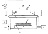
図1に、本発明の第1実施形態に係る誘導結合型プラズマ源を搭載した加工装置の断面図を示す。図1において、真空容器1内にガス供給装置2から所定のガスを導入しつつ、排気装置としてのターボ分子ポンプ3により排気を行い、真空容器1内を所定の圧力に保ちながら、コイル用高周波電源4により周波数13.56MHzの高周波電力を、プラズマ源としての誘電板5上のコイル6に供給することにより、真空容器1内にプラズマが発生する。電極7上には、被処理物としての基板8が載置される。アルミニウム(導体)製のマスク9は、基板8の近傍に配置され、マスク9には微小な貫通穴が設けられている。マスク用高周波電源10より、マスク9に500kHzの高周波電力を供給することができる。マスク9の端部に距離計測装置としてのレーザー変位計11が設けられており、基板8とマスク9との距離が計測できる。レーザー変位計11により得られた情報は、距離制御装置としてのモーター12にフィードバックされ、ギアボックス13を介してマスク9の位置を変化させることにより、基板8とマスク9の距離が所望の値に保たれる。また、シーケンサ14により、マスク9と基板8の距離を徐々に大きく、または徐々に小さくするよう、プログラム可能となっている。
【0024】
図2に、本発明の第1実施形態に係る被処理物の加工方法の概念図を示す。マスク9には微小な貫通穴15が多数設けられており、マスク9に印加される高周波電力の影響により、マスク9の表面にはイオンシースが形成される。イオンシースにおいて、プラズマ中の活性粒子であるイオン16はマスク9の方向に加速されるが、貫通穴14を通じて漏れ出たイオン16が、基板8に高い運動エネルギーをもって衝突する。この作用により、基板8或いは基板8上に形成された薄膜などがエッチング加工され、マスク形状が転写される。
【0025】
このとき、マスク9と基板8との距離を徐々に大きくしていくと、貫通穴15から基板8へ向かうイオン束の広がりにより、基板8上の被エッチング領域が大きくなってくる。その結果、図3に示すような順テーパー形状を得ることが可能となる。なお、真空容器1内に発生させたプラズマを停止することなく、モーター12の動作を行えるよう、レーザー変位計11からのフィードバック用信号線等にはシールド対策が施されている。
【0026】
マスク9と基板8との距離を徐々に小さくした場合も、同様の順テーパー形状を得ることができる。
【0027】
以下に、具体的な加工条件の一例を示す。4フッ化炭素ガスを100sccm供給し、真空容器1内の圧力を1Paに保ちながら、コイル6に1000Wの高周波電力を供給し、真空容器1内にプラズマを発生させる。マスク9に200Wの高周波電力を供給しつつ、マスク9と基板8の距離を100μm/分の速度で50μmから350μmまで3分間で変化させながら、基板8上に形成された多結晶シリコン膜のエッチングを行った。このとき、多結晶シリコン膜が600nmエッチングされ、断面形状は順テーパー形状であった。また、パターン底の寸法とパターン表面の寸法の差は1.2μmであり、テーパー角は45度であった。
【0028】
以上述べた本発明の第1実施形態において、真空容器内にプラズマを発生させるために、誘導結合型プラズマ源を用いた場合を例示したが、アンテナ式プラズマ源、マイクロ波プラズマ源、平行平板型プラズマ源、電子サイクロトロン共鳴型プラズマ源など、様々なプラズマ源を用いることができる。
【0029】
また、マスクが導体であり、かつ、マスクに高周波電力を印加する場合を例示したが、マスクに負の直流電圧を印加してもよい。或いは、絶縁体のコーティングを施されたマスクに、高周波電力を印加してもよい。或いは、被処理物を載置するための電極に高周波電力を印加することによっても、同様の加工を行うことができる。
【0030】
(第2の実施形態)
次に、本発明の第2実施形態について、図3乃至図5を参照して説明する。
【0031】
図4に、本発明の第2実施形態に係るマイクロプラズマ源を搭載した加工装置の断面図を示す。図4において、電極18上に載置された被処理物としての基板8の近傍に、マイクロプラズマ源17が配置され、マイクロプラズマ源17に100MHzの高周波電力を印加することにより、マイクロプラズマが発生する。このマイクロプラズマから漏れ出る活性粒子を基板8に作用させ、基板8を加工することができる。マイクロプラズマ源17の端部に距離計測装置としてのレーザー変位計11が設けられており、基板8とマイクロプラズマ源17との距離が計測できる。レーザー変位計11により得られた情報は、距離制御装置としてのモーター12にフィードバックされ、ギアボックス13を介してマイクロプラズマ源17の位置を変化させることにより、基板8とマイクロプラズマ源17の距離が所望の値に保たれる。また、シーケンサ14には、マイクロプラズマ源17と基板8の距離を徐々に大きく、または徐々に小さくなるようにプログラムが組み込まれている。
【0032】
図5は、マイクロプラズマ源17を図4の破線Aで切った断面図である。2枚の石英ガラス板19及び20が接着され、その間にキャピラリ21が形成されている。反応ガスはキャピラリ21の内部に導入され、基板8に向かってマイクロプラズマとなって噴出される。高周波電極22と接地電極23が石英ガラス板19及び20の両側に設けられ、高周波電極22には高周波電源24より高周波電力が供給される。マイクロプラズマ源17は1Paから数気圧まで動作可能であるが、典型的には103Paから大気圧までの範囲の圧力で動作する。
【0033】
このとき、マイクロプラズマ源17と基板8との距離を徐々に大きくしていくと、マイクロプラズマ源17から基板8へ向かう活性粒子の流れの広がりにより、基板8上の被エッチング領域が大きくなってくる。その結果、図3に示すような順テーパー形状を得ることが可能となる。なお、発生させたマイクロプラズマを停止することなく、モーター12の動作を行えるよう、レーザー変位計11からのフィードバック用信号線等にはシールド対策が施されている。
【0034】
マイクロプラズマ源17と基板8との距離を徐々に小さくした場合も、同様の順テーパー形状を得ることができる。
【0035】
以下に、具体的な加工条件の一例を示す。6フッ化硫黄ガスを5%含むヘリウムガスを2slm供給し、大気圧下でマイクロプラズマ源17に10Wの高周波電力を供給し、真空容器1内にプラズマを発生させる。マイクロプラズマ源17と基板8の距離を200μm/分の速度で500μmから1000μmまで2.5分間で変化させながら、シリコン基板8のエッチングを行った。このとき、シリコン基板が5μmエッチングされ、断面形状は順テーパー形状であった。また、パターン底の寸法とパターン表面の寸法の差は10μmであり、テーパー角は45度であった。
【0036】
以上述べた本発明の第2実施形態において、マイクロプラズマ源として平行平板型キャピラリタイプのものを用いる場合を例示したが、誘導結合型キャピラリタイプなど、他方式のキャピラリタイプや、マイクロギャップ方式、誘導結合型チューブタイプなど、様々なマイクロプラズマ源を用いることができる。
【0037】
また、被処理物を載置するための電極に高周波電力を印加することにより、マイクロプラズマ中のイオンを引き込む作用を強めることも可能である。
【0038】
以上述べた本発明の実施形態においては、本発明の適用範囲のうち、真空容器の形状、プラズマ源の構造及び配置等に関して様々なバリエーションのうちの一部を例示したに過ぎない。本発明の適用にあたり、ここで例示した以外にも様々なバリエーションが考えられることは、いうまでもない。
【0039】
また、多結晶シリコンやシリコン基板をエッチング加工する場合を例示したが、加工対象はこれらに限定されるものではなく、本発明は、種々の基板の加工、または、種々の膜がコーティングされた被処理物の加工に適用できる。
【0040】
また、エッチング加工に際して4フッ化炭素や6フッ化硫黄ガスを用いる場合を例示したが、ガスはこれに限定されるものではなく、被処理物の材質に応じて、マスクまたはマイクロプラズマ源を構成する物質とのエッチング選択比が高められるガスを選定することができる。
【0041】
また、距離計測装置としてレーザー変位計を用いる場合を例示したが、接触式センサや、原子間力を利用した非接触センサなどを利用することもできる。これらは、可能なコストと必要な精度に応じて選択することができる。
【0042】
また、マスクまたはマイクロプラズマ源と被処理物の距離を変化させながらエッチング加工する場合を例示したが、プラズマが停止している状態で距離を変化させる工程と、ある距離に保ちながらプラズマを発生させて加工する工程を繰り返してもよい。或いは、プラズマを継続して発生させながら、マスクまたは基板を載置する電極に印加する高周波電力または直流電力を停止した状態で距離を変化させる工程と、ある距離に保ちながらマスクまたは基板を載置する電極に高周波電力または直流電力を供給して加工する工程を繰り返してもよい。
【0043】
【発明の効果】
以上の説明から明らかなように、真空容器と、前記真空容器内にガスを供給するガス供給装置と、前記真空容器内を排気する排気装置と、前記真空容器内にプラズマを発生させるプラズマ源と、前記プラズマ源に高周波電力を供給する高周波電源と、前記真空容器内に配置された電極と、前記プラズマ源と前記電極との間かつ前記電極に対向して配置されると共に貫通穴が設けられたマスクと、前記真空容器内かつ前記電極に対向して設けられ前記電極表面に配置された前記被処理物と前記マスクとの距離をレーザーにより計測する距離計測装置と、前記距離計測装置にて得られた情報に基づき、前記マスクと前記被処理物との距離を変化させる距離制御装置とを備えたため、パターンニング形状を制御でき、かつ、加工精度に優れた加工を行うことができる。
【図面の簡単な説明】
【図1】本発明の第1実施形態に係る加工装置の構成を示す断面図
【図2】本発明の第1実施形態に係る被処理物の加工方法の概念図
【図3】本発明の実施形態における加工形状を示す図
【図4】本発明の第2実施形態に係る加工装置の構成を示す断面図
【図5】本発明の第2実施形態に係るマイクロプラズマ源の断面図
【図6】従来例で用いたパターンニング工程を示す図
【図7】従来例で用いた加工装置の構成を示す断面図
【図8】従来例で用いた加工装置の構成を示す断面図
【符号の説明】
1 真空容器
2 ガス供給装置
3 ターボ分子ポンプ
4 コイル用高周波電源
5 誘電板
6 コイル
7 電極
8 基板
9 マスク
10 マスク用高周波電源
11 レーザー変位計
12 モーター
13 ギアボックス
14 シーケンサ[0001]
BACKGROUND OF THE INVENTION
The present invention relates to a pressurized KoSo location, and non contact mask processing means to particularly unnecessary resist mask is characterized in processing means using a micro-plasma source.
[0002]
[Prior art]
In general, a resist process is used when patterning is performed on an object typified by a substrate having a thin film formed on the surface. An example is shown in FIG. In FIG. 6, first, a
[0003]
Since the resist process as described above is suitable for accurately forming a fine pattern, it has played an important role in the manufacture of electronic devices such as semiconductors. In addition, there is a drawback that the process is complicated.
[0004]
Therefore, a new processing method that does not use a resist process has been studied. As an example, FIG. 7 shows a conceptual diagram of non-contact mask etching. An object to be processed 8 is placed on the
[0005]
As another example, FIG. 8 shows a conceptual diagram of microplasma etching. A high-frequency power is supplied to a
[0006]
[Problems to be solved by the invention]
However, in the processing of the object to be processed described in the conventional example, there may be a problem that it is difficult to control the patterning shape formed on the surface of the object to be processed. As a result, there is a problem that processing accuracy is lowered.
[0007]
The present invention is the light of the conventional problems, it can be controlled patterned shape, and has an object to provide an excellent pressure KoSo location processing accuracy.
[0008]
[Means for Solving the Problems]
The processing apparatus of the present invention includes a vacuum vessel, a gas supply device for supplying gas into the vacuum vessel, an exhaust device for exhausting the vacuum vessel, a plasma source for generating plasma in the vacuum vessel, a high frequency power supply for supplying high frequency power to the plasma source, wherein the electrodes disposed in a vacuum container, is between and is arranged to face the electrode Rutotomoni penetrations holes between the electrode and the plasma source is provided a mask, a distance measuring device for measuring by a laser a distance between the object to be processed and the mask disposed on the electrode surface provided opposite to the vacuum vessel and the electrode, resulting in the distance measuring device And a distance control device that changes a distance between the mask and the object to be processed based on the obtained information.
[0009]
In the processing apparatus of the present gun onset bright, preferably, the distance control device is preferably operable without stopping the plasma generated in the vacuum chamber. It is also desirable to gradually increase the distance between the mask and the object to be processed. Alternatively, the distance between the mask and the object to be processed may be gradually reduced.
[0010]
Preferably, the mask is a conductor and a negative DC voltage is applied to the mask. Alternatively, the mask may be a conductor and high frequency power may be applied to the mask. Alternatively, the mask may be a conductor in which an insulator is coated, and high frequency power may be applied to the mask. Alternatively, it may be applied to high-frequency power to that electrodes be placed an object to be processed.
[0022]
DETAILED DESCRIPTION OF THE INVENTION
(First embodiment)
Hereinafter, a first embodiment of the present invention will be described with reference to FIGS. 1 to 3.
[0023]
FIG. 1 shows a cross-sectional view of a processing apparatus equipped with an inductively coupled plasma source according to the first embodiment of the present invention. In FIG. 1, while introducing a predetermined gas from a
[0024]
In FIG. 2, the conceptual diagram of the processing method of the to-be-processed object which concerns on 1st Embodiment of this invention is shown. The
[0025]
At this time, when the distance between the
[0026]
A similar forward tapered shape can be obtained even when the distance between the
[0027]
An example of specific processing conditions is shown below. While supplying 100 sccm of carbon tetrafluoride gas and keeping the pressure in the
[0028]
In the first embodiment of the present invention described above, the case where an inductively coupled plasma source is used to generate plasma in the vacuum vessel is illustrated, but an antenna type plasma source, a microwave plasma source, a parallel plate type Various plasma sources such as a plasma source and an electron cyclotron resonance plasma source can be used.
[0029]
Moreover, although the case where the mask is a conductor and high frequency power is applied to the mask has been illustrated, a negative DC voltage may be applied to the mask. Alternatively, high-frequency power may be applied to a mask coated with an insulator. Alternatively, the same processing can be performed by applying high-frequency power to an electrode on which the workpiece is placed.
[0030]
(Second Embodiment)
Next, a second embodiment of the present invention will be described with reference to FIGS.
[0031]
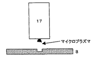
FIG. 4 shows a cross-sectional view of a processing apparatus equipped with a microplasma source according to the second embodiment of the present invention. In FIG. 4, a
[0032]
5 is a cross-sectional view of the
[0033]
At this time, when the distance between the
[0034]
A similar forward taper shape can be obtained even when the distance between the
[0035]
An example of specific processing conditions is shown below. Helium gas containing 5% sulfur hexafluoride gas is supplied at 2 slm, high frequency power of 10 W is supplied to the
[0036]
In the second embodiment of the present invention described above, the case where a parallel plate type capillary type is used as the microplasma source has been exemplified. However, other types of capillary types such as an inductively coupled capillary type, a microgap type, an induction type, etc. Various microplasma sources such as a coupled tube type can be used.
[0037]
In addition, by applying high-frequency power to the electrode for placing the object to be processed, it is possible to enhance the action of attracting ions in the microplasma.
[0038]
In the embodiment of the present invention described above, only a part of various variations in the scope of the present invention regarding the shape of the vacuum vessel, the structure and arrangement of the plasma source, and the like are merely illustrated. It goes without saying that various variations other than those exemplified here can be considered in applying the present invention.
[0039]
In addition, although the case where polycrystalline silicon or a silicon substrate is etched is illustrated, the object to be processed is not limited to these, and the present invention can be applied to processing various substrates or coatings coated with various films. Applicable to processing of processed products.
[0040]
Moreover, although the case where carbon tetrafluoride or sulfur hexafluoride gas is used in the etching process is exemplified, the gas is not limited to this, and a mask or a microplasma source is configured according to the material of the object to be processed. It is possible to select a gas that can increase the etching selectivity with the substance to be performed.
[0041]
Moreover, although the case where a laser displacement meter was used as a distance measuring device was illustrated, a contact sensor, a non-contact sensor using atomic force, or the like can also be used. These can be selected depending on the possible cost and the required accuracy.
[0042]
In addition, the case where the etching process is performed while changing the distance between the mask or the microplasma source and the object to be processed is exemplified, but the process of changing the distance while the plasma is stopped and the generation of the plasma while maintaining the certain distance. The processing step may be repeated. Alternatively, the step of changing the distance while the high frequency power or the DC power applied to the electrode on which the mask or substrate is placed is stopped while plasma is continuously generated, and the mask or substrate is placed while maintaining a certain distance. The process of supplying high frequency power or DC power to the electrode to be processed may be repeated.
[0043]
【The invention's effect】
As is apparent from the above description, a vacuum vessel, a gas supply device that supplies gas into the vacuum vessel, an exhaust device that exhausts the inside of the vacuum vessel, and a plasma source that generates plasma in the vacuum vessel; , a high frequency power supply for supplying high frequency power, an electrode disposed in said vacuum container, is between and Rutotomoni penetrations holes are arranged to face the electrode of the electrode and the plasma source is provided to the plasma source a mask which is the distance between the vacuum vessel and the processing object and the mask disposed on the electrode surface provided opposite to the electrode and the distance measuring device for measuring by a laser, the distance measuring device Based on the information obtained, a distance control device that changes the distance between the mask and the object to be processed is provided, so that the patterning shape can be controlled and processing with excellent processing accuracy can be performed. Ukoto can.
[Brief description of the drawings]
FIG. 1 is a cross-sectional view showing a configuration of a processing apparatus according to a first embodiment of the present invention. FIG. 2 is a conceptual diagram of a processing method for an object to be processed according to the first embodiment of the present invention. FIG. 4 is a cross-sectional view showing a configuration of a processing apparatus according to a second embodiment of the present invention. FIG. 5 is a cross-sectional view of a microplasma source according to the second embodiment of the present invention. 6 is a diagram showing the patterning process used in the conventional example. FIG. 7 is a cross-sectional view showing the configuration of the processing apparatus used in the conventional example. FIG. 8 is a cross-sectional view showing the configuration of the processing apparatus used in the conventional example. Explanation】
DESCRIPTION OF
Claims (7)
を特徴とする加工装置。A vacuum vessel, a gas supply device for supplying gas into the vacuum vessel, an exhaust device for exhausting the inside of the vacuum vessel, a plasma source for generating plasma in the vacuum vessel, and supplying high-frequency power to the plasma source to the high-frequency power source, an electrode disposed in said vacuum container, and during and mask opposed disposed Rutotomoni penetrations holes to the electrodes are provided between the electrode and the plasma source, the vacuum container and a distance measuring device for measuring a distance between the object to be processed and the mask disposed on the electrode surface provided opposite to the electrode by a laser, based on the information obtained by the distance measuring device, wherein A processing apparatus comprising: a distance control device that changes a distance between a mask and the workpiece.
Priority Applications (1)
| Application Number | Priority Date | Filing Date | Title |
|---|---|---|---|
| JP2002029231A JP3948295B2 (en) | 2002-02-06 | 2002-02-06 | Processing equipment |
Applications Claiming Priority (1)
| Application Number | Priority Date | Filing Date | Title |
|---|---|---|---|
| JP2002029231A JP3948295B2 (en) | 2002-02-06 | 2002-02-06 | Processing equipment |
Related Child Applications (1)
| Application Number | Title | Priority Date | Filing Date |
|---|---|---|---|
| JP2006216895A Division JP2006324691A (en) | 2006-08-09 | 2006-08-09 | Machining method and apparatus thereof |
Publications (2)
| Publication Number | Publication Date |
|---|---|
| JP2003234333A JP2003234333A (en) | 2003-08-22 |
| JP3948295B2 true JP3948295B2 (en) | 2007-07-25 |
Family
ID=27773606
Family Applications (1)
| Application Number | Title | Priority Date | Filing Date |
|---|---|---|---|
| JP2002029231A Expired - Fee Related JP3948295B2 (en) | 2002-02-06 | 2002-02-06 | Processing equipment |
Country Status (1)
| Country | Link |
|---|---|
| JP (1) | JP3948295B2 (en) |
Families Citing this family (4)
| Publication number | Priority date | Publication date | Assignee | Title |
|---|---|---|---|---|
| JP2005206939A (en) * | 2003-12-26 | 2005-08-04 | Seiko Epson Corp | Thin film formation method, thin film formation equipment, method of manufacturing organic electroluminescence device, organic electroluminescence device, and electronic apparatus |
| US7309842B1 (en) * | 2004-03-19 | 2007-12-18 | Verionix Incorporated | Shielded monolithic microplasma source for prevention of continuous thin film formation |
| JP4613321B2 (en) * | 2005-06-27 | 2011-01-19 | 国立大学法人京都大学 | Electromagnetic wave control element, electromagnetic wave control device, and electromagnetic wave control method |
| JP5696418B2 (en) * | 2010-09-29 | 2015-04-08 | 凸版印刷株式会社 | Photomask manufacturing method |
-
2002
- 2002-02-06 JP JP2002029231A patent/JP3948295B2/en not_active Expired - Fee Related
Also Published As
| Publication number | Publication date |
|---|---|
| JP2003234333A (en) | 2003-08-22 |
Similar Documents
| Publication | Publication Date | Title |
|---|---|---|
| KR101333924B1 (en) | Method and system for controlling the uniformity of a ballistic electron beam by rf modulation | |
| KR100498584B1 (en) | Plasma Treatment Equipment and Plasma Treatment Methods | |
| US5330606A (en) | Plasma source for etching | |
| US5345145A (en) | Method and apparatus for generating highly dense uniform plasma in a high frequency electric field | |
| JP3726477B2 (en) | Plasma processing apparatus and plasma processing method | |
| KR970005035B1 (en) | Method and apparatus for generating highly dense uniform plasma by use of a high frequency rotating electric field | |
| US20010037770A1 (en) | Plasma processing apparatus and processing method | |
| US20080068774A1 (en) | Plasma processing method and apparatus | |
| JP3706027B2 (en) | Plasma processing method | |
| US6909086B2 (en) | Neutral particle beam processing apparatus | |
| US20030010453A1 (en) | Plasma processing apparatus and plasma processing method | |
| JP3948295B2 (en) | Processing equipment | |
| JP2006324691A (en) | Machining method and apparatus thereof | |
| JP3223692B2 (en) | Dry etching method | |
| JP2001015495A (en) | Device and method for plasma treatment | |
| JP2851765B2 (en) | Plasma generation method and apparatus | |
| JP2006114933A (en) | Reactive ion etching device | |
| JP2005175503A (en) | Plasma processing device and plasma processing method | |
| WO2023275958A1 (en) | Method for regenerating inner wall member | |
| KR970010266B1 (en) | Plasma generating method and apparatus thereof | |
| JPH025413A (en) | Plasma processor | |
| US20010021550A1 (en) | Plasma processing method and apparatus | |
| JPH10330970A (en) | Reactive ion etching device | |
| JP2000012529A (en) | Surface machining apparatus | |
| JP2001110597A (en) | Magnetic neutral ray discharge plasma generating apparatus |
Legal Events
| Date | Code | Title | Description |
|---|---|---|---|
| A621 | Written request for application examination |
Free format text: JAPANESE INTERMEDIATE CODE: A621 Effective date: 20041216 |
|
| RD01 | Notification of change of attorney |
Free format text: JAPANESE INTERMEDIATE CODE: A7421 Effective date: 20050704 |
|
| A977 | Report on retrieval |
Free format text: JAPANESE INTERMEDIATE CODE: A971007 Effective date: 20060608 |
|
| A131 | Notification of reasons for refusal |
Free format text: JAPANESE INTERMEDIATE CODE: A131 Effective date: 20060613 |
|
| A521 | Written amendment |
Free format text: JAPANESE INTERMEDIATE CODE: A523 Effective date: 20060810 |
|
| A131 | Notification of reasons for refusal |
Free format text: JAPANESE INTERMEDIATE CODE: A131 Effective date: 20070206 |
|
| A521 | Written amendment |
Free format text: JAPANESE INTERMEDIATE CODE: A523 Effective date: 20070302 |
|
| TRDD | Decision of grant or rejection written | ||
| A01 | Written decision to grant a patent or to grant a registration (utility model) |
Free format text: JAPANESE INTERMEDIATE CODE: A01 Effective date: 20070327 |
|
| A61 | First payment of annual fees (during grant procedure) |
Free format text: JAPANESE INTERMEDIATE CODE: A61 Effective date: 20070409 |
|
| FPAY | Renewal fee payment (event date is renewal date of database) |
Free format text: PAYMENT UNTIL: 20110427 Year of fee payment: 4 |
|
| FPAY | Renewal fee payment (event date is renewal date of database) |
Free format text: PAYMENT UNTIL: 20120427 Year of fee payment: 5 |
|
| FPAY | Renewal fee payment (event date is renewal date of database) |
Free format text: PAYMENT UNTIL: 20130427 Year of fee payment: 6 |
|
| FPAY | Renewal fee payment (event date is renewal date of database) |
Free format text: PAYMENT UNTIL: 20130427 Year of fee payment: 6 |
|
| FPAY | Renewal fee payment (event date is renewal date of database) |
Free format text: PAYMENT UNTIL: 20140427 Year of fee payment: 7 |
|
| LAPS | Cancellation because of no payment of annual fees |